JP3892115B2 - Display and device with display - Google Patents
Display and device with display Download PDFInfo
- Publication number
- JP3892115B2 JP3892115B2 JP19650097A JP19650097A JP3892115B2 JP 3892115 B2 JP3892115 B2 JP 3892115B2 JP 19650097 A JP19650097 A JP 19650097A JP 19650097 A JP19650097 A JP 19650097A JP 3892115 B2 JP3892115 B2 JP 3892115B2
- Authority
- JP
- Japan
- Prior art keywords
- region
- film
- display
- pixel
- pixel electrode
- Prior art date
- Legal status (The legal status is an assumption and is not a legal conclusion. Google has not performed a legal analysis and makes no representation as to the accuracy of the status listed.)
- Expired - Fee Related
Links
Images


Description
【0001】
【産業上の利用分野】
本明細書で開示する発明は、アクティブマトリクス型の液晶ディスプレイの構造に関する。
【0002】
【従来の技術】
アクティブマトリクス型の液晶ディスプレイが知られている。これは、マトリクス状に配置された各画素に薄膜トランジスタ(TFTと称される)を配置した構造を有している。
【0003】
液晶ディスプレイには、反射型と透過型との2つの形式がある。一般に透過型の液晶ディスプレイにおいては、画素に周辺部の縁の領域における液晶の配向不良による表示のぼけを抑制するためにブラックマトリクス(BMと称される)という遮蔽膜を配置する構成が必要とされる。
【0004】
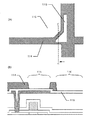
ブラックマトリクスには、画素に配置されるTFTを遮蔽する役割もある。図6に示すのは、従来の透過型アクティブマトリクスディスプレイの画素部分の断面、特にTFTが配置されている部分の断面である。
【0005】
図6において、200と202は樹脂膜である。樹脂膜を用いるのは、その表面を平坦にできるからである。
【0006】
201がブラックマトリクスの一部である。図6においては、ブラックマトリクス201はTFTを遮蔽する役割を有している。
【0007】
204はコンタクト用の開口であり、ここでITO電極203がTFTのドレイン電極206に開口204を介してコンタクトしている。
【0008】
ブラックマトリクスは遮光性を有する金属材料でもって構成されている。ブラックマトリクスは、画素電極203と接触してはいけないので、205で示す部分では、多少のマージンをもってパターンが形成されている。
【0009】
この構成においては、ブラックマトリクス201と画素電極203との接触が問題となる。といって合わせマージンを大きくとると、ブラックマトリクスの遮光膜として機能が損なわれてしまう。
【0010】
【発明が解決しようとする課題】
本明細書で開示する発明は、上述するブラックマトリクスと画素電極とが接触してしまう問題を解決することを課題とする。
【0011】
【課題を解決するための手段】
本明細書で開示する発明の一つは、
薄膜トランジスタと、
該薄膜トランジスタに接続された画素電極と、
前記薄膜トランジスタと前記画素電極との間に形成された遮光性を有する樹脂材料でなる膜と、
を有し、
前記樹脂材料でなる膜には、
前記画素電極と前記薄膜トランジスタとを接続するための開口と、
画素に対応する領域に形成された開口と、
が形成されていることを特徴とするディスプレイである。
【0012】
上記構成の具体的な例を図5に示す。図5には、薄膜トランジスタの不純物領域にドレイン電極110(容量を構成する一方の導電膜パターン)が接続され、さらにこの電極110に画素電極120が開口119において接続されている。
【0013】
114が遮光性を有する樹脂膜であり、この樹脂膜に形成された開口119において、薄膜トランジスタの不純物領域にコンタクトした電極110に画素電極120がコンタクトしている。結果として、画素電極120は薄膜トランジスタの不純物領域に接続(電気的に接続)された状態となっている。
【0014】
また、樹脂膜114には、薄膜トランジスタと画素電極120とを接続するための開口119の他に画素に対応する領域に形成した開口116(図3参照)が形成されている。
【0015】
こうした構成を採用することで、図5(B)の122で示される部分において、画素電極120とブラックマトリクスとして機能する樹脂膜114との形成マージンやショートの問題に関する懸念を排除した透過型の液晶ディスプレイを得ることができる。
【0016】
本明細書において画素というのは、表示に際してパネルを透過する光の光学変調に寄与する領域のことをいう。画面面積に対する画素の総面積の割合が開口率となる。画素とならない領域の例としては、配線、薄膜トランジスタの閉める領域、ブラックマトリクスによって遮蔽される領域を挙げることができる。
【0017】
上記構成においては、図3に示されるように樹脂膜114に開口115を形成し、この部分に補助容量を形成する。また開口115は、TFTの上方(活性層の上方)に形成される。こうすることで、大容量の補助容量を形成することができ、しかも画素の開口率を低下させない構成とすることができる。
【0018】
開口115は、薄膜トランジスタの活性層の少なくとも一部の領域に重なった領域に形成することが好ましい。そして、補助容量の他方の電極を構成する容量線117(図4参照)を薄膜トランジスタの活性層の大部分に重なるようにして形成することが好ましい。
【0019】
ここでいう大部分というのは、面積比率で50%以上、好ましくは75%以上であることをいう。この面積比率が大きい方が開口率を高める上では好ましい。
【0020】
このような構成とすることで、補助容量を形成した場合に問題となる開口率の低下を抑制することができる。
【0021】
また、この構成では、薄膜トランジスタの不純物領域(ドレイン領域)104(図1参照)に接続されたドレイン電極110と容量線117との間の誘電体膜113を薄く、また誘電率の高い材料とすることができるので、高い容量を確保することができる。
【0022】
以上の構成は、そのような構成を有するディスプレイを備えた装置としても有用なものとなる。即ち、高開口率であるが故に高い画質を備えたディスプレイを備えた携帯情報端末等の装置として構成も発明に含まれる。
【0023】
【発明の実施の形態】
図5の114で示されるように層間絶縁膜の一部を遮光性の樹脂材料でもって構成する。この樹脂層114は図4に示されるように画素領域を取り囲むようにパターニングされ、ブラックマトリクスとして機能する。
【0024】
この構成では、ブラックマトリクス114に直接開口を形成し、そこで画素電極120のコンタクトが形成される。こうすることで従来において必要とされていた画素電極のコンタクト用の開口部におけるブラックマトリクスとの位置合わせマージンを省くことができる。
【0025】
また、従来技術において問題となっていた画素電極とブラックマトリクスとの接触によるショートの問題を懸念する必要がないものとすることができる。
【0026】
図5に示す構成では、図3に示すようにブラックマトリクスとなるパターン114の画素電極が設けられる領域116と補助容量が設けられる領域115とでパターンが設けられていない構造となっている。
【0027】
特に115で示される領域には、ブラックマトリクスを構成する樹脂材料が設けられておらず、この部分で補助容量が形成される構造となっている。この補助容量は、画素TFTの上部に形成される。
【0028】
こういう構成を採用することで、透過型の液晶表示装置において、大きな容量を形成でき、しかも画素の開口率の低下を抑制したものとすることができる。
【0029】
【実施例】
〔実施例1〕
本実施例では、透過型のアクティブマトリクス型液晶パネルを構成するTFT基板側の作製工程を示す。
【0030】
TFT基板側というのは、アクティブマトリクス回路や周辺駆動回路が設けられた基板側のことである。
【0031】
図1〜図5に本実施例の作製工程を示す。なお、各図において、上側の図の点線で切った断面が下側に示されている。
【0032】
まず図1(B)に示すようにガラス基板100上に結晶性珪素膜でなる活性層101を形成する。ここでは活性層101の膜厚を50nmとする。
【0033】
なお、図1において図1(A)のA−A’で切った断面が図1(B)である。
【0034】
ガラス基板は、その表面に酸化珪素膜や酸化窒化珪素膜等の下地膜が成膜されているものを用いてもよい。また、基板としては、石英基板や絶縁膜が成膜された半導体基板を用いてもよい。(これら本明細書に開示する発明に利用できる基板を総称して絶縁表面を有する基板と称する)
【0035】
結晶性珪素膜の作製方法としては以下のような例を挙げることができる。まず、非晶質珪素膜を減圧熱CVD法で成膜する。次にレーザー光の照射を行うことにより、この非晶質珪素膜を結晶化させ、結晶性珪素膜とする。
【0036】
結晶性珪素膜を得たら、それをパターニングして活性層のパターン101を形成する。
【0037】
活性層パターン101を形成したら、ゲイト絶縁膜として機能する酸化珪素膜102をプラズマCVD法により、100nmの厚さに成膜する。
【0038】
さらにタングステンシリサイド材料を用いてゲイト電極103(ゲイト配線)を形成する。
【0039】
ゲイト電極を構成する材料としては、各種シリサイド材料、アルミニウム、タンタル、さらにはそれらの膜の積層膜等を用いることができる。
【0040】
ゲイト電極105を形成したら、ゲイト電極のパターンをマスクとして不純物イオンの注入を行う。
【0041】
この工程は、以下の2種類の方法を用いることができる。
【0042】
(1)イオン注入法と称される方法。これは、質量分離を行って、ドーパントの選別を行い、選別されたドーパント元素を加速注入する方法である。
【0043】
(2)プラズマドーピング法と呼ばれる方法。これは、質量分離を行わなず、プラズマ中から引き出されたイオン化したドーパント元素を加速注入する方法。
【0044】
このドーピング工程において、図1(A)の活性層パターン101の露呈した領域にドーピングが行われる。
【0045】
ここでは、Nチャネル型のTFTを作製するためにN型を付与する不純物のドーピングを行う。ここではN型を付与する不純物として燐(P)を用いる。
【0046】
もしPチャネル型のTFTを作製するのであれば、P型を付与する不純物のドーピングを行う。P型を付与する不純物としては、ボロン(B)を挙げることができる。
【0047】
ドーピングが終了したらレーザー光の照射を行い、ドーパントの活性化と被ドーピング領域の結晶性の回復とを行う。
【0048】
こうして図1(B)に示す状態を得る。この状態では、104と106の領域が不純物領域となる。特に104の領域がTFTのドレイン領域となる。また、105の領域はチャネル領域となる。
【0049】
図1(B)の状態を上面から見たものを図1(A)に示す。
【0050】
本実施例に示すTFTは、ゲイト配線103が活性層101を3ヶ所で横切っている。このゲイト配線103が横切った部分の活性層の領域がチャネル領域となる。チャネル領域の一つは、図1(B)の105で示される領域である。
【0051】
この構造では、活性層中にチャネル領域が3ヶ所設けられる。このような構造は、等価的に3つのTFTが直列に接続されたものと見ることができる。
【0052】
次に図2(B)に示すように層間絶縁膜として窒化珪素膜107を200nmの厚さにプラズマCVD法でもって成膜する。
【0053】
そして、アクリル樹脂膜108をスピンコート法でもって成膜する。アクリル樹脂膜は表面が平坦化されるように成膜する。またその膜厚は、最小の部分で700nmとなるようにする。(図2(B))
【0054】
次にコンタクトホール109を形成する。そして図示しない金属膜を成膜し、それをパターニングすることにより、110で示すパターンと111で示すパターンとを形成する。
【0055】
パターン110と111とを構成する金属膜は、80nm厚のチタン膜と400nm厚のアルミニウム膜と80nm厚のチタン膜とを積層したものを用いる。なお、各膜はスパッタ法で成膜する。
【0056】
ここで、110のパターンは、TFTのドレイン領域にコンタクト用の開口109でコンタクトしたドレイン電極である。このパターン110は、後に補助容量の一方の電極として機能する。また、TFTを遮光する遮光膜としても機能する。
【0057】
111のパターンは、ソース線であり、TFTのソース領域にコンタクト用の開口112でコンタクトしている。このソース線111に画素に供給する信号電圧が供給される。
【0058】
ソース線111は、ゲイト線103と組となってアクティブマトリクス領域に格子状に配置される。
【0059】
図2において、図2(A)のB−B’で切った断面が図2(B)に示されている。
【0060】
図2に示す状態を得たら、図3(B)に示すように窒化珪素膜113を50nmの厚さにプラズマCVD法でもって成膜する。
【0061】
さらに黒い顔料を含有させた図示しないアクリル樹脂膜を成膜する。そして、この樹脂膜をパターニングすることにより、図3の114で示すパターンを形成する。
【0062】
樹脂膜パターン114は、ブラックマトリクスとして機能する樹脂膜である。この樹脂膜パターン114には、画素電極が形成される部分116と補助容量が形成される部分115に開口が形成され、その部分で窒化珪素膜113が露呈している。(その部分のパターンが抜かれている)
【0063】
ブラックマトリクスとして機能する樹脂膜114は、後に形成される画素電極の周縁の縁に一部重なるように形成される。
【0064】
次に図示しないチタン膜を400nmの厚さに成膜する。そしてその膜をパターニングすることにより、117で示すパターンを形成する。(図4)
【0065】
この117で示すパターンは、容量線であり、ソース線111に平行に(形成される層が異なるが)形成される。そして各画素において、画素TFTのドレイン電極110を一方の電極とし、この容量線を他方の電極として、補助容量が形成される。この窒化珪素膜113がこの補助容量の誘電体膜となる。
【0066】
図4の樹脂膜114に形成される開口部115において、ドレイン電極110と容量線パターン117とは、窒化珪素膜113を介して補助容量を形成している。
【0067】
この補助容量は、TFTが設けられた領域上にほぼ重なって形成されるので、画素の開口率の低下を防ぐことができる。また、この補助容量によって画素TFTが遮光される構造となる。
【0068】
なお、図4(A)のD−D’で切った断面が図4(B)で示される。
【0069】
次に図5に示されるように第2のアクリル樹脂膜118を成膜する。そして、開口119を形成し、さらに図示しないITO膜を成膜する。そしてこのITO膜をパターニングして、120及び121で示されるパターンを形成する。
【0070】
120及び121のITOパターンは、図5(A)に示されるように上下に隣合う画素電極のパターンである。ITO以外には、一般に透明導電膜と称される透過性の導電膜を用いることができる。
【0071】
なお、図5において、(A)のE−E’で切った断面が図5(B)である。
【0072】
本実施例では、図5(B)の122で示す部分において、画素電極120のコンタクト開口119がブラックマトリクスを構成する樹脂膜114に直接形成される構造となっている。
【0073】
こうすることで、コンタクト部におけるブラックマトリクス114と画素電極120とを合わせマージン等を考慮する必要がないものとすることができる。
【0074】
また、画素電極とブラックマトリクスとがショートしてしまうような問題もない。
【0075】
本実施例では、透過型の液晶パネルでブラックマトリクスとして絶縁性の樹脂材料を用い、画素電極のコンタクト部の開口をこの樹脂材料に直接形成しているので、画素電極とTFTとのコンタクト部における位置合わせマージンの問題や画素電極とブラックマトリクスとのショートの問題を回避することができる。
【0076】
また、ブラックマトリクスを構成する樹脂膜に、
(1)画素電極のTFTへのコンタクト用の開口
(2)画素電極部分に対応する領域の開口
(3)補助容量を形成するための開口
を形成することにより、透過型の液晶パネルとすることができる。
【0077】
また、TFTの上方に重なるようにして補助容量を形成することで、画素の開口率を最大限高めることができる。即ち、補助容量を設けることで発生する画素の開口率の低下を抑制することができる。
【0078】
〔実施例2〕
本実施例は、実施例1に示す構成において、TFTの構造をボトムゲイト型とした場合の例を示す。
【0079】
図7に本実施例の構造を示す。図7において、(A)のE−E’で切った断面を(B)に示す。
【0080】
図7において、図1と同じ符号が付与されている部分は、実施例1に示すものと同じである。
【0081】
図7に示す構成で特徴とするのは、TFTをボトムゲイト型のものとした点である。
【0082】
ボトムゲイト型のTFTは、ゲイト電極703を覆ってゲイト絶縁膜702が設けられ、さらに一導電型とされた不純物領域702と704、さらにチャネル領域となる705が形成された活性層が設けられた構造を有している。
【0083】
活性層のパターンは、実施例1に示したものと同様なものとなっている。即ち、図1の101で示すものであるような形状を有し、ゲイト線が3ヶ所で交差し、その部分でチャネル領域が形成されているような構造を有している。
【0084】
本実施例においては、不純物領域を不純物イオンのドーピングによって形成したものとなっている。
【0085】
〔実施例3〕
本実施例では、発明を利用した装置の例を示す。図8(A)に示すのは、携帯型の情報処理端末である。この情報処理端末は、本体2001にアクティブマトリクス型の液晶ディスプレイまたはアクティブマトリクス型のELディスプレイ、集積化回路、さらに外部から情報を取り込むためのカメラ部2002を備えている。
【0086】
カメラ部2002には、受像部2003と操作スイッチ2004が配置されている。
【0087】
情報処理端末は、今後益々その携帯性を向上させるために薄く、また軽くなるもと考えられている。
【0088】
このような構成においては、アクティブマトリクス型のディスプレイ2005が形成された基板上周辺駆動回路や演算回路や記憶回路がTFTでもって集積化されることが好ましい。
【0089】
さらに高微細な表示を明るい画面でしかも低消費電力で実現するため、より高い開口率を有したアクティブマトリクス型表示装置が必要とされる。
【0090】
このような要求を満たす液晶表示装置として、他の実施例で示すような構成を採用することは有用である。
【0091】
図8(B)に示すのは、ヘッドマウントディスプレイである。この装置は、アクティブマトリクス型の液晶ディスプレイやELディスプレイ2102を本体2101に備えている。また、本体2101は、バンド2103で頭に装着できるようになっている。
【0092】
図8(C)に示すのは、カーナビゲーション装置である。この装置は、本体2201に液晶表示装置2202と操作スイッチ2203を備え、アンテナ2204で受診した信号によって、地理情報等を表示する機能を有している。
【0093】
図8(D)に示すのは、携帯電話である。この装置は、本体2301にアクティブマトリクス型の液晶表示装置2304、操作スイッチ2305、音声入力部2303、音声出力部2302、アンテナ2306を備えている。
【0094】
また、最近は、(A)に示す携帯型情報処理端末と(D)に示す携帯電話とを組み合わせたような構成も商品化されている。
【0095】
図8(E)に示すのは、携帯型のビデオカメラである。これは、本体2401に受像部2406、音声入力部2403、操作スイッチ2404、アクティブマトリクス型の液晶ディスプレイ2402、バッテリー2405を備えている。
【0096】
ここでは、液晶表示装置としては、透過型のものを用いることとなる。
【0097】
〔発明に関するその他の構成に関して〕
本明細書で開示する発明においては、TFTの形式として特に限定されるものではない。また、活性層を構成する半導体の種類やその結晶性に関しても特に限定されるものではない。
【0098】
また、LDD技術やオフセット技術、さらにはチャネルドーピング技術等の改良技術を備えたTFTであってもよい。これは、必要に応じて適時選択することができる。
【0099】
また本明細書で開示する発明は、透過型のアクティブマトリクス型液晶ディスプレイであれば利用することができ、周辺駆動回路が外付け型であるか内蔵型であるかは問われない。
【0100】
【発明の効果】
本明細書で開示する発明を採用することにより、金属材料でなるBMと画素電極とが接触してしまう問題を解決することができる。また作製工程を簡略化することができる。
【0101】
そして高い開口率を有し、しかも高い生産歩留りを有する透過型の液晶ディスプレイを得ることができる。
【図面の簡単な説明】
【図1】 発明を利用したアクティブマトリクス型液晶ディスプレイの画素領域の作製工程を示す図。
【図2】 発明を利用したアクティブマトリクス型液晶ディスプレイの画素領域の作製工程を示す図。
【図3】 発明を利用したアクティブマトリクス型液晶ディスプレイの画素領域の作製工程を示す図。
【図4】 発明を利用したアクティブマトリクス型液晶ディスプレイの画素領域の作製工程を示す図。
【図5】 発明を利用したアクティブマトリクス型液晶ディスプレイの画素領域の作製工程を示す図。
【図6】 従来の技術におけるアクティブマトリクス型液晶ディスプレイの画素領域を示す図。
【図7】 発明を利用したアクティブマトリクス型液晶ディスプレイの画素領域の作製工程を示す図。
【図8】 発明を利用した装置の例を示す図。
【符号の説明】
100 ガラス基板
101 活性層パターン
102 ゲイト絶縁膜
103 ゲイト電極(ゲイト配線)(活性層との交差部がゲイト電極)
104 不純物領域(導電型を付与された領域)
105 チャネル領域
106 不純物領域(導電型を付与された領域)
107 窒化珪素膜(層間絶縁膜)
108 アクリル樹脂膜(層間絶縁膜)
109 コンタクト用の開口
110 ドレイン電極(補助容量の一方の電極)
111 ソース線
112 TFTのソース領域とソース線とのコンタクト
113 窒化珪素膜(補助容量の誘電体膜)
114 顔料含有のアクリル樹脂膜でなるブラックマトリクス
115 補助容量用の開口(アクリル樹脂膜に形成された開口)
116 画素領域に形成された開口
117 容量線(補助容量の他方の電極)
118 アクリル樹脂膜(層間絶縁膜)
119 画素電極のコンタクト用の開口
120 画素電極
121 画素電極
122 コンタクト開口部[0001]
[Industrial application fields]
The invention disclosed in this specification relates to a structure of an active matrix liquid crystal display.
[0002]
[Prior art]
An active matrix type liquid crystal display is known. This has a structure in which a thin film transistor (referred to as TFT) is arranged in each pixel arranged in a matrix.
[0003]
There are two types of liquid crystal displays, a reflective type and a transmissive type. In general, a transmissive liquid crystal display requires a configuration in which a shielding film called a black matrix (referred to as BM) is arranged in a pixel in order to suppress display blur due to liquid crystal alignment failure in a peripheral edge region. Is done.
[0004]
The black matrix also serves to shield the TFTs arranged in the pixels. FIG. 6 shows a cross section of a pixel portion of a conventional transmissive active matrix display, particularly a cross section of a portion where a TFT is disposed.
[0005]
In FIG. 6,
[0006]
201 is a part of the black matrix. In FIG. 6, the
[0007]
[0008]
The black matrix is made of a light-shielding metal material. Since the black matrix must not be in contact with the
[0009]
In this configuration, the contact between the
[0010]
[Problems to be solved by the invention]
An object of the invention disclosed in this specification is to solve the above-described problem of contact between the black matrix and the pixel electrode.
[0011]
[Means for Solving the Problems]
One of the inventions disclosed in this specification is:
A thin film transistor;
A pixel electrode connected to the thin film transistor;
A film formed of a light-shielding resin material formed between the thin film transistor and the pixel electrode;
Have
In the film made of the resin material,
An opening for connecting the pixel electrode and the thin film transistor;
An opening formed in a region corresponding to the pixel;
The display is characterized in that is formed.
[0012]
A specific example of the above configuration is shown in FIG. In FIG. 5, a drain electrode 110 (one conductive film pattern forming a capacitor) is connected to an impurity region of the thin film transistor, and a
[0013]
[0014]
Further, in the
[0015]
By adopting such a structure, a transmissive liquid crystal that eliminates concerns about the formation margin and short-circuit problem between the
[0016]
In this specification, a pixel refers to a region that contributes to optical modulation of light transmitted through a panel during display. The ratio of the total area of the pixels to the screen area is the aperture ratio. Examples of the region that does not become a pixel include a wiring, a region where a thin film transistor is closed, and a region shielded by a black matrix.
[0017]
In the above configuration, as shown in FIG. 3, an
[0018]
The opening 115 is preferably formed in a region overlapping with at least a partial region of the active layer of the thin film transistor. The capacitor line 117 (see FIG. 4) constituting the other electrode of the auxiliary capacitor is preferably formed so as to overlap most of the active layer of the thin film transistor.
[0019]
Here, the majority means that the area ratio is 50% or more, preferably 75% or more. A larger area ratio is preferable for increasing the aperture ratio.
[0020]
By adopting such a configuration, it is possible to suppress a decrease in aperture ratio that becomes a problem when an auxiliary capacitor is formed.
[0021]
Further, in this configuration, the
[0022]
The above configuration is also useful as a device including a display having such a configuration. That is, the invention includes a configuration as a device such as a portable information terminal provided with a display having a high image quality because of its high aperture ratio.
[0023]
DETAILED DESCRIPTION OF THE INVENTION
As shown by 114 in FIG. 5, a part of the interlayer insulating film is made of a light-shielding resin material. As shown in FIG. 4, the
[0024]
In this configuration, an opening is formed directly in the
[0025]
Further, it is possible to eliminate the need for concern about a short circuit due to contact between the pixel electrode and the black matrix, which has been a problem in the prior art.
[0026]
In the configuration shown in FIG. 5, as shown in FIG. 3, a pattern is not provided between the
[0027]
In particular, the region indicated by 115 is not provided with a resin material constituting the black matrix, and has a structure in which an auxiliary capacitance is formed in this portion. The auxiliary capacitor is formed on the pixel TFT.
[0028]
By adopting such a configuration, a large capacity can be formed in the transmissive liquid crystal display device, and a decrease in the aperture ratio of the pixel can be suppressed.
[0029]
【Example】
[Example 1]
In this embodiment, a manufacturing process on the side of a TFT substrate constituting a transmissive active matrix liquid crystal panel is shown.
[0030]
The TFT substrate side is the substrate side on which an active matrix circuit and a peripheral drive circuit are provided.
[0031]
1 to 5 show a manufacturing process of this embodiment. In each figure, a cross section cut by a dotted line in the upper figure is shown on the lower side.
[0032]
First, an
[0033]
Note that FIG. 1B shows a cross section taken along line AA ′ of FIG. 1A in FIG.
[0034]
As the glass substrate, a glass substrate on which a base film such as a silicon oxide film or a silicon oxynitride film is formed may be used. As the substrate, a quartz substrate or a semiconductor substrate on which an insulating film is formed may be used. (These substrates that can be used in the invention disclosed in this specification are collectively referred to as substrates having an insulating surface.)
[0035]
Examples of the method for manufacturing the crystalline silicon film include the following. First, an amorphous silicon film is formed by a low pressure thermal CVD method. Next, the amorphous silicon film is crystallized by irradiating with laser light to obtain a crystalline silicon film.
[0036]
Once the crystalline silicon film is obtained, it is patterned to form an
[0037]
After the formation of the
[0038]
Further, a gate electrode 103 (gate wiring) is formed using a tungsten silicide material.
[0039]
As a material constituting the gate electrode, various silicide materials, aluminum, tantalum, and a laminated film of these films can be used.
[0040]
After the
[0041]
In this step, the following two methods can be used.
[0042]
(1) A method called an ion implantation method. This is a method of performing mass separation, selecting dopants, and accelerating the selected dopant elements.
[0043]
(2) A method called a plasma doping method. This is a method of accelerating and implanting an ionized dopant element extracted from plasma without mass separation.
[0044]
In this doping step, doping is performed on the exposed region of the
[0045]
Here, in order to manufacture an N-channel TFT, doping of an impurity imparting N-type is performed. Here, phosphorus (P) is used as an impurity imparting N-type.
[0046]
If a P-channel TFT is manufactured, doping with an impurity imparting P-type is performed. As an impurity imparting P-type, boron (B) can be given.
[0047]
When the doping is completed, laser light irradiation is performed to activate the dopant and restore the crystallinity of the doped region.
[0048]
In this way, the state shown in FIG. In this state, the
[0049]
FIG. 1A shows the state of FIG. 1B viewed from above.
[0050]
In the TFT shown in this embodiment, the
[0051]
In this structure, three channel regions are provided in the active layer. Such a structure can be regarded as an equivalent of three TFTs connected in series.
[0052]
Next, as shown in FIG. 2B, a
[0053]
Then, an
[0054]
Next, a
[0055]
The metal film that forms the
[0056]
Here, a
[0057]
A
[0058]
The source lines 111 are paired with the
[0059]
2, a cross section taken along line BB ′ in FIG. 2A is shown in FIG.
[0060]
When the state shown in FIG. 2 is obtained, a
[0061]
Further, an acrylic resin film (not shown) containing a black pigment is formed. Then, by patterning this resin film, a pattern indicated by 114 in FIG. 3 is formed.
[0062]
The
[0063]
The
[0064]
Next, a titanium film (not shown) is formed to a thickness of 400 nm. Then, by patterning the film, a pattern indicated by 117 is formed. (Fig. 4)
[0065]
The pattern indicated by 117 is a capacitor line, and is formed in parallel to the source line 111 (although different layers are formed). In each pixel, a storage capacitor is formed using the
[0066]
In the
[0067]
Since this auxiliary capacitance is formed so as to substantially overlap the region where the TFT is provided, it is possible to prevent a decrease in the aperture ratio of the pixel. Further, the pixel TFT is shielded from light by the auxiliary capacitor.
[0068]
In addition, the cross section cut | disconnected by DD 'of FIG. 4 (A) is shown by FIG. 4 (B).
[0069]
Next, a second
[0070]
As shown in FIG. 5A, the
[0071]
In FIG. 5, a cross section taken along line EE ′ in FIG.
[0072]
In this embodiment, the
[0073]
By doing so, the
[0074]
Further, there is no problem that the pixel electrode and the black matrix are short-circuited.
[0075]
In this embodiment, an insulating resin material is used as a black matrix in the transmissive liquid crystal panel, and the opening of the contact portion of the pixel electrode is formed directly in this resin material. Therefore, in the contact portion between the pixel electrode and the TFT, It is possible to avoid the problem of alignment margin and the problem of short circuit between the pixel electrode and the black matrix.
[0076]
In addition, the resin film constituting the black matrix
(1) Opening for contact with TFT of pixel electrode (2) Opening of region corresponding to pixel electrode part (3) By forming an opening for forming auxiliary capacitance, a transmissive liquid crystal panel is obtained. Can do.
[0077]
Further, by forming the auxiliary capacitor so as to overlap the TFT, the aperture ratio of the pixel can be maximized. That is, it is possible to suppress a decrease in the aperture ratio of the pixel that occurs by providing the auxiliary capacitor.
[0078]
[Example 2]
This embodiment shows an example in which the TFT structure is a bottom gate type in the configuration shown in Embodiment 1.
[0079]
FIG. 7 shows the structure of this embodiment. In FIG. 7, the cross section cut by EE ′ in (A) is shown in (B).
[0080]
In FIG. 7, the same reference numerals as those in FIG. 1 are the same as those shown in the first embodiment.
[0081]
A feature of the configuration shown in FIG. 7 is that the TFT is of a bottom gate type.
[0082]
The bottom gate type TFT is provided with a
[0083]
The pattern of the active layer is the same as that shown in Example 1. That is, it has a shape as shown by 101 in FIG. 1, and has a structure in which gate lines intersect at three locations and a channel region is formed at that portion.
[0084]
In this embodiment, the impurity region is formed by doping impurity ions.
[0085]
Example 3
In this embodiment, an example of an apparatus using the invention is shown. FIG. 8A illustrates a portable information processing terminal. This information processing terminal includes a main body 2001 including an active matrix liquid crystal display or an active matrix EL display, an integrated circuit, and a camera unit 2002 for capturing information from the outside.
[0086]
In the camera unit 2002, an
[0087]
Information processing terminals are considered to become thinner and lighter in order to improve their portability.
[0088]
In such a configuration, it is preferable that the on-substrate peripheral driving circuit, the arithmetic circuit, and the memory circuit on which the active matrix display 2005 is formed are integrated with TFTs.
[0089]
Furthermore, in order to realize a high-definition display with a bright screen and low power consumption, an active matrix display device having a higher aperture ratio is required.
[0090]
It is useful to adopt a configuration as shown in another embodiment as a liquid crystal display device satisfying such requirements.
[0091]
FIG. 8B shows a head mounted display. This apparatus includes an active matrix liquid crystal display or an
[0092]
FIG. 8C shows a car navigation device. This apparatus includes a liquid
[0093]
FIG. 8D illustrates a mobile phone. This device includes an active matrix liquid crystal display device 2304, an
[0094]
Recently, a configuration in which the portable information processing terminal shown in (A) and the mobile phone shown in (D) are combined has been commercialized.
[0095]
FIG. 8E illustrates a portable video camera. The main body 2401 includes an image receiving unit 2406, an
[0096]
Here, a transmissive liquid crystal display device is used.
[0097]
[Regarding other configurations relating to the invention]
In the invention disclosed in this specification, the type of TFT is not particularly limited. Also, the type of semiconductor constituting the active layer and its crystallinity are not particularly limited.
[0098]
Further, the TFT may be provided with an improved technique such as an LDD technique, an offset technique, or a channel doping technique. This can be selected in a timely manner as required.
[0099]
The invention disclosed in this specification can be used as long as it is a transmissive active matrix liquid crystal display, and it does not matter whether the peripheral drive circuit is an external type or a built-in type.
[0100]
【The invention's effect】
By employing the invention disclosed in this specification, it is possible to solve the problem of contact between the BM made of a metal material and the pixel electrode. In addition, the manufacturing process can be simplified.
[0101]
A transmissive liquid crystal display having a high aperture ratio and a high production yield can be obtained.
[Brief description of the drawings]
FIGS. 1A and 1B are diagrams illustrating a manufacturing process of a pixel region of an active matrix liquid crystal display using the invention. FIGS.
FIGS. 2A and 2B are diagrams showing a manufacturing process of a pixel region of an active matrix liquid crystal display using the invention. FIGS.
FIGS. 3A and 3B are diagrams showing a manufacturing process of a pixel region of an active matrix liquid crystal display using the invention. FIGS.
FIG. 4 is a diagram showing a manufacturing process of a pixel region of an active matrix liquid crystal display using the invention.
FIGS. 5A and 5B are diagrams showing a manufacturing process of a pixel region of an active matrix liquid crystal display using the invention. FIGS.
FIG. 6 is a diagram showing a pixel region of an active matrix liquid crystal display according to a conventional technique.
FIGS. 7A and 7B are diagrams showing a manufacturing process of a pixel region of an active matrix liquid crystal display using the invention. FIGS.
FIG. 8 is a diagram showing an example of an apparatus using the invention.
[Explanation of symbols]
DESCRIPTION OF
104 Impurity region (region with conductivity type)
105
107 Silicon nitride film (interlayer insulating film)
108 Acrylic resin film (interlayer insulation film)
109 Opening for
111
114
116
118 Acrylic resin film (interlayer insulation film)
119 pixel
Claims (7)
前記薄膜トランジスタに接続された画素電極と、
前記薄膜トランジスタと前記画素電極との間に形成された遮光性を有する樹脂材料でなる膜とを有し、
前記樹脂材料でなる膜には、前記画素電極と前記薄膜トランジスタとを接続するための開口と、画素に対応する領域に形成された開口と、補助容量が形成される領域に形成された開口とが形成されていることを特徴とするディスプレイ。A thin film transistor;
A pixel electrode connected to the thin film transistor;
A film made of a light-shielding resin material formed between the thin film transistor and the pixel electrode;
The film made of the resin material has an opening for connecting the pixel electrode and the thin film transistor, an opening formed in a region corresponding to the pixel, and an opening formed in a region where an auxiliary capacitor is formed. A display characterized by being formed.
前記補助容量が形成される領域に形成された開口は、前記薄膜トランジスタの上方に形成されることを特徴とするディスプレイ。In claim 1 ,
An opening formed in a region where the auxiliary capacitor is formed is formed above the thin film transistor.
前記補助容量が形成される領域に形成された開口は、薄膜トランジスタの活性層の少なくとも一部に重なっていることを特徴とするディスプレイ。In claim 1 or claim 2 ,
An opening formed in a region where the auxiliary capacitor is formed overlaps at least a part of an active layer of a thin film transistor.
前記樹脂材料でなる膜が、ブラックマトリクスとして機能することを特徴とするディスプレイ。In any one of Claims 1 thru | or 3 ,
A display in which the film made of the resin material functions as a black matrix.
前記樹脂材料でなる膜が、顔料を含有させたアクリル樹脂材料でなる膜であることを特徴とするディスプレイ。In any one of Claims 1 thru | or 4 ,
A display made of a resin material, wherein the film is made of an acrylic resin material containing a pigment.
前記ディスプレイは透過型の液晶ディスプレイまたはアクティブマトリクス型のELディスプレイであることを特徴とするディスプレイ。In any one of Claims 1 thru | or 5 ,
The display is a transmissive liquid crystal display or an active matrix EL display.
Priority Applications (1)
| Application Number | Priority Date | Filing Date | Title |
|---|---|---|---|
| JP19650097A JP3892115B2 (en) | 1997-07-07 | 1997-07-07 | Display and device with display |
Applications Claiming Priority (1)
| Application Number | Priority Date | Filing Date | Title |
|---|---|---|---|
| JP19650097A JP3892115B2 (en) | 1997-07-07 | 1997-07-07 | Display and device with display |
Related Child Applications (1)
| Application Number | Title | Priority Date | Filing Date |
|---|---|---|---|
| JP2006299976A Division JP4832256B2 (en) | 2006-11-06 | 2006-11-06 | Display device |
Publications (2)
| Publication Number | Publication Date |
|---|---|
| JPH1124107A JPH1124107A (en) | 1999-01-29 |
| JP3892115B2 true JP3892115B2 (en) | 2007-03-14 |
Family
ID=16358797
Family Applications (1)
| Application Number | Title | Priority Date | Filing Date |
|---|---|---|---|
| JP19650097A Expired - Fee Related JP3892115B2 (en) | 1997-07-07 | 1997-07-07 | Display and device with display |
Country Status (1)
| Country | Link |
|---|---|
| JP (1) | JP3892115B2 (en) |
Families Citing this family (7)
| Publication number | Priority date | Publication date | Assignee | Title |
|---|---|---|---|---|
| US6677613B1 (en) * | 1999-03-03 | 2004-01-13 | Semiconductor Energy Laboratory Co., Ltd. | Semiconductor device and method of fabricating the same |
| JP4860026B2 (en) * | 1999-03-03 | 2012-01-25 | 株式会社半導体エネルギー研究所 | Display device |
| EP1058310A3 (en) * | 1999-06-02 | 2009-11-18 | Sel Semiconductor Energy Laboratory Co., Ltd. | Semiconductor device and manufacturing method thereof |
| TW478014B (en) * | 1999-08-31 | 2002-03-01 | Semiconductor Energy Lab | Semiconductor device and method of manufacturing thereof |
| TWI613489B (en) * | 2008-12-03 | 2018-02-01 | 半導體能源研究所股份有限公司 | Liquid crystal display device |
| US8664097B2 (en) * | 2010-09-13 | 2014-03-04 | Semiconductor Energy Laboratory Co., Ltd. | Manufacturing method of semiconductor device |
| JP2014078033A (en) * | 2013-12-23 | 2014-05-01 | Semiconductor Energy Lab Co Ltd | Display device |
Family Cites Families (3)
| Publication number | Priority date | Publication date | Assignee | Title |
|---|---|---|---|---|
| JP3221206B2 (en) * | 1994-01-24 | 2001-10-22 | ソニー株式会社 | Semiconductor device for display panel and method of manufacturing the same |
| JP3598545B2 (en) * | 1994-10-27 | 2004-12-08 | セイコーエプソン株式会社 | Color filter, black matrix, display device, active matrix type liquid crystal display device, and manufacturing method thereof |
| JP3184771B2 (en) * | 1995-09-14 | 2001-07-09 | キヤノン株式会社 | Active matrix liquid crystal display |
-
1997
- 1997-07-07 JP JP19650097A patent/JP3892115B2/en not_active Expired - Fee Related
Also Published As
| Publication number | Publication date |
|---|---|
| JPH1124107A (en) | 1999-01-29 |
Similar Documents
| Publication | Publication Date | Title |
|---|---|---|
| US6624012B2 (en) | Semiconductor device and method of manufacturing thereof | |
| EP2299435B1 (en) | Active matrix liquid crystal display with pixel capacitor | |
| JP3634089B2 (en) | Display device | |
| KR100654927B1 (en) | semiconductor device and manufacturing method thereof | |
| JP4403115B2 (en) | Display device and manufacturing method thereof | |
| KR100675631B1 (en) | In plane switching mode liquid crystal display device and method of fabricating the same | |
| US7537972B2 (en) | Semiconductor device and method of manufacturing the same | |
| JP3871764B2 (en) | Reflective display device | |
| US20070002195A1 (en) | Thin film transistor liquid crystal display panel and method of fabricating the same | |
| US7968387B2 (en) | Thin film transistor and method of fabricating thin film transistor substrate | |
| JPH1031235A (en) | Liquid crystal display device | |
| JP2001313397A (en) | Semiconductor device and its forming method | |
| US8953110B2 (en) | Liquid crystal display and method for fabricating the same | |
| WO2001033292A1 (en) | Liquid crystal display device | |
| JPH11112002A (en) | Semiconductor device and manufacture therefor | |
| US20090237582A1 (en) | System for displaying images | |
| JP3892115B2 (en) | Display and device with display | |
| JP3669082B2 (en) | Thin film transistor array for liquid crystal display elements | |
| JPH1096956A (en) | Liquid crystal display device and its production | |
| US7602454B2 (en) | Liquid crystal display and method for fabricating the same | |
| JPH08184852A (en) | Active matrix type display device | |
| JP2002082630A (en) | Electro-optic device | |
| JP4832256B2 (en) | Display device | |
| JP4000847B2 (en) | Manufacturing method of semiconductor device | |
| JP2000206565A (en) | Semiconductor device for display and liquid crystal display using such device |
Legal Events
| Date | Code | Title | Description |
|---|---|---|---|
| A521 | Written amendment |
Free format text: JAPANESE INTERMEDIATE CODE: A523 Effective date: 20040608 |
|
| A621 | Written request for application examination |
Free format text: JAPANESE INTERMEDIATE CODE: A621 Effective date: 20040608 |
|
| A977 | Report on retrieval |
Free format text: JAPANESE INTERMEDIATE CODE: A971007 Effective date: 20060821 |
|
| A131 | Notification of reasons for refusal |
Free format text: JAPANESE INTERMEDIATE CODE: A131 Effective date: 20060912 |
|
| A521 | Written amendment |
Free format text: JAPANESE INTERMEDIATE CODE: A523 Effective date: 20061107 |
|
| TRDD | Decision of grant or rejection written | ||
| A01 | Written decision to grant a patent or to grant a registration (utility model) |
Free format text: JAPANESE INTERMEDIATE CODE: A01 Effective date: 20061205 |
|
| A61 | First payment of annual fees (during grant procedure) |
Free format text: JAPANESE INTERMEDIATE CODE: A61 Effective date: 20061206 |
|
| R150 | Certificate of patent or registration of utility model |
Free format text: JAPANESE INTERMEDIATE CODE: R150 |
|
| FPAY | Renewal fee payment (event date is renewal date of database) |
Free format text: PAYMENT UNTIL: 20091215 Year of fee payment: 3 |
|
| FPAY | Renewal fee payment (event date is renewal date of database) |
Free format text: PAYMENT UNTIL: 20091215 Year of fee payment: 3 |
|
| FPAY | Renewal fee payment (event date is renewal date of database) |
Free format text: PAYMENT UNTIL: 20101215 Year of fee payment: 4 |
|
| FPAY | Renewal fee payment (event date is renewal date of database) |
Free format text: PAYMENT UNTIL: 20101215 Year of fee payment: 4 |
|
| FPAY | Renewal fee payment (event date is renewal date of database) |
Free format text: PAYMENT UNTIL: 20111215 Year of fee payment: 5 |
|
| FPAY | Renewal fee payment (event date is renewal date of database) |
Free format text: PAYMENT UNTIL: 20111215 Year of fee payment: 5 |
|
| FPAY | Renewal fee payment (event date is renewal date of database) |
Free format text: PAYMENT UNTIL: 20121215 Year of fee payment: 6 |
|
| FPAY | Renewal fee payment (event date is renewal date of database) |
Free format text: PAYMENT UNTIL: 20121215 Year of fee payment: 6 |
|
| FPAY | Renewal fee payment (event date is renewal date of database) |
Free format text: PAYMENT UNTIL: 20131215 Year of fee payment: 7 |
|
| R250 | Receipt of annual fees |
Free format text: JAPANESE INTERMEDIATE CODE: R250 |
|
| R250 | Receipt of annual fees |
Free format text: JAPANESE INTERMEDIATE CODE: R250 |
|
| LAPS | Cancellation because of no payment of annual fees |