JP3891164B2 - Discharge device - Google Patents

Discharge device Download PDF

Info

Publication number
JP3891164B2
JP3891164B2 JP2003355257A JP2003355257A JP3891164B2 JP 3891164 B2 JP3891164 B2 JP 3891164B2 JP 2003355257 A JP2003355257 A JP 2003355257A JP 2003355257 A JP2003355257 A JP 2003355257A JP 3891164 B2 JP3891164 B2 JP 3891164B2
Authority
JP
Japan
Prior art keywords
nozzle
axis direction
nozzle row
head
discharged
Prior art date
Legal status (The legal status is an assumption and is not a legal conclusion. Google has not performed a legal analysis and makes no representation as to the accuracy of the status listed.)
Expired - Fee Related
Application number
JP2003355257A
Other languages
Japanese (ja)
Other versions
JP2005118656A (en
Inventor
雅之 田代
満 栗林
Current Assignee (The listed assignees may be inaccurate. Google has not performed a legal analysis and makes no representation or warranty as to the accuracy of the list.)
Seiko Epson Corp
Original Assignee
Seiko Epson Corp
Priority date (The priority date is an assumption and is not a legal conclusion. Google has not performed a legal analysis and makes no representation as to the accuracy of the date listed.)
Filing date
Publication date
Application filed by Seiko Epson Corp filed Critical Seiko Epson Corp
Priority to JP2003355257A priority Critical patent/JP3891164B2/en
Priority to KR1020040081635A priority patent/KR100698572B1/en
Priority to CNB2004100881439A priority patent/CN100379560C/en
Priority to US10/965,005 priority patent/US7748824B2/en
Priority to TW093131162A priority patent/TW200526326A/en
Publication of JP2005118656A publication Critical patent/JP2005118656A/en
Application granted granted Critical
Publication of JP3891164B2 publication Critical patent/JP3891164B2/en
Anticipated expiration legal-status Critical
Expired - Fee Related legal-status Critical Current

Links

Images

Classifications

    • HELECTRICITY
    • H01ELECTRIC ELEMENTS
    • H01JELECTRIC DISCHARGE TUBES OR DISCHARGE LAMPS
    • H01J9/00Apparatus or processes specially adapted for the manufacture, installation, removal, maintenance of electric discharge tubes, discharge lamps, or parts thereof; Recovery of material from discharge tubes or lamps
    • H01J9/02Manufacture of electrodes or electrode systems
    • GPHYSICS
    • G02OPTICS
    • G02FOPTICAL DEVICES OR ARRANGEMENTS FOR THE CONTROL OF LIGHT BY MODIFICATION OF THE OPTICAL PROPERTIES OF THE MEDIA OF THE ELEMENTS INVOLVED THEREIN; NON-LINEAR OPTICS; FREQUENCY-CHANGING OF LIGHT; OPTICAL LOGIC ELEMENTS; OPTICAL ANALOGUE/DIGITAL CONVERTERS
    • G02F1/00Devices or arrangements for the control of the intensity, colour, phase, polarisation or direction of light arriving from an independent light source, e.g. switching, gating or modulating; Non-linear optics
    • G02F1/01Devices or arrangements for the control of the intensity, colour, phase, polarisation or direction of light arriving from an independent light source, e.g. switching, gating or modulating; Non-linear optics for the control of the intensity, phase, polarisation or colour 
    • G02F1/13Devices or arrangements for the control of the intensity, colour, phase, polarisation or direction of light arriving from an independent light source, e.g. switching, gating or modulating; Non-linear optics for the control of the intensity, phase, polarisation or colour  based on liquid crystals, e.g. single liquid crystal display cells
    • HELECTRICITY
    • H10SEMICONDUCTOR DEVICES; ELECTRIC SOLID-STATE DEVICES NOT OTHERWISE PROVIDED FOR
    • H10KORGANIC ELECTRIC SOLID-STATE DEVICES
    • H10K71/00Manufacture or treatment specially adapted for the organic devices covered by this subclass
    • H10K71/40Thermal treatment, e.g. annealing in the presence of a solvent vapour
    • HELECTRICITY
    • H10SEMICONDUCTOR DEVICES; ELECTRIC SOLID-STATE DEVICES NOT OTHERWISE PROVIDED FOR
    • H10KORGANIC ELECTRIC SOLID-STATE DEVICES
    • H10K71/00Manufacture or treatment specially adapted for the organic devices covered by this subclass
    • HELECTRICITY
    • H10SEMICONDUCTOR DEVICES; ELECTRIC SOLID-STATE DEVICES NOT OTHERWISE PROVIDED FOR
    • H10KORGANIC ELECTRIC SOLID-STATE DEVICES
    • H10K71/00Manufacture or treatment specially adapted for the organic devices covered by this subclass
    • H10K71/20Changing the shape of the active layer in the devices, e.g. patterning
    • H10K71/231Changing the shape of the active layer in the devices, e.g. patterning by etching of existing layers
    • H10K71/236Changing the shape of the active layer in the devices, e.g. patterning by etching of existing layers using printing techniques, e.g. applying the etch liquid using an ink jet printer

Description

本発明は、液状の材料を吐出する吐出装置に関し、より具体的には、カラーフィルタ基板や、マトリクス型表示装置などにおいて周期的に配置された領域に液状の材料を塗布するのに好適な吐出装置に関する。   The present invention relates to a discharge device that discharges a liquid material, and more specifically, a discharge device suitable for applying a liquid material to a periodically arranged region in a color filter substrate, a matrix display device, or the like. Relates to the device.

インクジェット装置を用いて、画素化された領域に材料を塗布することが知られている。例えば、インクジェット装置を用いてカラーフィルタ基板のフィルタエレメントや、マトリクス型表示装置においてマトリクス状に配置された発光部を形成することが知られている(例えば特許文献1)。
特開2003−127343号公報
It is known to apply a material to a pixelated region using an ink jet device. For example, it is known to form filter elements of a color filter substrate by using an ink jet device or light emitting portions arranged in a matrix in a matrix display device (for example, Patent Document 1).
JP 2003-127343 A

材料が塗布されるべき複数の被吐出部のピッチが、インクジェット装置のノズルピッチに一致しないことが多い。被吐出部とは、例えばフィルタエレメントが設けられるべき部位である。   In many cases, the pitch of the plurality of discharged portions to which the material is to be applied does not match the nozzle pitch of the ink jet apparatus. The discharged portion is, for example, a portion where a filter element should be provided.

このため、従来のインクジェット装置において、2つの被吐出部の間の距離と、2つの吐出ノズルとの間の距離と、が一致するように、被吐出部が並ぶ方向に対してインクジェットヘッド(あるいは吐出ノズルが並ぶ方向)が傾いている。しかしながら、このような構成では、2つの被吐出部の間の距離がカラーフィルタ毎に異なる場合に、カラーフィルタ毎にインクジェットヘッドの取り付け角度を変更する手間が生じる。ヘッドの取り付け角度を変更するためには、ヘッドの角度に応じたキャリッジを新たに製造する手間と、その新しいキャリッジにヘッドを取り付け直す手間と、が生じる。   For this reason, in the conventional ink jet apparatus, the ink jet head (or the ink jet head (or the head) is arranged with respect to the direction in which the ejected parts are arranged so that the distance between the two ejected parts matches the distance between the two ejecting nozzles. The direction in which the discharge nozzles are aligned is inclined. However, in such a configuration, when the distance between the two ejection target parts is different for each color filter, it takes time to change the mounting angle of the inkjet head for each color filter. In order to change the mounting angle of the head, it takes time to newly manufacture a carriage according to the angle of the head and time to mount the head to the new carriage.

また、ノズル数が増えれば増えるほど、吐出制御が複雑になる。   In addition, as the number of nozzles increases, discharge control becomes more complicated.

本発明は上記課題を鑑みてなされたものであり、その目的の一つは、ノズル数が増えても吐出制御が容易な吐出装置を提供することである。   The present invention has been made in view of the above problems, and one of its purposes is to provide a discharge device that can easily control discharge even when the number of nozzles increases.

本発明の吐出装置は、ステージと、前記ステージに対してY軸方向に相対移動可能なN個(Nは2以上の整数)のヘッドであって前記Y軸方向に隣合うN個のヘッドと、を備えた吐出装置であって、前記N個のヘッドのそれぞれは、前記Y軸方向と直交するX軸方向に延びる第1のノズル列と第2のノズル列とを有し、前記N個のヘッドのそれぞれにおいて、前記第1のノズル列と前記第2のノズル列との間の距離はDAであり、前記N個のヘッドの任意の一つのヘッドにおける前記第2のノズル列と、前記任意の一つのヘッドに隣合うヘッドにおける前記第1のノズル列との間の距離は前記DAの整数倍であり、所定の吐出周期で繰り返される複数の吐出波形を含む駆動信号を生成し、その駆動信号に基づいて前記各ヘッドに吐出信号を供給するヘッド駆動部を、さらに備え、前記ヘッド駆動部は、前記N個のヘッドのすべてのノズル列に共通の前記駆動信号を用いるものである。   The ejection device according to the present invention includes a stage, and N heads (N is an integer of 2 or more) that can move relative to the stage in the Y-axis direction, and N heads adjacent to the Y-axis direction. Each of the N heads has a first nozzle row and a second nozzle row extending in the X-axis direction orthogonal to the Y-axis direction, and the N heads In each of the heads, the distance between the first nozzle row and the second nozzle row is DA, the second nozzle row in any one of the N heads, The distance between the first nozzle row in the head adjacent to any one head is an integer multiple of the DA, and generates a drive signal including a plurality of discharge waveforms repeated at a predetermined discharge cycle. Based on the drive signal, the ejection signal is supplied to each head. The head driving unit for further wherein said head drive unit is to use a common said drive signals to all the nozzle rows of the N heads.

上記特徴によれば、吐出周期の整数倍の時間間隔で第1のノズル列と第2のノズル列とが被吐出物に重なるように、N個のヘッドをステージに対してY軸方向に相対移動させることで、N個のヘッドにおけるすべてのノズル列が、吐出周期の整数倍の時間間隔で、かつ同位相でステージ上の1つの被吐出部に重なる。このため、このような1つの被吐出部に対する液状の材料の吐出制御が容易である。   According to the above feature, the N heads are relative to the stage in the Y-axis direction so that the first nozzle row and the second nozzle row overlap the discharge target at an interval that is an integral multiple of the discharge cycle. By moving the nozzles, all the nozzle arrays in the N heads overlap one ejection target portion on the stage at a time interval that is an integral multiple of the ejection cycle and in the same phase. For this reason, discharge control of the liquid material with respect to such one to-be-discharged part is easy.

好ましくは、前記ステージは、被吐出部を有する基体を保持し、前記N個のヘッドのいずれか一つにおける前記第1のノズル列および前記第2のノズル列が、前記吐出周期の整数倍の時間間隔毎で、前記被吐出部に対応する領域に侵入するとともに対応するノズルから液状の材料を吐出するように、前記N個のヘッドが前記ステージに対して前記Y軸方向に相対移動する。   Preferably, the stage holds a substrate having a discharge target portion, and the first nozzle row and the second nozzle row in any one of the N heads are an integral multiple of the discharge cycle. At each time interval, the N heads move relative to the stage in the Y-axis direction so as to enter a region corresponding to the discharge target and discharge a liquid material from the corresponding nozzle.

上記特徴によれば、吐出周期の整数倍の時間間隔で第1のノズル列と第2のノズル列とが被吐出物に重なるように、N個のヘッドがステージに対してY軸方向に相対移動するので、N個のヘッドにおけるすべてのノズル列が、吐出周期の整数倍の時間間隔で、かつ同位相で被吐出部に重なる。このため、吐出制御が容易である。   According to the above feature, the N heads are relative to the stage in the Y-axis direction so that the first nozzle row and the second nozzle row overlap the discharge target at an interval that is an integral multiple of the discharge cycle. Since the nozzles move, all the nozzle rows in the N heads overlap the target portion at a time interval that is an integral multiple of the discharge cycle and in the same phase. For this reason, discharge control is easy.

好ましくは、前記ステージはY軸方向に所定ピッチで並んだ複数の被吐出部を有した基体を保持し、前記N個のヘッドのいずれか一つにおける前記第1のノズル列および前記第2のノズル列の一方のノズル列が、前記吐出周期の整数倍の時間間隔で、前記複数の被吐出部のそれぞれに対応する領域に侵入するとともに対応するノズルから液状の材料を吐出するように、前記N個のヘッドが前記ステージに対して前記Y軸方向に相対移動する。   Preferably, the stage holds a substrate having a plurality of ejected portions arranged at a predetermined pitch in the Y-axis direction, and the first nozzle row and the second nozzle in any one of the N heads One nozzle row of the nozzle row penetrates into a region corresponding to each of the plurality of discharged portions at a time interval that is an integral multiple of the discharge cycle, and discharges a liquid material from the corresponding nozzle. N heads move relative to the stage in the Y-axis direction.

上記特徴によれば、吐出周期の整数倍の時間間隔で、あるヘッドにおける1のノズル列が複数の被吐出物に重なるように、N個のヘッドがステージに対してY軸方向に相対移動するので、そのヘッドにおけるすべてのノズル列が、吐出周期の整数倍の時間間隔で、かつ同位相で被吐出部に重なる。このため、吐出制御が容易である。   According to the above feature, the N heads move relative to the stage in the Y-axis direction so that one nozzle row in a certain head overlaps a plurality of discharge objects at a time interval that is an integral multiple of the discharge cycle. Therefore, all the nozzle rows in the head overlap the discharged portion at a time interval that is an integral multiple of the discharge cycle and in the same phase. For this reason, discharge control is easy.

〔実施例1〕
以下では、下記記載の順番に沿って本実施例の吐出装置および吐出方法を説明する。
・A.吐出装置の全体構成
・B.キャリッジ
・C.ヘッド
・D.ヘッド群
・E.制御部
・F.吐出方法の一例
[Example 1]
Below, the discharge apparatus and discharge method of a present Example are demonstrated along the order of the following description.
A. Overall configuration of discharge device Carriage, C.I. Head / D. Head group Control unit F. Example of discharge method

(A.吐出装置の全体構成)
図1に示すように、吐出装置100は、液状の材料111を保持するタンク101と、チューブ110と、チューブ110を介してタンク101から液状の材料111が供給される吐出走査部102と、を備える。吐出走査部102は、複数のヘッド114(図2)を保持するキャリッジ103と、キャリッジ103の位置を制御する第1位置制御装置104と、後述する基体10Aを保持するステージ106と、ステージ106の位置を制御する第2位置制御装置108と、制御部112と、を備えている。タンク101と、キャリッジ103における複数のヘッド114と、はチューブ110で連結されており、タンク101から複数のヘッド114のそれぞれに液状の材料111が圧縮空気によって供給される。
(A. Overall configuration of discharge device)
As shown in FIG. 1, the discharge device 100 includes a tank 101 that holds a liquid material 111, a tube 110, and a discharge scanning unit 102 that is supplied with the liquid material 111 from the tank 101 via the tube 110. Prepare. The discharge scanning unit 102 includes a carriage 103 that holds a plurality of heads 114 (FIG. 2), a first position control device 104 that controls the position of the carriage 103, a stage 106 that holds a base 10 </ b> A described later, and a stage 106. A second position control device 108 for controlling the position and a control unit 112 are provided. The tank 101 and the plurality of heads 114 in the carriage 103 are connected by a tube 110, and a liquid material 111 is supplied from the tank 101 to each of the plurality of heads 114 by compressed air.

第1位置制御装置104は、制御部112からの信号に応じて、キャリッジ103をX軸方向、およびX軸方向に直交するZ軸方向に沿って移動させる。さらに、第1位置制御装置104は、Z軸に平行な軸の回りでキャリッジ103を回転させる機能も有する。本実施例では、Z軸方向は、鉛直方向(つまり重力加速度の方向)に平行な方向である。第2位置制御装置108は、制御部112からの信号に応じて、X軸方向およびZ軸方向の双方に直交するY軸方向に沿ってステージ106を移動させる。さらに、第2位置制御装置108は、Z軸に平行な軸の回りでステージ106を回転させる機能も有する。なお、本明細書では、第1位置制御装置104および第2位置制御装置108を、「走査部」と表記することもある。   The first position control device 104 moves the carriage 103 along the X-axis direction and the Z-axis direction orthogonal to the X-axis direction in response to a signal from the control unit 112. Further, the first position control device 104 also has a function of rotating the carriage 103 around an axis parallel to the Z axis. In this embodiment, the Z-axis direction is a direction parallel to the vertical direction (that is, the direction of gravitational acceleration). The second position control device 108 moves the stage 106 along the Y-axis direction orthogonal to both the X-axis direction and the Z-axis direction in accordance with a signal from the control unit 112. Further, the second position control device 108 also has a function of rotating the stage 106 around an axis parallel to the Z axis. In the present specification, the first position control device 104 and the second position control device 108 may be referred to as “scanning units”.

ステージ106は、X軸方向とY軸方向との双方に平行な平面を有する。また、ステージ106は、所定の材料を塗布すべき被吐出部を有する基体をその平面上に固定、または保持できるように構成されている。なお、本明細書では、被吐出部を有する基体を「受容基板」と表記することもある。   The stage 106 has a plane parallel to both the X-axis direction and the Y-axis direction. Further, the stage 106 is configured so that a substrate having a discharge target portion to which a predetermined material is to be applied can be fixed or held on the plane. In the present specification, a substrate having a portion to be ejected may be referred to as a “receiving substrate”.

本明細書におけるX軸方向、Y軸方向、およびZ軸方向は、キャリッジ103およびステージ106のどちらか一方が他方に対して相対移動する方向に一致している。また、X軸方向、Y軸方向、およびZ軸方向を規定するXYZ座標系の仮想的な原点は、吐出装置100の基準部分に固定されている。本明細書において、X座標、Y座標、およびZ座標とは、このようなXYZ座標系における座標である。なお、上記の仮想的な原点は、基準部分だけでなく、ステージ106に固定されていてもよいし、キャリッジ103に固定されていてもよい。   In this specification, the X-axis direction, the Y-axis direction, and the Z-axis direction coincide with the direction in which one of the carriage 103 and the stage 106 moves relative to the other. The virtual origin of the XYZ coordinate system that defines the X-axis direction, the Y-axis direction, and the Z-axis direction is fixed to the reference portion of the ejection device 100. In this specification, the X coordinate, the Y coordinate, and the Z coordinate are coordinates in such an XYZ coordinate system. Note that the above virtual origin may be fixed not only to the reference portion but also to the stage 106 or to the carriage 103.

上述のように、キャリッジ103は第1位置制御装置104によってX軸方向に移動させられる。一方、ステージ106は第2位置制御手段108によってY軸方向に移動させられる。つまり、第1位置制御装置104および第2位置制御装置108によって、ステージ106に対するヘッド114の相対位置が変わる。より具体的には、これらの動作によって、キャリッジ103、ヘッド群114G(図2)、ヘッド114、またはノズル118(図3)は、ステージ106上で位置決めされた被吐出部に対して、Z軸方向に所定の距離を保ちながら、X軸方向およびY軸方向に相対的に移動、すなわち相対的に走査する。ここで、静止した被吐出部に対してキャリッジ103がY軸方向に移動してもよい。そしてキャリッジ103がY軸方向に沿って所定の2点間を移動する期間内に、静止した被吐出部に対してノズル118から材料111を吐出してもよい。「相対移動」または「相対走査」とは、液状の材料111を吐出する側と、そこからの吐出物が着弾する側(被吐出部側)の少なくとも一方を他方に対して移動することを含む。   As described above, the carriage 103 is moved in the X-axis direction by the first position control device 104. On the other hand, the stage 106 is moved in the Y-axis direction by the second position control means 108. That is, the relative position of the head 114 with respect to the stage 106 is changed by the first position control device 104 and the second position control device 108. More specifically, by these operations, the carriage 103, the head group 114G (FIG. 2), the head 114, or the nozzle 118 (FIG. 3) moves with respect to the discharge target portion positioned on the stage 106 with respect to the Z axis. While maintaining a predetermined distance in the direction, the X-axis direction and the Y-axis direction move relatively, that is, relatively scan. Here, the carriage 103 may move in the Y-axis direction with respect to the stationary discharged portion. Then, the material 111 may be discharged from the nozzle 118 to the stationary discharge target portion within a period in which the carriage 103 moves between two predetermined points along the Y-axis direction. “Relative movement” or “relative scanning” includes moving at least one of the side on which the liquid material 111 is discharged and the side on which the discharged material is landed (on the discharged portion side) with respect to the other. .

さらに、キャリッジ103、ヘッド群114G(図2)、ヘッド114、またはノズル118(図3)が相対移動するとは、ステージ、基体、または被吐出部に対するこれらの相対位置が変わることである。このため、本明細書では、キャリッジ103、ヘッド群114G、ヘッド114、またはノズル118が吐出装置100に対して静止して、ステージ106のみが移動する場合であっても、キャリッジ103、ヘッド群114G、ヘッド114、またはノズル118が、ステージ106、基体、または被吐出部に対して相対移動すると表記する。また、相対走査または相対移動と、材料の吐出と、の組合せを指して「塗布走査」と表記することもある。   Furthermore, the relative movement of the carriage 103, the head group 114G (FIG. 2), the head 114, or the nozzle 118 (FIG. 3) means that their relative positions with respect to the stage, the substrate, or the discharge target portion are changed. For this reason, in this specification, even when the carriage 103, the head group 114G, the head 114, or the nozzle 118 is stationary with respect to the ejection device 100 and only the stage 106 moves, the carriage 103, the head group 114G. The head 114 or the nozzle 118 is expressed as relative movement with respect to the stage 106, the substrate, or the discharge target portion. In addition, a combination of relative scanning or relative movement and material ejection may be referred to as “application scanning”.

キャリッジ103およびステージ106は上記以外の平行移動および回転の自由度をさらに有している。ただし、本実施例では、上記自由度以外の自由度に関する記載は説明を平易にする目的で省略されている。   The carriage 103 and the stage 106 further have a degree of freedom of translation and rotation other than those described above. However, in the present embodiment, descriptions relating to the degrees of freedom other than the above degrees of freedom are omitted for the purpose of simplifying the explanation.

制御部112は、液状の材料111を吐出すべき相対位置を表す吐出データを外部情報処理装置から受け取るように構成されている。制御部112の詳細な構成および機能は、後述する。   The control unit 112 is configured to receive ejection data representing a relative position at which the liquid material 111 is to be ejected from an external information processing apparatus. The detailed configuration and function of the control unit 112 will be described later.

(B.キャリッジ)
図2は、キャリッジ103をステージ106側から観察した図であり、図2の紙面に垂直な方向がZ軸方向である。また、図2の紙面の左右方向がX軸方向であり、紙面の上下方向がY軸方向である。
(B. Carriage)
FIG. 2 is a view of the carriage 103 observed from the stage 106 side, and the direction perpendicular to the paper surface of FIG. 2 is the Z-axis direction. 2 is the X-axis direction, and the vertical direction of the paper is the Y-axis direction.

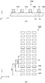
図2に示すように、キャリッジ103は、それぞれほぼ同じ構造を有する複数のヘッド114を保持している。本実施例では、キャリッジ103に保持されるヘッド114の数は24個である。それぞれのヘッド114は、後述する複数のノズル118が設けられた底面を有している。それぞれのヘッド114のこの底面の形状は、2つの長辺と2つの短辺とを有する多角形である。図2に示すように、キャリッジ103に保持されたヘッド114の底面はステージ106側を向いており、さらに、ヘッド114の長辺方向と短辺方向とは、それぞれX軸方向とY軸方向とに平行である。なお、ヘッド114同士の相対位置関係の詳細は、後述する。   As shown in FIG. 2, the carriage 103 holds a plurality of heads 114 each having substantially the same structure. In this embodiment, the number of heads 114 held by the carriage 103 is 24. Each head 114 has a bottom surface provided with a plurality of nozzles 118 described later. The shape of the bottom surface of each head 114 is a polygon having two long sides and two short sides. As shown in FIG. 2, the bottom surface of the head 114 held by the carriage 103 faces the stage 106, and the long side direction and the short side direction of the head 114 are the X-axis direction and the Y-axis direction, respectively. Parallel to Details of the relative positional relationship between the heads 114 will be described later.

本明細書では、Y軸方向に隣接する4つのヘッド114を「ヘッド群114G」と表記することもある。この表記によれば、図2のキャリッジ103は、6つのヘッド群114Gを保持していると表現し得る。   In the present specification, the four heads 114 adjacent in the Y-axis direction may be referred to as “head group 114G”. According to this notation, the carriage 103 in FIG. 2 can be expressed as holding six head groups 114G.

(C.ヘッド)
図3は、ヘッド114の底面を示す。ヘッド114は、X軸方向に並んだ複数のノズル118を有する。これら複数のノズル118は、ヘッド114のX軸方向のノズルピッチHXPが約70μmとなるように配置されている。ここで、「ヘッド114のX軸方向のノズルピッチHXP」は、ヘッド114におけるノズル118のすべてをY軸方向に沿ってX軸上に射像して得られた複数のノズル像間のピッチに相当する。
(C. Head)
FIG. 3 shows the bottom surface of the head 114. The head 114 has a plurality of nozzles 118 arranged in the X-axis direction. The plurality of nozzles 118 are arranged such that the nozzle pitch HXP in the X-axis direction of the head 114 is about 70 μm. Here, the “nozzle pitch HXP in the X-axis direction of the head 114” is a pitch between a plurality of nozzle images obtained by projecting all the nozzles 118 in the head 114 on the X-axis along the Y-axis direction. Equivalent to.

本実施例では、ヘッド114における複数のノズル118は、ともにX軸方向に延びるノズル列116Aと、ノズル列116Bと、をなす。ノズル列116Aと、ノズル列116Bとは、Y軸方向に隣合う。また、ノズル列116Aとノズル列116Bとの間の距離、つまりY軸方向の距離、はDAである。図3では、ノズル列116AのY座標が、ノズル列116BのY座標より大きい。そして、ノズル列116Aおよびノズル列116Bのそれぞれにおいて、90個のノズル118が一定間隔でX軸方向に一列に並んでいる。本実施例では、この一定間隔は約140μmである。つまり、ノズル列116AのノズルピッチLNPおよびノズル列116BのノズルピッチLNPは、ともに約140μmである。   In this embodiment, the plurality of nozzles 118 in the head 114 form a nozzle row 116A and a nozzle row 116B that extend in the X-axis direction. The nozzle row 116A and the nozzle row 116B are adjacent to each other in the Y-axis direction. Further, the distance between the nozzle row 116A and the nozzle row 116B, that is, the distance in the Y-axis direction is DA. In FIG. 3, the Y coordinate of the nozzle row 116A is larger than the Y coordinate of the nozzle row 116B. In each of the nozzle row 116A and the nozzle row 116B, 90 nozzles 118 are aligned in the X-axis direction at regular intervals. In this embodiment, this regular interval is about 140 μm. That is, the nozzle pitch LNP of the nozzle row 116A and the nozzle pitch LNP of the nozzle row 116B are both about 140 μm.

ノズル列116Bの位置は、ノズル列116Aの位置に対して、ノズルピッチLNPの半分の長さ(約70μm)だけX軸方向の正の方向(図3の右方向)にずれている。このため、ヘッド114のX軸方向のノズルピッチHXPは、ノズル列116A(またはノズル列116B)のノズルピッチLNPの半分の長さ(約70μm)である。   The position of the nozzle row 116B is shifted from the position of the nozzle row 116A in the positive direction in the X-axis direction (the right direction in FIG. 3) by half the nozzle pitch LNP (about 70 μm). Therefore, the nozzle pitch HXP in the X-axis direction of the head 114 is half the length (about 70 μm) of the nozzle pitch LNP of the nozzle row 116A (or nozzle row 116B).

したがって、ヘッド114のX軸方向のノズル線密度は、ノズル列116A(またはノズル列116B)のノズル線密度の2倍である。なお、本明細書において「X軸方向のノズル線密度」とは、複数のノズルをY軸方向に沿ってX軸上に射像して得られた複数のノズル像の単位長さ当たりの数に相当する。   Therefore, the nozzle line density in the X-axis direction of the head 114 is twice the nozzle line density of the nozzle row 116A (or nozzle row 116B). In the present specification, “nozzle line density in the X-axis direction” means the number per unit length of a plurality of nozzle images obtained by projecting a plurality of nozzles on the X-axis along the Y-axis direction. It corresponds to.

もちろん、ヘッド114が含むノズル列の数は、2つだけに限定されない。ヘッド114はM個のノズル列を含んでもよい。ここで、Mは1以上の自然数である。この場合には、M個のノズル列のそれぞれにおいて複数のノズル118は、ノズルピッチHXPのM倍の長さのピッチで並ぶ。さらに、Mが2以上の自然数の場合には、M個のノズル列のうちの一つに対して、他の(M−1)個のノズル列は、ノズルピッチHXPのi倍の長さだけ重複無くX軸方向にずれている。ここで、iは1から(M−1)までの自然数である。   Of course, the number of nozzle rows included in the head 114 is not limited to two. The head 114 may include M nozzle rows. Here, M is a natural number of 1 or more. In this case, in each of the M nozzle rows, the plurality of nozzles 118 are arranged at a pitch that is M times the nozzle pitch HXP. Further, when M is a natural number of 2 or more, the other (M−1) nozzle rows are only i times as long as the nozzle pitch HXP with respect to one of the M nozzle rows. There is no overlap in the X-axis direction. Here, i is a natural number from 1 to (M−1).

さて、ノズル列116Aおよびノズル列116Bのそれぞれが90個のノズル118からなるため、1つのヘッド114は180個のノズル118を有する。ただし、ノズル列116Aの両端のそれぞれ5ノズルは「休止ノズル」として設定されている。同様に、ノズル列116Bの両端のそれぞれ5ノズルも「休止ノズル」として設定されている。そして、これら20個の「休止ノズル」からは液状の材料111が吐出されない。このため、ヘッド114における180個のノズル118のうち、160個のノズル118が液状の材料111を吐出するノズルとして機能する。本明細書では、これら160個のノズル118を「吐出ノズル」と表記することもある。   Now, since each of the nozzle row 116 </ b> A and the nozzle row 116 </ b> B includes 90 nozzles 118, one head 114 has 180 nozzles 118. However, 5 nozzles at both ends of the nozzle row 116A are set as “pause nozzles”. Similarly, 5 nozzles at both ends of the nozzle row 116B are also set as “pause nozzles”. The liquid material 111 is not discharged from these 20 “pause nozzles”. Therefore, of the 180 nozzles 118 in the head 114, 160 nozzles 118 function as nozzles that discharge the liquid material 111. In the present specification, these 160 nozzles 118 may be referred to as “ejection nozzles”.

なお、1つのヘッド114におけるノズル118の数は、180個に限定されない。1つのヘッド114に360個のノズルが設けられていてもよい。この場合には、ノズル列116Aおよび116Bのそれぞれが、180個のノズル118からなればよい。また、本発明において吐出ノズルの数は、160個に限定されない。1つのヘッド114にP個の吐出ノズルがあってもよい。ここで、Pは2以上の自然数であって、ヘッド114における全ノズル数以下であればよい。   Note that the number of nozzles 118 in one head 114 is not limited to 180. One nozzle 114 may be provided with 360 nozzles. In this case, each of the nozzle arrays 116 </ b> A and 116 </ b> B only needs to include 180 nozzles 118. In the present invention, the number of discharge nozzles is not limited to 160. One head 114 may have P ejection nozzles. Here, P is a natural number equal to or greater than 2, and may be equal to or less than the total number of nozzles in the head 114.

本明細書では、ヘッド114同士の相対位置関係を説明する目的で、ノズル列116Aに含まれる90個のノズル118のうち、左から6番目のノズル118をヘッド114の「基準ノズル118R」と表記する。つまり、ノズル列116Aにおける80個の吐出ノズルのうち、最も左側の吐出ノズルがヘッド114の「基準ノズル118R」である。なお、すべてのヘッド114に対して、「基準ノズル118R」の指定の仕方が同じであればよいので、「基準ノズル118R」の位置は、上記位置でなくてもよい。   In the present specification, for the purpose of explaining the relative positional relationship between the heads 114, among the 90 nozzles 118 included in the nozzle row 116 </ b> A, the sixth nozzle 118 from the left is expressed as “reference nozzle 118 </ b> R” of the head 114. To do. That is, among the 80 discharge nozzles in the nozzle row 116A, the leftmost discharge nozzle is the “reference nozzle 118R” of the head 114. Note that the “reference nozzle 118R” may be specified in the same manner for all the heads 114, so the position of the “reference nozzle 118R” does not have to be the above position.

図4(a)および(b)に示すように、それぞれのヘッド114は、インクジェットヘッドである。より具体的には、それぞれのヘッド114は、振動板126と、ノズルプレート128と、を備えている。振動板126と、ノズルプレート128と、の間には、タンク101から孔131を介して供給される液状の材料111が常に充填される液たまり129が位置している。   As shown in FIGS. 4A and 4B, each head 114 is an inkjet head. More specifically, each head 114 includes a diaphragm 126 and a nozzle plate 128. Between the diaphragm 126 and the nozzle plate 128, a liquid pool 129 in which the liquid material 111 supplied from the tank 101 through the hole 131 is always filled is located.

また、振動板126と、ノズルプレート128と、の間には、複数の隔壁122が位置している。そして、振動板126と、ノズルプレート128と、1対の隔壁122と、によって囲まれた部分がキャビティ120である。キャビティ120はノズル118に対応して設けられているため、キャビティ120の数とノズル118の数とは同じである。キャビティ120には、1対の隔壁122間に位置する供給口130を介して、液たまり129から液状の材料111が供給される。   In addition, a plurality of partition walls 122 are located between the diaphragm 126 and the nozzle plate 128. A portion surrounded by the diaphragm 126, the nozzle plate 128, and the pair of partition walls 122 is a cavity 120. Since the cavities 120 are provided corresponding to the nozzles 118, the number of the cavities 120 and the number of the nozzles 118 are the same. The liquid material 111 is supplied from the liquid pool 129 to the cavity 120 via the supply port 130 positioned between the pair of partition walls 122.

振動板126上には、それぞれのキャビティ120に対応して、振動子124が位置する。振動子124は、ピエゾ素子124Cと、ピエゾ素子124Cを挟む1対の電極124A、124Bと、を含む。この1対の電極124A、124Bとの間に駆動電圧を与えることで、対応するノズル118から液状の材料111が吐出される。なお、ノズル118からZ軸方向に液状の材料111が吐出されるように、ノズル118の形状が調整されている。   On the diaphragm 126, the vibrator 124 is positioned corresponding to each cavity 120. The vibrator 124 includes a piezoelectric element 124C and a pair of electrodes 124A and 124B that sandwich the piezoelectric element 124C. By applying a driving voltage between the pair of electrodes 124A and 124B, the liquid material 111 is discharged from the corresponding nozzle 118. The shape of the nozzle 118 is adjusted so that the liquid material 111 is discharged from the nozzle 118 in the Z-axis direction.

ここで、本明細書において「液状の材料」とは、ノズルから吐出可能な粘度を有する材料をいう。この場合、材料が水性であると油性であるとを問わない。ノズルから吐出可能な流動性(粘度)を備えていれば十分で、固体物質が混入していても全体として流動体であればよい。   Here, the “liquid material” in this specification refers to a material having a viscosity that can be discharged from a nozzle. In this case, it does not matter whether the material is aqueous or oily. It is sufficient if it has fluidity (viscosity) that can be discharged from the nozzle, and even if a solid substance is mixed, it may be a fluid as a whole.

制御部112(図1)は、複数の振動子124のそれぞれに互いに独立に信号を与えるように構成されていてもよい。つまり、ノズル118から吐出される材料111の体積が、制御部112からの信号に応じてノズル118毎に制御されてもよい。そのような場合には、ノズル118のそれぞれから吐出される材料111の体積は、0pl〜42pl(ピコリットル)の間で可変にしてもよい。また、制御部112は、後述するように、塗布走査の間に吐出動作を行うノズル118と、吐出動作を行わないノズル118と、を設定することでもできる。   The control unit 112 (FIG. 1) may be configured to give a signal to each of the plurality of transducers 124 independently of each other. That is, the volume of the material 111 ejected from the nozzle 118 may be controlled for each nozzle 118 according to a signal from the control unit 112. In such a case, the volume of the material 111 discharged from each of the nozzles 118 may be variable between 0 pl to 42 pl (picoliter). Further, as will be described later, the control unit 112 can also set the nozzle 118 that performs the ejection operation during the application scan and the nozzle 118 that does not perform the ejection operation.

本明細書では、1つのノズル118と、ノズル118に対応するキャビティ120と、キャビティ120に対応する振動子124と、を含んだ部分を「吐出部127」と表記することもある。この表記によれば、1つのヘッド114は、ノズル118の数と同じ数の吐出部127を有する。吐出部127は、ピエゾ素子の代わりに電気熱変換素子を有してもよい。つまり、吐出部127は、電気熱変換素子による材料の熱膨張を利用して材料を吐出する構成を有していてもよい。   In this specification, a portion including one nozzle 118, a cavity 120 corresponding to the nozzle 118, and a vibrator 124 corresponding to the cavity 120 may be referred to as “ejection unit 127”. According to this notation, one head 114 has the same number of ejection units 127 as the number of nozzles 118. The discharge unit 127 may include an electrothermal conversion element instead of the piezo element. That is, the discharge unit 127 may have a configuration for discharging a material by utilizing thermal expansion of the material by the electrothermal conversion element.

(D.ヘッド群)
次に、ヘッド群114Gにおける4つのヘッド114の相対位置関係を説明する。図5には、図2のキャリッジ103においてY軸方向に隣接する2つのヘッド群114Gが示されている。
(D. Head group)
Next, the relative positional relationship of the four heads 114 in the head group 114G will be described. FIG. 5 shows two head groups 114G adjacent in the Y-axis direction in the carriage 103 of FIG.

図5に示すように、それぞれのヘッド群114Gは、4つのヘッド114からなる。そして、ヘッド群114GのX軸方向のノズルピッチGXPが、ヘッド114のX軸方向のノズルピッチHXPの1/4倍の長さとなるように、ヘッド群114において4つのヘッド114が配置されている。より具体的には、1つのヘッド114の基準ノズル118RのX座標に対して、他のヘッド114の基準ノズル118RのX座標が、ノズルピッチHXPのj/4倍の長さだけ、X軸方向に重複無くずれて位置している。ここで、jは1から3までの自然数である。このため、ヘッド群114GのX軸方向のノズルピッチGXPは、ノズルピッチHXPの1/4倍である。   As shown in FIG. 5, each head group 114 </ b> G includes four heads 114. The four heads 114 are arranged in the head group 114 so that the nozzle pitch GXP in the X-axis direction of the head group 114G is ¼ times the nozzle pitch HXP in the X-axis direction of the head 114. . More specifically, with respect to the X coordinate of the reference nozzle 118R of one head 114, the X coordinate of the reference nozzle 118R of the other head 114 is the length of j / 4 times the nozzle pitch HXP in the X-axis direction. Are located without any overlap. Here, j is a natural number from 1 to 3. For this reason, the nozzle pitch GXP in the X-axis direction of the head group 114G is 1/4 times the nozzle pitch HXP.

本実施例では、ヘッド114のX軸方向のノズルピッチHXPは約70μmだから、ヘッド群114GのX軸方向のノズルピッチGXPは、その1/4倍の約17.5μmである。ここで、「ヘッド群114GのX軸方向のノズルピッチGXP」は、ヘッド群114Gにおけるノズル118のすべてを、Y軸方向に沿ってX軸上に射像して得られた複数のノズル像間のピッチに相当する。   In the present embodiment, since the nozzle pitch HXP in the X-axis direction of the head 114 is about 70 μm, the nozzle pitch GXP in the X-axis direction of the head group 114G is about 17.5 μm, which is a quarter of that. Here, the “nozzle pitch GXP of the head group 114G in the X-axis direction” is the interval between a plurality of nozzle images obtained by projecting all the nozzles 118 in the head group 114G onto the X-axis along the Y-axis direction. It corresponds to the pitch.

もちろん、ヘッド群114Gが含むヘッド114の数は、4つだけに限定されない。ヘッド群114GはN個のヘッド114からなってもよい。ここで、Nは2以上の自然数である。この場合には、ノズルピッチGXPがノズルピッチHXPの1/N倍の長さになるように、ヘッド群114GにおいてN個のヘッド114が配置されればよい。あるいは、N個のヘッド114の一つにおける基準ノズル118RのX座標に対して、他の(N−1)個のヘッド114における基準ノズル118のX座標が、ノズルピッチHXPのj/N倍の長さだけ重複無くずれていればよい。なお、この場合には、jは1から(N−1)までの自然数である。   Of course, the number of heads 114 included in the head group 114G is not limited to four. The head group 114G may include N heads 114. Here, N is a natural number of 2 or more. In this case, N heads 114 may be arranged in the head group 114G so that the nozzle pitch GXP is 1 / N times as long as the nozzle pitch HXP. Alternatively, with respect to the X coordinate of the reference nozzle 118R in one of the N heads 114, the X coordinate of the reference nozzle 118 in the other (N−1) heads 114 is j / N times the nozzle pitch HXP. It suffices if the length is shifted without overlap. In this case, j is a natural number from 1 to (N−1).

以下では、本実施例のヘッド114の相対位置関係をより具体的に説明する。   Hereinafter, the relative positional relationship of the head 114 of this embodiment will be described more specifically.

まず、説明を平易にする目的で、図5の左上のヘッド群114Gに含まれる4つのヘッド114を、Y軸方向の負の方向(図5の下方向)に向かって、ヘッド1141、ヘッド1142、ヘッド1143、ヘッド1144と表記する。同様に、図5の右下のヘッド群114Gに含まれる4つのヘッド114を、上からそれぞれヘッド1145、ヘッド1146、ヘッド1147、ヘッド1148と表記する。   First, for the purpose of simplifying the description, the four heads 114 included in the upper left head group 114G in FIG. 5 are moved toward the negative direction in the Y-axis direction (downward in FIG. 5). , Head 1143 and head 1144. Similarly, the four heads 114 included in the lower right head group 114G in FIG. 5 are respectively expressed as a head 1145, a head 1146, a head 1147, and a head 1148 from the top.

そして、ヘッド1141におけるノズル列116A、116Bをノズル列1A、1Bと表記し、ヘッド1142におけるノズル列116A、116Bをノズル列2A、2Bと表記し、ヘッド1143におけるノズル列116A、116Bをノズル列3A、3Bと表記し、ヘッド1144におけるノズル列116A、116Bをノズル列4A、4Bと表記する。同様に、ヘッド1145におけるノズル列116A、116Bをノズル列5A、5Bと表記し、ヘッド1146におけるノズル列116A、116Bをノズル列6A、6Bと表記し、ヘッド1147におけるノズル列116A、116Bをノズル列7A、7Bと表記し、ヘッド1148におけるノズル列116A、116Bをノズル列8A、8Bと表記する。   The nozzle rows 116A and 116B in the head 1141 are denoted as nozzle rows 1A and 1B, the nozzle rows 116A and 116B in the head 1142 are denoted as nozzle rows 2A and 2B, and the nozzle rows 116A and 116B in the head 1143 are denoted as nozzle row 3A. 3B, and the nozzle rows 116A and 116B in the head 1144 are indicated as nozzle rows 4A and 4B. Similarly, the nozzle rows 116A and 116B in the head 1145 are denoted as nozzle rows 5A and 5B, the nozzle rows 116A and 116B in the head 1146 are denoted as nozzle rows 6A and 6B, and the nozzle rows 116A and 116B in the head 1147 are denoted as nozzle rows. 7A and 7B, and the nozzle arrays 116A and 116B in the head 1148 are expressed as nozzle arrays 8A and 8B.

これらノズル列1A〜8Bのそれぞれは、実際には90個のノズル118からなる。そして、上述したように、ノズル列1A〜8Bのそれぞれにおいて、これら90個のノズルは、X軸方向に並んでいる。ただし、図5では説明の便宜上、ノズル列1A〜8Bのそれぞれが、4つの吐出ノズル(ノズル118)からなるように描かれている。さらに、図5では、ノズル列1Aの最も左のノズル118がヘッド1141の基準ノズル118Rであり、ノズル列2Aの最も左のノズル118がヘッド1142の基準ノズル118Rであり、ノズル列3Aの最も左のノズル118がヘッド1143の基準ノズル118Rであり、ノズル列4Aの最も左のノズル118がヘッド1144の基準ノズル118Rであり、ノズル列5Aの最も左のノズル118がヘッド1145の基準ノズル118Rである。   Each of these nozzle arrays 1A to 8B actually includes 90 nozzles 118. And as above-mentioned, in each of nozzle row 1A-8B, these 90 nozzles are located in a line with the X-axis direction. However, in FIG. 5, for convenience of explanation, each of the nozzle rows 1 </ b> A to 8 </ b> B is drawn to include four discharge nozzles (nozzles 118). Further, in FIG. 5, the leftmost nozzle 118 of the nozzle row 1A is the reference nozzle 118R of the head 1141, the leftmost nozzle 118 of the nozzle row 2A is the reference nozzle 118R of the head 1142, and the leftmost nozzle of the nozzle row 3A. No. 118 is the reference nozzle 118R of the head 1143, the leftmost nozzle 118 of the nozzle row 4A is the reference nozzle 118R of the head 1144, and the leftmost nozzle 118 of the nozzle row 5A is the reference nozzle 118R of the head 1145. .

そして、ヘッド1142の基準ノズル118Rの位置(またはX座標)は、ヘッド1141の基準ノズル118Rの位置(またはX座標)から約17.5μmだけX軸方向の正の方向(図5の右方向)にずれている。そして、ヘッド1143の基準ノズル118Rの位置は、ヘッド1142の基準ノズル118Rの位置から約17.5μmだけX軸方向の正の方向にずれている。さらに、ヘッド1144の基準ノズル118Rの位置は、ヘッド1143の基準ノズル118Rの位置から約17.5μmだけX軸方向の正の方向にずれている。なお、あるヘッドが他のヘッドに対してずれる方向は、X軸方向の正の方向だけでなく、負の方向(図5の左方向)でもよい。   The position (or X coordinate) of the reference nozzle 118R of the head 1142 is about 17.5 μm from the position (or X coordinate) of the reference nozzle 118R of the head 1141 in the positive direction in the X axis direction (the right direction in FIG. 5). It is shifted to. The position of the reference nozzle 118R of the head 1143 is shifted from the position of the reference nozzle 118R of the head 1142 by about 17.5 μm in the positive direction of the X axis direction. Furthermore, the position of the reference nozzle 118R of the head 1144 is shifted from the position of the reference nozzle 118R of the head 1143 by about 17.5 μm in the positive direction in the X-axis direction. Note that the direction in which a certain head is displaced with respect to another head may be not only the positive direction in the X-axis direction but also the negative direction (left direction in FIG. 5).

上記配置によって、ノズル列1Aの最も左のノズル118のX座標とノズル列1Bの最も左のノズル118のX座標との間に、ノズル列2Aの最も左のノズル118のX座標と、ノズル列3Aの最も左のノズル118のX座標と、ノズル列4Aの最も左のノズル118のX座標と、が収まる。同様に、ノズル列1Bの最も左のノズル118のX座標とノズル列1Aの左から2番目のノズル118のX座標との間に、ノズル列2Bの最も左のノズル118のX座標と、ノズル列3Bの最も左のノズル118のX座標と、ノズル列4Bの最も左のノズル118のX座標と、が収まる。ノズル列1Aの他のノズル118のX座標と、ノズル列1Bの他のノズル118のX座標と、の間にも、同様にノズル列2A(または2B)のノズル118のX座標、ノズル列3A(または3B)のノズル118のX座標、ノズル列4A(または4B)のノズル118のX座標が収まる。   With the above arrangement, the X coordinate of the leftmost nozzle 118 in the nozzle row 2A and the X coordinate of the leftmost nozzle 118 in the nozzle row 1B are between the X coordinate of the leftmost nozzle 118 in the nozzle row 1A and the X coordinate of the leftmost nozzle 118 in the nozzle row 1B. The X coordinate of the leftmost nozzle 118 of 3A and the X coordinate of the leftmost nozzle 118 of the nozzle row 4A are accommodated. Similarly, between the X coordinate of the leftmost nozzle 118 of the nozzle row 1B and the X coordinate of the second nozzle 118 from the left of the nozzle row 1A, the X coordinate of the leftmost nozzle 118 of the nozzle row 2B and the nozzle The X coordinate of the leftmost nozzle 118 in the row 3B and the X coordinate of the leftmost nozzle 118 in the nozzle row 4B fit. Similarly, between the X coordinate of the other nozzle 118 in the nozzle row 1A and the X coordinate of the other nozzle 118 in the nozzle row 1B, the X coordinate of the nozzle 118 in the nozzle row 2A (or 2B), the nozzle row 3A The X coordinate of the nozzle 118 in (or 3B) and the X coordinate of the nozzle 118 in the nozzle row 4A (or 4B) are contained.

本実施例では、ヘッド1141の基準ノズル118RのX座標に対して、ヘッド1142、1143、1144の基準ノズルのX座標が、ノズルピッチHXPの1/4倍の長さ、ノズルピッチHXPの2/4倍の長さ、ノズルピッチHXPの3/4倍の長さだけそれぞれずれている。しかしながら、4つのヘッド114の配置はこのような配置に限定されず、1つのヘッド114の基準ノズル118RのX座標に対して、他のヘッドの基準ノズル118RのX座標が、ノズルピッチHXPのj/4倍の長さだけX軸方向に重複無くずれて位置していればよい。ここで、jは1から3までの自然数である。   In this embodiment, the X coordinate of the reference nozzles of the heads 1142, 1143, and 1144 is ¼ times the nozzle pitch HXP and 2 / nozzle pitch HXP with respect to the X coordinate of the reference nozzle 118R of the head 1141. They are shifted by 4 times the length and 3/4 times the nozzle pitch HXP. However, the arrangement of the four heads 114 is not limited to such an arrangement, and the X coordinate of the reference nozzle 118R of the other head is j of the nozzle pitch HXP with respect to the X coordinate of the reference nozzle 118R of one head 114. It suffices if the position is shifted in the X-axis direction without overlap by a length of / 4 times. Here, j is a natural number from 1 to 3.

図5の右下のヘッド群114Gにおけるヘッド1145、1146、1147、1148の配置、つまりコンフィギュレーションも、ヘッド1141、1142、1143、1144の配置と同様である。   The arrangement of the heads 1145, 1146, 1147, and 1148, that is, the configuration in the lower right head group 114G in FIG. 5 is the same as the arrangement of the heads 1141, 1142, 1143, and 1144.

X軸方向に互いに隣接する2つのヘッド群114Gの間の相対位置関係を、ヘッド1145とヘッド1141との間の相対位置関係に基づいて説明する。   The relative positional relationship between the two head groups 114G adjacent to each other in the X-axis direction will be described based on the relative positional relationship between the head 1145 and the head 1141.

ヘッド1145の基準ノズル118Rの位置は、ヘッド1141の基準ノズル118Rの位置から、ヘッド114のX軸方向のノズルピッチHXPと、ヘッド114における吐出ノズルの数と、の積の長さだけX軸方向の正の方向にずれている。本実施例では、ノズルピッチHXPは約70μmであるとともに、1つのヘッド114における吐出ノズルの数は160個なので、ヘッド1145の基準ノズル118Rの位置は、ヘッド1141の基準ノズル118Rの位置から11.2mm(70μm×160)だけX軸方向の正の方向にずれている。ただし、図5では、説明の便宜上、ヘッド1141における吐出ノズルの数は8個なので、ヘッド1145の基準ノズル118Rの位置が、ヘッド1141の基準ノズル1141の位置から560μm(70μm×8)だけX軸方向にずれているように描かれている。   The position of the reference nozzle 118R of the head 1145 is the X-axis direction from the position of the reference nozzle 118R of the head 1141 by the product length of the nozzle pitch HXP in the X-axis direction of the head 114 and the number of ejection nozzles in the head 114. It is shifted in the positive direction. In this embodiment, the nozzle pitch HXP is about 70 μm, and the number of ejection nozzles in one head 114 is 160. Therefore, the position of the reference nozzle 118R of the head 1145 is 11.1 from the position of the reference nozzle 118R of the head 1141. It is shifted in the positive direction along the X axis by 2 mm (70 μm × 160). However, in FIG. 5, for convenience of explanation, since the number of ejection nozzles in the head 1141 is 8, the position of the reference nozzle 118R of the head 1145 is 560 μm (70 μm × 8) from the position of the reference nozzle 1141 of the head 1141 on the X axis. It is drawn so as to be out of direction.

ヘッド1141とヘッド1145とが上述のように配置されているので、ノズル列1Aの最も右の吐出ノズルのX座標と、ノズル列5Aの最も左の吐出ノズルのX座標とは、ノズルピッチLNPだけずれている。このため、2つのヘッド114G全体のX軸方向のノズルピッチは、ヘッド114のX軸方向のノズルピッチHXPの1/4倍である。   Since the head 1141 and the head 1145 are arranged as described above, the X coordinate of the rightmost discharge nozzle of the nozzle row 1A and the X coordinate of the leftmost discharge nozzle of the nozzle row 5A are only the nozzle pitch LNP. It's off. For this reason, the nozzle pitch in the X-axis direction of the two heads 114G as a whole is 1/4 times the nozzle pitch HXP in the X-axis direction of the head 114.

また、キャリッジ103全体としてのX軸方向のノズルピッチも、17.5μm、すなわち、ヘッド114のX軸方向のノズルピッチHXPの1/4倍の長さになるように、6つのヘッド群114Gが配置されている。   In addition, the six head groups 114G are arranged so that the nozzle pitch in the X-axis direction as a whole of the carriage 103 is also 17.5 μm, that is, 1/4 times the nozzle pitch HXP in the X-axis direction of the head 114. Has been placed.

さらに本実施例では、複数のヘッド114(図5では1141〜1148)のそれぞれにおいて、ノズル列116Aとノズル列116Bとの間の距離はDAである。なお、図3において説明したように、ノズル列116AのY座標は、ノズル列116BのY座標より大きい。ここで、本明細書では、1つのヘッド114におけるノズル列116Aとノズル列116Bとの間の距離を、「第1のノズル列間距離DA」と表記する。   Further, in this embodiment, in each of the plurality of heads 114 (1141 to 1148 in FIG. 5), the distance between the nozzle row 116A and the nozzle row 116B is DA. As described in FIG. 3, the Y coordinate of the nozzle row 116A is larger than the Y coordinate of the nozzle row 116B. Here, in this specification, the distance between the nozzle row 116A and the nozzle row 116B in one head 114 is referred to as “first nozzle row distance DA”.

一方、任意の一つのヘッド114におけるノズル列116Bと、その任意の一つのヘッドにY軸方向に隣合うヘッド114におけるノズル列116Aとの間の距離は、DBである。本明細書では、この距離を「第2のノズル列間距離DB」と表記する。図5の場合には、ヘッド1141におけるノズル列116B(図5では1B)と、ヘッド1142におけるノズル列116A(図5では列2A)との間の距離がDBである。さらに、ヘッド1142におけるノズル列116B(図5ではノズル列2B)と、ヘッド1143におけるノズル列116A(図5ではノズル列3A)との間の距離もDBである。同様に、ノズル列3Bとノズル列4Aとの間の距離、およびノズル列4Bとノズル列5Aとの間の距離もDBである。   On the other hand, the distance between the nozzle row 116B in any one head 114 and the nozzle row 116A in the head 114 adjacent to the arbitrary one head in the Y-axis direction is DB. In this specification, this distance is referred to as “second nozzle row distance DB”. In the case of FIG. 5, the distance between the nozzle row 116B (1B in FIG. 5) in the head 1141 and the nozzle row 116A (row 2A in FIG. 5) in the head 1142 is DB. Further, the distance between the nozzle row 116B in the head 1142 (nozzle row 2B in FIG. 5) and the nozzle row 116A in the head 1143 (nozzle row 3A in FIG. 5) is also DB. Similarly, the distance between the nozzle row 3B and the nozzle row 4A and the distance between the nozzle row 4B and the nozzle row 5A are also DB.

本実施例では、第2のノズル列間距離DBが第1のノズル列間距離DAのほぼ整数倍になるように、ヘッド群114Gにおいて4つのヘッド114が配置されている。例えば、ノズル列1Bとノズル列2Aとの間の距離は、第1のノズル列間距離DAのほぼ整数倍である。さらに、ヘッド1141、1142の配置において、ノズル列1Bとノズル列2Aとの間の距離が第1のノズル列間距離DAのほぼ整数倍なので、ノズル列1Aとノズル列2Aとの間の距離も、ノズル列1Bとノズル列2Bとの間の距離も、ノズル列1Aとノズル列2Bとの間の距離も、第1のノズル列間距離DAのほぼ整数倍である。   In the present embodiment, the four heads 114 are arranged in the head group 114G so that the second inter-nozzle row distance DB is approximately an integral multiple of the first inter-nozzle row distance DA. For example, the distance between the nozzle row 1B and the nozzle row 2A is substantially an integral multiple of the first nozzle row distance DA. Further, in the arrangement of the heads 1141 and 1142, the distance between the nozzle row 1B and the nozzle row 2A is almost an integral multiple of the first nozzle row distance DA, so the distance between the nozzle row 1A and the nozzle row 2A is also The distance between the nozzle row 1B and the nozzle row 2B and the distance between the nozzle row 1A and the nozzle row 2B are both approximately an integral multiple of the first nozzle row distance DA.

Y軸方向に互いに隣合う他の2つのヘッドの配置におけるノズル列間の距離も、ヘッド1141、1142の配置におけるノズル列間の距離と同様である。つまり、Y軸方向に隣合う2つのヘッドの一方における一つのノズル列と、他方のヘッドにおける一つのノズル列との間のY軸方向の距離が、第1のノズル列間距離の整数倍である。   The distance between the nozzle rows in the arrangement of the other two heads adjacent to each other in the Y-axis direction is the same as the distance between the nozzle rows in the arrangement of the heads 1141 and 1142. That is, the distance in the Y-axis direction between one nozzle row in one of the two heads adjacent in the Y-axis direction and one nozzle row in the other head is an integral multiple of the distance between the first nozzle rows. is there.

(E.制御部)
次に、制御部112の構成を説明する。図6に示すように、制御部112は、入力バッファメモリ200と、記憶手段202と、処理部204と、走査駆動部206と、ヘッド駆動部208と、を備えている。バッファメモリ202と処理部204とは相互に通信可能に接続されている。処理部204と記憶手段202とは、相互に通信可能に接続されている。処理部204と走査駆動部206とは相互に通信可能に接続されている。処理部204とヘッド駆動部20とは相互に通信可能に接続されている。また、走査駆動部206は、第1位置制御手段104および第2位置制御手段108と相互に通信可能に接続されている。同様にヘッド駆動部208は、複数のヘッド114のそれぞれと相互に通信可能に接続されている。
(E. Control part)
Next, the configuration of the control unit 112 will be described. As shown in FIG. 6, the control unit 112 includes an input buffer memory 200, a storage unit 202, a processing unit 204, a scan driving unit 206, and a head driving unit 208. The buffer memory 202 and the processing unit 204 are connected so that they can communicate with each other. The processing unit 204 and the storage unit 202 are connected to be communicable with each other. The processing unit 204 and the scan driving unit 206 are connected so as to communicate with each other. The processing unit 204 and the head driving unit 20 are connected so as to communicate with each other. Further, the scanning drive unit 206 is connected to the first position control unit 104 and the second position control unit 108 so as to communicate with each other. Similarly, the head driving unit 208 is connected to each of the plurality of heads 114 so as to communicate with each other.

入力バッファメモリ200は、外部情報処理装置から液状の材料111の液滴の吐出を行うための吐出データを受け取る。吐出データは、基体上のすべての被吐出部の相対位置を表すデータと、すべての被吐出部に液状の材料111を所望の厚さにまで塗布するのに必要となる相対走査の回数を示すデータと、オンノズル118Aとして機能するノズル118を指定するデータと、オフノズル118Bとして機能するノズル118を指定するデータと、を含む。オンノズル118Aおよびオフノズル118Bの説明は後述する。入力バッファメモリ200は、吐出データを処理部204に供給し、処理部204は吐出データを記憶手段202に格納する。図6では、記憶手段202はRAMである。   The input buffer memory 200 receives ejection data for ejecting droplets of the liquid material 111 from the external information processing apparatus. The ejection data indicates data representing the relative positions of all the ejected parts on the substrate and the number of relative scans required to apply the liquid material 111 to all the ejected parts to a desired thickness. Data, data specifying the nozzle 118 functioning as the on-nozzle 118A, and data specifying the nozzle 118 functioning as the off-nozzle 118B. The on-nozzle 118A and the off-nozzle 118B will be described later. The input buffer memory 200 supplies the ejection data to the processing unit 204, and the processing unit 204 stores the ejection data in the storage unit 202. In FIG. 6, the storage means 202 is a RAM.

処理部204は、記憶手段202内の吐出データに基づいて、被吐出部に対するノズル118の相対位置を示すデータを走査駆動部206に与える。走査駆動部206はこのデータと、後述する吐出周期EP(図7)と、に応じた駆動信号を第1位置制御手段104および第2位置制御手段108に与える。この結果、被吐出部に対してヘッド114が相対走査する。一方、処理部204は、記憶手段202に記憶された吐出データと、吐出周期EPと、に基づいて、吐出タイミング毎のノズル118のオン・オフを指定する選択信号SCをヘッド駆動部208へ与える。ヘッド駆動部208は、選択信号SCに基づいて、液状の材料111の吐出に必要な吐出信号ESをヘッド114に与える。この結果、ヘッド114における対応するノズル118から、液状の材料111が液滴として吐出される。   The processing unit 204 gives data indicating the relative position of the nozzle 118 to the discharge target unit to the scan driving unit 206 based on the discharge data in the storage unit 202. The scanning drive unit 206 supplies the first position control means 104 and the second position control means 108 with a drive signal corresponding to this data and an ejection period EP (FIG. 7) described later. As a result, the head 114 performs relative scanning with respect to the discharge target portion. On the other hand, the processing unit 204 gives a selection signal SC for designating ON / OFF of the nozzle 118 at each ejection timing to the head driving unit 208 based on the ejection data stored in the storage unit 202 and the ejection cycle EP. . The head driving unit 208 gives the head 114 an ejection signal ES necessary for ejecting the liquid material 111 based on the selection signal SC. As a result, the liquid material 111 is discharged as droplets from the corresponding nozzle 118 in the head 114.

制御部112は、CPU、ROM、RAMを含んだコンピュータであってもよい。この場合には、制御部112の上記機能は、コンピュータによって実行されるソフトウェアプログラムによって実現される。もちろん、制御部112は、専用の回路(ハードウェア)によって実現されてもよい。   The control unit 112 may be a computer including a CPU, a ROM, and a RAM. In this case, the function of the control unit 112 is realized by a software program executed by a computer. Of course, the control unit 112 may be realized by a dedicated circuit (hardware).

次に制御部112におけるヘッド駆動部208の構成と機能を説明する。   Next, the configuration and function of the head drive unit 208 in the control unit 112 will be described.

図7(a)に示すように、ヘッド駆動部208は、1つの駆動信号生成部203と、複数のアナログスイッチASと、を有する。図7(b)に示すように、駆動信号生成部203は駆動信号DSを生成する。駆動信号DSの電位は、基準電位Lに対して時間的に変化する。具体的には、駆動信号DSは、吐出周期EPで繰り返される複数の吐出波形Pを含む。ここで、吐出波形Pは、ノズル118から1つの液滴を吐出するために、対応する振動子124の一対の電極間に印加されるべき駆動電圧波形に対応する。   As shown in FIG. 7A, the head drive unit 208 includes one drive signal generation unit 203 and a plurality of analog switches AS. As shown in FIG. 7B, the drive signal generation unit 203 generates a drive signal DS. The potential of the drive signal DS changes with respect to the reference potential L over time. Specifically, the drive signal DS includes a plurality of ejection waveforms P that are repeated at the ejection cycle EP. Here, the discharge waveform P corresponds to a drive voltage waveform to be applied between a pair of electrodes of the corresponding vibrator 124 in order to discharge one droplet from the nozzle 118.

駆動信号DSは、アナログスイッチASのそれぞれの入力端子に供給される。アナログスイッチASのそれぞれは、吐出部127のそれぞれに対応して設けられている。つまり、アナログスイッチASの数と吐出部127の数(つまりノズル118の数)とは同じである。   The drive signal DS is supplied to each input terminal of the analog switch AS. Each of the analog switches AS is provided corresponding to each of the ejection units 127. That is, the number of analog switches AS and the number of ejection units 127 (that is, the number of nozzles 118) are the same.

処理部204は、ノズル118のオン・オフを表す選択信号SCを、アナログスイッチASのそれぞれに与える。ここで、選択信号SCは、アナログスイッチAS毎に独立にハイレベルおよびローレベルのどちらかの状態を取り得る。一方、アナログスイッチASは、駆動信号DSと選択信号SCとに応じて、振動子124の電極124Aに吐出信号ESを供給する。具体的には、選択信号SCがハイレベルの場合には、アナログスイッチASは電極124Aに吐出信号ESとして駆動信号DSを伝播する。一方、選択信号SCがローレベルの場合には、アナログスイッチASが出力する吐出信号ESの電位は基準電位Lとなる。振動子124の電極124Aに駆動信号DSが与えられると、その振動子124に対応するノズル118から液状の材料111が吐出される。なお、それぞれの振動子124の電極124Bには基準電位Lが与えられている。   The processing unit 204 gives a selection signal SC indicating ON / OFF of the nozzle 118 to each analog switch AS. Here, the selection signal SC can take either a high level or a low level independently for each analog switch AS. On the other hand, the analog switch AS supplies the ejection signal ES to the electrode 124A of the vibrator 124 according to the drive signal DS and the selection signal SC. Specifically, when the selection signal SC is at a high level, the analog switch AS propagates the drive signal DS as the ejection signal ES to the electrode 124A. On the other hand, when the selection signal SC is at a low level, the potential of the ejection signal ES output from the analog switch AS becomes the reference potential L. When the drive signal DS is given to the electrode 124A of the vibrator 124, the liquid material 111 is discharged from the nozzle 118 corresponding to the vibrator 124. A reference potential L is applied to the electrode 124B of each vibrator 124.

図7(b)に示す例では、2つの吐出信号ESのそれぞれにおいて、吐出周期EPの2倍の周期2EPで吐出波形Pが現れるように、2つの選択信号SCのそれぞれにおいてハイレベルの期間とローレベルの期間とが設定されている。これによって、対応する2つのノズル118のそれぞれから、周期2EPで液状の材料111が吐出される。また、これら2つのノズル118に対応する振動子124のそれぞれには、共通の駆動信号生成部203からの共通の駆動信号DSが与えられている。このため、2つのノズル118からほぼ同じタイミングで液状の材料111が吐出される。   In the example shown in FIG. 7B, a high-level period is set in each of the two selection signals SC so that the discharge waveform P appears in the cycle 2EP that is twice the discharge cycle EP in each of the two discharge signals ES. A low-level period is set. As a result, the liquid material 111 is discharged from each of the two corresponding nozzles 118 with a period of 2EP. A common drive signal DS from the common drive signal generation unit 203 is given to each of the vibrators 124 corresponding to these two nozzles 118. For this reason, the liquid material 111 is discharged from the two nozzles 118 at substantially the same timing.

以上の構成によって、吐出装置100は、制御部112に与えられた吐出データに応じて、液状の材料111の塗布走査を行う。   With the above configuration, the ejection device 100 performs application scanning of the liquid material 111 in accordance with ejection data given to the control unit 112.

(F.吐出方法の一例)
図8(a)および(b)を参照しながら、X軸方向に平行なストライプ状のターゲット、すなわち被吐出部18L、に対して、吐出装置100が液状の材料111を吐出する方法を説明する。具体的には、ヘッド群114Gまたはキャリッジ103における任意の一つのヘッドにおける第2のノズル列と、この任意の一つのヘッドに隣合うヘッドにおける第1のノズル列と、の間の距離を第1のノズル列間距離DAのほぼ整数倍に維持しながら、キャリッジ103をステージ106に対してY軸方向に相対移動させるステップを含んだ、液状の材料の塗布方法を説明する。
(F. Example of discharge method)
With reference to FIGS. 8A and 8B, description will be given of a method in which the discharge device 100 discharges the liquid material 111 to the stripe-shaped target parallel to the X-axis direction, that is, the discharged portion 18L. . Specifically, the distance between the second nozzle row in any one head in the head group 114G or the carriage 103 and the first nozzle row in the head adjacent to this one head is set to the first distance. A method for applying a liquid material, including the step of moving the carriage 103 relative to the stage 106 in the Y-axis direction while maintaining the distance between the nozzle rows DA of approximately an integer, will be described.

なお、図8(a)に示す例では、キャリッジ103のY軸方向への相対移動によって、図5で説明したヘッド1141、1142、1143、1144、1145が、この順番で被吐出部18Lと重なり合う。   In the example shown in FIG. 8A, the heads 1141, 1142, 1143, 1144, and 1145 described with reference to FIG. 5 overlap the ejected portion 18L in this order due to the relative movement of the carriage 103 in the Y-axis direction. .

図5を参照しながら説明したように、本実施例では、第2のノズル列間距離DBは、第1のノズル列間距離DAのほぼ整数倍である。つまり、
DB=c・DA…(式1)
である。ここで、cは、整数である。
As described with reference to FIG. 5, in the present embodiment, the second inter-nozzle row distance DB is substantially an integer multiple of the first inter-nozzle row distance DA. That means
DB = c 1 · DA (Formula 1)
It is. Here, c 1 is an integer.

本実施例では、ステージ106に対するキャリッジ103の相対移動速度Vは、
V=DA/(c・EP)…(式2)
となるように設定されている。ここで、DAは第1のノズル列間距離であり、EPは図7で示した吐出周期であり、cは整数である。
In this embodiment, the relative movement speed V of the carriage 103 with respect to the stage 106 is
V = DA / (c 2 · EP) (Formula 2)
It is set to become. Here, DA is the distance between the first nozzle row, EP is the discharge cycle shown in FIG. 7, c 2 is an integer.

相対移動速度Vが上記(式2)を満足するので、吐出周期EPの整数(c)倍の時間間隔で、ノズル列1Aとノズル列1B(図5)とが被吐出部18Lに重なる。しかも、本実施例では、第2のノズル列間距離DBは、第1のノズル列間距離DAの整数(c)倍だから、ノズル列1Bが被吐出部18Lに重なった時点から吐出周期EPの整数(c・c)倍の時間間隔で、ノズル列2A(図5)が被吐出部18Lに重なる。同様に、ヘッド群114Gにおけるすべてのノズル列が吐出周期EPの整数倍の時間間隔で被吐出部18Lに重なる。 Since the relative movement speed V satisfies the above (Formula 2), the nozzle row 1A and the nozzle row 1B (FIG. 5) overlap the discharged portion 18L at a time interval that is an integer (c 2 ) times the discharge period EP. In addition, in the present embodiment, the second nozzle row distance DB is an integer (c 1 ) times the first nozzle row distance DA, so that the discharge period EP starts from the point when the nozzle row 1B overlaps the discharged portion 18L. The nozzle row 2A (FIG. 5) overlaps the discharged portion 18L at a time interval that is an integer times (c 1 · c 2 ) times as large as. Similarly, all the nozzle rows in the head group 114G overlap the ejected portion 18L at a time interval that is an integral multiple of the ejection cycle EP.

したがって、すべてのノズル列が、吐出周期EPに関して同位相で被吐出部18Lに重なる、あるいは、被吐出部18Lに対応する領域に侵入する。このため、すべてのノズル列におけるノズル118に対して、駆動信号生成部203を共通にできる。このため、吐出波形(駆動波形)の精度を維持しつつ、回路構成をシンプルにすることができる。   Accordingly, all the nozzle rows overlap with the discharged portion 18L in the same phase with respect to the discharge period EP, or enter the region corresponding to the discharged portion 18L. For this reason, the drive signal generation unit 203 can be made common to the nozzles 118 in all the nozzle rows. For this reason, the circuit configuration can be simplified while maintaining the accuracy of the ejection waveform (drive waveform).

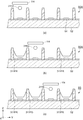
図8(a)に示すように、まず、キャリッジ103がステージ106に対してY軸方向に相対移動し始める。そして、ノズル列1Aが被吐出部18Lに重なると、ノズル列1Aに含まれるノズル118から、被吐出部18Lに対して材料111が同時に吐出される。図8(b)のラベル「1A」の右には、ノズル列1Aの吐出による着弾位置が黒丸で描かれている。図8(b)に示すように、ノズル列1Aの吐出によって、X軸方向にほぼ140μmのピッチで液状の材料111が被吐出部18Lに着弾する。   As shown in FIG. 8A, first, the carriage 103 starts to move relative to the stage 106 in the Y-axis direction. When the nozzle row 1A overlaps the discharged portion 18L, the material 111 is simultaneously discharged from the nozzles 118 included in the nozzle row 1A to the discharged portion 18L. On the right side of the label “1A” in FIG. 8B, the landing position by the ejection of the nozzle row 1A is drawn with a black circle. As shown in FIG. 8B, the liquid material 111 lands on the discharged portion 18L at a pitch of approximately 140 μm in the X-axis direction by the discharge of the nozzle row 1A.

ノズル列1Aが被吐出部18Lに重なった時点から吐出周期EPの整数倍(c倍)の時間期間後に、ノズル列1Bが被吐出部18Lに重なる。ノズル列1Bが被吐出部18Lに重なると、ノズル列1Bに含まれるノズル118から、被吐出部18Lに対して液状の材料111が同時に吐出される。図8(b)のラベル「1B」の右には、ノズル列1Bの吐出による着弾位置が黒丸で描かれている。図8(b)に示すように、ノズル列1Bの吐出によって、X軸方向にほぼ140μmのピッチで液状の材料111が被吐出部18Lに着弾する。ただし、ノズル列1Bの吐出による着弾位置と、ノズル列1Bに先行するノズル列1Aの吐出による着弾位置との間の距離は、ほぼ70μmである。なお、図8(b)のラベル「1B」の右には、ノズル列1Bに先行するノズル列の吐出による着弾位置が白丸で描かれている。 After a time period that is an integral multiple (c 2 times) of the discharge period EP from the time when the nozzle row 1A overlaps the discharged portion 18L, the nozzle row 1B overlaps the discharged portion 18L. When the nozzle row 1B overlaps the target portion 18L, the liquid material 111 is simultaneously discharged from the nozzles 118 included in the nozzle row 1B to the target portion 18L. On the right side of the label “1B” in FIG. 8B, the landing position by the ejection of the nozzle row 1B is drawn with a black circle. As shown in FIG. 8B, the liquid material 111 lands on the discharged portion 18L at a pitch of approximately 140 μm in the X-axis direction by the discharge of the nozzle row 1B. However, the distance between the landing position due to ejection of the nozzle row 1B and the landing position due to ejection of the nozzle row 1A preceding the nozzle row 1B is approximately 70 μm. Note that, on the right side of the label “1B” in FIG. 8B, the landing position by the ejection of the nozzle row preceding the nozzle row 1B is drawn with a white circle.

ノズル列1Bが被吐出部18Lに重なった時点から吐出周期EPの整数倍(c・c倍)の時間期間後に、ノズル列2Aが被吐出部18Lに重なる。ノズル列2Aが被吐出部18Lに重なると、ノズル列2Aに含まれるノズル118から、被吐出部18Lに対して液状の材料111が同時に吐出される。図8(b)のラベル「2A」の右には、ノズル列2Aの吐出による着弾位置が黒丸で描かれている。図8(b)に示すように、ノズル列2Aの吐出によって、X軸方向にほぼ140μmのピッチで液状の材料111が被吐出部18Lに着弾する。ただし、ノズル列2Aの吐出による着弾位置と、ノズル列2Aに先行するノズル列の吐出による着弾位置との間の最短距離は、ほぼ17.5μmである。なお、図8(b)のラベル「2A」の右には、ノズル列2Aに先行するノズル列による着弾位置が白丸で描かれている。 After a time period that is an integral multiple (c 1 · c 2 times) of the discharge period EP from the time when the nozzle row 1B overlaps the discharged portion 18L, the nozzle row 2A overlaps the discharged portion 18L. When the nozzle row 2A overlaps the discharged portion 18L, the liquid material 111 is simultaneously discharged from the nozzles 118 included in the nozzle row 2A to the discharged portion 18L. On the right side of the label “2A” in FIG. 8B, the landing position by the ejection of the nozzle row 2A is drawn with a black circle. As shown in FIG. 8B, the liquid material 111 lands on the discharged portion 18L at a pitch of approximately 140 μm in the X-axis direction by the discharge of the nozzle row 2A. However, the shortest distance between the landing position by the discharge of the nozzle row 2A and the landing position by the discharge of the nozzle row preceding the nozzle row 2A is approximately 17.5 μm. The landing position by the nozzle row preceding the nozzle row 2A is drawn with a white circle on the right side of the label “2A” in FIG. 8B.

ノズル列2Aが被吐出部18Lに重なった時点から吐出周期EPの整数倍(c倍)の時間期間後に、ノズル列2Bが被吐出部18Lに重なる。ノズル列2Bが被吐出部18Lに重なると、ノズル列2Bに含まれるノズル118から、被吐出部18Lに対して液状の材料111が同時に吐出される。図8(b)のラベル「2B」の右には、ノズル列2Bの吐出による着弾位置が黒丸で描かれている。図8(b)に示すように、ノズル列2Bの吐出によって、X軸方向にほぼ140μmのピッチで液状の材料が被吐出部18Lに着弾する。ただし、ノズル列2Bの吐出による着弾位置と、ノズル列2Bに先行するノズル列の吐出による着弾位置との間の最短距離は、ほぼ17.5μmである。なお、図8(b)のラベル「2B」の右には、ノズル列2Bに先行するノズル列の吐出による着弾位置が白丸で描かれている。 After a time period that is an integral multiple (c 2 times) of the discharge period EP from the time when the nozzle row 2A overlaps the discharged portion 18L, the nozzle row 2B overlaps the discharged portion 18L. When the nozzle row 2B overlaps the discharged portion 18L, the liquid material 111 is simultaneously discharged from the nozzles 118 included in the nozzle row 2B to the discharged portion 18L. On the right side of the label “2B” in FIG. 8B, the landing position by the ejection of the nozzle row 2B is drawn by a black circle. As shown in FIG. 8B, the liquid material lands on the discharged portion 18L at a pitch of approximately 140 μm in the X-axis direction by the discharge of the nozzle row 2B. However, the shortest distance between the landing position by the discharge of the nozzle row 2B and the landing position by the discharge of the nozzle row preceding the nozzle row 2B is approximately 17.5 μm. Note that, on the right side of the label “2B” in FIG. 8B, the landing position by the ejection of the nozzle row preceding the nozzle row 2B is drawn with a white circle.

その後、ノズル列3A、3B、4A、4B、5A、5Bがこの順番で被吐出部18Lに重なり、ノズル列3A、3B、4A、4B、5A、5Bのそれぞれから被吐出部18Lに対して、ノズル列1A、1B、2A、2Bと同様に液状の材料111が吐出される。この結果、ヘッド群114Gが被吐出部18Lに対してY軸方向に1回だけ相対移動する間に、ヘッド114のX軸方向のノズルピッチHXPの1/4倍の長さ、すなわち17.5μm、のピッチで液状の材料111が着弾する。   Thereafter, the nozzle rows 3A, 3B, 4A, 4B, 5A, and 5B overlap the ejected portion 18L in this order, and each of the nozzle rows 3A, 3B, 4A, 4B, 5A, and 5B is directed to the ejected portion 18L. The liquid material 111 is discharged in the same manner as the nozzle rows 1A, 1B, 2A, and 2B. As a result, while the head group 114G moves relative to the ejected portion 18L only once in the Y-axis direction, the length is 1/4 times the nozzle pitch HXP in the X-axis direction of the head 114, that is, 17.5 μm. The liquid material 111 lands at a pitch of.

上記のストライプ状の被吐出部18Lの例の一つは、電子機器において金属配線が形成されるための部分である。したがって、本実施例の吐出装置100は、液状の配線材料を吐出することで電子機器における金属配線を製造する配線製造装置に適用され得る。例えば、後述のプラズマ表示装置50(図21〜22)における支持基板52上にアドレス電極54を形成する配線製造装置に適用され得る。   One example of the stripe-shaped discharged portion 18L is a portion for forming a metal wiring in an electronic device. Therefore, the discharge device 100 of the present embodiment can be applied to a wiring manufacturing apparatus that manufactures a metal wiring in an electronic device by discharging a liquid wiring material. For example, the present invention can be applied to a wiring manufacturing apparatus in which the address electrode 54 is formed on the support substrate 52 in the plasma display device 50 (FIGS. 21 to 22) described later.

本実施例によれば、吐出装置100において、キャリッジ103が相対移動する方向(Y軸方向)に直交する方向(X軸方向)に、複数のノズル118が並んでいる。このため、X軸方向に延びた被吐出部18Lに対して、複数のノズル118からほぼ同時に液状の材料111を吐出できる。この結果、駆動信号DSを生成する駆動信号生成部203は、複数のノズル118に対して1つでよい。また、一方向に並んだ複数のノズル118からの吐出タイミングがほぼ同時なので、駆動信号生成部203からの駆動信号DSを遅延させるための回路構成などが不要である。この結果、駆動信号DSにおける波形になまりが生じる要因が少なく、このため、精密な吐出波形Pを振動子124に印加することができる。したがって、ノズル118からの液状の材料111の吐出がより安定している。   According to the present embodiment, in the ejection device 100, the plurality of nozzles 118 are arranged in a direction (X-axis direction) orthogonal to the direction in which the carriage 103 relatively moves (Y-axis direction). For this reason, the liquid material 111 can be discharged from the plurality of nozzles 118 almost simultaneously to the discharged portion 18L extending in the X-axis direction. As a result, one drive signal generation unit 203 that generates the drive signal DS may be provided for the plurality of nozzles 118. In addition, since the discharge timings from the plurality of nozzles 118 arranged in one direction are almost simultaneous, a circuit configuration for delaying the drive signal DS from the drive signal generation unit 203 is not necessary. As a result, there are few factors that cause rounding in the waveform of the drive signal DS, and therefore, a precise ejection waveform P can be applied to the vibrator 124. Therefore, the discharge of the liquid material 111 from the nozzle 118 is more stable.

また本実施例によれば、吐出装置100において、ヘッド群114GのX軸方向のノズルピッチは、ヘッドのX軸方向のノズルピッチの1/N倍の長さである。ここで、Nはヘッド群114Gに含まれるヘッド114の数である。このため、吐出装置100のX軸方向のノズル線密度が、通常のインクジェット装置のX軸方向のノズル線密度よりも高い。この結果、キャリッジ103をY軸方向に1回だけ相対移動する期間内に、X軸方向に沿ってより細密な着弾パターンを形成できる。   According to the present embodiment, in the ejection device 100, the nozzle pitch in the X-axis direction of the head group 114G is 1 / N times the nozzle pitch in the X-axis direction of the head. Here, N is the number of heads 114 included in the head group 114G. For this reason, the nozzle line density in the X-axis direction of the ejection device 100 is higher than the nozzle line density in the X-axis direction of a normal inkjet apparatus. As a result, a finer landing pattern can be formed along the X-axis direction within a period of relative movement of the carriage 103 only once in the Y-axis direction.

〔実施例2〕
本発明をカラーフィルタ基板の製造装置に適用した例を説明する。
[Example 2]
An example in which the present invention is applied to a color filter substrate manufacturing apparatus will be described.

図9(a)および(b)に示す基体10Aは、後述する製造装置1(図10)による処理を経て、カラーフィルタ基板10となる基板である。基体10Aは、マトリクス状に配置された複数の被吐出部18R、18G、18Bを有する。   A base body 10A shown in FIGS. 9A and 9B is a substrate that becomes the color filter substrate 10 through processing by a manufacturing apparatus 1 (FIG. 10) described later. The base 10A has a plurality of discharged portions 18R, 18G, and 18B arranged in a matrix.

具体的には、基体10Aは、光透過性を有する支持基板12と、支持基板12上に形成されたブラックマトリクス14と、ブラックマトリクス14上に形成されたバンク16と、を含む。ブラックマトリクス14は遮光性を有する材料で形成されている。そして、ブラックマトリクス14とブラックマトリクス14上のバンク16とは、支持基板12上にマトリクス状の複数の光透過部分、すなわちマトリクス状の複数の画素領域、が規定されるように位置している。   Specifically, the base body 10 </ b> A includes a support substrate 12 having optical transparency, a black matrix 14 formed on the support substrate 12, and a bank 16 formed on the black matrix 14. The black matrix 14 is formed of a light-shielding material. The black matrix 14 and the bank 16 on the black matrix 14 are positioned on the support substrate 12 so that a plurality of matrix-like light transmission portions, that is, a plurality of matrix-like pixel regions are defined.

それぞれの画素領域において、支持基板12、ブラックマトリクス14、およびバンク16で規定される凹部は、被吐出部18R、被吐出部18G、被吐出部18Bに対応する。被吐出部18Rは、赤の波長域の光線のみを透過するフィルタ層111FRが形成されるべき領域であり、被吐出部18Gは、緑の波長域の光線のみを透過するフィルタ層111FGが形成されるべき領域であり、被吐出部18Bは、青の波長域の光線のみを透過するフィルタ層111FBが形成されるべき領域である。   In each pixel region, the recesses defined by the support substrate 12, the black matrix 14, and the bank 16 correspond to the discharged portion 18R, the discharged portion 18G, and the discharged portion 18B. The discharged portion 18R is a region where the filter layer 111FR that transmits only light in the red wavelength region is to be formed, and the discharged portion 18G is formed with the filter layer 111FG that transmits only light in the green wavelength region. The discharged portion 18B is a region where the filter layer 111FB that transmits only light in the blue wavelength region is to be formed.

図9(b)に示す基体10Aは、X軸方向とY軸方向との双方に平行な仮想平面上に位置している。そして、複数の被吐出部18R,18G、18Bが形成するマトリクスの行方向および列方向は、それぞれX軸方向およびY軸方向と平行である。基体10Aにおいて、被吐出部18R、被吐出部18G、および被吐出部18Bは、Y軸方向にこの順番で周期的に並んでいる。一方、被吐出部18R同士はX軸方向に所定の一定間隔をおいて1列に並んでおり、また、被吐出部18G同士はX軸方向に所定の一定間隔をおいて1列に並んでおり、そして、被吐出部18B同士はX軸方向に所定の一定間隔をおいて1列に並んでいる。なお、X軸方向およびY軸方向は互いに直交する。   The base body 10A shown in FIG. 9B is located on a virtual plane parallel to both the X-axis direction and the Y-axis direction. The row direction and the column direction of the matrix formed by the plurality of discharged portions 18R, 18G, and 18B are parallel to the X-axis direction and the Y-axis direction, respectively. In the base body 10A, the discharged portion 18R, the discharged portion 18G, and the discharged portion 18B are periodically arranged in this order in the Y-axis direction. On the other hand, the discharged parts 18R are arranged in a line at a predetermined fixed interval in the X-axis direction, and the discharged parts 18G are arranged in a line at a predetermined fixed interval in the X-axis direction. In addition, the discharged portions 18B are arranged in a line at predetermined intervals in the X-axis direction. Note that the X-axis direction and the Y-axis direction are orthogonal to each other.

被吐出部18R同士のY軸方向に沿った一定間隔LRY、すなわちピッチは、ほぼ560μmである。この間隔は、被吐出部18G同士のY軸方向に沿った一定間隔LGYと同じであり、被吐出部18B同士のY軸方向に沿った一定間隔LBYとも同じである。また、被吐出部18Rの平面像は、長辺と短辺とで決まる矩形である。具体的には、被吐出部18RのY軸方向の長さはほぼ100μmであり、X軸方向の長さはほぼ300μmである。被吐出部18Gおよび被吐出部18Bも被吐出部18Rと同じ形状・大きさを有している。被吐出部同士の上記間隔および被吐出部の上記大きさは、40インチ程度の大きさのハイビジョンテレビにおいて、同一色に対応する画素領域同士の間隔や大きさに対応する。   The constant interval LRY along the Y-axis direction between the discharged portions 18R, that is, the pitch is approximately 560 μm. This interval is the same as the constant interval LGY along the Y-axis direction between the discharged portions 18G, and is the same as the fixed interval LBY along the Y-axis direction between the discharged portions 18B. Further, the planar image of the discharged portion 18R is a rectangle determined by the long side and the short side. Specifically, the length of the discharged portion 18R in the Y-axis direction is approximately 100 μm, and the length in the X-axis direction is approximately 300 μm. The discharged portion 18G and the discharged portion 18B also have the same shape and size as the discharged portion 18R. The distance between the discharged parts and the size of the discharged parts correspond to the distance and the size of the pixel areas corresponding to the same color in a high-definition television having a size of about 40 inches.

図10に示す製造装置1は、図9の基体10Aの被吐出部18R、18G、18Bのそれぞれに対して、対応するカラーフィルタ材料を吐出する装置である。具体的には、製造装置1は、被吐出部18Rのすべてにカラーフィルタ材料111Rを塗布する吐出装置100Rと、被吐出部18R上のカラーフィルタ材料111Rを乾燥させる乾燥装置150Rと、被吐出部18Gのすべてにカラーフィルタ材料111Gを塗布する100Gと、被吐出部18G上のカラーフィルタ材料111Gを乾燥させる乾燥装置150Gと、被吐出部18Bのすべてにカラーフィルタ材料111Bを塗布する100Bと、被吐出部18Bのカラーフィルタ材料111Bを乾燥させる乾燥装置150Bと、カラーフィルタ材料111R、111G、111Bを再度加熱(ポストベーク)するオーブン160と、ポストベークされたカラーフィルタ材料111R,111G、111Bの層の上に保護膜20を設ける吐出装置100Cと、保護膜20を乾燥させる乾燥装置150Cと、乾燥された保護膜20を再度加熱して硬化する硬化装置165と、を備えている。さらに製造装置1は、吐出装置100R、乾燥装置150R、吐出装置100G、乾燥装置150G、吐出装置100B、乾燥装置150B、吐出装置100C、乾燥装置150C、硬化装置165の順番に基体10Aを搬送する搬送装置170も備えている。   A manufacturing apparatus 1 shown in FIG. 10 is an apparatus that discharges a corresponding color filter material to each of the discharge target portions 18R, 18G, and 18B of the base body 10A of FIG. Specifically, the manufacturing apparatus 1 includes a discharge device 100R that applies the color filter material 111R to all of the discharged portions 18R, a drying device 150R that dries the color filter material 111R on the discharged portions 18R, and a discharged portion. 100G for applying the color filter material 111G to all of 18G, a drying device 150G for drying the color filter material 111G on the discharged portion 18G, 100B for applying the color filter material 111B to all of the discharged portions 18B, A drying device 150B that dries the color filter material 111B of the discharge unit 18B, an oven 160 that reheats (post-bake) the color filter materials 111R, 111G, and 111B, and a layer of post-baked color filter materials 111R, 111G, and 111B Discharging to provide a protective film 20 on the surface It includes a location 100C, and the drying device 150C for drying the protective film 20, a curing device 165 which cures by heating the dried protective film 20 again, the. Further, the manufacturing apparatus 1 transports the base body 10A in the order of the ejection device 100R, the drying device 150R, the ejection device 100G, the drying device 150G, the ejection device 100B, the drying device 150B, the ejection device 100C, the drying device 150C, and the curing device 165. A device 170 is also provided.

図11に示すように、吐出装置100Rの構成は、実施例1の吐出装置100の構成と基本的に同じである。ただし、タンク101とチューブ110とに代えて、吐出装置100Rが液状のカラーフィルタ材料111R用のタンク101Rとチューブ110Rとを備える点で、吐出装置100Rの構成は吐出装置100の構成と異なる。なお、吐出装置100Rの構成要素のうち、吐出装置100の構成要素と同様なものには実施例1と同じ参照符号を付して、重複する説明を省略する。   As shown in FIG. 11, the configuration of the ejection device 100R is basically the same as the configuration of the ejection device 100 of the first embodiment. However, the configuration of the ejection device 100R is different from the configuration of the ejection device 100 in that the ejection device 100R includes a tank 101R and a tube 110R for the liquid color filter material 111R instead of the tank 101 and the tube 110. Of the constituent elements of the ejection device 100R, the same constituent elements as those of the ejection device 100 are denoted by the same reference numerals as those in the first embodiment, and redundant description is omitted.

吐出装置100Gの構成と、吐出装置100Bの構成と、吐出装置100Cの構成とは、いずれも基本的に吐出装置100Rの構造と同じある。ただし、吐出装置100Rにおけるタンク101Rとチューブ110Rとの代わりに、吐出装置100Gがカラーフィルタ材料111G用のタンクとチューブとを備える点で、吐出装置100Gの構成は吐出装置100Rの構成と異なる。同様に、タンク101Rとチューブ110Rとの代わりに、吐出装置100Bがカラーフィルタ材料111B用のタンクとチューブとを備える点で、吐出装置100Bの構成は吐出装置100Rの構成と異なる。さらに、タンク101Rとチューブ110Rとの代わりに、吐出装置100Cが保護膜材料用のタンクとチューブとを備える点で吐出装置100Cの構成は吐出装置100Rの構成と異なる。なお、本実施例における液状のカラーフィルタ材料111R,111G、111Bは、本発明の液状の材料の一例である。   The configuration of the ejection device 100G, the configuration of the ejection device 100B, and the configuration of the ejection device 100C are basically the same as the configuration of the ejection device 100R. However, the configuration of the ejection device 100G is different from the configuration of the ejection device 100R in that the ejection device 100G includes a tank and a tube for the color filter material 111G instead of the tank 101R and the tube 110R in the ejection device 100R. Similarly, the configuration of the ejection device 100B is different from the configuration of the ejection device 100R in that the ejection device 100B includes a tank and a tube for the color filter material 111B instead of the tank 101R and the tube 110R. Further, the configuration of the ejection device 100C is different from the configuration of the ejection device 100R in that the ejection device 100C includes a tank and a tube for protective film material instead of the tank 101R and the tube 110R. In addition, the liquid color filter materials 111R, 111G, and 111B in this embodiment are examples of the liquid material of the present invention.

次に、吐出装置100Rの動作を説明する。吐出装置100Rは、基体10A上でマトリクス状に配置された複数の被吐出部18Rに同一の材料を吐出する。なお、実施例3〜5において説明するように、基体10Aは、エレクトロルミネッセンス表示装置用の基板に置き換わってもよいし、プラズマ表示装置用の背面基板に置き換わってもよいし、電子放出素子を備えた画像表示装置の基板に置き換わってもよい。   Next, the operation of the ejection device 100R will be described. The discharge device 100R discharges the same material to a plurality of discharge target portions 18R arranged in a matrix on the base 10A. As described in Examples 3 to 5, the base body 10A may be replaced with a substrate for an electroluminescence display device, may be replaced with a back substrate for a plasma display device, and includes an electron-emitting device. The substrate of the image display device may be replaced.

図12の基体10Aは、被吐出部18Rの長辺方向および短辺方向がそれぞれX軸方向およびY軸方向に一致するように、ステージ106に保持されている。   The base body 10A of FIG. 12 is held by the stage 106 so that the long side direction and the short side direction of the discharged portion 18R coincide with the X axis direction and the Y axis direction, respectively.

まず、第1の走査期間が始る前に、制御部112は、吐出データに応じて、いくつかのノズル118のX座標が被吐出部18RのX座標範囲に収まるように、キャリッジ103、すなわちヘッド群114G、を基体10Aに対してX軸方向に相対移動させる。被吐出部18RのX座標範囲とは、被吐出部18Rの両端のX座標で決まる範囲である。本実施例では、被吐出部18Rの長辺の長さは約300μmであり、ヘッド群114GのX軸方向のノズルピッチHXPは17.5μmである。このため、ヘッド群114Gにおける16個または17個のノズル118が、1つの被吐出部18RのX座標範囲に入る。X座標範囲外のノズル118からは、走査期間の内になんらカラーフィルタ材料111Rは吐出されない。   First, before the first scanning period starts, the control unit 112 determines that the carriage 103, that is, the X coordinate of several nozzles 118 falls within the X coordinate range of the discharge target 18R according to the discharge data. The head group 114G is moved relative to the base body 10A in the X-axis direction. The X coordinate range of the discharged portion 18R is a range determined by the X coordinates of both ends of the discharged portion 18R. In the present embodiment, the length of the long side of the discharged portion 18R is about 300 μm, and the nozzle pitch HXP in the X-axis direction of the head group 114G is 17.5 μm. For this reason, the 16 or 17 nozzles 118 in the head group 114G fall within the X coordinate range of one discharge target 18R. No color filter material 111R is discharged from the nozzle 118 outside the X coordinate range within the scanning period.

ところで、本実施例において「走査期間」とは、図30に示すように、キャリッジ103の一辺がY軸方向に沿って走査範囲134の一端E1(または他端E2)から他端E2(または一端E1)まで相対移動を1回行う期間を意味する。「走査範囲134」とは、基体10A上のすべての被吐出部18Rに材料を塗布するためにキャリッジ103が相対移動する範囲を意味し、走査範囲134によってすべての被吐出部18Rが覆われている。なお、場合によって、用語「走査範囲」は、1つのノズル118が相対移動する範囲を意味することもあるし、1つのノズル列116が相対移動する範囲を意味することもあるし、1つのヘッド114が相対移動する範囲を意味することもある。   By the way, in this embodiment, as shown in FIG. 30, the “scanning period” means that one side of the carriage 103 extends from one end E1 (or the other end E2) to the other end E2 (or one end) of the scanning range 134 along the Y-axis direction. E1) means a period during which the relative movement is performed once. The “scanning range 134” means a range in which the carriage 103 relatively moves in order to apply a material to all the discharged portions 18R on the base 10A, and all the discharged portions 18R are covered by the scanning range 134. Yes. In some cases, the term “scanning range” may mean a range in which one nozzle 118 relatively moves, may mean a range in which one nozzle row 116 moves relatively, or one head. 114 may mean a range in which relative movement is performed.

第1の走査期間が始ると、走査範囲134の一端E1からY軸方向の正の方向(図12の紙面上方向)に、ヘッド群114Gが相対移動し始める。そうすると、ノズル列1A、1B、2A、2B、3A、3B、4A、4Bの順番で、これらのノズル列が被吐出部18Rに対応する領域に侵入する。なお、第1の走査期間の間、ヘッド群114GのX座標は変化しない。   When the first scanning period starts, the head group 114G starts to relatively move from the one end E1 of the scanning range 134 in the positive direction in the Y-axis direction (upward in the drawing in FIG. 12). Then, these nozzle rows enter the region corresponding to the ejection target 18R in the order of the nozzle rows 1A, 1B, 2A, 2B, 3A, 3B, 4A, and 4B. Note that the X coordinate of the head group 114G does not change during the first scanning period.

ここで、制御部112は、吐出周期EP(図7(b))の整数倍の時間間隔毎に、1つのノズル118とY軸方向に並んだ被吐出部18Rとが重なるように、キャリッジ103の相対移動の速度を決定している。そうすれば、その1つのノズル118を含むノズル列における他のノズル118も、吐出周期EPの整数倍の時間間隔毎に、それぞれの被吐出部18Rと重なるからである。   Here, the controller 112 causes the carriage 103 so that one nozzle 118 and the portion to be ejected 18R aligned in the Y-axis direction overlap each other at an interval that is an integral multiple of the ejection cycle EP (FIG. 7B). Determines the speed of relative movement. This is because the other nozzles 118 in the nozzle row including the one nozzle 118 also overlap with the respective ejection target portions 18R at time intervals that are integral multiples of the ejection cycle EP.

本実施例では、ステージ106に対するキャリッジ103の相対移動速度Vは、
V=LYR/(c・EP)…(式3)
となるように設定されている。ここで、LYRは、Y軸方向に沿った被吐出部18Rのピッチであり、EPは吐出周期であり、cは整数である。相対移動速度Vが上記(式3)を満足するので、図13に示すように、吐出周期EPの整数倍(c倍)の時間間隔Δtで、ノズル列1Aが、Y軸方向に並んだ複数の被吐出部18Rに重なる。
In this embodiment, the relative movement speed V of the carriage 103 with respect to the stage 106 is
V = LYR / (c 3 · EP) (Formula 3)
It is set to become. Here, LYR is the pitch of the discharged portion 18R along the Y-axis direction, EP is the discharge period, c 3 are integers. Since the relative movement speed V satisfies the above (Equation 3), as shown in FIG. 13, the nozzle row 1A is arranged in the Y-axis direction at a time interval Δt 1 that is an integral multiple (c 3 times) of the discharge period EP. It overlaps the plurality of discharged portions 18R.

さらに本実施例では、上記(式3)から求めた相対移動速度Vに基づいて、第1のノズル列間距離DAが、
DA=c・EP・V…(式4)
となるように設定されている。第1のノズル列間距離DAが上記(式4)を満足するので、ノズル列1Aが被吐出部18Rに重なった時点から、吐出周期EPの整数倍(c倍)の時間間隔Δtで、ノズル列1Bがその被吐出部18Rに重なる。
Furthermore, in this embodiment, based on the relative movement speed V obtained from the above (Equation 3), the first distance between the nozzle arrays DA is:
DA = c 4 · EP · V (Formula 4)
It is set to become. Since the first nozzle row distance DA satisfies the above (Formula 4), the time interval Δt 2 is an integral multiple (c 4 times) of the ejection cycle EP from the time when the nozzle row 1A overlaps the ejection target 18R. The nozzle row 1B overlaps the discharged portion 18R.

さらに、本実施例でも実施例1と同様に、第2のノズル列間距離DBが第1のノズル列間距離DAのほぼ整数倍(c倍)なので、
DB=c・DA…(式5)
である。このため、ノズル列1Bが被吐出部18Rに重なった時点から吐出周期EPの整数倍(c・c倍)の時間間隔Δt後に、ノズル列2Aが上記被吐出部18Rに重なる。
Further, in the present embodiment, as in the first embodiment, the second inter-nozzle row distance DB is almost an integer multiple (c 1 ) of the first inter-nozzle row distance DA.
DB = c 1 · DA (Formula 5)
It is. For this reason, the nozzle row 2A overlaps the discharged portion 18R after a time interval Δt 3 that is an integral multiple (c 1 · c 4 times) of the discharge period EP from the time when the nozzle row 1B overlaps the discharged portion 18R.

図12に示す例の場合には、ノズル列1Aがある1つの被吐出部18Rに対応する領域に侵入すると、ノズル列1Aの左から2番目のノズル118と、左から3番目のノズル118とから、カラーフィルタ材料111が吐出される。そして、ノズル列1Aがその被吐出部18Rに重なった時点から吐出周期EPの整数倍(c倍)の時間期間後に、ノズル列1Bがその1つの被吐出部18Rに対応する領域に侵入する。そうすると、ノズル列1Bの最も左のノズル118と、左から2番目のノズルとから、カラーフィルタ材料111Rが吐出される。 In the case of the example shown in FIG. 12, when the nozzle row 1A enters a region corresponding to one discharge target 18R, the second nozzle 118 from the left of the nozzle row 1A, the third nozzle 118 from the left, From, the color filter material 111 is discharged. Then, the nozzle row 1A is its after a time period of integral multiple of the ejection cycle EP from the point of overlap the discharged portion 18R (c 4 times), the nozzle row 1B enters the region corresponding to one of the discharge portion 18R that . Then, the color filter material 111R is discharged from the leftmost nozzle 118 and the second nozzle from the left in the nozzle row 1B.

ノズル列1Bがその被吐出部18Rに重なった時点から吐出周期EPの整数倍(c・c倍)の時間期間後に、ノズル列2Aがその1つの被吐出部18Rに対応する領域に侵入する。そうすると、ノズル列2Aの最も左のノズル118と、左から2番目のノズル118とから、カラーフィルタ材料111Rが吐出される。そして、ノズル列2Aがその被吐出部18Rに重なった時点から吐出周期EPの整数倍(c倍)の時間期間後に、ノズル列2Bがその1つの被吐出部18Rに対応する領域に侵入する。そうすると、ノズル列2Bの最も左のノズル118と、左から2番目のノズル118とから、カラーフィルタ材料111Rが吐出される。 After a time period that is an integral multiple (c 1 · c 4 times) of the ejection cycle EP from the time point when the nozzle row 1B overlaps the ejection target portion 18R, the nozzle row 2A enters the region corresponding to the one ejection target portion 18R. To do. Then, the color filter material 111R is discharged from the leftmost nozzle 118 in the nozzle row 2A and the second nozzle 118 from the left. Then, the nozzle row 2A is its after a time period of integral multiple of the ejection cycle EP from the point of overlap the discharged portion 18R (c 4 times), the nozzle row 2B enters the region corresponding to one of the discharge portion 18R that . Then, the color filter material 111R is discharged from the leftmost nozzle 118 in the nozzle row 2B and the second nozzle 118 from the left.

ノズル列2Bがその被吐出部18Rに重なった時点から吐出周期EPの整数倍(c・c倍)の時間期間後に、ノズル列3Aがその1つの被吐出部18Rに対応する領域に侵入する。そうすると、ノズル列3Aの最も左のノズル118と、左から2番目のノズル118とから、カラーフィルタ材料111Rが吐出される。そして、ノズル列3Aがその被吐出部18Rに重なった時点から吐出周期EPの整数倍(c倍)の時間期間後に、ノズル列3Bがその1つの被吐出部18Rに対応する領域に侵入する。そうすると、ノズル列3Bの最も左のノズル118と、左から2番目のノズル118とから、カラーフィルタ材料111Rが吐出される。 After a time period that is an integral multiple (c 1 · c 4 times) of the ejection cycle EP from the time point when the nozzle row 2B overlaps the ejection target portion 18R, the nozzle row 3A enters the region corresponding to the one ejection target portion 18R. To do. Then, the color filter material 111R is discharged from the leftmost nozzle 118 in the nozzle row 3A and the second nozzle 118 from the left. Then, the nozzle row 3A is that after a time period of integral multiple of the ejection cycle EP from the point of overlap the discharged portion 18R (c 4 times), the nozzle array 3B enters the region corresponding to one of the discharge portion 18R that . Then, the color filter material 111R is discharged from the leftmost nozzle 118 and the second nozzle 118 from the left in the nozzle row 3B.

ノズル列3Bがその被吐出部18Rに重なった時点から吐出周期EPの整数倍(c・c倍)の時間期間後に、ノズル列4Aがその1つの被吐出部18Rに対応する領域に侵入する。そうすると、ノズル列4Aの最も左のノズル118と、左から2番目のノズル118とから、カラーフィルタ材料111Rが吐出される。そして、ノズル列4Aがその被吐出部18Rに重なった時点から吐出周期EPの整数倍(c倍)の時間期間後に、ノズル列4Bがその1つの被吐出部18Rに対応する領域に侵入する。そうすると、ノズル列4Bの最も左のノズル118と、左から2番目のノズル118とから、カラーフィルタ材料111Rが吐出される。 After a time period that is an integral multiple (c 1 · c 4 times) of the ejection cycle EP from the time point when the nozzle row 3B overlaps the ejection target portion 18R, the nozzle row 4A enters the region corresponding to the one ejection target portion 18R. To do. Then, the color filter material 111R is discharged from the leftmost nozzle 118 in the nozzle row 4A and the second nozzle 118 from the left. The nozzle array 4A is that after a time period of integral multiple of the ejection cycle EP from the point of overlap the discharged portion 18R (c 4 times), the nozzle array 4B enters the region corresponding to one of the discharge portion 18R that . Then, the color filter material 111R is discharged from the leftmost nozzle 118 and the second nozzle 118 from the left in the nozzle row 4B.

このように、ヘッド群114Gにおけるすべてのノズル列が、吐出周期EPに関して同位相で、Y軸方向に並んだ複数の被吐出部18Rのそれぞれに重なる。このため、すべてのノズル列におけるノズル118に対して、駆動信号生成部203を共通にできる。このため、吐出波形(駆動波形)の精度を維持しつつ、回路構成をシンプルにすることができる。   As described above, all the nozzle rows in the head group 114G overlap each of the plurality of ejection target portions 18R arranged in the Y-axis direction in the same phase with respect to the ejection cycle EP. For this reason, the drive signal generation unit 203 can be made common to the nozzles 118 in all the nozzle rows. For this reason, the circuit configuration can be simplified while maintaining the accuracy of the ejection waveform (drive waveform).

さらに本実施例によれば、1つの走査期間内に、1つの被吐出部18Rに、必要とされる体積のカラーフィルタ材料111Rを吐出できる。これは、ヘッド群114GのX軸方向のノズルピッチGXPが、1つのヘッド114のX軸方向のノズルピッチHXPのほぼ1/4であり、このため、1つの走査期間内に、より多くのノズル118が1つの被吐出部に重なるからである。   Furthermore, according to the present embodiment, the color filter material 111R having a required volume can be discharged to one discharge target portion 18R within one scanning period. This is because the nozzle pitch GXP in the X-axis direction of the head group 114G is approximately ¼ of the nozzle pitch HXP in the X-axis direction of one head 114. Therefore, more nozzles can be used in one scanning period. This is because 118 overlaps one discharged portion.

一方、図12に示すように、第1の走査期間内では、ノズル列1Aにおける最も左側のノズル118と、ノズル列2Aにおける右から2番目のノズル118と、ノズル列3Aにおける右から2番目のノズル118と、ノズル列4Aにおける右から2番目のノズル118とは、一度も被吐出部18Rに重ならない。したがって、これらのノズルからはなんらカラーフィルタ材料111Rの吐出は行われない。   On the other hand, as shown in FIG. 12, within the first scanning period, the leftmost nozzle 118 in the nozzle row 1A, the second nozzle 118 from the right in the nozzle row 2A, and the second from the right in the nozzle row 3A. The nozzle 118 and the second nozzle 118 from the right in the nozzle row 4A do not overlap the discharged portion 18R. Therefore, no color filter material 111R is discharged from these nozzles.

第1の走査期間が終わると、制御部112は、ヘッド群114GをX軸方向に相対移動させてから次の走査期間を開始して、まだ塗布されていない被吐出部18Rにカラーフィルタ材料111Rを吐出する。   When the first scanning period ends, the control unit 112 starts the next scanning period after relatively moving the head group 114G in the X-axis direction, and applies the color filter material 111R to the ejection target 18R that has not been applied yet. Is discharged.

以上では、被吐出部18Rにカラーフィルタ材料111Rを塗布する工程を説明した。以下では、製造装置1によってカラーフィルタ基板10が得られるまでの一連の工程を説明する。   The process of applying the color filter material 111R to the discharge target portion 18R has been described above. Below, a series of processes until the color filter substrate 10 is obtained by the manufacturing apparatus 1 will be described.

まず、以下の手順にしたがって図9の基体10Aを作成する。まず、スパッタ法または蒸着法によって、支持基板12上に金属薄膜を形成する。その後、フォトリソグラフィー工程によってこの金属薄膜から格子状のブラックマトリクス14を形成する。ブラックマトリクス14の材料の例は、金属クロムや酸化クロムである。なお、支持基板12は、可視光に対して光透過性を有する基板、例えばガラス基板である。続いて、支持基板12およびブラックマトリクス14を覆うように、ネガ型の感光性樹脂組成物からなるレジスト層を塗布する。そして、そのレジスト層の上にマトリクスパターン形状に形成されたマスクフィルム密着させながら、このレジスト層を露光する。その後、レジスト層の未露光部分をエッチング処理で取り除くことで、バンク16が得られる。以上の工程によって、基体10Aが得られる。   First, the base body 10A of FIG. 9 is prepared according to the following procedure. First, a metal thin film is formed on the support substrate 12 by sputtering or vapor deposition. Thereafter, a lattice-like black matrix 14 is formed from the metal thin film by a photolithography process. Examples of the material of the black matrix 14 are metal chromium and chromium oxide. Note that the support substrate 12 is a substrate having optical transparency with respect to visible light, for example, a glass substrate. Subsequently, a resist layer made of a negative photosensitive resin composition is applied so as to cover the support substrate 12 and the black matrix 14. Then, the resist layer is exposed while closely contacting the mask film formed in a matrix pattern shape on the resist layer. Thereafter, the bank 16 is obtained by removing an unexposed portion of the resist layer by an etching process. The base body 10A is obtained through the above steps.

なお、バンク16に代えて、樹脂ブラックからなるバンクを用いても良い。その場合は、金属薄膜(ブラックマトリクス14)は不要となり、バンク層は、1層のみとなる。   In place of the bank 16, a bank made of resin black may be used. In that case, the metal thin film (black matrix 14) is not required, and the bank layer is only one layer.

次に、大気圧下の酸素プラズマ処理によって、基体10Aを親液化する。この処理によって、支持基板12と、ブラックマトリクス14と、バンク16と、で規定されたそれぞれの凹部(画素領域の一部)における支持基板12の表面と、ブラックマトリクス14の表面と、バンク16の表面と、が親液性を呈するようになる。さらに、その後、基体10Aに対して、4フッ化メタンを処理ガスとするプラズマ処理を行う。4フッ化メタンを用いたプラズマ処理によって、それぞれの凹部におけるバンク16の表面がフッ化処理(撥液性に処理)され、このことで、バンク16の表面が撥液性を呈するようになる。なお、4フッ化メタンを用いたプラズマ処理によって、先に親液性を与えられた支持基板12の表面およびブラックマトリクス14の表面は若干親液性を失うが、それでもこれら表面は親液性を維持する。このように、支持基板12と、ブラックマトリクス14と、バンク16と、によって規定された凹部の表面に所定の表面処理が施されることで、凹部の表面が被吐出部18R,18G、18Bとなる。   Next, the substrate 10A is made lyophilic by oxygen plasma treatment under atmospheric pressure. By this processing, the surface of the support substrate 12, the surface of the black matrix 14, the surface of the bank 16, and the recesses defined by the support substrate 12, the black matrix 14, and the bank 16 (part of the pixel region) The surface becomes lyophilic. Further, thereafter, a plasma treatment using tetrafluoromethane as a treatment gas is performed on the base 10A. By the plasma treatment using tetrafluoromethane, the surface of the bank 16 in each recess is fluorinated (treated to be liquid repellent), whereby the surface of the bank 16 becomes liquid repellent. Note that the surface of the support substrate 12 and the surface of the black matrix 14 to which lyophilicity was previously imparted by plasma treatment using tetrafluoromethane slightly lose lyophilicity, but these surfaces are still lyophilic. maintain. In this way, the surface of the recess is subjected to predetermined surface treatment on the surface of the recess defined by the support substrate 12, the black matrix 14, and the bank 16, so that the surface of the recess becomes the discharged portions 18R, 18G, and 18B. Become.

なお、支持基板12の材質、ブラックマトリクス14の材質、およびバンク16の材質によっては、上記のような表面処理を行わなくても、所望の親液性および撥液性を呈する表面が得られることもある。そのような場合には、上記表面処理を施さなくても、支持基板12と、ブラックマトリクス14と、バンク16と、によって規定された凹部の表面が被吐出部18R,18G、18Bである。   Depending on the material of the support substrate 12, the material of the black matrix 14, and the material of the bank 16, a surface exhibiting desired lyophilicity and liquid repellency can be obtained without performing the above surface treatment. There is also. In such a case, the surfaces of the recesses defined by the support substrate 12, the black matrix 14, and the bank 16 are the discharged portions 18R, 18G, and 18B without performing the surface treatment.

被吐出部18R,18G、18Bが形成された基体10Aは、搬送装置170によって、吐出装置100Rのステージ106に運ばれて、ステージ106に載置される。そして、図14(a)に示すように、吐出装置100Rは、被吐出部18Rのすべてにカラーフィルタ材料111Rの層が形成されるように、ヘッド114からカラーフィルタ材料111Rを吐出する。具体的には、吐出装置100Rは、図12を参照しながら説明した吐出方法で被吐出部18Rにカラーフィルタ材料111Rを塗布する。基体10Aの被吐出部18Rのすべてにカラーフィルタ材料111Rの層が形成された場合には、搬送装置170が基体10Aを乾燥装置150R内に位置させる。そして、被吐出部18R上のカラーフィルタ材料111Rを完全に乾燥させることで、被吐出部18R上にフィルタ層111FRを得る。   The base 10A on which the discharged portions 18R, 18G, and 18B are formed is transported to the stage 106 of the discharge device 100R by the transport device 170 and placed on the stage 106. Then, as shown in FIG. 14A, the discharge device 100R discharges the color filter material 111R from the head 114 so that the layer of the color filter material 111R is formed on all of the discharge target portions 18R. Specifically, the discharge device 100R applies the color filter material 111R to the discharge target portion 18R by the discharge method described with reference to FIG. When the layer of the color filter material 111R is formed on all of the discharged portions 18R of the base 10A, the transport device 170 positions the base 10A in the drying device 150R. Then, the filter layer 111FR is obtained on the discharged portion 18R by completely drying the color filter material 111R on the discharged portion 18R.

次に搬送装置170は、基体10Aを吐出装置100Gのステージ106に位置させる。そして、図14(b)に示すように、吐出装置100Gは、被吐出部18Gのすべてにカラーフィルタ材料111Gの層が形成されるように、ヘッド114からカラーフィルタ材料111Gを吐出する。具体的には、吐出装置100Gは、図12を参照しながら説明した吐出方法で被吐出部18Gにカラーフィルタ材料111Gを塗布する。基体10Aの被吐出部18Gのすべてにカラーフィルタ材料111Gの層が形成された場合には、搬送装置170が基体10Aを乾燥装置150G内に位置させる。そして、被吐出部18G上のカラーフィルタ材料111Gを完全に乾燥させることで、被吐出部18G上にフィルタ層111FGを得る。   Next, the transport device 170 positions the base body 10A on the stage 106 of the ejection device 100G. Then, as illustrated in FIG. 14B, the ejection device 100G ejects the color filter material 111G from the head 114 so that the layer of the color filter material 111G is formed on the entire ejection target 18G. Specifically, the ejection device 100G applies the color filter material 111G to the ejection target portion 18G by the ejection method described with reference to FIG. When the layer of the color filter material 111G is formed on all of the discharge target portions 18G of the base 10A, the transport device 170 positions the base 10A in the drying device 150G. Then, the filter layer 111FG is obtained on the discharged portion 18G by completely drying the color filter material 111G on the discharged portion 18G.

次に搬送装置170は、基体10Aを吐出装置100Bのステージ106に位置させる。そして、図14(c)に示すように、吐出装置100Bは、被吐出部18Bのすべてにカラーフィルタ材料111Bの層が形成されるように、ヘッド114からカラーフィルタ材料111Bを吐出する。具体的には、吐出装置100Bは、図12を参照しながら説明した吐出方法で被吐出部18Bにカラーフィルタ材料111Bを塗布する。基体10Aの被吐出部18Bのすべてにカラーフィルタ材料111Bの層が形成された場合には、搬送装置170が基体10Aを乾燥装置150B内に位置させる。そして、被吐出部18B上のカラーフィルタ材料111Bを完全に乾燥させることで、被吐出部18B上にフィルタ層111FBを得る。   Next, the transport device 170 positions the base body 10A on the stage 106 of the ejection device 100B. Then, as shown in FIG. 14C, the ejection device 100B ejects the color filter material 111B from the head 114 so that the layer of the color filter material 111B is formed on all of the ejection target portions 18B. Specifically, the ejection device 100B applies the color filter material 111B to the ejected portion 18B by the ejection method described with reference to FIG. When the layer of the color filter material 111B is formed on all of the discharged portions 18B of the base 10A, the transport device 170 positions the base 10A in the drying device 150B. Then, the filter layer 111FB is obtained on the discharged portion 18B by completely drying the color filter material 111B on the discharged portion 18B.

次に搬送装置170は、基体10Aを、オーブン160内に位置させる。その後、オーブン160はフィルタ層111FR、111FG、111FBを再加熱(ポストベーク)する。   Next, the transfer device 170 positions the base body 10 </ b> A in the oven 160. Thereafter, the oven 160 reheats (post-bake) the filter layers 111FR, 111FG, and 111FB.

次に搬送装置170は、基体10Aを吐出装置100Cのステージ106に位置させる。そして、吐出装置100Cは、フィルタ層111FR、111FG、111FB、およびバンク16を覆って保護膜20が形成されるように、液状の保護膜材料を吐出する。フィルタ層111FR,111FG、111FB、およびバンク16を覆う保護膜20が形成された後に、搬送装置170は基体10Aをオーブン150C内に位置させる。そして、オーブン150Cが保護膜20を完全に乾燥させた後に、硬化装置165が保護膜20を加熱して完全に硬化することで、基体10Aはカラーフィルタ基板10となる。   Next, the transport device 170 positions the base body 10A on the stage 106 of the ejection device 100C. The ejection device 100C ejects a liquid protective film material so that the protective film 20 is formed so as to cover the filter layers 111FR, 111FG, 111FB and the bank 16. After the protective film 20 covering the filter layers 111FR, 111FG, 111FB and the bank 16 is formed, the transfer device 170 positions the base body 10A in the oven 150C. Then, after the oven 150C completely dries the protective film 20, the curing device 165 heats the protective film 20 and completely cures, whereby the base 10A becomes the color filter substrate 10.

本実施例によれば、吐出装置100R、100G、100Bのそれぞれにおいて、ヘッド群114GのX軸方向のノズルピッチは、ヘッド114のX軸方向のノズルピッチの1/N倍の長さである。ここで、Nはヘッド群114Gに含まれるヘッド114の数である。このため、吐出装置100R、100G、100BのX軸方向のノズル線密度が、通常のインクジェット装置のX軸方向のノズル線密度よりも高い。したがって、製造装置1は、吐出データを変更するだけで、さまざまな大きさの被吐出部にカラーフィルタ材料を塗布できる。さらに製造装置1は、吐出データを変更するだけで、さまざまなピッチのカラーフィルタ基板を製造できる。   According to the present embodiment, in each of the ejection devices 100R, 100G, and 100B, the nozzle pitch in the X-axis direction of the head group 114G is 1 / N times the nozzle pitch in the X-axis direction of the head 114. Here, N is the number of heads 114 included in the head group 114G. For this reason, the nozzle line density in the X-axis direction of the ejection devices 100R, 100G, and 100B is higher than the nozzle line density in the X-axis direction of a normal inkjet apparatus. Therefore, the manufacturing apparatus 1 can apply the color filter material to the portions to be discharged having various sizes simply by changing the discharge data. Furthermore, the manufacturing apparatus 1 can manufacture color filter substrates with various pitches by simply changing the ejection data.

〔実施例3〕
次に、本発明をエレクトロルミネッセンス表示装置の製造装置に適用した例を説明する。
Example 3
Next, the example which applied this invention to the manufacturing apparatus of an electroluminescent display apparatus is demonstrated.

図15(a)および(b)に示す基体30Aは、後述する製造装置2(図16)による処理によって、エレクトロルミネッセンス表示装置30となる基板である。基体30Aは、マトリクス状に配置された複数の被吐出部38R、38G、38Bを有する。   A substrate 30A shown in FIGS. 15A and 15B is a substrate that becomes the electroluminescence display device 30 by processing by the manufacturing apparatus 2 (FIG. 16) described later. The base body 30A has a plurality of discharged portions 38R, 38G, and 38B arranged in a matrix.

具体的には、基体30Aは、支持基板32と、支持基板32上に形成された回路素子層34と、回路素子層34上に形成された複数の画素電極36と、複数の画素電極36の間に形成されたバンク40と、を有している。支持基板は、可視光に対して光透過性を有する基板であり、例えばガラス基板である。複数の画素電極36のそれぞれは、可視光に対して光透過性を有する電極であり、例えば、ITO(Indium-Tin Oxide)電極である。また、複数の画素電極36は、回路素子層34上にマトリクス状に配置されており、それぞれが画素領域を規定する。そして、バンク40は、格子状の形状を有しており、複数の画素電極36のそれぞれを囲む。また、バンク40は、回路素子層34上に形成された無機物バンク40Aと、無機物バンク40A上に位置する有機物バンク40Bとからなる。   Specifically, the base body 30A includes a support substrate 32, a circuit element layer 34 formed on the support substrate 32, a plurality of pixel electrodes 36 formed on the circuit element layer 34, and a plurality of pixel electrodes 36. And a bank 40 formed therebetween. The support substrate is a substrate having optical transparency to visible light, for example, a glass substrate. Each of the plurality of pixel electrodes 36 is an electrode having optical transparency with respect to visible light, for example, an ITO (Indium-Tin Oxide) electrode. The plurality of pixel electrodes 36 are arranged in a matrix on the circuit element layer 34, and each define a pixel region. The bank 40 has a lattice shape and surrounds each of the plurality of pixel electrodes 36. The bank 40 includes an inorganic bank 40A formed on the circuit element layer 34 and an organic bank 40B positioned on the inorganic bank 40A.

回路素子層34は、支持基板32上で所定の方向に延びる複数の走査電極と、複数の走査電極を覆うように形成された絶縁膜42と、絶縁膜42上に位置するともに複数の走査電極が延びる方向に対して直交する方向に延びる複数の信号電極と、走査電極および信号電極の交点付近に位置する複数のスイッチング素子44と、複数のスイッチング素子44を覆うように形成されたポリイミドなどの層間絶縁膜45と、を有する層である。それぞれのスイッチング素子44のゲート電極44Gおよびソース電極44Sは、それぞれ対応する走査電極および対応する信号電極と電気的に接続されている。層間絶縁膜45上には複数の画素電極36が位置する。層間絶縁膜45には、各スイッチング素子44のドレイン電極44Dに対応する部位にスルーホール44Vが設けられており、このスルーホール44Vを介して、スイッチング素子44と、対応する画素電極36と、の間の電気的接続が形成されている。また、バンク40に対応する位置にそれぞれのスイッチング素子44が位置している。つまり、図14(b)の紙面に垂直な方向から観察すると、複数のスイッチング素子44のそれぞれは、バンク40に覆われるように位置している。   The circuit element layer 34 includes a plurality of scan electrodes extending in a predetermined direction on the support substrate 32, an insulating film 42 formed so as to cover the plurality of scan electrodes, and a plurality of scan electrodes positioned on the insulating film 42. A plurality of signal electrodes extending in a direction orthogonal to the direction in which the electrodes extend, a plurality of switching elements 44 located near the intersections of the scan electrodes and the signal electrodes, and polyimide formed so as to cover the plurality of switching elements 44 And an interlayer insulating film 45. The gate electrode 44G and the source electrode 44S of each switching element 44 are electrically connected to the corresponding scan electrode and the corresponding signal electrode, respectively. A plurality of pixel electrodes 36 are located on the interlayer insulating film 45. The interlayer insulating film 45 is provided with a through hole 44V at a portion corresponding to the drain electrode 44D of each switching element 44, and the switching element 44 and the corresponding pixel electrode 36 are connected via the through hole 44V. An electrical connection between them is formed. Each switching element 44 is located at a position corresponding to the bank 40. That is, when viewed from a direction perpendicular to the paper surface of FIG. 14B, each of the plurality of switching elements 44 is positioned so as to be covered by the bank 40.

基体30Aの画素電極36とバンク40とで規定される凹部(画素領域の一部)は、被吐出部38R、被吐出部38G、被吐出部38Bに対応する。被吐出部38Rは、赤の波長域の光線を発光する発光層211FRが形成されるべき領域であり、被吐出部38Gは、緑の波長域の光線を発光する発光層211FGが形成されるべき領域であり、被吐出部38Bは、青の波長域の光線を発光する発光層211GBが形成されるべき領域である。   A recess (a part of the pixel region) defined by the pixel electrode 36 and the bank 40 of the base body 30A corresponds to the discharged portion 38R, the discharged portion 38G, and the discharged portion 38B. The discharged portion 38R is a region where the light emitting layer 211FR that emits light in the red wavelength region is to be formed, and the discharged portion 38G is formed with the light emitting layer 211FG that emits light in the green wavelength region. The ejected portion 38B is a region where the light emitting layer 211GB that emits light in the blue wavelength region is to be formed.

図15(b)に示す基体30Aは、X軸方向とY軸方向との双方に平行な仮想平面上に位置している。そして、複数の被吐出部38R,38G、38Bが形成するマトリクスの行方向および列方向は、それぞれX軸方向およびY軸方向と平行である。基体30Aにおいて、被吐出部38R、被吐出部38G、および被吐出部38Bは、Y軸方向にこの順番で周期的に並んでいる。一方、被吐出部38R同士はX軸方向に所定の一定間隔をおいて1列に並んでおり、また、被吐出部38G同士はX軸方向に所定の一定間隔をおいて1列に並んでおり、同様に、被吐出部38B同士はX軸方向に所定の一定間隔をおいて1列に並んでいる。なお、X軸方向およびY軸方向は互いに直交する。   The base body 30A shown in FIG. 15B is located on a virtual plane parallel to both the X-axis direction and the Y-axis direction. The row direction and the column direction of the matrix formed by the plurality of ejected portions 38R, 38G, and 38B are parallel to the X-axis direction and the Y-axis direction, respectively. In the base body 30A, the discharged portion 38R, the discharged portion 38G, and the discharged portion 38B are periodically arranged in this order in the Y-axis direction. On the other hand, the discharged parts 38R are arranged in a line at a predetermined constant interval in the X-axis direction, and the discharged parts 38G are arranged in a line at a predetermined fixed interval in the X-axis direction. Similarly, the portions to be ejected 38B are arranged in a line at a predetermined constant interval in the X-axis direction. Note that the X-axis direction and the Y-axis direction are orthogonal to each other.

被吐出部38R同士のY軸方向に沿った間隔LRY、すなわちピッチは、ほぼ560μmである。この間隔は、被吐出部38G同士のY軸方向に沿った間隔LGYと同じであり、被吐出部18B同士のY軸方向に沿った間隔LBYとも同じである。また、被吐出部38Rの平面像は、長辺と短辺とで決まる矩形である。具体的には、被吐出部38RのY軸方向の長さはほぼ100μmであり、X軸方向の長さはほぼ300μmである。被吐出部38Gおよび被吐出部38Bも被吐出部38Rと同じ形状・大きさを有している。被吐出部同士の上記間隔および被吐出部の上記大きさは、40インチ程度の大きさのハイビジョンテレビにおいて、同一色に対応する画素領域同士の間隔や大きさに対応する。   The interval LRY along the Y-axis direction between the discharged portions 38R, that is, the pitch is approximately 560 μm. This interval is the same as the interval LGY along the Y-axis direction between the discharged portions 38G, and is the same as the interval LBY along the Y-axis direction between the discharged portions 18B. Further, the planar image of the discharged portion 38R is a rectangle determined by the long side and the short side. Specifically, the length of the discharged portion 38R in the Y-axis direction is approximately 100 μm, and the length in the X-axis direction is approximately 300 μm. The discharged portion 38G and the discharged portion 38B also have the same shape and size as the discharged portion 38R. The distance between the discharged parts and the size of the discharged parts correspond to the distance and the size of the pixel areas corresponding to the same color in a high-definition television having a size of about 40 inches.

図16に示す製造装置2は、図15の基体30Aの被吐出部38R,38G、38Bのそれぞれに対して、対応する発光材料を吐出する装置である。製造装置2は、被吐出部38Rのすべてに発光材料211Rを塗布する吐出装置200Rと、被吐出部38R上の発光材料211Rを乾燥させる乾燥装置250Rと、被吐出部38Gのすべてに発光材料211Gを塗布する吐出装置200Gと、被吐出部38G上の発光材料211Gを乾燥させる乾燥装置250Gと、被吐出部38Bのすべてに発光材料211Bを塗布する吐出装置200Bと、被吐出部38B上の発光材料Bを乾燥させる乾燥装置250Bと、を備えている。さらに製造装置2は、吐出装置200R、乾燥装置250R、吐出装置200G、乾燥装置250G、吐出装置200B、乾燥装置250Bの順番に基体30Aを搬送する搬送装置270も備えている。   The manufacturing apparatus 2 shown in FIG. 16 is an apparatus that discharges a corresponding luminescent material to each of the discharged portions 38R, 38G, and 38B of the base body 30A of FIG. The manufacturing apparatus 2 includes a discharge device 200R for applying the light emitting material 211R to all of the discharged portions 38R, a drying device 250R for drying the light emitting material 211R on the discharged portions 38R, and a light emitting material 211G for all of the discharged portions 38G. , A drying device 250G for drying the light emitting material 211G on the discharged portion 38G, a discharging device 200B for applying the light emitting material 211B to all of the discharged portions 38B, and the light emission on the discharged portion 38B. A drying device 250B for drying the material B. The manufacturing apparatus 2 further includes a transport device 270 that transports the base body 30A in the order of the discharge device 200R, the drying device 250R, the discharge device 200G, the drying device 250G, the discharge device 200B, and the drying device 250B.

図17に示す吐出装置200Rは、液状の発光材料211Rを保持するタンク201Rと、チューブ210Rと、チューブ210Rを介してタンク201Rから発光材料211Rが供給される吐出走査部102と、を備える。吐出走査部102の構成は、実施例1の吐出走査部102(図1)の構成と同じであるため、同様な構成要素には同一の参照符号を付けるとともに、重複する説明を省略する。また、吐出装置200Gの構成と吐出装置200Bの構成とは、どちらも基本的に吐出装置200Rの構造と同じある。ただし、タンク201Rとチューブ210Rとの代わりに、吐出装置200Gが発光材料211G用のタンクとチューブとを備える点で、吐出装置200Gの構成は吐出装置200Rの構成と異なる。同様に、タンク201Rとチューブ210Rとの代わりに、吐出装置200Bが発光材料211B用のタンクとチューブとを備える点で、吐出装置200Bの構成は吐出装置200Rの構成と異なる。なお、本実施例における液状の発光材料211R、211B、211Gは、本発明の液状の材料の一例である。   A discharge device 200R illustrated in FIG. 17 includes a tank 201R that holds a liquid light emitting material 211R, a tube 210R, and a discharge scanning unit 102 that is supplied with the light emitting material 211R from the tank 201R via the tube 210R. Since the configuration of the ejection scanning unit 102 is the same as the configuration of the ejection scanning unit 102 (FIG. 1) of the first embodiment, the same reference numerals are given to the same components, and redundant description is omitted. Further, the configuration of the ejection device 200G and the configuration of the ejection device 200B are both basically the same as the configuration of the ejection device 200R. However, the configuration of the ejection device 200G is different from the configuration of the ejection device 200R in that the ejection device 200G includes a tank and a tube for the light emitting material 211G instead of the tank 201R and the tube 210R. Similarly, the configuration of the ejection device 200B is different from the configuration of the ejection device 200R in that the ejection device 200B includes a tank and a tube for the light emitting material 211B instead of the tank 201R and the tube 210R. Note that the liquid light emitting materials 211R, 211B, and 211G in this embodiment are examples of the liquid material of the present invention.

製造装置2を用いたエレクトロルミネッセンス表示装置30の製造方法を説明する。まず、公知の製膜技術とパターニング技術とを用いて、図15に示す基体30Aを製造する。   A method for manufacturing the electroluminescence display device 30 using the manufacturing apparatus 2 will be described. First, a base 30A shown in FIG. 15 is manufactured using a known film forming technique and patterning technique.

次に、大気圧下の酸素プラズマ処理によって、基体30Aを親液化する。この処理によって、画素電極36とバンク40とで規定されたそれぞれの凹部(画素領域の一部)における画素電極36の表面、無機物バンク40Aの表面、および有機物バンク40Bの表面が、親液性を呈するようになる。さらに、その後、基体30Aに対して、4フッ化メタンを処理ガスとするプラズマ処理を行う。4フッ化メタンを用いたプラズマ処理によって、それぞれの凹部における有機物バンク40Bの表面がフッ化処理(撥液性に処理)されて、このことで有機物バンク40Bの表面が撥液性を呈するようになる。なお、4フッ化メタンを用いたプラズマ処理によって、先に親液性を与えられた画素電極36の表面および無機物バンク40Aの表面は、若干親液性を失うが、それでも親液性を維持する。このように、画素電極36と、バンク40と、によって規定された凹部の表面に所定の表面処理が施されることで、凹部の表面が被吐出部38R、38G、38Bとなる。   Next, the base 30A is made lyophilic by oxygen plasma treatment under atmospheric pressure. By this processing, the surface of the pixel electrode 36, the surface of the inorganic bank 40A, and the surface of the organic bank 40B in the respective recesses (a part of the pixel region) defined by the pixel electrode 36 and the bank 40 are made lyophilic. Present. Further, thereafter, a plasma process using tetrafluoromethane as a process gas is performed on the base 30A. By the plasma treatment using tetrafluoromethane, the surface of the organic bank 40B in each recess is fluorinated (treated to be liquid repellent) so that the surface of the organic bank 40B exhibits liquid repellency. Become. Note that the surface of the pixel electrode 36 and the surface of the inorganic bank 40A previously given lyophilicity by plasma treatment using tetrafluoromethane lose some lyophilicity, but still maintain lyophilicity. . As described above, the surface of the concave portion defined by the pixel electrode 36 and the bank 40 is subjected to a predetermined surface treatment, so that the surface of the concave portion becomes the discharged portions 38R, 38G, and 38B.

なお、画素電極36の材質、無機バンク40の材質、および有機バンク40の材質によっては、上記のような表面処理を行わなくても、所望の親液性および撥液性を呈する表面が得られることもある。そのような場合には、上記表面処理を施さなくても、画素電極36と、バンク40と、によって規定された凹部の表面は被吐出部38R、38G、38Bである。   Depending on the material of the pixel electrode 36, the material of the inorganic bank 40, and the material of the organic bank 40, a surface exhibiting desired lyophilicity and liquid repellency can be obtained without performing the above surface treatment. Sometimes. In such a case, even if the surface treatment is not performed, the surfaces of the recesses defined by the pixel electrodes 36 and the banks 40 are the discharged portions 38R, 38G, and 38B.

ここで、表面処理が施された複数の画素電極36のそれぞれの上に、対応する正孔輸送層37R、37G、37Bを形成してもよい。正孔輸送層37R、37G、37Bが、画素電極36と、後述の発光層211RF、211GF、211BFと、の間に位置すれば、エレクトロルミネッセンス表示装置の発光効率が高くなる。複数の画素電極36のそれぞれの上に正孔輸送層を設ける場合には、正孔輸送層と、バンク40と、によって規定された凹部が、被吐出部38R、38G、38Bに対応する。   Here, the corresponding hole transport layers 37R, 37G, and 37B may be formed on each of the plurality of pixel electrodes 36 subjected to the surface treatment. If the hole transport layers 37R, 37G, and 37B are positioned between the pixel electrode 36 and light emitting layers 211RF, 211GF, and 211BF, which will be described later, the light emission efficiency of the electroluminescence display device is increased. When a hole transport layer is provided on each of the plurality of pixel electrodes 36, the recesses defined by the hole transport layer and the bank 40 correspond to the discharged portions 38R, 38G, and 38B.

なお、正孔輸送層37R、37G、37Bをインクジェット法により形成することも可能である。この場合、正孔輸送層37R、37G、37Bを形成するための材料を含む溶液を各画素領域ごとに所定量塗布し、その後、乾燥させることにより正孔輸送層を形成することができる。   Note that the hole transport layers 37R, 37G, and 37B can be formed by an inkjet method. In this case, the hole transport layer can be formed by applying a predetermined amount of a solution containing a material for forming the hole transport layers 37R, 37G, and 37B to each pixel region and then drying the solution.

被吐出部38R,38G、38Bが形成された基体30Aは、搬送装置270によって、吐出装置200Rのステージ106に運ばれて、ステージ106に載置される。そして、図18(a)に示すように、吐出装置200Rは、被吐出部38Rのすべてに発光材料211Rの層が形成されるように、ヘッド114から発光材料211Rを吐出する。具体的には、吐出装置200Rは、図12を参照しながら説明した吐出方法で被吐出部38Rに発光材料211Rを塗布する。基体30Aの被吐出部38Rのすべてに発光材料211Rの層が形成された場合には、搬送装置270が基体30Aを乾燥装置250R内に位置させる。そして、被吐出部38R上の発光材料211Rを完全に乾燥させることで、被吐出部38R上に発光層211FRを得る。   The substrate 30A on which the discharged portions 38R, 38G, and 38B are formed is transported to the stage 106 of the discharge device 200R by the transport device 270 and placed on the stage 106. Then, as illustrated in FIG. 18A, the ejection device 200R ejects the light emitting material 211R from the head 114 so that the layer of the light emitting material 211R is formed on all of the ejection target portions 38R. Specifically, the discharge device 200R applies the light emitting material 211R to the discharge target portion 38R by the discharge method described with reference to FIG. When the layer of the light emitting material 211R is formed on all of the discharge target portions 38R of the base body 30A, the transport device 270 positions the base body 30A in the drying device 250R. Then, by completely drying the light emitting material 211R on the discharged portion 38R, the light emitting layer 211FR is obtained on the discharged portion 38R.

次に搬送装置270は、基体30Aを吐出装置200Gのステージ106に位置させる。そして、図18(b)に示すように、吐出装置200Gは、被吐出部38Gのすべてに発光材料211Gの層が形成されるように、ヘッド114から発光材料211Gを吐出する。具体的には、吐出装置200Gは、図12を参照しながら説明した吐出方法で被吐出部38Gに発光材料211Gを塗布する。基体30Aの被吐出部38Gのすべてに発光材料211Gの層が形成された場合には、搬送装置270が基体30Aを乾燥装置250G内に位置させる。そして、被吐出部38G上の発光材料Gを完全に乾燥させることで、被吐出部38G上に発光層211FGを得る。   Next, the transport device 270 positions the base body 30A on the stage 106 of the ejection device 200G. Then, as shown in FIG. 18B, the ejection device 200G ejects the light emitting material 211G from the head 114 so that the layer of the light emitting material 211G is formed on all of the ejected portions 38G. Specifically, the ejection device 200G applies the light emitting material 211G to the ejected portion 38G by the ejection method described with reference to FIG. When the layer of the light emitting material 211G is formed on all of the discharge target portions 38G of the base body 30A, the transport device 270 positions the base body 30A in the drying device 250G. Then, by completely drying the light emitting material G on the discharged portion 38G, the light emitting layer 211FG is obtained on the discharged portion 38G.

次に搬送装置270は、基体30Aを吐出装置200Bのステージ106に位置させる。そして、図18(c)に示すように、吐出装置200Bは、被吐出部38Bのすべてに発光材料211Bの層が形成されるように、ヘッド114から発光材料211Bを吐出する。具体的には、吐出装置200Bは、図12を参照しながら説明した吐出方法で被吐出部38Bに発光材料211Bを塗布する。基体30Aの被吐出部38Bのすべてに発光材料211Bの層が形成された場合には、搬送装置270が基体30Aを乾燥装置250B内に位置させる。そして、被吐出部38B上の発光材料211Bを完全に乾燥させることで、被吐出部38B上に発光層211FBを得る。   Next, the transport device 270 positions the base body 30A on the stage 106 of the ejection device 200B. Then, as illustrated in FIG. 18C, the ejection device 200B ejects the light emitting material 211B from the head 114 so that the layer of the light emitting material 211B is formed on the entire portion to be ejected 38B. Specifically, the discharge device 200B applies the light emitting material 211B to the discharge target portion 38B by the discharge method described with reference to FIG. When the layer of the light emitting material 211B is formed on all of the discharged portions 38B of the base body 30A, the transport device 270 positions the base body 30A in the drying device 250B. Then, by completely drying the light emitting material 211B on the discharged portion 38B, the light emitting layer 211FB is obtained on the discharged portion 38B.

図18(d)に示すように、次に、発光層211FR,211FG、211FB、およびバンク40を覆うように対向電極46を設ける。対向電極46は陰極として機能する。その後、封止基板48と基体30Aとを、互いの周辺部で接着することで、図18(d)に示すエレクトロルミネッセンス表示装置30が得られる。なお、封止基板48と基体30Aとの間には不活性ガス49が封入されている。   Next, as shown in FIG. 18D, the counter electrode 46 is provided so as to cover the light emitting layers 211FR, 211FG, 211FB and the bank 40. The counter electrode 46 functions as a cathode. Then, the electroluminescent display apparatus 30 shown in FIG.18 (d) is obtained by adhere | attaching the sealing substrate 48 and the base | substrate 30A in a mutual peripheral part. An inert gas 49 is enclosed between the sealing substrate 48 and the base body 30A.

エレクトロルミネッセンス表示装置30において、発光層211FR、211FG、211FBから発光した光は、画素電極36と、回路素子層34と、支持基板32と、を介して射出する。このように回路素子層34を介して光を射出するエレクトロルミネッセンス表示装置は、ボトムエミッション型の表示装置と呼ばれる。   In the electroluminescence display device 30, light emitted from the light emitting layers 211 FR, 211 FG, and 211 FB is emitted through the pixel electrode 36, the circuit element layer 34, and the support substrate 32. The electroluminescence display device that emits light through the circuit element layer 34 in this manner is called a bottom emission type display device.

本実施例によれば、吐出装置200R、200G、200Bのそれぞれにおいて、ヘッド群114GのX軸方向のノズルピッチは、ヘッド114のX軸方向のノズルピッチの1/N倍の長さである。ここで、Nはヘッド群114Gに含まれるヘッド114の数である。このため、吐出装置200R、200G、200BのX軸方向のノズル線密度が、通常のインクジェット装置のX軸方向のノズル線密度よりも高い。したがって、したがって、製造装置2は、吐出データを変更するだけで、さまざまな大きさの被吐出部に発光材料を塗布できる。さらに製造装置2は、吐出データを変更するだけで、さまざまなピッチのエレクトロルミネッセンス表示装置を製造できる。   According to the present embodiment, in each of the ejection devices 200R, 200G, and 200B, the nozzle pitch in the X-axis direction of the head group 114G is 1 / N times the nozzle pitch in the X-axis direction of the head 114. Here, N is the number of heads 114 included in the head group 114G. For this reason, the nozzle line density in the X-axis direction of the ejection devices 200R, 200G, and 200B is higher than the nozzle line density in the X-axis direction of a normal inkjet apparatus. Therefore, the manufacturing apparatus 2 can apply the light emitting material to the portions to be ejected of various sizes simply by changing the ejection data. Furthermore, the manufacturing apparatus 2 can manufacture electroluminescence display devices having various pitches by simply changing the ejection data.

〔実施例4〕
本発明をプラズマ表示装置の背面基板の製造装置に適用した例を説明する。
Example 4
An example in which the present invention is applied to an apparatus for manufacturing a back substrate of a plasma display device will be described.

図19(a)および(b)に示す基体50Aは、後述する製造装置3(図20)による処理によって、プラズマ表示装置の背面基板50Bとなる基板である。基体50Aは、マトリクス状に配置された複数の被吐出部58R、58G、58Bを有する。   A substrate 50A shown in FIGS. 19A and 19B is a substrate that becomes a back substrate 50B of the plasma display device by processing by the manufacturing apparatus 3 (FIG. 20) described later. The base 50A has a plurality of discharged portions 58R, 58G, 58B arranged in a matrix.

具体的には、基体50Aは、支持基板52と、支持基板52上にストライプ状に形成された複数のアドレス電極54と、アドレス電極54を覆うように形成された誘電体ガラス層56と、格子状の形状を有するとともに複数の画素領域を規定する隔壁60と、を含む。複数の画素領域はマトリクス状に位置しており、複数の画素領域が形成するマトリクスの列のそれぞれは、複数のアドレス電極54のそれぞれに対応する。このような基体50Aは、公知のスクリーン印刷技術で形成される。   Specifically, the base 50A includes a support substrate 52, a plurality of address electrodes 54 formed in a stripe shape on the support substrate 52, a dielectric glass layer 56 formed so as to cover the address electrodes 54, a lattice And a partition wall 60 having a shape and defining a plurality of pixel regions. The plurality of pixel regions are located in a matrix, and each column of the matrix formed by the plurality of pixel regions corresponds to each of the plurality of address electrodes 54. Such a base 50A is formed by a known screen printing technique.

基体50Aのそれぞれの画素領域において、誘電体ガラス層56および隔壁60によって規定される凹部が、被吐出部58R、被吐出部58G、被吐出部58Bに対応する。被吐出部58Rは、赤の波長域の光線を発光する蛍光層311FRが形成されるべき領域であり、被吐出部58Gは、緑の波長域の光線を発光する蛍光層311FGが形成されるべき領域であり、被吐出部58Bは、青の波長域の光線を発光する蛍光層311FBが形成されるべき領域である。   In each pixel region of the substrate 50A, the recesses defined by the dielectric glass layer 56 and the partition wall 60 correspond to the discharged portion 58R, the discharged portion 58G, and the discharged portion 58B. The discharged portion 58R is a region where a fluorescent layer 311FR that emits light in the red wavelength region is to be formed, and the discharged portion 58G is formed with a fluorescent layer 311FG that emits light in the green wavelength region. The ejected portion 58B is a region where the fluorescent layer 311FB that emits light in the blue wavelength region is to be formed.

図19(b)に示す基体50Aは、X軸方向とY軸方向との双方に平行な仮想平面上に位置している。そして、複数の被吐出部58R,58G、58Bが形成するマトリクスの行方向および列方向は、それぞれX軸方向およびY軸方向と平行である。基体50Aにおいて、被吐出部58R、被吐出部58G、および被吐出部58Bは、Y軸方向にこの順番で周期的に並んでいる。一方、被吐出部58R同士はX軸方向に所定の一定間隔をおいて1列に並んでおり、また、被吐出部58G同士はX軸方向に所定の一定間隔をおいて1列に並んでおり、同様に、被吐出部58B同士はX軸方向に所定の一定間隔をおいて1列に並んでいる。なお、X軸方向およびY軸方向は互いに直交する。   The base body 50A shown in FIG. 19B is located on a virtual plane parallel to both the X-axis direction and the Y-axis direction. The row direction and the column direction of the matrix formed by the plurality of discharged portions 58R, 58G, and 58B are parallel to the X-axis direction and the Y-axis direction, respectively. In the base body 50A, the discharged portion 58R, the discharged portion 58G, and the discharged portion 58B are periodically arranged in this order in the Y-axis direction. On the other hand, the discharged parts 58R are arranged in a line at a predetermined constant interval in the X-axis direction, and the discharged parts 58G are arranged in a line at a predetermined fixed interval in the X-axis direction. Similarly, the portions to be ejected 58B are arranged in a line at predetermined intervals in the X-axis direction. Note that the X-axis direction and the Y-axis direction are orthogonal to each other.

被吐出部58R同士のY軸方向に沿った間隔LRY、すなわちピッチは、ほぼ560μmである。この間隔は、被吐出部58G同士のY軸方向に沿った間隔LGYと同じであり、被吐出部58B同士のY軸方向に沿った間隔LBYとも同じである。また、被吐出部58Rの平面像は、長辺と短辺とで決まる矩形である。具体的には、被吐出部58RのY軸方向の長さはほぼ100μmであり、X軸方向の長さはほぼ300μmである。被吐出部58Gおよび被吐出部58Bも被吐出部58Rと同じ形状・大きさを有している。被吐出部同士の上記間隔および被吐出部の上記大きさは、40インチ程度の大きさのハイビジョンテレビにおいて、同一色に対応する画素領域同士の間隔や大きさに対応する。   The interval LRY along the Y-axis direction between the discharged parts 58R, that is, the pitch is approximately 560 μm. This interval is the same as the interval LGY along the Y-axis direction between the discharged portions 58G, and is the same as the interval LBY along the Y-axis direction between the discharged portions 58B. Further, the planar image of the discharged portion 58R is a rectangle determined by the long side and the short side. Specifically, the length of the discharged portion 58R in the Y-axis direction is approximately 100 μm, and the length in the X-axis direction is approximately 300 μm. The discharged portion 58G and the discharged portion 58B also have the same shape and size as the discharged portion 58R. The distance between the discharged parts and the size of the discharged parts correspond to the distance and the size of the pixel areas corresponding to the same color in a high-definition television having a size of about 40 inches.

図20に示す製造装置3は、図19の基体50Aの被吐出部58R,58G、58Bのそれぞれに対して、対応する蛍光材料を吐出する装置である。製造装置3は、被吐出部58Rのすべてに蛍光材料311Rを塗布する吐出装置300Rと、被吐出部58R上の蛍光材料311Rを乾燥させる乾燥装置350Rと、被吐出部58Gのすべてに蛍光材料311Gを塗布する吐出装置300Gと、被吐出部58G上の蛍光材料311Gを乾燥させる乾燥装置350Gと、被吐出部58Bのすべてに蛍光材料311Bを塗布する吐出装置300Bと、被吐出部58B上の蛍光材料311Bを乾燥させる乾燥装置350Bと、を備えている。さらに製造装置3は、吐出装置300R、乾燥装置350R、吐出装置300G、乾燥装置350G、吐出装置300B、乾燥装置350Bの順番に基体50Aを搬送する搬送装置370も備えている。   A manufacturing apparatus 3 shown in FIG. 20 is an apparatus that discharges a corresponding fluorescent material to each of the discharged portions 58R, 58G, and 58B of the base body 50A of FIG. The manufacturing apparatus 3 includes a discharge device 300R that applies the fluorescent material 311R to all of the discharged portions 58R, a drying device 350R that dries the fluorescent material 311R on the discharged portions 58R, and a fluorescent material 311G for all of the discharged portions 58G. , A drying device 350G for drying the fluorescent material 311G on the discharged portion 58G, a discharging device 300B for applying the fluorescent material 311B to all of the discharged portions 58B, and a fluorescent light on the discharged portion 58B. And a drying device 350B that dries the material 311B. The manufacturing apparatus 3 further includes a transport device 370 that transports the base body 50A in the order of the discharge device 300R, the drying device 350R, the discharge device 300G, the drying device 350G, the discharge device 300B, and the drying device 350B.

図21に示す吐出装置300Rは、液状の蛍光材料311Rを保持するタンク301Rと、チューブ310Rと、チューブ310Rを介してタンク301Rからカラーフィルタ材料が供給される吐出走査部102と、を備える。吐出走査部102の構成は、実施例1において説明したため重複する説明を省略する。   A discharge device 300R illustrated in FIG. 21 includes a tank 301R that holds a liquid fluorescent material 311R, a tube 310R, and a discharge scanning unit 102 that is supplied with a color filter material from the tank 301R via the tube 310R. Since the configuration of the ejection scanning unit 102 has been described in the first embodiment, a duplicate description is omitted.

吐出装置300Gの構成と吐出装置300Bの構成とは、どちらも基本的に吐出装置300Rの構造と同じある。ただし、タンク301Rとチューブ310Rとの代わりに、吐出装置300Gが蛍光材料311G用のタンクとチューブとを備える点で、吐出装置300Gの構成は吐出装置300Rの構成と異なる。同様に、タンク301Rとチューブ310Rとに代えて、吐出装置300Bが蛍光材料311B用のタンクとチューブとを備える点で、吐出装置300Bの構成は吐出装置300Rの構成と異なる。なお、本実施例における液状の蛍光材料311R、311B、311Gは、液状の発光材料の一種であり、本発明の液状の材料の一例である。   Both the configuration of the ejection device 300G and the configuration of the ejection device 300B are basically the same as the configuration of the ejection device 300R. However, the configuration of the ejection device 300G is different from the configuration of the ejection device 300R in that the ejection device 300G includes a tank and a tube for the fluorescent material 311G instead of the tank 301R and the tube 310R. Similarly, the configuration of the ejection device 300B is different from the configuration of the ejection device 300R in that the ejection device 300B includes a tank and a tube for the fluorescent material 311B instead of the tank 301R and the tube 310R. Note that the liquid fluorescent materials 311R, 311B, and 311G in this embodiment are a kind of liquid light-emitting material, and are examples of the liquid material of the present invention.

製造装置3を用いたプラズマ表示装置の製造方法を説明する。まず、公知のスクリーン印刷技術によって、支持基板52上に、複数のアドレス電極54と、誘電体ガラス層56と、隔壁60と、を形成して、図19に示す基体50Aを得る。   A method for manufacturing a plasma display device using the manufacturing apparatus 3 will be described. First, a plurality of address electrodes 54, a dielectric glass layer 56, and a partition wall 60 are formed on a support substrate 52 by a known screen printing technique to obtain a base body 50A shown in FIG.

次に、大気圧下の酸素プラズマ処理によって、基体50Aを親液化する。この処理によって、隔壁60および誘電体ガラス層56によって規定されたそれぞれの凹部(画素領域の一部)の隔壁60の表面、誘電体ガラス層56の表面が、親液性を呈し、これらの表面が被吐出部58R,58G、58Bとなる。なお、材質によっては、上記のような表面処理を行わなくても、所望の親液性を呈する表面が得られることもある。そのような場合には、上記表面処理を施さなくても、隔壁60と、誘電体ガラス層56と、によって規定された凹部の表面は、被吐出部58R,58G、58Bである。   Next, the base 50A is made lyophilic by oxygen plasma treatment under atmospheric pressure. By this treatment, the surface of the partition wall 60 and the surface of the dielectric glass layer 56 in the respective recesses (a part of the pixel region) defined by the partition wall 60 and the dielectric glass layer 56 exhibit lyophilic properties. Becomes the discharged portions 58R, 58G, and 58B. Depending on the material, a surface having a desired lyophilic property may be obtained without performing the surface treatment as described above. In such a case, even if the surface treatment is not performed, the surfaces of the recesses defined by the partition wall 60 and the dielectric glass layer 56 are the discharged portions 58R, 58G, and 58B.

被吐出部58R,58G、58Bが形成された基体50Aは、搬送装置370によって、吐出装置300Rのステージ106に運ばれて、ステージ106に載置される。そして、図22(a)に示すように、吐出装置300Rは、被吐出部58Rのすべてに蛍光材料311Rの層が形成されるように、ヘッド114から蛍光材料311Rを吐出する。具体的には、吐出装置300Rは、図12を参照しながら説明した吐出方法で被吐出部58Rに蛍光材料311Rを塗布する。基体50Aの被吐出部58Rのすべてに蛍光材料311Rの層が形成された場合には、搬送装置370が基体50Aを乾燥装置350R内に位置させる。そして、被吐出部58R上の蛍光材料311Rを完全に乾燥させることで、被吐出部58R上に蛍光層311FRを得る。   The base 50A on which the discharged portions 58R, 58G, and 58B are formed is carried to the stage 106 of the discharge device 300R by the transport device 370 and placed on the stage 106. Then, as shown in FIG. 22A, the ejection device 300R ejects the fluorescent material 311R from the head 114 so that the fluorescent material 311R layer is formed on all of the ejection target portions 58R. Specifically, the discharge device 300R applies the fluorescent material 311R to the discharged portion 58R by the discharge method described with reference to FIG. When the fluorescent material 311R layer is formed on all of the discharged portions 58R of the base body 50A, the transport device 370 positions the base body 50A in the drying device 350R. Then, the fluorescent material 311R on the discharged portion 58R is completely dried to obtain the fluorescent layer 311FR on the discharged portion 58R.

次に搬送装置370は、基体50Aを吐出装置300Gのステージ106に位置させる。そして、図22(b)に示すように、吐出装置300Gは、被吐出部58Gのすべてに蛍光材料311Gの層が形成されるように、ヘッド114から蛍光材料311Gを吐出する。具体的には、吐出装置300Gは、図12を参照しながら説明した吐出方法で被吐出部58Gに蛍光材料311Gを塗布する。基体50Aの被吐出部58Gのすべてに蛍光材料311Gの層が形成された場合には、搬送装置370が基体50Aを乾燥装置350G内に位置させる。そして、被吐出部58G上の蛍光材料311Gを完全に乾燥させることで、被吐出部58G上に蛍光層311FGを得る。   Next, the transport device 370 positions the base body 50A on the stage 106 of the ejection device 300G. Then, as illustrated in FIG. 22B, the ejection device 300G ejects the fluorescent material 311G from the head 114 so that the fluorescent material 311G layer is formed on the entire ejection target 58G. Specifically, the ejection device 300G applies the fluorescent material 311G to the ejection target 58G by the ejection method described with reference to FIG. When the fluorescent material 311G layer is formed on all of the discharged portions 58G of the base body 50A, the transport device 370 positions the base body 50A in the drying device 350G. Then, the fluorescent material 311G on the discharged portion 58G is completely dried to obtain the fluorescent layer 311FG on the discharged portion 58G.

次に搬送装置370は、基体50Aを吐出装置300Bのステージ106に位置させる。そして、図22(c)に示すように、吐出装置300Bは、被吐出部58Bのすべてに蛍光材料311Bの層が形成されるように、ヘッド114から蛍光材料311Bを吐出する。具体的には、吐出装置300Bは、図12を参照しながら説明した吐出方法で被吐出部58Bに蛍光材料311Bを塗布する。基体50Aの被吐出部58Bのすべてに蛍光材料Bの層が形成された場合には、搬送装置370が基体50Aを乾燥装置350B内に位置させる。そして、被吐出部58B上の蛍光材料311Bを完全に乾燥させることで、被吐出部58B上に蛍光層311FBを得る。   Next, the transport device 370 positions the base body 50A on the stage 106 of the ejection device 300B. Then, as shown in FIG. 22C, the ejection device 300B ejects the fluorescent material 311B from the head 114 so that the fluorescent material 311B layer is formed on the entire ejected portion 58B. Specifically, the discharge device 300B applies the fluorescent material 311B to the discharged portion 58B by the discharge method described with reference to FIG. When the fluorescent material B layer is formed on all of the discharged portions 58B of the base body 50A, the transport device 370 positions the base body 50A in the drying device 350B. Then, the fluorescent material 311B on the discharged portion 58B is completely dried to obtain the fluorescent layer 311FB on the discharged portion 58B.

以上の工程によって、基体50Aはプラズマ表示装置の背面基板50Bとなる。   Through the above steps, the substrate 50A becomes the back substrate 50B of the plasma display device.

次に図23に示すように、背面基板50Bと、前面基板50Cと、を公知の方法によって貼り合わせてプラズマ表示装置50が得られる。前面基板50Cは、ガラス基板68と、ガラス基板68上で互いに平行にパターニングされた表示電極66Aおよび表示スキャン電極66Bと、表示電極66Aおよび表示スキャン電極66Bとを覆うように形成された誘電体ガラス層64と、誘電体ガラス層64上に形成されたMgO保護層62と、を有する。背面基板50Bと前面基板50Cとは、背面基板50Bのアドレス電極54と、前面基板50Cの表示電極66A・表示スキャン電極66Bとが、互いに直交するように位置合わせされている。各隔壁60で囲まれるセル(画素領域)には、所定の圧力で放電ガス69が封入されている。   Next, as shown in FIG. 23, the back substrate 50B and the front substrate 50C are bonded together by a known method to obtain the plasma display device 50. The front substrate 50C is a dielectric glass formed so as to cover the glass substrate 68, the display electrode 66A and the display scan electrode 66B patterned in parallel with each other on the glass substrate 68, and the display electrode 66A and the display scan electrode 66B. A layer 64 and a MgO protective layer 62 formed on the dielectric glass layer 64. The back substrate 50B and the front substrate 50C are aligned so that the address electrodes 54 of the back substrate 50B and the display electrodes 66A and the display scan electrodes 66B of the front substrate 50C are orthogonal to each other. A discharge gas 69 is sealed at a predetermined pressure in a cell (pixel region) surrounded by each partition wall 60.

本実施例によれば、吐出装置300R、300G、300Bのそれぞれにおいて、ヘッド群114GのX軸方向のノズルピッチは、ヘッド114のX軸方向のノズルピッチの1/N倍の長さである。ここで、Nはヘッド群114Gに含まれるヘッド114の数である。このため、吐出装置300R、300G、300BのX軸方向のノズル線密度が、通常のインクジェット装置のX軸方向のノズル線密度よりも高い。したがって、したがって、製造装置3は、吐出データを変更するだけで、さまざまな大きさの被吐出部に蛍光材料を塗布できる。さらに製造装置3は、吐出データを変更するだけで、さまざまなピッチのプラズマ表示装置を製造できる。   According to the present embodiment, in each of the ejection devices 300R, 300G, and 300B, the nozzle pitch in the X-axis direction of the head group 114G is 1 / N times the nozzle pitch in the X-axis direction of the head 114. Here, N is the number of heads 114 included in the head group 114G. For this reason, the nozzle line density in the X-axis direction of the ejection devices 300R, 300G, and 300B is higher than the nozzle line density in the X-axis direction of a normal inkjet apparatus. Therefore, the manufacturing apparatus 3 can apply the fluorescent material to the portions to be ejected of various sizes simply by changing the ejection data. Furthermore, the manufacturing apparatus 3 can manufacture plasma display devices having various pitches only by changing the ejection data.

〔実施例5〕
次に本発明を、電子放出素子を備えた画像表示装置の製造装置に適用した例を説明する。
Example 5
Next, an example in which the present invention is applied to an apparatus for manufacturing an image display device including an electron-emitting device will be described.

図24(a)および(b)に示す基体70Aは、後述する製造装置3(図25)による処理によって、画像表示装置の電子源基板70Bとなる基板である。基体70Aは、マトリクス状に配置された複数の被吐出部78を有する。   A substrate 70A shown in FIGS. 24A and 24B is a substrate that becomes an electron source substrate 70B of the image display device by processing by the manufacturing apparatus 3 (FIG. 25) described later. The base body 70A has a plurality of discharged portions 78 arranged in a matrix.

具体的には、基体70Aは、基体72と、基体72上に位置するナトリウム拡散防止層74と、ナトリウム拡散防止層74上に位置する複数の素子電極76A、76Bと、複数の素子電極76A上に位置する複数の金属配線79Aと、複数の素子電極76B上に位置する複数の金属配線79Bと、を備えている。複数の金属配線79AのそれぞれはY軸方向に延びる形状を有する。一方、複数の金属配線79BのそれぞれはX軸方向に延びる形状を有する。金属配線79Aと金属配線79Bとの間には絶縁膜75が形成されているので、金属配線79Aと金属配線79Bとは電気的に絶縁されている。   Specifically, the base body 70A includes a base body 72, a sodium diffusion prevention layer 74 located on the base body 72, a plurality of element electrodes 76A and 76B located on the sodium diffusion prevention layer 74, and a plurality of element electrodes 76A. And a plurality of metal wirings 79B positioned on the plurality of element electrodes 76B. Each of the plurality of metal wirings 79A has a shape extending in the Y-axis direction. On the other hand, each of the plurality of metal wirings 79B has a shape extending in the X-axis direction. Since the insulating film 75 is formed between the metal wiring 79A and the metal wiring 79B, the metal wiring 79A and the metal wiring 79B are electrically insulated.

1対の素子電極76Aおよび素子電極76Bを含む部分は1つの画素領域に対応する。1対の素子電極76Aおよび素子電極76Bは、互いに所定の間隔だけ離れてナトリウム拡散防止層74上で対向している。ある画素領域に対応する素子電極76Aは、対応する金属配線79Aと電気的に接続されている。また、その画素領域に対応する素子電極76Bは、対応する金属配線79Bと電気的に接続されている。なお、本明細書では、基体72とナトリウム拡散防止層74とを合わせた部分を支持基板と表記することもある。   A portion including the pair of element electrode 76A and element electrode 76B corresponds to one pixel region. The pair of element electrode 76A and element electrode 76B are opposed to each other on the sodium diffusion preventing layer 74 with a predetermined distance therebetween. The element electrode 76A corresponding to a certain pixel region is electrically connected to the corresponding metal wiring 79A. The element electrode 76B corresponding to the pixel region is electrically connected to the corresponding metal wiring 79B. In the present specification, a portion where the base 72 and the sodium diffusion preventing layer 74 are combined may be referred to as a support substrate.

基体70Aのそれぞれの画素領域において、素子電極76Aの一部と、素子電極76Bの一部と、素子電極76Aと素子電極76Bとの間で露出したナトリウム拡散防止層74とが、被吐出部78に対応する。より具体的には、被吐出部78は、導電性薄膜411F(図27)が形成されるべき領域であり、導電性薄膜411Fは、素子電極76Aの一部と、素子電極76Bの一部と、素子電極76A,76Bの間のギャップとを覆うように形成される。図24(b)において点線で示すように、本実施例における被吐出部78の平面形状は円形である。このように、本発明の被吐出部の平面形状は、X座標範囲とY座標範囲とで決まる円形でも構わない。   In each pixel region of the base body 70A, a part of the element electrode 76A, a part of the element electrode 76B, and the sodium diffusion prevention layer 74 exposed between the element electrode 76A and the element electrode 76B are discharged parts 78. Corresponding to More specifically, the discharged portion 78 is a region where the conductive thin film 411F (FIG. 27) is to be formed, and the conductive thin film 411F includes a part of the element electrode 76A and a part of the element electrode 76B. , So as to cover the gap between the device electrodes 76A and 76B. As shown by a dotted line in FIG. 24B, the planar shape of the discharged portion 78 in this embodiment is circular. As described above, the planar shape of the discharged portion of the present invention may be a circle determined by the X coordinate range and the Y coordinate range.

図24(b)に示す基体70Aは、X軸方向とY軸方向との双方に平行な仮想平面上に位置している。そして、複数の被吐出部78が形成するマトリクスの行方向および列方向は、それぞれX軸方向およびY軸方向と平行である。つまり、基体70Aにおいて、複数の被吐出部78は、X軸方向およびY軸方向に並んでいる。なお、X軸方向およびY軸方向は互いに直交する。   The base 70A shown in FIG. 24B is located on a virtual plane parallel to both the X-axis direction and the Y-axis direction. The row direction and the column direction of the matrix formed by the plurality of discharged portions 78 are parallel to the X-axis direction and the Y-axis direction, respectively. That is, in the base body 70A, the plurality of discharged portions 78 are arranged in the X-axis direction and the Y-axis direction. Note that the X-axis direction and the Y-axis direction are orthogonal to each other.

被吐出部78同士のY軸方向に沿った間隔LRY、すなわちピッチは、ほぼ190μmである。また、被吐出部78RのX軸方向の長さ(X座標範囲の長さ)はほぼ100μmであり、Y軸方向の長さ(Y座標範囲の長さ)もほぼ100μmである。被吐出部78同士の上記間隔および被吐出部の上記大きさは、40インチ程度の大きさのハイビジョンテレビにおいて、画素領域同士の間隔や大きさに対応する。   The interval LRY along the Y-axis direction between the discharged parts 78, that is, the pitch is approximately 190 μm. Further, the length of the discharged portion 78R in the X-axis direction (the length of the X coordinate range) is approximately 100 μm, and the length in the Y-axis direction (the length of the Y coordinate range) is also approximately 100 μm. The interval between the discharged portions 78 and the size of the discharged portions correspond to the interval and size of pixel regions in a high-definition television having a size of about 40 inches.

図25に示す製造装置4は、図24の基体70Aの被吐出部78のそれぞれに対して、導電性薄膜材料411を吐出する装置である。具体的には、製造装置4は、被吐出部78のすべてに導電性薄膜材料411を塗布する吐出装置400と、被吐出部78上の導電性薄膜材料411を乾燥させる乾燥装置450と、を備えている。さらに製造装置4は、吐出装置400、乾燥装置450の順番に基体70Aを搬送する搬送装置470も備えている。   The manufacturing apparatus 4 shown in FIG. 25 is an apparatus that discharges the conductive thin film material 411 to each of the discharged portions 78 of the base body 70A of FIG. Specifically, the manufacturing apparatus 4 includes a discharge device 400 that applies the conductive thin film material 411 to all of the discharged portions 78, and a drying device 450 that dries the conductive thin film material 411 on the discharged portions 78. I have. The manufacturing apparatus 4 further includes a transport device 470 that transports the base body 70A in the order of the discharge device 400 and the drying device 450.

図26に示す吐出装置400は、液状の導電性薄膜材料411を保持するタンク401と、チューブ410と、チューブ410を介してタンク401Rから導電性薄膜材料411が供給される吐出走査部102と、を備える。吐出走査部102の説明は、実施例1で説明したため省略する。本実施例では、液状の導電性薄膜材料411は有機パラジウム溶液である。なお、本実施例における液状の導電性薄膜材料411は、本発明の液状の材料の一例である。   26 includes a tank 401 that holds a liquid conductive thin film material 411, a tube 410, and a discharge scanning unit 102 that is supplied with the conductive thin film material 411 from the tank 401R via the tube 410. Is provided. Since the description of the discharge scanning unit 102 has been described in the first embodiment, a description thereof will be omitted. In this embodiment, the liquid conductive thin film material 411 is an organic palladium solution. The liquid conductive thin film material 411 in this embodiment is an example of the liquid material of the present invention.

製造装置4を用いた画像表示装置の製造方法を説明する。まず、ソーダガラスなどから形成された基体72上に、SiOを主成分とするナトリウム拡散防止層74を形成する。具体的には、スパッタ法を用いて基体72上に厚さ1μmのSiO膜を形成することによってナトリウム拡散防止層74を得る。次に、ナトリウム拡散防止層74上に、スパッタ法または真空蒸着法によって厚さ5nmのチタニウム層を形成する。そして、フォトリソグラフィー技術およびエッチング技術を用いて、そのチタニウム層から、互いに所定の距離だけ離れて位置する1対の素子電極76Aおよび素子電極76Bを複数対形成する。 A method for manufacturing an image display apparatus using the manufacturing apparatus 4 will be described. First, a sodium diffusion prevention layer 74 containing SiO 2 as a main component is formed on a base 72 made of soda glass or the like. Specifically, the sodium diffusion preventing layer 74 is obtained by forming a 1 μm thick SiO 2 film on the substrate 72 by sputtering. Next, a titanium layer having a thickness of 5 nm is formed on the sodium diffusion preventing layer 74 by sputtering or vacuum deposition. Then, using the photolithography technique and the etching technique, a plurality of pairs of the element electrode 76A and the element electrode 76B that are located at a predetermined distance from the titanium layer are formed.

その後、スクリーン印刷技術を用いて、ナトリウム拡散防止層74および複数の素子電極76A上にAgペーストを塗布して焼成することで、Y軸方向に延びる複数の金属配線79Aを形成する。次に、スクリーン印刷技術を用いて、各金属配線79Aの一部分にガラスペーストを塗布して焼成することで、絶縁膜75を形成する。そして、スクリーン印刷技術を用いて、ナトリウム拡散防止層74および複数の素子電極76B上にAgペーストを塗布して焼成することで、X軸方向に延びる複数の金属配線79Bを形成する。なお、金属配線79Bを作製する場合には、金属配線79Bが絶縁膜75を介して金属配線79Aと交差するようにAgペーストを塗布する。以上のような工程によって、図24に示す基体70Aを得る。   Thereafter, using a screen printing technique, Ag paste is applied onto the sodium diffusion prevention layer 74 and the plurality of element electrodes 76A and baked, thereby forming a plurality of metal wirings 79A extending in the Y-axis direction. Next, the insulating film 75 is formed by applying a glass paste to a part of each metal wiring 79A and baking it using a screen printing technique. Then, a plurality of metal wirings 79B extending in the X-axis direction are formed by applying an Ag paste on the sodium diffusion preventing layer 74 and the plurality of element electrodes 76B and baking using a screen printing technique. When the metal wiring 79B is manufactured, an Ag paste is applied so that the metal wiring 79B intersects the metal wiring 79A with the insulating film 75 interposed therebetween. The base body 70A shown in FIG. 24 is obtained by the process as described above.

次に、大気圧下の酸素プラズマ処理によって、基体70Aを親液化する。この処理によって、素子電極76Aの表面の一部と、素子電極76Bの表面の一部と、素子電極76Aと素子電極76Bとの間で露出した支持基板の表面とは、親液化される。そして、これらの表面が被吐出部78となる。なお、材質によっては、上記のような表面処理を行わなくても、所望の親液性を呈する表面が得られることもある。そのような場合には、上記表面処理を施さなくても、素子電極76Aの表面の一部と、素子電極76Bの表面の一部と、素子電極76Aと素子電極76Bとの間で露出したナトリウム拡散防止層74の表面とは、被吐出部78となる。   Next, the substrate 70A is made lyophilic by oxygen plasma treatment under atmospheric pressure. By this treatment, a part of the surface of the element electrode 76A, a part of the surface of the element electrode 76B, and the surface of the support substrate exposed between the element electrode 76A and the element electrode 76B are made lyophilic. These surfaces become the discharged parts 78. Depending on the material, a surface having a desired lyophilic property may be obtained without performing the surface treatment as described above. In such a case, even if the surface treatment is not performed, a part of the surface of the element electrode 76A, a part of the surface of the element electrode 76B, and the sodium exposed between the element electrode 76A and the element electrode 76B. The surface of the diffusion preventing layer 74 becomes the discharged portion 78.

被吐出部78が形成された基体70Aは、搬送装置470によって、吐出装置400のステージ106に運ばれて、ステージ106に載置される。そして、図27に示すように、吐出装置400は、被吐出部78のすべてに導電性薄膜411Fが形成されるように、ヘッド114から導電性薄膜材料411を吐出する。具体的には、吐出装置400は、図12を参照しながら説明した吐出方法で被吐出部78に導電性薄膜材料411を塗布する。本実施例では、被吐出部78上に着弾した導電性薄膜材料411の液滴の直径が60μmから80μmの範囲となるように、制御部112はヘッド114に信号を与える。基体70Aの被吐出部78のすべてに導電性薄膜材料411の層が形成された場合には、搬送装置470が基体70Aを乾燥装置450内に位置させる。そして、被吐出部78上の導電性薄膜材料411を完全に乾燥させることで、被吐出部78上に酸化パラジウムを主成分とする導電性薄膜411Fを得る。このように、それぞれの画素領域において、素子電極76Aの一部と、素子電極76Bの一部と、素子電極76Aと素子電極76Bとの間に露出したナトリウム拡散防止層74と、を覆う導電性薄膜411Fが形成される。   The base body 70 </ b> A on which the portion to be ejected 78 is formed is carried to the stage 106 of the ejection device 400 by the transport device 470 and placed on the stage 106. 27, the discharge device 400 discharges the conductive thin film material 411 from the head 114 so that the conductive thin film 411F is formed on all of the discharged portions 78. Specifically, the discharge device 400 applies the conductive thin film material 411 to the discharged portion 78 by the discharge method described with reference to FIG. In the present embodiment, the control unit 112 gives a signal to the head 114 so that the diameter of the droplets of the conductive thin film material 411 landed on the discharged portion 78 is in the range of 60 μm to 80 μm. When the layer of the conductive thin film material 411 is formed on all of the discharged portions 78 of the base body 70A, the transfer device 470 positions the base body 70A in the drying device 450. Then, the conductive thin film material 411 on the discharged portion 78 is completely dried, so that the conductive thin film 411F containing palladium oxide as a main component is obtained on the discharged portion 78. As described above, in each pixel region, the conductivity covering a part of the element electrode 76A, a part of the element electrode 76B, and the sodium diffusion preventing layer 74 exposed between the element electrode 76A and the element electrode 76B. A thin film 411F is formed.

次に素子電極76Aおよび素子電極76Bとの間に、パルス状の所定の電圧を印加することで、導電性薄膜411Fの一部分に電子放出部411Dを形成する。なお、素子電極76Aおよび素子電極76Bとの間の電圧の印加を、有機物雰囲気下および真空条件下でもそれぞれ行うことが好ましい。そうすれば、電子放出部411Dからの電子放出効率がより高くなるからである。素子電極76Aと、対応する素子電極76Bと、電子放出部411Dが設けられた導電性薄膜411Fと、は電子放出素子である。また、それぞれの電子放出素子は、それぞれの画素領域に対応する。   Next, an electron emission portion 411D is formed in a part of the conductive thin film 411F by applying a predetermined pulse voltage between the element electrode 76A and the element electrode 76B. Note that it is preferable to apply a voltage between the element electrode 76A and the element electrode 76B under an organic atmosphere and under vacuum conditions, respectively. This is because the electron emission efficiency from the electron emission portion 411D is further increased. The element electrode 76A, the corresponding element electrode 76B, and the conductive thin film 411F provided with the electron emission portion 411D are electron emission elements. Each electron-emitting device corresponds to each pixel region.

以上の工程によって、図28に示すように、基体70Aは電子源基板70Bとなる。   Through the above steps, the base body 70A becomes the electron source substrate 70B as shown in FIG.

次に図29に示すように、電子源基板70Bと、前面基板70Cと、を公知の方法によって貼り合わせて画像表装置70が得られる。前面基板70Cは、ガラス基板82と、ガラス基板82上にマトリクス状に位置する複数の蛍光部84と、複数の蛍光部84を覆うメタルプレート86と、を有する。メタルプレート86は、電子放出部411Dからの電子ビームを加速するための電極として機能する。電子源基板70Bと前面基板70Cとは、複数の電子放出素子のそれぞれが、複数の蛍光部84のそれぞれに対向するように、位置合わせされている。また、電子源基板70Bと、前面基板70Cとの間は、真空状態に保たれている。   Next, as shown in FIG. 29, the image source device 70 is obtained by bonding the electron source substrate 70B and the front substrate 70C by a known method. The front substrate 70 </ b> C includes a glass substrate 82, a plurality of fluorescent portions 84 positioned in a matrix on the glass substrate 82, and a metal plate 86 that covers the plurality of fluorescent portions 84. The metal plate 86 functions as an electrode for accelerating the electron beam from the electron emission portion 411D. The electron source substrate 70B and the front substrate 70C are aligned such that each of the plurality of electron-emitting devices faces each of the plurality of fluorescent portions 84. Further, a vacuum state is maintained between the electron source substrate 70B and the front substrate 70C.

なお、上記の電子放出素子を備えた画像表示装置70は、SED(Surface-Conduction Electron-Emitter Display)またはFED(Field Emission Display)と呼ばれることもある。また、本明細書では、液晶表示装置、エレクトロルミネッセンス表示装置、プラズマ表示装置、電子放出素子を利用した画像表示装置など、を「電気光学装置」と表記することもある。ここで、本明細書でいう「電気光学装置」とは、複屈折性の変化や、旋光性の変化や、光散乱性の変化などの光学的特性の変化(いわゆる電気光学効果)を利用する装置に限定されず、信号電圧の印加に応じて光を射出、透過、または反射する装置全般を意味する。   Note that the image display device 70 including the above-described electron-emitting device may be referred to as SED (Surface-Conduction Electron-Emitter Display) or FED (Field Emission Display). In this specification, a liquid crystal display device, an electroluminescence display device, a plasma display device, an image display device using an electron-emitting device, and the like may be referred to as “electro-optical devices”. Here, the “electro-optical device” used in the present specification utilizes a change in optical characteristics (so-called electro-optical effect) such as a change in birefringence, a change in optical rotation, or a change in light scattering. The present invention is not limited to a device, and refers to any device that emits, transmits, or reflects light in response to application of a signal voltage.

本実施例によれば、吐出装置400において、ヘッド群114GのX軸方向のノズルピッチは、ヘッド114のX軸方向のノズルピッチの1/N倍の長さである。ここで、Nはヘッド群114Gに含まれるヘッド114の数である。このため、吐出装置400のX軸方向のノズル線密度が、通常のインクジェット装置のX軸方向のノズル線密度よりも高い。したがって、製造装置4は、吐出データを変更するだけで、さまざまな大きさの被吐出部に導電性薄膜材料を塗布できる。さらに製造装置4は、吐出データを変更するだけで、さまざまなピッチの電子源基板を製造できる。   According to the present embodiment, in the ejection device 400, the nozzle pitch in the X-axis direction of the head group 114G is 1 / N times as long as the nozzle pitch in the X-axis direction of the head 114. Here, N is the number of heads 114 included in the head group 114G. For this reason, the nozzle line density in the X-axis direction of the ejection device 400 is higher than the nozzle line density in the X-axis direction of a normal inkjet apparatus. Therefore, the manufacturing apparatus 4 can apply the conductive thin film material to the parts to be ejected of various sizes only by changing the ejection data. Furthermore, the manufacturing apparatus 4 can manufacture electron source substrates with various pitches only by changing the ejection data.

実施例1の吐出装置を示す模式図。FIG. 3 is a schematic diagram illustrating a discharge device according to the first embodiment. 実施例1のキャリッジを示す模式図。FIG. 3 is a schematic diagram illustrating a carriage according to the first exemplary embodiment. 実施例1のヘッドを示す模式図。FIG. 3 is a schematic diagram illustrating a head of Example 1. (a)および(b)は実施例1のヘッドの吐出部を示す模式図。(A) And (b) is a schematic diagram which shows the discharge part of the head of Example 1. FIG. 実施例1のヘッド群におけるヘッドの相対位置関係を示す模式図。FIG. 3 is a schematic diagram showing a relative positional relationship of heads in the head group of Embodiment 1. 実施例1の制御部を示す模式図。FIG. 3 is a schematic diagram illustrating a control unit according to the first embodiment. (a)は実施例1のヘッド駆動部を示す模式図であり、(b)はヘッド駆動部における駆動信号、選択信号および吐出信号を示すタイミングチャート。FIG. 5A is a schematic diagram illustrating a head driving unit according to the first exemplary embodiment, and FIG. 5B is a timing chart illustrating a driving signal, a selection signal, and an ejection signal in the head driving unit. (a)および(b)は実施例1のヘッド群からの液滴の吐出の順番を示す模式図。(A) And (b) is a schematic diagram which shows the order of the discharge of the droplet from the head group of Example 1. FIG. 実施例2の基体を示す模式図。FIG. 6 is a schematic diagram showing a base body of Example 2. 実施例2の製造装置を示す模式図。FIG. 6 is a schematic diagram showing a manufacturing apparatus of Example 2. 実施例2の吐出装置を示す模式図。FIG. 6 is a schematic diagram illustrating a discharge device according to a second embodiment. 実施例2の吐出方法を示す模式図。FIG. 6 is a schematic diagram illustrating a discharge method according to a second embodiment. 実施例2の吐出方法を示す模式図。FIG. 6 is a schematic diagram illustrating a discharge method according to a second embodiment. 実施例2の製造方法を示す模式図。FIG. 6 is a schematic diagram showing a manufacturing method of Example 2. (a)および(b)は実施例3の基体を示す模式図。(A) And (b) is a schematic diagram which shows the base | substrate of Example 3. FIG. 実施例3の製造装置を示す模式図。FIG. 6 is a schematic diagram showing a manufacturing apparatus of Example 3. 実施例3の吐出装置を示す模式図。FIG. 6 is a schematic diagram illustrating a discharge device according to a third embodiment. 実施例3の製造方法を示す模式図。FIG. 6 is a schematic diagram showing a manufacturing method of Example 3. (a)および(b)は実施例4の基体を示す模式図。(A) And (b) is a schematic diagram which shows the base | substrate of Example 4. FIG. 実施例4の製造装置を示す模式図。FIG. 6 is a schematic diagram showing a manufacturing apparatus of Example 4. 実施例4の吐出装置を示す模式図。FIG. 9 is a schematic diagram illustrating a discharge device according to a fourth embodiment. 実施例4の製造方法を示す模式図。FIG. 6 is a schematic diagram showing a manufacturing method of Example 4. 実施例4の製造方法を示す模式図。FIG. 6 is a schematic diagram showing a manufacturing method of Example 4. (a)および(b)は実施例5の基体を示す模式図。(A) And (b) is a schematic diagram which shows the base | substrate of Example 5. FIG. 実施例5の製造装置を示す模式図。FIG. 6 is a schematic diagram showing a manufacturing apparatus of Example 5. 実施例5の吐出装置を示す模式図。FIG. 9 is a schematic diagram illustrating a discharge device according to a fifth embodiment. 実施例5の製造方法を示す模式図。FIG. 6 is a schematic diagram showing a manufacturing method of Example 5. 実施例5の製造方法を示す模式図。FIG. 6 is a schematic diagram showing a manufacturing method of Example 5. 実施例5の製造方法を示す模式図。FIG. 6 is a schematic diagram showing a manufacturing method of Example 5. 走査範囲を示す模式図。The schematic diagram which shows a scanning range.

符号の説明Explanation of symbols

1・2・3・4…製造装置、1A・1B・2A・2B・3A・3B・4A・4B…ノズル列、10A・30A・50A・70A…基体、100・100R・100G・100B・100C・200R・200G・200B・300R・300G・300B・400…吐出装置、102…吐出走査部、103…キャリッジ、104…第1位置制御装置、106…ステージ、108…第2位置制御装置、111…液状の材料、111R・111G・111B…カラーフィルタ材料、114・1141・1142・1143・1144…ヘッド、112…制御部、114G…ヘッド群、116A・116B…ノズル列、118…ノズル、118R…基準ノズル、124…振動子、124C…ピエゾ素子、124A・124B…電極、127…吐出部、208…ヘッド駆動部、203…駆動信号生成部、AS…アナログスイッチ、DS…駆動信号、204…処理部、SC…選択信号、ES…吐出信号、10A・30A・50A、70A…基体、10…カラーフィルタ基板、18R・18G・18B・38R・38G・38B・58R・58G・58B・78…被吐出部、111FR・111FG・111FB…フィルタ層、134…走査範囲、30…エレクトロルミネッセンス表示装置、50B…プラズマ表示装置の背面基板、50…プラズマ表示装置。 1, 2, 3, 4 ... Manufacturing equipment, 1A, 1B, 2A, 2B, 3A, 3B, 4A, 4B ... Nozzle array, 10A, 30A, 50A, 70A ... Substrate, 100, 100R, 100G, 100B, 100C, 200R, 200G, 200B, 300R, 300G, 300B, 400 ... discharge device, 102 ... discharge scanning unit, 103 ... carriage, 104 ... first position control device, 106 ... stage, 108 ... second position control device, 111 ... liquid 111R, 111G, 111B ... Color filter material, 114, 1141, 1142, 1143, 1144 ... Head, 112 ... Control unit, 114G ... Head group, 116A, 116B ... Nozzle array, 118 ... Nozzle, 118R ... Reference nozzle , 124 ... vibrator, 124C ... piezo element, 124A / 124B ... electrode, 127 ... discharge part DESCRIPTION OF SYMBOLS 208 ... Head drive part, 203 ... Drive signal production | generation part, AS ... Analog switch, DS ... Drive signal, 204 ... Processing part, SC ... Selection signal, ES ... Discharge signal, 10A * 30A * 50A, 70A ... Base | substrate ... Color filter substrate, 18R, 18G, 18B, 38R, 38G, 38B, 58R, 58G, 58B, 78 ... ejected part, 111FR, 111FG, 111FB ... filter layer, 134 ... scanning range, 30 ... electroluminescence display device, 50B ... back substrate of plasma display device, 50 ... plasma display device.

Claims (3)

ステージと、
前記ステージに対してY軸方向に相対移動可能なN個(Nは2以上の整数)のヘッドであって前記Y軸方向に隣合うN個のヘッドと、
を備えた吐出装置であって、
前記N個のヘッドのそれぞれは、前記Y軸方向と直交するX軸方向に延びる第1のノズル列と第2のノズル列とを有し、
前記N個のヘッドのそれぞれにおいて、前記第1のノズル列と前記第2のノズル列との間の距離はDAであり、
前記N個のヘッドの任意の一つのヘッドにおける前記第2のノズル列と、前記任意の一つのヘッドに隣合うヘッドにおける前記第1のノズル列との間の距離は前記DAの整数倍であり、
所定の吐出周期で繰り返される複数の吐出波形を含む駆動信号を生成し、その駆動信号に基づいて前記各ヘッドに吐出信号を供給するヘッド駆動部を、さらに備え、
前記ヘッド駆動部は、前記N個のヘッドのすべてのノズル列に共通の前記駆動信号を用いる、
吐出装置。
Stage,
N heads (N is an integer of 2 or more) that can move relative to the stage in the Y-axis direction, and N heads adjacent in the Y-axis direction;
A discharge device comprising:
Each of the N heads has a first nozzle row and a second nozzle row extending in the X-axis direction orthogonal to the Y-axis direction,
In each of the N heads, the distance between the first nozzle row and the second nozzle row is DA,
The distance between the second nozzle row in any one of the N heads and the first nozzle row in a head adjacent to the one head is an integral multiple of the DA. ,
A head drive unit that generates a drive signal including a plurality of discharge waveforms repeated at a predetermined discharge cycle and supplies the discharge signal to each of the heads based on the drive signal;
The head driving unit uses the driving signal common to all the nozzle rows of the N heads;
Discharge device.
請求項1記載の吐出装置であって、
前記ステージは被吐出部を有した基体を保持し、
前記N個のヘッドのいずれか一つにおける前記第1のノズル列と前記第2のノズル列とが、前記吐出周期の整数倍の時間間隔毎で、前記被吐出部に対応する領域に侵入するとともに対応するノズルから液状の材料を吐出するように、前記N個のヘッドが前記ステージに対して前記Y軸方向に相対移動する、
吐出装置。
The discharge device according to claim 1,
The stage holds a substrate having a discharged portion,
The first nozzle row and the second nozzle row in any one of the N heads enter a region corresponding to the discharged portion at an interval that is an integral multiple of the discharge cycle. And the N heads move relative to the stage in the Y-axis direction so that the liquid material is discharged from the corresponding nozzle.
Discharge device.
請求項1記載の吐出装置であって、
前記ステージはY軸方向に所定ピッチで並んだ複数の被吐出部を有した基体を保持し、
前記N個のヘッドのいずれか一つにおける前記第1のノズル列および前記第2のノズル列の一方のノズル列が、前記吐出周期の整数倍の時間間隔で、前記複数の被吐出部のそれぞれに対応する領域に侵入するとともに対応するノズルから液状の材料を吐出するように、前記N個のヘッドが前記ステージに対して前記Y軸方向に相対移動する、
吐出装置。
The discharge device according to claim 1,
The stage holds a substrate having a plurality of discharged portions arranged at a predetermined pitch in the Y-axis direction,
One nozzle row of the first nozzle row and the second nozzle row in any one of the N heads is at a time interval that is an integral multiple of the discharge cycle, The N heads move relative to the stage in the Y-axis direction so as to enter a region corresponding to the nozzle and discharge a liquid material from the corresponding nozzle.
Discharge device.
JP2003355257A 2003-10-15 2003-10-15 Discharge device Expired - Fee Related JP3891164B2 (en)

Priority Applications (5)

Application Number Priority Date Filing Date Title
JP2003355257A JP3891164B2 (en) 2003-10-15 2003-10-15 Discharge device
KR1020040081635A KR100698572B1 (en) 2003-10-15 2004-10-13 Ejecting apparatus, applying method, manufacturing method of color filter substrate, manufacturing method of electroluminescence display apparatus, manufacturing method of plasma display apparatus, and manufacturing method of wire
CNB2004100881439A CN100379560C (en) 2003-10-15 2004-10-14 Jetting device, coating method and method for making substrate of colour filter
US10/965,005 US7748824B2 (en) 2003-10-15 2004-10-14 Ejecting apparatus, applying method, manufacturing method of color filter substrate, manufacturing method of electroluminescence display apparatus, manufacturing method of plasma display apparatus, and manufacturing method of wire
TW093131162A TW200526326A (en) 2003-10-15 2004-10-14 Ejecting apparatus, applying method, manufacturing method of color filter substrate, manufacturing method of electroluminescence display apparatus, manufacturing method of plasma display apparatus, and manufacturing method of wire

Applications Claiming Priority (1)

Application Number Priority Date Filing Date Title
JP2003355257A JP3891164B2 (en) 2003-10-15 2003-10-15 Discharge device

Publications (2)

Publication Number Publication Date
JP2005118656A JP2005118656A (en) 2005-05-12
JP3891164B2 true JP3891164B2 (en) 2007-03-14

Family

ID=34612917

Family Applications (1)

Application Number Title Priority Date Filing Date
JP2003355257A Expired - Fee Related JP3891164B2 (en) 2003-10-15 2003-10-15 Discharge device

Country Status (5)

Country Link
US (1) US7748824B2 (en)
JP (1) JP3891164B2 (en)
KR (1) KR100698572B1 (en)
CN (1) CN100379560C (en)
TW (1) TW200526326A (en)

Families Citing this family (9)

* Cited by examiner, † Cited by third party
Publication number Priority date Publication date Assignee Title
JP2009000837A (en) * 2007-06-19 2009-01-08 Seiko Epson Corp Liquid delivering apparatus and liquid delivering method
TWI484301B (en) * 2012-10-26 2015-05-11 Nat Univ Tsing Hua A method of forming a continuous three-dimentional structure by inkjet printing process
JP6232239B2 (en) * 2013-09-30 2017-11-15 株式会社Screenホールディングス Coating device
KR102092149B1 (en) * 2013-11-01 2020-03-23 세메스 주식회사 Treating liquid dispensing apparatus and method, and system for applying treating liquid
EP3117909A4 (en) * 2014-03-10 2017-10-25 Musashi Engineering, Inc. Application device and application method
CN103895346B (en) * 2014-04-04 2016-03-30 深圳市华星光电技术有限公司 A kind of ink-jet coating apparatus and spraying method
TWI659784B (en) * 2015-02-04 2019-05-21 萬潤科技股份有限公司 Liquid material coating method and device
US11872580B2 (en) * 2018-01-30 2024-01-16 Ford Motor Company Composite ultrasonic material applicators with embedded shaping gas micro-applicators and methods of use thereof
US10799905B2 (en) * 2018-01-30 2020-10-13 Ford Motor Company Ultrasonic material applicators and methods of use thereof

Family Cites Families (13)

* Cited by examiner, † Cited by third party
Publication number Priority date Publication date Assignee Title
JPH0911455A (en) 1995-06-29 1997-01-14 Mita Ind Co Ltd Image recording equipment
JP3059678B2 (en) * 1995-07-14 2000-07-04 キヤノン株式会社 Method and apparatus for manufacturing color filter
DE69821596T2 (en) * 1997-04-02 2004-12-16 Seiko Epson Corp. PRINTER, IMAGE RECORDING METHOD AND RECORDING MATERIAL
JPH10286966A (en) 1997-04-16 1998-10-27 Minolta Co Ltd Ink jet recorder
JP4028067B2 (en) 1998-02-26 2007-12-26 東芝テック株式会社 Driving method of recording head
JP2000255045A (en) * 1999-03-05 2000-09-19 Seiko Epson Corp Interlace printer and interlace printing method
JP2001026101A (en) 1999-07-15 2001-01-30 Canon Inc Ink-jet recording apparatus and recording head driving method
JP2001088291A (en) * 1999-09-21 2001-04-03 Seiko Epson Corp Ink-jet type recording head
JP2002137388A (en) * 2000-11-01 2002-05-14 Konica Corp Ink jet head
JP3997747B2 (en) 2001-10-19 2007-10-24 セイコーエプソン株式会社 Head unit, setting method thereof, and electronic apparatus
US6679583B2 (en) * 2001-10-31 2004-01-20 Agfa-Gevaert Fast mutually interstitial printing
JP2003275647A (en) * 2002-03-20 2003-09-30 Seiko Epson Corp Discharge device for functional liquid droplet, and manufacturing method for liquid crystal display device using the same, organic el device, electron emission device, pdp device, electrophoretic display device, color filter and organic el, and forming method for spacer, metallic wiring, lens, resist and light diffusing body
JP4408608B2 (en) * 2002-06-24 2010-02-03 株式会社リコー Head drive control device and image recording device

Also Published As

Publication number Publication date
US20060051496A1 (en) 2006-03-09
TWI292726B (en) 2008-01-21
TW200526326A (en) 2005-08-16
US7748824B2 (en) 2010-07-06
KR20050036748A (en) 2005-04-20
KR100698572B1 (en) 2007-03-21
CN100379560C (en) 2008-04-09
JP2005118656A (en) 2005-05-12
CN1611356A (en) 2005-05-04

Similar Documents

Publication Publication Date Title
KR100645486B1 (en) Discharging device, method of applying material, method of manufacturing color filter substrate, method of manufacturing electroluminescence display device, method of manufacturing plasma display device and method of manufacturing wire
KR100658478B1 (en) Method for coating material, method of manufacturing color filter substrate, method of manufacturing electroluminescence display device, method of manufacturing plasma display device, and ejection device
US7399051B2 (en) Ejection device, material coating method, method of manufacturing color filter substrate, method of manufacturing electroluminescence display device, and method of manufacturing plasma display device
JP3891164B2 (en) Discharge device
US6948795B2 (en) Ejection device, manufacturing device of color filter substrate, manufacturing device of electro-luminescent display device, manufacturing device of plasma display device, and ejection method
JP2005131606A (en) Discharge device, manufacturing device of color filter substrate, manufacturing device of electroluminescence display unit, and discharge method
JP4124081B2 (en) Discharge device, color filter substrate manufacturing device, electroluminescence display device manufacturing device, plasma display device manufacturing method, and discharge method
JP2005095835A (en) Delivery device, manufacturing device for color filter substrate, manufacturing device for electroluminescence display device, manufacturing device for plasma display device and delivery method
JP4506118B2 (en) Discharge device, color filter substrate manufacturing device, electroluminescence display device manufacturing device, plasma display device manufacturing device, wiring manufacturing device, and coating method.
JP2005125195A (en) Discharge device, coating method, manufacturing method of color filter substrate, manufacturing method of electroluminescence display device, manufacturing method of plasma display device and wiring manufacturing method
JP4466005B2 (en) Discharge device, color filter substrate manufacturing device, electroluminescence display device manufacturing device, plasma display device rear substrate manufacturing device, wiring manufacturing device, and coating method.
JP2005211873A (en) Discharge device, method of coating material, method of manufacturing color filter substrate and inspection method
JP4329569B2 (en) Liquid material coating method, color filter manufacturing method, electroluminescence display device manufacturing method, and plasma display device manufacturing method
JP2005095833A (en) Delivery device, manufacturing device for color filter substrate, manufacturing device for electroluminescence display device and delivery method
JP2005230615A (en) Material coating method, method of manufacturing color filter substrate, method of manufacturing electroluminescence display, method of manufacturing plasma display and delivery device
JP5257278B2 (en) Discharge device, color filter substrate manufacturing device, electroluminescence display device manufacturing device, plasma display device manufacturing device, wiring manufacturing device, and coating method
JP2005231190A (en) Ejector, system for producing color filter substrate, system for fabricating electroluminescence display, system for fabricating plasma display, and system and process for producing wiring
JP2005031149A (en) Discharging apparatus, apparatus for manufacturing color filter substrate, color filter substrate, electrooptical device, apparatus for manufacturing electrooptical device, wiring manufacturing device, method for manufacturing electrooptical device, discharging method, and electronic equipment

Legal Events

Date Code Title Description
A621 Written request for application examination

Free format text: JAPANESE INTERMEDIATE CODE: A621

Effective date: 20050706

RD02 Notification of acceptance of power of attorney

Free format text: JAPANESE INTERMEDIATE CODE: A7422

Effective date: 20060609

A131 Notification of reasons for refusal

Free format text: JAPANESE INTERMEDIATE CODE: A131

Effective date: 20060718

A521 Request for written amendment filed

Free format text: JAPANESE INTERMEDIATE CODE: A523

Effective date: 20060914

TRDD Decision of grant or rejection written
A01 Written decision to grant a patent or to grant a registration (utility model)

Free format text: JAPANESE INTERMEDIATE CODE: A01

Effective date: 20061114

A61 First payment of annual fees (during grant procedure)

Free format text: JAPANESE INTERMEDIATE CODE: A61

Effective date: 20061127

R150 Certificate of patent or registration of utility model

Free format text: JAPANESE INTERMEDIATE CODE: R150

Ref document number: 3891164

Country of ref document: JP

Free format text: JAPANESE INTERMEDIATE CODE: R150

FPAY Renewal fee payment (event date is renewal date of database)

Free format text: PAYMENT UNTIL: 20101215

Year of fee payment: 4

FPAY Renewal fee payment (event date is renewal date of database)

Free format text: PAYMENT UNTIL: 20101215

Year of fee payment: 4

FPAY Renewal fee payment (event date is renewal date of database)

Free format text: PAYMENT UNTIL: 20111215

Year of fee payment: 5

FPAY Renewal fee payment (event date is renewal date of database)

Free format text: PAYMENT UNTIL: 20111215

Year of fee payment: 5

FPAY Renewal fee payment (event date is renewal date of database)

Free format text: PAYMENT UNTIL: 20121215

Year of fee payment: 6

FPAY Renewal fee payment (event date is renewal date of database)

Free format text: PAYMENT UNTIL: 20121215

Year of fee payment: 6

FPAY Renewal fee payment (event date is renewal date of database)

Free format text: PAYMENT UNTIL: 20131215

Year of fee payment: 7

S531 Written request for registration of change of domicile

Free format text: JAPANESE INTERMEDIATE CODE: R313531

R350 Written notification of registration of transfer

Free format text: JAPANESE INTERMEDIATE CODE: R350

S111 Request for change of ownership or part of ownership

Free format text: JAPANESE INTERMEDIATE CODE: R313113

R360 Written notification for declining of transfer of rights

Free format text: JAPANESE INTERMEDIATE CODE: R360

R360 Written notification for declining of transfer of rights

Free format text: JAPANESE INTERMEDIATE CODE: R360

R371 Transfer withdrawn

Free format text: JAPANESE INTERMEDIATE CODE: R371

S111 Request for change of ownership or part of ownership

Free format text: JAPANESE INTERMEDIATE CODE: R313113

R350 Written notification of registration of transfer

Free format text: JAPANESE INTERMEDIATE CODE: R350

R250 Receipt of annual fees

Free format text: JAPANESE INTERMEDIATE CODE: R250

R250 Receipt of annual fees

Free format text: JAPANESE INTERMEDIATE CODE: R250

LAPS Cancellation because of no payment of annual fees