JP3891108B2 - Nitride semiconductor light emitting device - Google Patents
Nitride semiconductor light emitting device Download PDFInfo
- Publication number
- JP3891108B2 JP3891108B2 JP2002354976A JP2002354976A JP3891108B2 JP 3891108 B2 JP3891108 B2 JP 3891108B2 JP 2002354976 A JP2002354976 A JP 2002354976A JP 2002354976 A JP2002354976 A JP 2002354976A JP 3891108 B2 JP3891108 B2 JP 3891108B2
- Authority
- JP
- Japan
- Prior art keywords
- layer
- nitride semiconductor
- cladding layer
- side cladding
- thickness
- Prior art date
- Legal status (The legal status is an assumption and is not a legal conclusion. Google has not performed a legal analysis and makes no representation as to the accuracy of the status listed.)
- Expired - Fee Related
Links
Images


Description
【0001】
【産業上の利用分野】
本発明は窒化物半導体(InaAlbGa1-a-bN、0≦a、0≦b、a+b≦1)よりなるレーザ素子に関する。
【0002】
【従来の技術】
我々は窒化物半導体基板の上に、活性層を含む窒化物半導体レーザ素子を作製して、世界で初めて室温での連続発振1万時間以上を達成したことを発表した(ICNS'97 予稿集,October 27-31,1997,P444-446、及びJpn.J.Appl.Phys.Vol.36(1997)pp.L1568-1571、Part2,No.12A,1 December 1997)。図8はそのレーザ素子の構造を示す模式的な断面図である。基本的な構造としてはサファイア基板上に、ストライプ状に形成されたSiO2膜を介して選択成長されたn−GaNよりなる窒化物半導体基板の上に、レーザ素子構造となる窒化物半導体層が複数積層されてなる。(詳細はJpn.J.Appl.Phys.Vol.36参照)
【0003】
基本的なレーザ素子構造は、In0.02Ga0.98Nよりなる障壁層と、In0.15Ga0.85Nよりなる井戸層とが積層された活性層を、n−Al0.14Ga0.86N/GaNとからなる超格子構造のn側クラッド層と、p−Al0.14Ga0.86N/GaNとからなる超格子構造のp側クラッド層とで挟んだダブルへテロ構造を有する。超格子を構成する単一窒化物半導体層の膜厚はそれぞれ25オングストロームである。さらにp型クラッド層の一部から上には同一ストライプ幅のリッジが形成されている。活性層の発光はリッジストライプの下にある導波路領域に集中し、共振面間で共振して、レーザとなって出射される。
【0004】
【発明が解決しようとする課題】
しかしながら、従来のレーザ素子ではレーザ光がマルチモードになりやすい傾向にあった。水平横モードはリッジストライプを狭くすることによりシングルモード化が図られているが、シングルモードを得るためにストライプ幅を狭くすると、リッジストライプの上に形成するオーミック電極の形成が難しくなる傾向にある。また電極面積も小さくなるために、微小部分に電流が集中することにより、レーザ素子の閾値が上昇したり、また発熱により素子自体の信頼性が低くなる。
【0005】
一方垂直横モードでは、両クラッド層による光の閉じ込めが未だ不十分な傾向にある。例えばn側クラッド層から漏れた光は、屈折率が小さいサファイア基板で反射し、基板とn側クラッド層の間にある屈折率が大きいGaN層中で導波する。そのGaN層中で導波した光は、活性層端面から出射されるレーザ光と重なり合いファーフィールドパターン(FFP)の形状を乱し、例えば出射されるレーザ光のスポットが複数となって現れ、マルチモードとなって観測される。マルチモードのレーザ素子はピックアップ用光源として使用するには非常に使いにくい。
【0006】
従って本発明の目的とするところは、窒化物半導体レーザ素子を各種光源として使用するため、単一モードのNFP、FFPを有し、低閾値でレーザ光を長時間発振させることにある。
【0007】
【課題を解決するための手段】
本発明の窒化物半導体レーザ素子は、下記(1)〜(9)の構成によって達成することができる。
(1)基板上にn側クラッド層と、活性層と、p側クラッド層と、p側コンタクト層を順に有し、活性層よりも上の層にリッジを有し、対向する共振面に対してほぼ垂直にレーザ光が共振する窒化物半導体レーザ素子において、前記p側クラッド層は、少なくともAlを含む窒化物半導体層を有する超格子よりなり、前記p側コンタクト層とp側クラッド層の一部、若しくは全部に前記リッジが形成されており、前記p側コンタクト層のリッジ最表面にストライプ状のp電極を有し、露出した前記p側コンタクト層とp側クラッド層の表面に絶縁膜を有し、該絶縁膜を介して前記p電極と電気的に接続したpパッド電極を有し、さらに該リッジのストライプ幅が両方の共振面に接近するに従って狭くなり、かつレーザ素子の共振面において傾斜角を有するように形成されていることを特徴とする。
さらに本発明の具体的な窒化物半導体レーザ素子としては、
(2)前記p側クラッド層全体の厚さが50Å以上2.0μm以下であり、かつそのp側クラッド層に含まれるAl平均組成を百分率(%)で表した際に、Al平均組成(%)が50%以下であり、p側クラッド層全体の厚さ(μm)とAl平均組成(%)との積が4.4以上となるように構成されていることが好ましい。
(3)前記n側とp側のクラッド層との間にある活性層を含んだ窒化物半導体層の厚さが200オングストローム以上、1.0μm以下の範囲にあることが好ましい。
(4)前記p側クラッド層の膜厚は、前記n側クラッド層の膜厚よりも薄いことが好ましい。
(5)前記Alを含む窒化物半導体層は、Al X Ga 1−X N(0<X<1)からなることが好ましい。
(6)前記傾斜角は、10°以下であることが好ましい。
(7)前記基板は、窒化物半導体基板であることが好ましい。
(8)前記窒化物半導体基板には電極が設けられていることが好ましい。
(9)前記窒化物半導体レーザ素子は、前記基板が劈開されることによって形成されることが好ましい。
【0008】
さらに、前記リッジストライプは、出力側のストライプ幅が全反射側のストライプ幅よりも狭くされてなることを特徴とする。なおレーザの出力側、全反射側は、例えば共振面に形成する反射膜の反射率を調整することにより適宜決定することができる。
【0009】
また、本発明のレーザ素子では、前記n側クラッド層は、少なくともAlを含む窒化物半導体層を有する超格子よりなり、そのn側クラッド層全体の厚さが0.5μm以上で、かつそのn側クラッド層に含まれるAl平均組成を百分率(%)で表した際に、n側クラッド層全体の厚さ(μm)とAl平均組成(%)との積が4.4以上となるように構成されていることを特徴とする。
【0010】
さらに、前記p側クラッド層全体の厚さが2.0μm以下であり、かつそのp側クラッド層に含まれるAl平均組成を百分率(%)で表した際に、p側クラッド層全体の厚さ(μm)とAl平均組成(%)との積が4.4以上となるように構成されていることを特徴とする。
【0011】
さらにまた本発明のレーザ素子において、前記n側とp側のクラッド層との間にある活性層を含んだ窒化物半導体層の厚さが200オングストローム以上、1.0μm以下の範囲にあることを特徴とする。
【0012】
【発明の実施の形態】
本発明のレーザ素子において、クラッド層とは、屈折率が活性層の井戸層よりも小さい窒化物半導体を含む光閉じ込め層である。また超格子とは単一層の膜厚が100オングストローム以下で、互いに組成が異なる窒化物半導体層を積層した多層膜構造を指し、好ましくは70オングストローム以下、さらに好ましくは40オングストローム以下の膜厚の窒化物半導体層を積層する。具体的な構成としては、例えばAlXGa1-XN(0<X<1)層と、そのAlXGa1-XN層と組成が異なる他の窒化物半導体層とを積層した超格子とし、例えばAlXGa1-XN/GaN、AlXGa1-XN/AlYGa1-YN(0<Y<1、Y<X)、AlXGa1-XN/InZGa1-ZN(0<Z<1)等の3元混晶と3元混晶、若しくは3元混晶と2元混晶との組み合わせで超格子とすることができる。その中でも最も好ましくはAlXGa1-XNとGaNとからなる超格子とする。これは、n側クラッド層を超格子とする場合も同様である。なおクラッド層と、活性層とは接して形成されていなくても良いことは言うまでもない。
【0013】
図1は本発明のレーザ素子の形状を示す模式的な斜視図であり、同時に積層構造も示している。また図2は、図1のレーザ素子をリッジ側から見た平面図である。このレーザ素子は、超格子よりなるp側クラッド層18の一部にリッジストライプが形成され、そのリッジのストライプ幅の一方が共振面に接近するに従って狭くなるように形成され、もう一方のストライプ幅が共振面に接近するに従って広くなるように形成されている。
【0014】
このように、好ましくはリッジの出力側のストライプ幅を狭くし、もう一方の全反射側を広くすることにより、リッジ下部のレーザ光は、ストライプ幅の狭いところで水平横モードがシングルモードとなる。一方、ストライプ幅の広い所はそのリッジ下部でマルチモードとなる可能性があるが、狭い部分ですでにシングルとなっているため、導波光が共振面間で共振している間に、広いところのマルチモードは狭い部分で減衰してしまうので、結局、ストライプ幅の広い部分に対応した共振面から出るレーザ光もシングルモードとなる。また、リッジのストライプ幅が次第に狭くなっている部分と、次第に広くなっている部分とがあるために、表面積は等間隔でストライプ幅を設けたものとほぼ同等であるか、若しくは実質的に広くできるために、狭い領域に電流が集中せず、リッジ均等に流れるため、素子自体の発熱も少なくなり信頼性も良くなる。
【0015】
図4はリッジの形状を示す平面図であり、図2と異なりn電極は省略している。この図で説明すると、ストライプリッジを形成する場合、出力側のストライプ幅aは、0.5μm〜5μm、さらに好ましくは1μm〜2μmの範囲に調整することが望ましい。0.5μmよりも狭くすると、そのクラッド層の上に積層されるコンタクト層のリッジ幅も同様に狭くなるため、オーミック用のp電極を形成するのが難しくなる傾向にある。一方、全反射側のストライプ幅bは、2μm〜20μm、さらに好ましくは、4μm〜6μmの範囲に調整することが望ましい。2μmよりも狭くすると、もう一方のストライプ幅aも2μmよりも狭くせざるをえない。そのため全体のリッジ幅が狭くなりすぎて、電流がリッジに集中しすぎて、素子が発熱しやすい傾向にある。一方、20μmよりも広いと、リッジ下部での光のロスが大きく出力が低下しやすい傾向にある。
【0016】
また、リッジのストライプ形状は図4に示すように途中で「くびれ」が無く、一定の角度でいずれか一方の方に狭くなっていることが最も好ましい。本発明ではその角度はできるだけ小さい方が望ましい。例えばレーザの共振方向に水平な方向に対しての、角度θは10゜以内、さらに好ましくは8゜以内、最も好ましくは5゜以内に調整する。角度が急になると、その急になった部分から外部に光が漏れてリッジ下部に光が集中しにくいために、レーザとしての効率が悪くなり、出力が低下して、閾値が上昇しやすい傾向にある。そのため本発明ではできるだけ緩やかな角度で端面に接近するにつれて次第に狭くなったリッジストライプを形成し、狭い方を出力側とし、広い方を全反射側とする方が望ましい。好ましいリッジストライプとしては出力側aを1〜3μm、全反射側を3〜8μmとして、傾斜角を3゜以内としたリッジストライプを形成することが最も好ましい。
【0017】
図5〜図7は本発明に係る他のリッジストライプの形状を示す平面図である。本発明では図5〜図6に示すように、両方のリッジストライプ幅も共振面に接近するに従って狭くなるように形成されていても良い。また、図7のようにストライプの中間に、共振面に接近するに従って一方が狭くなり、もう一方が広くなるような形状を有していても良い。但し、図5〜図7に示すように、広いストライプ幅から急激に狭くすると、前記角度θが大きくなって、そのくびれ部分から光が漏れやすくなって、レーザの出力が低くなる傾向にある。従って、図5〜図7のようなリッジストライプを形成する際においても、その傾斜角は10゜以内に調整することが望ましい。
【0018】
さらにまた本発明では、n側クラッド層は、少なくともAlを含む窒化物半導体層を有する超格子よりなり、そのn側クラッド層全体の厚さが0.5μm以上で、かつそのn側クラッド層に含まれるAl平均組成を百分率(%)で表した際に、n側クラッド層全体の厚さ(μm)とAl平均組成(%)との積が4.4以上となるように構成することにより、垂直横モードのレーザ光が制御できて、シングルモードとなりやすい。n側クラッド層の厚さが0.5μmよりも薄く、かつそのn側クラッド層全体の厚さ(μm)とAl平均組成(%)との積が4.4よりも少ないと、n側クラッド層としての光閉じ込めが不十分となり、n側のコンタクト層で導波して、FFPが乱れ、閾値も上昇する傾向にある。好ましい積の値としては5.0以上、さらに好ましくは5.4以上にする。ベストモードとしては7以上に調整する。
【0019】
例えば、前記n側クラッド層の全体の厚さを0.8μm以上とし、前記n側クラッド層に含まれるAl平均組成を5.5%以上とする。この場合の積は4.4以上である。好ましくはn側クラッド層の全体の厚さを1.0μm以上とし、そのn側クラッド層に含まれるAl平均組成を5.0%以上とする。この場合の積は5.0以上である。さらに好ましくは、n側クラッド層の全体の厚さを1.2μm以上とし、そのn側クラッド層に含まれるAl平均組成を4.5%以上とする。この場合の積は5.4以上である。これはn側クラッド層の膜厚の関係と、超格子よりなるn側クラッド層のAl平均組成の関係を具体的に示すものである。
【0020】
またp側クラッド層についても、p側クラッド層全体の厚さを2.0μm以下とし、かつそのp側クラッド層に含まれるAl平均組成を百分率(%)で表した際に、p側クラッド層全体の厚さ(μm)とAl平均組成(%)との積が4.4以上となるように構成することもできる。この構成により垂直横モードのレーザ光が制御できて、シングルモードとなりやすい。なお、p側クラッド層よりも、特にn側クラッド層を前記構成とすることが望ましい。なぜなら、p側クラッド層に関しては、本願のような形状のリッジストライプとして、その上に電極を設けるため、電極で光が吸収されるために、垂直横モードの光の漏れがあってもほとんど無視できるからである。
【0021】
但し、p側クラッド層を以上のような構成とすると、そのp側クラッド層の膜厚はn側クラッド層よりも薄くすることが望ましい。なぜなら、p側クラッド層のAl平均組成を大きくするか、若しくは膜厚を厚くすると、AlGaN層の抵抗値が大きくなる傾向にあり、AlGaNの抵抗値が大きくなると、駆動電圧が高くなる傾向にあるからである。好ましい膜厚としては、1.5μm以下、さらに好ましくは1μm以下にする。下限については特に限定しないが、クラッド層として作用させるためには、50オングストーム以上の膜厚があることが望ましく、また、Alの平均組成としては50%以下が望ましい。
【0022】
一般に、AlXGa1-XNはAl混晶比を大きくするに従い、バンドギャップエネルギーが大きくなり、屈折率も小さくなることが知られている。理想的にはAl混晶比Xの大きい、例えば0.5以上のAlXGa1-XN層を、単一層で例えば数μmの膜厚で成長させることができれば、工業的にも都合がよいのであるが、AlXGa1-XNは厚膜で成長させにくい。単一層で特にAl混晶比が0.5以上のAlXGa1-XNを成長させようとすると、例えば0.1μm以上で結晶中にクラックが入ってしまう。ところが本発明のようにAlXGa1-XNを超格子を構成するような薄膜とすると、単一膜厚がAlXGa1-XNの臨界限界膜厚以下となるので、クラックが入りにくい。そのためクラッド層を超格子とするとAl混晶比の高い層でも厚膜で成長できるようになり、それらを組み合わせることにより、光をn側のクラッド層から基板側に漏れないようにすることができる。
【0023】
本発明において、超格子におけるAl平均組成は、以下のような算出方法で求めるものとする。例えば25オングストロームのAl0.5Ga0.5Nと、25オングストームのGaNとを200ペア(1.0μm)積層した超格子の場合、1ペアが50オングストローム、Alを含む層のAl混晶比が0.5であるため、0.5(25/50)=0.25となり、超格子におけるAl平均組成は25%である。一方、膜厚が異なる場合、Al0.5Ga0.5Nを40オングストロームと、GaNを20オングストロームとで積層した場合、膜厚の加重平均を行い、0.5(40/60)=0.33となり、Al平均組成は33.3%とする。即ちAlを含む窒化物半導体層のAl混晶比を、その窒化物半導体層が超格子1ペアの膜厚に占める割合に乗じたものを本発明における超格子のAl平均組成とする。またAlを両方含む場合も同様であり、例えばAl0.1Ga0.9N20オングストローム、Al0.2Ga0.8N30オングストロームの場合も、0.1(20/50)+0.2(30/50)=0.16、即ち16%をAl平均組成とする。なお以上の例はAlGaN/GaN、AlGaN/AlGaNについて説明したが、AlGaN/InGaNについても同じ算出方法を適用するものとする。従って、n側クラッド層を成長させる場合には、以上の算出方法に基づいて成長方法を設計できる。また、n側クラッド層のAl平均組成は、SIMS(二次イオン質量分析装置)、オージェ等の分析装置を用いても検出できる。
【0024】
【実施例】
[実施例1]
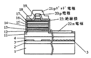
図1〜図3に基づき実施例1について説明する。図3は図1のレーザ素子にp電極を形成した後の構造を示す模式断面図であり、図1〜図3において同一符号で示されている箇所は同一箇所を示している。
【0025】
(下地層2)
2インチφ、C面を主面とするサファイアよりなる異種基板1をMOVPE反応容器内にセットし、温度を500℃にして、トリメチルガリウム(TMG)、アンモニア(NH3)を用い、GaNよりなるバッファ層(図示せず)を200オングストロームの膜厚で成長させる。バッファ層成長後、温度を1050℃にして、同じくGaNよりなる下地層2を4μmの膜厚で成長させる。この下地層2は保護膜を部分的に表面に形成して、次に窒化物半導体基板の選択成長を行うための下地層として作用する。下地層2はAl混晶比X値が0.5以下のAlXGa1-XN(0≦X≦0.5)を成長させることが望ましい。0.5を超えると、結晶欠陥というよりも結晶自体にクラックが入りやすくなってしまうため、結晶成長自体が困難になる傾向にある。また膜厚はバッファ層よりも厚い膜厚で成長させて、10μm以下の膜厚に調整することが望ましい。基板はサファイアの他、SiC、ZnO、スピネル、GaAs等、窒化物半導体を成長させるために知られている、窒化物半導体と異なる材料よりなる基板を用いることができる。
【0026】
(保護膜3)
下地層2成長後、ウェーハを反応容器から取り出し、この下地層2の表面に、ストライプ状のフォトマスクを形成し、CVD装置によりストライプ幅10μm、ストライプ間隔(窓部)2μmのSiO2よりなる保護膜3を1μmの膜厚で形成する。保護膜の形状としてはストライプ状、ドット状、碁盤目状等どのような形状でも良いが、窓部よりも保護膜の面積を大きくする方が、結晶欠陥の少ない第2の窒化物半導体層3が成長しやすい。保護膜の材料としては、例えば酸化ケイ素(SiOX)、窒化ケイ素(SiXNY)、酸化チタン(TiOX)、酸化ジルコニウム(ZrOX)等の酸化物、窒化物、またこれらの多層膜の他、1200℃以上の融点を有する金属等を用いることができる。これらの保護膜材料は、窒化物半導体の成長温度600℃〜1100℃の温度にも耐え、その表面に窒化物半導体が成長しないか、若しくは成長しにくい性質を有している。
【0027】
(窒化物半導体基板4)
保護膜3形成後、ウェーハを再度MOVPEの反応容器内にセットし、温度を1050℃にして、TMG、アンモニアを用い、アンドープGaNよりなるGaNよりなる窒化物半導体基板4を20μmの膜厚で成長させる。成長後の窒化物半導体基板4の表面は、保護膜のストライプ中央部と、窓部のストライプ中央部にはストライプ状の保護膜と平行に結晶欠陥が表出していたが、後にレーザ素子のリッジ形成時に、リッジストライプがこの結晶欠陥に係らないようにすることにより、活性層に結晶欠陥が転位せず、素子の信頼性が向上する。窒化物半導体基板4はハライド気相成長法(HVPE)を用いて成長させることができるが、このようにMOVPE法により成長させることもできる。窒化物半導体基板はIn、Alを含まないGaNを成長させることが最も好ましく、成長時のガスとしては、TMGの他、トリエチルガリウム(TEG)等の有機ガリウム化合物を用い、窒素源はアンモニア、若しくはヒドラジンを用いることが最も望ましい。また、このGaN基板にSi、Ge等のn型不純物をドープしてキャリア濃度を適当な範囲に調整してもよい。特に異種基板1、下地層2、保護膜3を除去する場合には、窒化物半導体基板がコンタクト層となるため、この窒化物半導体基板4にn型不純物をドープすることが望ましい。
【0028】
(n側バッファ層11=兼n側コンタクト層)
次に、アンモニアとTMG、不純物ガスとしてシランガスを用い、第2の窒化物半導体層4の上にSiを3×10¹⁸/cm3ドープしたGaNよりなるn側バッファ層11を5μmの膜厚で成長させる。このバッファ層は、図1のような構造の発光素子を作製した場合にはn電極を形成するためのコンタクト層として作用する。また異種基板1〜保護膜3を除去して、窒化物半導体基板4に電極を設ける場合には、省略することもできる。このn側バッファ層11は高温で成長させるバッファ層であり、例えばサファイア、SiC、スピネルのように窒化物半導体体と異なる材料よりなる基板の上に、900℃以下の低温において、GaN、AlN等を、0.5μm以下の膜厚で直接成長させるバッファ層とは区別される。
【0029】
(クラック防止層12)
次に、TMG、TMI(トリメチルインジウム)、アンモニアを用い、温度を800℃にしてIn0.06Ga0.94Nよりなるクラック防止層12を0.15μmの膜厚で成長させる。
【0030】
(n側クラッド層13=超格子層)
続いて、1050℃でTMA、TMG、アンモニア、シランガスを用い、Siを1×10¹⁹/cm3ドープしたn型Al0.16Ga0.84Nよりなる第1の層を25オングストロームの膜厚で成長させ、続いてシランガス、TMAを止め、アンドープのGaNよりなる第2の層を25オングストロームの膜厚で成長させる。そして第1層+第2層+第1層+第2層+・・・というように超格子層を構成し、総膜厚1.2μmの超格子よりなるn側クラッド層13を成長させる。この超格子よりなるn側クラッド層はAl平均組成が8.0%であるので、その膜厚との積は9.6となる。なおn側クラッド層に、バンドギャップエネルギーが異なる窒化物半導体を積層した超格子を作製した場合、不純物はいずれか一方の層に多くドープして、いわゆる変調ドープを行うと閾値が低下しやすい傾向にある。
【0031】
(n側光ガイド層14)
続いて、シランガスを止め、1050℃でアンドープGaNよりなるn側光ガイド層14を0.1μmの膜厚で成長させる。このn側光ガイド層は、活性層の光ガイド層として作用し、GaN、InGaNを成長させることが望ましく、通常100オングストローム〜5μm、さらに好ましくは200オングストローム〜1μmの膜厚で成長させることが望ましい。
【0032】
(活性層15)
次に、TMG、TMI、アンモニアを用い活性層14を成長させる。活性層は温度を800℃に保持して、アンドープIn0.2Ga0.8Nよりなる井戸層を40オングストロームの膜厚で成長させる。次にTMIのモル比を変化させるのみで同一温度で、アンドープIn0.01Ga0.95Nよりなる障壁層を100オングストロームの膜厚で成長させる。井戸層と障壁層とを順に積層し、最後に障壁層で終わり、総膜厚440オングストロームの多重量子井戸構造(MQW)の活性層を成長させる。活性層は本実施例のようにアンドープでもよいし、またn型不純物及び/又はp型不純物をドープしても良い。不純物は井戸層、障壁層両方にドープしても良く、いずれか一方にドープしてもよい。
【0033】
(p側キャップ層16)
次に、温度を1050℃に上げ、TMG、TMA、アンモニア、Cp2Mg(シクロペンタジエニルマグネシウム)を用い、p側光ガイド層17よりもバンドギャップエネルギーが大きい、Mgを1×10²⁰/cm3ドープしたp型Al0.3Ga0.7Nよりなるp側キャップ層16を300オングストロームの膜厚で成長させる。このp型キャップ層16は0.1μm以下の膜厚で形成することにより素子の出力が向上する傾向にある。膜厚の下限は特に限定しないが、10オングストローム以上の膜厚で形成することが望ましい。
【0034】
(p側光ガイド層17)
続いてCp2Mg、TMAを止め、1050℃で、バンドギャップエネルギーがp側キャップ層16よりも小さい、アンドープGaNよりなるp側光ガイド層17を0.1μmの膜厚で成長させる。この層は、活性層の光ガイド層として作用し、n型光ガイド層14と同じくGaN、InGaNで成長させることが望ましい。
【0035】
(p側クラッド層18)
続いて、1050℃でMgを1×10²⁰/cm3ドープしたp型Al0.16Ga0.84Nよりなる第3の層を25オングストロームの膜厚で成長させ、続いてTMAのみを止め、アンドープGaNよりなる第4の層を25オングストロームの膜厚で成長させ、総膜厚0.6μmの超格子層よりなるp側クラッド層18を成長させる。このp側クラッド層もAlの平均組成が8%であるので、膜厚との積は4.8となる。なお、p側クラッド層も少なくとも一方がAlを含む窒化物半導体層を含み、互いにバンドギャップエネルギーが異なる窒化物半導体層を積層した超格子で作製した場合、不純物はいずれか一方の層に多くドープして、いわゆる変調ドープを行うと閾値が低下しやすい傾向にある。
【0036】
ここで、クラッド層で挟まれたコア部分(導波部分)の膜厚について述べる。コア部分とは、n側光ガイド層14、活性層15、p側キャップ層16、及びp側光ガイド層17を合わせた領域、即ちn側クラッド層と、p側クラッド層との間にある活性層を含む窒化物半導体層を指し、活性層の発光を導波する領域である。窒化物半導体レーザ素子の場合、FFPが単一ビームとならないのは、先にも述べたように、クラッド層から漏れた発光がn側のコンタクト層内で導波してマルチモードになるからである。その他、コア内で共振することによってマルチモードになる場合がある。本発明ではまずn側のクラッド層の膜厚を厚くして、Al平均組成を大きくすることにより、屈折率差を設け、コア内の光をクラッド層で閉じ込めるものである。しかし、コア内でマルチモードができると、FFPは乱れる。そのため、本発明のn側クラッド層との関係において、コア内でマルチモードにならないようにするために、このコア部分の厚さも調整する方が望ましい。コア部分にマルチモードが発生しないようにするための好ましい厚さとしては、200オングストローム以上、1.0μm以下、さらに望ましくは500オングストローム〜0.8μm、最も望ましくは0.1μm〜0.5μmの範囲に調整することが望ましい。200オングストロームよりも薄いと、コア部分から光が漏れだし、閾値が上昇する傾向にある。また1.0μmよりも厚いとマルチモードになりやすい傾向にある。
【0037】
(p側コンタクト層19)
最後に、1050℃で、p側クラッド層18の上に、Mgを2×10²⁰/cm3ドープしたp型GaNよりなるp側コンタクト層18を150オングストロームの膜厚で成長させる。p側コンタクト層19はp型のInXAlYGa1-X-YN(0≦X、0≦Y、X+Y≦1)で構成することができ、好ましくはMgをドープしたGaNとすれば、p電極21と最も好ましいオーミック接触が得られる。
【0038】
以上のようにして窒化物半導体を成長させたウェーハを反応容器内において、窒素雰囲気中700℃でアニーリングを行い、p型不純物をドープした層をさらに低抵抗化させる。
【0039】
アニーリング後、ウェーハを反応容器から取り出し、RIE装置により最上層のp側コンタクト層18と、p側クラッド層17の一部とをエッチングして、図1、及び図2に示すような形状のリッジストライプを形成する。このリッジストライプは片方の共振面側のストライプ幅を2.0μmに設定し、もう片方の共振面側のストライプ幅を4.0μmに設定してあり、共振器長を500μmに設定することにより、レーザ共振方向に対する角度θを3゜以下にしている。なお、本実施例ではp側クラッド層の一部をリッジストライプとしているが、エッチング深さを深くして、p側クラッド層の全部をリッジストライプとすることもできる。
【0040】
また、リッジストライプを形成する際、そのリッジストライプは、窒化物半導体基板の表面に結晶欠陥が現れていない位置に形成する。結晶欠陥はストライプ状の保護膜3中央部、及びストライプ状の窓部中央部に現れやすい傾向にある。そのためその中央部を避けてリッジストライプを形成することにより、結晶欠陥が活性層まで伸びてこなくなる傾向にあるため、素子を長寿命とすることができ、信頼性が向上する。
【0041】
次にリッジ表面にマスクを形成し、RIEにてエッチングを行い、n側バッファ層11の表面を露出させる。露出させたこのn側バッファ層11はn電極23を形成するためのコンタクト層としても作用する。
【0042】
次にp側コンタクト層19のリッジ最表面にNiとAuよりなるp電極20をストライプ状に形成し、一方、TiとAlよりなるn電極22を先ほど露出させたn側バッファ層11の表面にストライプ状に形成した後、図3に示すようにp電極20と、n電極22との間に露出した窒化物半導体層の表面にSiO2よりなる絶縁膜23を形成し、この絶縁膜23を介してp電極20と電気的に接続したpパッド電極21を形成する。pパッド電極はp層側に漏れる光を吸収する。
【0043】
以上のようにして、n電極とp電極とを形成したウェーハのサファイア基板を研磨して70μmとした後、ストライプ状の電極に垂直な方向で、基板側からバー状に劈開し、劈開面に共振器を作製する。共振器面にSiO2とTiO2よりなる誘電体多層膜を形成し、最後にp電極に平行な方向で、バーを切断してレーザ素子とする。
【0044】
このレーザ素子をヒートシンクに設置し、それぞれの電極をワイヤーボンディングして、室温でレーザ発振を試みたところ、室温において連続発振を示し、単レーザ光のFFPは単一で、その形状も楕円形で形の良いものが得られていた。また、レーザ素子の特性に関しても、我々がJpn.J.Appl.Phys.Vol.36(1997)に発表したものに比較して、閾値が15%以上低下し、寿命は60%以上向上した。
【0045】
[実施例2]
実施例1において、n側クラッド層13を成長させる際に、Siドープn型Al0.20Ga0.80N25オングストロームと、アンドープGaN25オングストロとを積層し、総膜厚1.0μmの超格子よりなるn側クラッド層13を成長させる他は同様にしてレーザ素子を作製した。なおn側クラッド層はAl平均組成が10.0%であるので、その膜厚との積は10.0である。このレーザ素子も実施例1とほぼ同等の特性を有していた。
【0046】
[実施例3]
実施例1において、n側クラッド層13を成長させる際に、Siドープn型Al0.20Ga0.80N25オングストロームと、アンドープGaN25オングストロとを積層し、総膜厚0.7μmの超格子よりなるn側クラッド層13を成長させる他は同様にしてレーザ素子を作製した。n側クラッド層はAl平均組成が1.0%であるので、その膜厚との積は7.0である。このレーザ素子も実施例1とほぼ同等の特性を有していた。
【0047】
[実施例4]
実施例1において、n側クラッド層13を成長させる際に、Siドープn型Al0.12Ga0.88N25オングストロームと、アンドープGaN25オングストロとを積層し、総膜厚0.8μmの超格子よりなるn側クラッド層13を成長させる他は同様にしてレーザ素子を作製した。n側クラッド層はAl平均組成が6.0%であるので、その膜厚との積は4.8である。このレーザ素子もFFPは実施例1と同等であり、Jpn.J.Appl.Phys.Vol.36(1997)に発表したものに比較して、閾値が8%以上低下し、寿命は30%以上向上した。
【0048】
[実施例5]
実施例1において、n側クラッド層18を成長させる際に、Siドープn型Al0.07Ga0.93N層25オングストロームと、アンドープGaN層25オングストロームとを、総膜厚1.4μmで成長させる他は同様にして、レーザ素子を作製した。n側クラッド層は、Al平均組成が3.5%であるので、その膜厚との積は4.9である。このレーザ素子は実施例4のものとほぼ同等の特性を示した。
【0049】
[実施例6]
実施例1において、ストライプ状のリッジを形成する際、そのリッジ形状を図5に示すような形状とする。但し、図5において、両出力側のストライプ幅は2μmとし、中央部のストライプ幅は4μmとして、その傾斜角を5゜以内に調整する。このレーザ素子も実施例1とほぼ等々の特性を示した。
【0050】
【発明の効果】
以上説明したように、本発明によると水平横モード、垂直横モード共にシングルモードが得られる。しかもレーザ光伸すポット形状も単一な楕円となり、一定のFFPが得られる。窒化物半導体はサファイアという窒化物半導体よりも屈折率の小さい材料を使用するため、従来の問題は避けられないように思われてきたが、本発明によりサファイアに限らず、窒化物半導体よりも屈折率の小さい、どのような基板の上にレーザ素子を作製しても、シングルモードで、きれいな形状のレーザ光が得られるため、書き込み、読みとり光源として、その利用価値は非常に大きい。
【図面の簡単な説明】
【図1】 本発明の一実施例に係るレーザ素子の構造を示す斜視図。
【図2】 図1のレーザ素子をリッジ上部から見た平面図。
【図3】 図1のレーザ素子にp電極を形成した後の構造を示す模式断面図。
【図4】 リッジストライプの形状を示す平面図。
【図5】 本発明に係るレーザ素子のリッジストライプの一形状を示す平面図。
【図6】 本発明に係るレーザ素子のリッジストライプの一形状を示す平面図。
【図7】 本発明に係るレーザ素子のリッジストライプの一形状を示す平面図。
【図8】 従来のレーザ素子の構造を示す模式断面図。
【符号の説明】
1・・・異種基板
2・・・GaN下地層
3・・・保護膜
4・・・窒化物半導体基板
11・・・n側バッファ層
12・・・クラック防止層
13・・・n側クラッド層
14・・・n側光ガイド層
15・・・活性層
16・・・p側キャップ層
17・・・p側光ガイド層
18・・・p側クラッド層
19・・・p側コンタクト層
20・・・p電極
21・・・pパッド電極
22・・・n電極
23・・・絶縁膜[0001]
[Industrial application fields]
The present invention relates to a laser element made of a nitride semiconductor (InaAlbGa1-a-bN, 0 ≦ a, 0 ≦ b, a + b ≦ 1).
[0002]
[Prior art]
We have produced a nitride semiconductor laser device including an active layer on a nitride semiconductor substrate, and have achieved the world's first continuous oscillation at room temperature of 10,000 hours or more (ICNS'97 Proceedings, October 27-31, 1997, P444-446, and Jpn. J. Appl. Phys. Vol. 36 (1997) pp. L1568-1571,
[0003]
The basic laser device structure is a super-layer composed of n-Al0.14Ga0.86N / GaN, in which an active layer in which a barrier layer made of In0.02Ga0.98N and a well layer made of In0.15Ga0.85N are stacked. It has a double heterostructure sandwiched between an n-side cladding layer having a lattice structure and a p-side cladding layer having a superlattice structure made of p-Al0.14Ga0.86N / GaN. Each of the single nitride semiconductor layers constituting the superlattice has a thickness of 25 angstroms. Further, a ridge having the same stripe width is formed on a part of the p-type cladding layer. The light emitted from the active layer is concentrated in the waveguide region under the ridge stripe, resonates between the resonance surfaces, and is emitted as a laser.
[0004]
[Problems to be solved by the invention]
However, in the conventional laser element, the laser light tends to be multimode. The horizontal transverse mode is made single mode by narrowing the ridge stripe, but if the stripe width is narrowed to obtain the single mode, it tends to be difficult to form an ohmic electrode formed on the ridge stripe. . In addition, since the electrode area is reduced, the current concentrates in a minute portion, thereby increasing the threshold value of the laser element or reducing the reliability of the element itself due to heat generation.
[0005]
On the other hand, in the vertical transverse mode, light confinement by both cladding layers tends to be insufficient. For example, light leaked from the n-side cladding layer is reflected by a sapphire substrate having a low refractive index and guided in a GaN layer having a high refractive index between the substrate and the n-side cladding layer. The light guided in the GaN layer overlaps with the laser light emitted from the end face of the active layer and disturbs the shape of the far field pattern (FFP). Observed as a mode. A multimode laser element is very difficult to use as a light source for pickup.
[0006]
Therefore, an object of the present invention is to use a nitride semiconductor laser element as various light sources, so that it has single mode NFP and FFP, and oscillates laser light for a long time with a low threshold.
[0007]
[Means for Solving the Problems]
The nitride semiconductor laser device of the present invention isThis can be achieved by the following configurations (1) to (9).
(1) The substrate has an n-side cladding layer, an active layer, a p-side cladding layer, and a p-side contact layer in this order, and has a ridge above the active layer, with respect to the opposing resonant surface In the nitride semiconductor laser device in which the laser beam resonates substantially vertically, the p-side cladding layer is made of a superlattice having a nitride semiconductor layer containing at least Al, and is one of the p-side contact layer and the p-side cladding layer. The ridge is formed in a part or all of the ridge, the p-side contact layer has a striped p-electrode on the ridge outermost surface, and an insulating film is formed on the exposed surfaces of the p-side contact layer and the p-side cladding layer. A p-pad electrode electrically connected to the p-electrode through the insulating film, and the stripe width of the ridge becomes narrower as it approaches both resonance planes, and on the resonance plane of the laser element Lean Characterized in that it is formed to have a corner.
Furthermore, as a specific nitride semiconductor laser element of the present invention,
(2) When the total thickness of the p-side cladding layer is 50 mm or more and 2.0 μm or less and the Al average composition contained in the p-side cladding layer is expressed in percentage (%), the Al average composition (% ) Is 50% or less, and the product of the total thickness (μm) of the p-side cladding layer and the Al average composition (%) is preferably 4.4 or more.
(3) Preferably, the nitride semiconductor layer including the active layer between the n-side and p-side cladding layers has a thickness in the range of 200 angstroms to 1.0 μm.
(4) The thickness of the p-side cladding layer is preferably smaller than the thickness of the n-side cladding layer.
(5) The nitride semiconductor layer containing Al is made of Al. X Ga 1-X N (0 <X <1) is preferable.
(6) The inclination angle is preferably 10 ° or less.
(7) The substrate is preferably a nitride semiconductor substrate.
(8) It is preferable that an electrode is provided on the nitride semiconductor substrate.
(9) The nitride semiconductor laser element is preferably formed by cleaving the substrate.
[0008]
Furthermore, the ridge stripe is characterized in that the stripe width on the output side is narrower than the stripe width on the total reflection side. The laser output side and the total reflection side can be determined as appropriate by adjusting the reflectance of the reflective film formed on the resonance surface, for example.
[0009]
In the laser device of the present invention, the n-side cladding layer is made of a superlattice having a nitride semiconductor layer containing at least Al, and the entire thickness of the n-side cladding layer is 0.5 μm or more. When the average Al composition contained in the side cladding layer is expressed as a percentage (%), the product of the total thickness (μm) of the n-side cladding layer and the Al average composition (%) is 4.4 or more. It is configured.
[0010]
Further, when the thickness of the entire p-side cladding layer is 2.0 μm or less and the Al average composition contained in the p-side cladding layer is expressed as a percentage (%), the thickness of the entire p-side cladding layer The product of (μm) and Al average composition (%) is configured to be 4.4 or more.
[0011]
Furthermore, in the laser element of the present invention, the nitride semiconductor layer including the active layer between the n-side and p-side cladding layers has a thickness in the range of 200 angstroms to 1.0 μm. Features.
[0012]
DETAILED DESCRIPTION OF THE INVENTION
In the laser device of the present invention, the cladding layer is an optical confinement layer including a nitride semiconductor having a refractive index smaller than that of the well layer of the active layer. A superlattice refers to a multilayer structure in which nitride semiconductor layers having a single layer thickness of 100 angstroms or less and different compositions are laminated, preferably 70 angstroms or less, more preferably 40 angstroms or less. A physical semiconductor layer is stacked. As a specific configuration, for example, a superlattice in which an AlXGa1-XN (0 <X <1) layer and another nitride semiconductor layer having a composition different from that of the AlXGa1-XN layer is formed, for example, AlXGa1-XN / GaN. AlxGa1-XN / AlYGa1-YN (0 <Y <1, Y <X), AlXGa1-XN / InZGa1-ZN (0 <Z <1), etc. A superlattice can be formed by a combination of a crystal and a binary mixed crystal. Among them, the superlattice composed of AlxGa1-XN and GaN is most preferable. The same applies to the case where the n-side cladding layer is a superlattice. Needless to say, the cladding layer and the active layer need not be formed in contact with each other.
[0013]
FIG. 1 is a schematic perspective view showing the shape of the laser device of the present invention, and also shows a laminated structure. FIG. 2 is a plan view of the laser element of FIG. 1 viewed from the ridge side. This laser element is formed such that a ridge stripe is formed in a part of the p-
[0014]
In this way, preferably, the stripe width on the output side of the ridge is narrowed and the other total reflection side is widened, so that the laser beam under the ridge becomes a single mode in the horizontal transverse mode where the stripe width is narrow. On the other hand, where the stripe width is wide, there is a possibility that it becomes multimode below the ridge, but since it is already single in the narrow part, it is wide while the guided light is resonating between the resonance surfaces. Since the multimode is attenuated in a narrow portion, the laser beam emitted from the resonance surface corresponding to the portion having a wide stripe width is also changed to a single mode. In addition, since there are a portion where the stripe width of the ridge is gradually narrowed and a portion where the stripe width is gradually widened, the surface area is almost the same as that provided with stripe widths at equal intervals or substantially wide. Therefore, the current does not concentrate in a narrow region and flows evenly in the ridge, so that the heat generation of the element itself is reduced and the reliability is improved.
[0015]
FIG. 4 is a plan view showing the shape of the ridge. Unlike FIG. 2, the n-electrode is omitted. Referring to this figure, when the stripe ridge is formed, the stripe width a on the output side is desirably adjusted to a range of 0.5 μm to 5 μm, more preferably 1 μm to 2 μm. If it is narrower than 0.5 μm, the ridge width of the contact layer laminated on the clad layer is also narrowed, and it tends to be difficult to form an ohmic p-electrode. On the other hand, the stripe width b on the total reflection side is desirably adjusted to a range of 2 μm to 20 μm, more preferably 4 μm to 6 μm. If it is narrower than 2 μm, the other stripe width a must be narrower than 2 μm. For this reason, the entire ridge width becomes too narrow, and the current tends to be concentrated on the ridge, so that the device tends to generate heat. On the other hand, if the width is larger than 20 μm, the light loss at the lower portion of the ridge tends to be large and the output tends to decrease.
[0016]
Further, as shown in FIG. 4, it is most preferable that the stripe shape of the ridge does not have “necking” in the middle, and narrows to either one at a certain angle. In the present invention, it is desirable that the angle be as small as possible. For example, the angle θ with respect to the direction horizontal to the laser resonance direction is adjusted to within 10 °, more preferably within 8 °, and most preferably within 5 °. When the angle becomes steep, light leaks from the steep part to the outside, making it difficult for the light to concentrate at the bottom of the ridge, resulting in poor laser efficiency, low output, and high threshold. It is in. Therefore, in the present invention, it is desirable to form a ridge stripe that becomes gradually narrower as it approaches the end surface at an angle as gentle as possible, with the narrower side as the output side and the wider side as the total reflection side. As a preferable ridge stripe, it is most preferable to form a ridge stripe having an output side a of 1 to 3 μm, a total reflection side of 3 to 8 μm, and an inclination angle of 3 ° or less.
[0017]
5 to 7 are plan views showing other ridge stripe shapes according to the present invention. In the present invention, as shown in FIGS. 5 to 6, both ridge stripe widths may be formed so as to become narrower as they approach the resonance surface. Further, as shown in FIG. 7, the stripe may have a shape in which one side becomes narrower and the other side becomes wider as the resonance surface is approached. However, as shown in FIG. 5 to FIG. 7, when the stripe width is abruptly narrowed, the angle [theta] increases, and light tends to leak from the constricted portion, and the laser output tends to decrease. Therefore, when forming the ridge stripe as shown in FIGS. 5 to 7, it is desirable to adjust the inclination angle within 10 °.
[0018]
Furthermore, in the present invention, the n-side cladding layer is made of a superlattice having a nitride semiconductor layer containing at least Al, the entire thickness of the n-side cladding layer is 0.5 μm or more, and the n-side cladding layer includes By representing the Al average composition contained in percentage (%), the product of the total thickness (μm) of the n-side cladding layer and Al average composition (%) is 4.4 or more. The laser beam in the vertical and transverse modes can be controlled, and the single mode is easily obtained. When the thickness of the n-side cladding layer is less than 0.5 μm and the product of the total thickness (μm) of the n-side cladding layer and the Al average composition (%) is less than 4.4, the n-side cladding The light confinement as a layer becomes insufficient, the light is guided by the contact layer on the n side, FFP is disturbed, and the threshold value tends to increase. A preferable product value is 5.0 or more, more preferably 5.4 or more. Adjust to 7 or more as the best mode.
[0019]
For example, the total thickness of the n-side cladding layer is 0.8 μm or more, and the Al average composition contained in the n-side cladding layer is 5.5% or more. The product in this case is 4.4 or more. Preferably, the total thickness of the n-side cladding layer is 1.0 μm or more, and the Al average composition contained in the n-side cladding layer is 5.0% or more. The product in this case is 5.0 or more. More preferably, the total thickness of the n-side cladding layer is 1.2 μm or more, and the Al average composition contained in the n-side cladding layer is 4.5% or more. In this case, the product is 5.4 or more. This specifically shows the relationship between the thickness of the n-side cladding layer and the Al average composition of the n-side cladding layer made of a superlattice.
[0020]
In addition, regarding the p-side cladding layer, when the thickness of the entire p-side cladding layer is 2.0 μm or less and the Al average composition contained in the p-side cladding layer is expressed as a percentage (%), the p-side cladding layer The product of the total thickness (μm) and the Al average composition (%) may be 4.4 or more. With this configuration, the laser beam in the vertical and transverse modes can be controlled, and the single mode is easily obtained. In addition, it is more preferable that the n-side cladding layer has the above configuration than the p-side cladding layer. This is because the p-side cladding layer is formed as a ridge stripe having the shape as in the present application, and light is absorbed by the electrode, so even if there is leakage of light in the vertical transverse mode, it is almost ignored. Because it can.
[0021]
However, when the p-side cladding layer is configured as described above, it is desirable that the thickness of the p-side cladding layer be smaller than that of the n-side cladding layer. This is because when the Al average composition of the p-side cladding layer is increased or the film thickness is increased, the resistance value of the AlGaN layer tends to increase, and when the resistance value of AlGaN increases, the driving voltage tends to increase. Because. The preferred film thickness is 1.5 μm or less, more preferably 1 μm or less. The lower limit is not particularly limited, but in order to act as a cladding layer, it is desirable to have a film thickness of 50 angstroms or more, and the average composition of Al is desirably 50% or less.
[0022]
In general, it is known that AlxGa1-XN has a larger band gap energy and a smaller refractive index as the Al mixed crystal ratio is increased. Ideally, it would be industrially convenient if an AlXGa1-XN layer having a large Al mixed crystal ratio X, for example 0.5 or more, can be grown as a single layer with a film thickness of, for example, several μm. AlXGa1-XN is difficult to grow with a thick film. If AlxGa1-XN having an Al mixed crystal ratio of 0.5 or more is to be grown in a single layer, cracks will occur in the crystal at, for example, 0.1 μm or more. However, if Al x Ga 1-XN is a thin film constituting a superlattice as in the present invention, the single film thickness is less than the critical limit film thickness of Al x Ga 1-XN, so that cracks are unlikely to occur. Therefore, if the cladding layer is a superlattice, even a layer having a high Al mixed crystal ratio can be grown with a thick film, and by combining them, light can be prevented from leaking from the n-side cladding layer to the substrate side. .
[0023]
In the present invention, the Al average composition in the superlattice is obtained by the following calculation method. For example, in the case of a superlattice obtained by laminating 200 pairs (1.0 μm) of 25 Å Al0.5Ga0.5N and 25 Å GaN, one pair is 50 Å, and the Al mixed crystal ratio of the Al-containing layer is 0. Therefore, 0.5 (25/50) = 0.25, and the Al average composition in the superlattice is 25%. On the other hand, when the film thickness is different, when Al0.5Ga0.5N is laminated at 40 angstroms and GaN is laminated at 20 angstroms, the weighted average of the film thickness is obtained, and 0.5 (40/60) = 0.33. The Al average composition is 33.3%. That is, the Al average composition of the superlattice in the present invention is obtained by multiplying the Al mixed crystal ratio of the nitride semiconductor layer containing Al by the ratio of the nitride semiconductor layer to the film thickness of one pair of superlattices. The same applies to the case where both Al are contained. For example, 0.1 (20/50) +0.2 (30/50) = 0.16 in the case of Al0.1Ga0.9N20 angstrom and Al0.2Ga0.8N30 angstrom. In other words, 16% is Al average composition. In the above example, AlGaN / GaN and AlGaN / AlGaN have been described. However, the same calculation method is applied to AlGaN / InGaN. Therefore, when growing the n-side cladding layer, the growth method can be designed based on the above calculation method. Further, the Al average composition of the n-side cladding layer can be detected using an analyzer such as SIMS (secondary ion mass spectrometer) or Auger.
[0024]
【Example】
[Example 1]
A first embodiment will be described with reference to FIGS. FIG. 3 is a schematic cross-sectional view showing the structure after the p-electrode is formed on the laser element of FIG. 1, and the portions denoted by the same reference numerals in FIGS. 1 to 3 indicate the same portions.
[0025]
(Underlayer 2)
A
[0026]
(Protective film 3)
After the
[0027]
(Nitride semiconductor substrate 4)
After the
[0028]
(N-
Next, an n-
[0029]
(Crack prevention layer 12)
Next, the
[0030]
(N-
Subsequently, using TMA, TMG, ammonia, and silane gas at 1050 ° C., a first layer made of n-type Al0.16Ga0.84N doped with 1 × 10 19 /
[0031]
(N-side light guide layer 14)
Subsequently, the silane gas is stopped, and an n-side
[0032]
(Active layer 15)
Next, the
[0033]
(P-side cap layer 16)
Next, the temperature was raised to 1050 ° C., TMG, TMA, ammonia,
[0034]
(P-side light guide layer 17)
Subsequently, Cp2Mg and TMA are stopped, and a p-side
[0035]
(P-side cladding layer 18)
Subsequently, a third layer made of p-type Al0.16Ga0.84N doped with 1 × 10²⁰ / cm3 Mg at 1050 ° C. is grown to a thickness of 25 Å, and then only TMA is stopped, and a third layer made of undoped GaN is grown. 4 is grown to a thickness of 25 Å, and a p-
[0036]
Here, the film thickness of the core portion (waveguide portion) sandwiched between the clad layers will be described. The core portion is a region where the n-side
[0037]
(P-side contact layer 19)
Finally, a p-
[0038]
The wafer on which the nitride semiconductor is grown as described above is annealed in a reaction vessel at 700 ° C. in a nitrogen atmosphere to further reduce the resistance of the layer doped with the p-type impurity.
[0039]
After annealing, the wafer is removed from the reaction vessel, and the uppermost p-
[0040]
Further, when forming the ridge stripe, the ridge stripe is formed at a position where no crystal defect appears on the surface of the nitride semiconductor substrate. Crystal defects tend to appear at the center of the stripe-shaped
[0041]
Next, a mask is formed on the ridge surface and etching is performed by RIE to expose the surface of the n-
[0042]
Next, a p-electrode 20 made of Ni and Au is formed in a stripe shape on the ridge outermost surface of the p-
[0043]
As described above, after polishing the sapphire substrate of the wafer on which the n-electrode and the p-electrode are formed to 70 μm, the substrate is cleaved in a bar shape from the substrate side in a direction perpendicular to the stripe-shaped electrode, A resonator is manufactured. A dielectric multilayer film made of SiO2 and TiO2 is formed on the resonator surface, and finally a bar is cut in a direction parallel to the p-electrode to form a laser element.
[0044]
When this laser element was placed on a heat sink and each electrode was wire-bonded and laser oscillation was attempted at room temperature, it showed continuous oscillation at room temperature. The single laser beam had a single FFP and its shape was elliptical. A good shape was obtained. As for the characteristics of the laser element, the threshold value was reduced by 15% or more and the lifetime was improved by 60% or more compared to what we published in Jpn.J.Appl.Phys.Vol.36 (1997).
[0045]
[Example 2]
In Example 1, when the n-
[0046]
[Example 3]
In Example 1, when the n-
[0047]
[Example 4]
In Example 1, when the n-
[0048]
[Example 5]
In Example 1, when the n-
[0049]
[Example 6]
In Example 1, when forming a striped ridge, the ridge shape is as shown in FIG. However, in FIG. 5, the stripe width on both output sides is 2 μm, the stripe width at the center is 4 μm, and the inclination angle is adjusted within 5 °. This laser device also exhibited almost the same characteristics as Example 1.
[0050]
【The invention's effect】
As described above, according to the present invention, a single mode can be obtained in both the horizontal and vertical modes. Moreover, the pot shape for laser beam extension is also a single ellipse, and a constant FFP is obtained. Nitride semiconductors use a material called sapphire, which has a lower refractive index than nitride semiconductors, so it seems that conventional problems cannot be avoided. Even if a laser element is manufactured on any substrate having a low rate, a laser beam having a clean shape can be obtained in a single mode.
[Brief description of the drawings]
FIG. 1 is a perspective view showing a structure of a laser device according to an embodiment of the present invention.
FIG. 2 is a plan view of the laser device of FIG. 1 as viewed from above the ridge.
3 is a schematic cross-sectional view showing a structure after a p-electrode is formed on the laser element of FIG.
FIG. 4 is a plan view showing the shape of a ridge stripe.
FIG. 5 is a plan view showing one shape of a ridge stripe of the laser element according to the present invention.
FIG. 6 is a plan view showing one shape of a ridge stripe of the laser element according to the present invention.
FIG. 7 is a plan view showing one shape of a ridge stripe of the laser device according to the present invention.
FIG. 8 is a schematic cross-sectional view showing the structure of a conventional laser element.
[Explanation of symbols]
1 ... Different substrates
2 ... GaN underlayer
3 ... Protective film
4 ... Nitride semiconductor substrate
11 ... n-side buffer layer
12 ... Crack prevention layer
13 ... n-side cladding layer
14 ... n-side light guide layer
15 ... Active layer
16 ... p-side cap layer
17 ... p-side light guide layer
18 ... p-side cladding layer
19 ... p-side contact layer
20 ... p electrode
21 ... P pad electrode
22 ... n electrode
23 ... Insulating film
Claims (9)
活性層よりも上の層にリッジを有し、対向する共振面に対してほぼ垂直にレーザ光が共振する窒化物半導体レーザ素子において、
前記p側クラッド層は、少なくともAlを含む窒化物半導体層を有する超格子よりなり、
前記p側コンタクト層とp側クラッド層の一部、若しくは全部に前記リッジが形成されており、
前記p側コンタクト層のリッジ最表面にストライプ状のp電極を有し、露出した前記p側コンタクト層とp側クラッド層の表面に絶縁膜を有し、該絶縁膜を介して前記p電極と電気的に接続したpパッド電極を有し、
さらに該リッジのストライプ幅が両方の共振面に接近するに従って狭くなり、かつレーザ素子の共振面において傾斜角を有するように形成されていることを特徴とする窒化物半導体レーザ素子。An n-side cladding layer, an active layer, a p-side cladding layer, and a p-side contact layer in that order on the substrate;
In a nitride semiconductor laser device having a ridge in the layer above the active layer and in which the laser beam resonates substantially perpendicularly to the opposing resonance surface,
The p-side cladding layer is made of a superlattice having a nitride semiconductor layer containing at least Al,
The ridge is formed in part or all of the p-side contact layer and the p-side cladding layer,
The p-side contact layer has a striped p-electrode on the ridge outermost surface, an exposed insulating layer on the exposed p-side contact layer and the p-side cladding layer, and the p-electrode through the insulating film An electrically connected p-pad electrode;
Further nitride semiconductor laser device characterized by being formed so that the have a tilt angle in a narrow of Ri, and the resonance surface of the laser element according to the stripe width of the ridge is close to both of the resonance surface.
Priority Applications (1)
| Application Number | Priority Date | Filing Date | Title |
|---|---|---|---|
| JP2002354976A JP3891108B2 (en) | 2002-12-06 | 2002-12-06 | Nitride semiconductor light emitting device |
Applications Claiming Priority (1)
| Application Number | Priority Date | Filing Date | Title |
|---|---|---|---|
| JP2002354976A JP3891108B2 (en) | 2002-12-06 | 2002-12-06 | Nitride semiconductor light emitting device |
Related Parent Applications (1)
| Application Number | Title | Priority Date | Filing Date |
|---|---|---|---|
| JP35254097A Division JP3647236B2 (en) | 1997-12-22 | 1997-12-22 | Nitride semiconductor laser device |
Publications (3)
| Publication Number | Publication Date |
|---|---|
| JP2003163415A JP2003163415A (en) | 2003-06-06 |
| JP2003163415A5 JP2003163415A5 (en) | 2005-06-30 |
| JP3891108B2 true JP3891108B2 (en) | 2007-03-14 |
Family
ID=19197914
Family Applications (1)
| Application Number | Title | Priority Date | Filing Date |
|---|---|---|---|
| JP2002354976A Expired - Fee Related JP3891108B2 (en) | 2002-12-06 | 2002-12-06 | Nitride semiconductor light emitting device |
Country Status (1)
| Country | Link |
|---|---|
| JP (1) | JP3891108B2 (en) |
Families Citing this family (4)
| Publication number | Priority date | Publication date | Assignee | Title |
|---|---|---|---|---|
| JP2007305635A (en) * | 2006-05-09 | 2007-11-22 | Sharp Corp | Nitride semiconductor light-emitting element |
| JP2011082245A (en) * | 2009-10-05 | 2011-04-21 | Qd Laser Inc | Optical semiconductor device and optical module using the same |
| DE102011100175B4 (en) | 2011-05-02 | 2021-12-23 | OSRAM Opto Semiconductors Gesellschaft mit beschränkter Haftung | Laser light source with a ridge waveguide structure and a mode filter structure |
| DE102015119226A1 (en) | 2015-11-09 | 2017-05-11 | Osram Opto Semiconductors Gmbh | Semiconductor laser diode |
-
2002
- 2002-12-06 JP JP2002354976A patent/JP3891108B2/en not_active Expired - Fee Related
Also Published As
| Publication number | Publication date |
|---|---|
| JP2003163415A (en) | 2003-06-06 |
Similar Documents
| Publication | Publication Date | Title |
|---|---|---|
| JP4830315B2 (en) | Semiconductor laser element | |
| CA2449047C (en) | Semiconductor laser element with shading layers and improved far field pattern | |
| JP3647236B2 (en) | Nitride semiconductor laser device | |
| JP4304750B2 (en) | Nitride semiconductor growth method and nitride semiconductor device | |
| JPWO2003036771A1 (en) | Nitride semiconductor laser device and manufacturing method thereof | |
| US7609737B2 (en) | Nitride semiconductor laser element | |
| JP4665394B2 (en) | Nitride semiconductor laser device | |
| JP4291960B2 (en) | Nitride semiconductor device | |
| JP2004327637A (en) | Semiconductor laser element | |
| JP4991025B2 (en) | Nitride semiconductor laser device | |
| JP3794530B2 (en) | Nitride semiconductor laser device | |
| JP3888080B2 (en) | Semiconductor laser element | |
| JP4457417B2 (en) | Nitride semiconductor laser device | |
| JP3891108B2 (en) | Nitride semiconductor light emitting device | |
| JPH11238945A (en) | Nitride semiconductor light-emitting device | |
| JP3685682B2 (en) | Nitride semiconductor laser device | |
| JP3925066B2 (en) | Nitride semiconductor laser device | |
| JP4045792B2 (en) | Nitride semiconductor laser device | |
| JP5010096B2 (en) | Nitride semiconductor laser device and LD device using the same | |
| JP4955195B2 (en) | Nitride semiconductor device | |
| JP4576795B2 (en) | Nitride semiconductor laser device and manufacturing method thereof | |
| JP3656454B2 (en) | Nitride semiconductor laser device | |
| JP2002270967A (en) | Semiconductor laser element | |
| JP4032836B2 (en) | Nitride semiconductor laser device | |
| JP4815734B2 (en) | Nitride semiconductor laser device |
Legal Events
| Date | Code | Title | Description |
|---|---|---|---|
| A521 | Written amendment |
Free format text: JAPANESE INTERMEDIATE CODE: A523 Effective date: 20041021 |
|
| A621 | Written request for application examination |
Free format text: JAPANESE INTERMEDIATE CODE: A621 Effective date: 20041021 |
|
| A131 | Notification of reasons for refusal |
Free format text: JAPANESE INTERMEDIATE CODE: A131 Effective date: 20060627 |
|
| A521 | Written amendment |
Free format text: JAPANESE INTERMEDIATE CODE: A523 Effective date: 20060828 |
|
| TRDD | Decision of grant or rejection written | ||
| A01 | Written decision to grant a patent or to grant a registration (utility model) |
Free format text: JAPANESE INTERMEDIATE CODE: A01 Effective date: 20061114 |
|
| A61 | First payment of annual fees (during grant procedure) |
Free format text: JAPANESE INTERMEDIATE CODE: A61 Effective date: 20061127 |
|
| R150 | Certificate of patent or registration of utility model |
Free format text: JAPANESE INTERMEDIATE CODE: R150 |
|
| FPAY | Renewal fee payment (event date is renewal date of database) |
Free format text: PAYMENT UNTIL: 20091215 Year of fee payment: 3 |
|
| FPAY | Renewal fee payment (event date is renewal date of database) |
Free format text: PAYMENT UNTIL: 20091215 Year of fee payment: 3 |
|
| FPAY | Renewal fee payment (event date is renewal date of database) |
Free format text: PAYMENT UNTIL: 20101215 Year of fee payment: 4 |
|
| FPAY | Renewal fee payment (event date is renewal date of database) |
Free format text: PAYMENT UNTIL: 20101215 Year of fee payment: 4 |
|
| FPAY | Renewal fee payment (event date is renewal date of database) |
Free format text: PAYMENT UNTIL: 20111215 Year of fee payment: 5 |
|
| FPAY | Renewal fee payment (event date is renewal date of database) |
Free format text: PAYMENT UNTIL: 20111215 Year of fee payment: 5 |
|
| FPAY | Renewal fee payment (event date is renewal date of database) |
Free format text: PAYMENT UNTIL: 20121215 Year of fee payment: 6 |
|
| FPAY | Renewal fee payment (event date is renewal date of database) |
Free format text: PAYMENT UNTIL: 20121215 Year of fee payment: 6 |
|
| FPAY | Renewal fee payment (event date is renewal date of database) |
Free format text: PAYMENT UNTIL: 20131215 Year of fee payment: 7 |
|
| R250 | Receipt of annual fees |
Free format text: JAPANESE INTERMEDIATE CODE: R250 |
|
| R250 | Receipt of annual fees |
Free format text: JAPANESE INTERMEDIATE CODE: R250 |
|
| LAPS | Cancellation because of no payment of annual fees |