JP4032836B2 - Nitride semiconductor laser device - Google Patents
Nitride semiconductor laser device Download PDFInfo
- Publication number
- JP4032836B2 JP4032836B2 JP2002170643A JP2002170643A JP4032836B2 JP 4032836 B2 JP4032836 B2 JP 4032836B2 JP 2002170643 A JP2002170643 A JP 2002170643A JP 2002170643 A JP2002170643 A JP 2002170643A JP 4032836 B2 JP4032836 B2 JP 4032836B2
- Authority
- JP
- Japan
- Prior art keywords
- nitride semiconductor
- layer
- type
- substrate
- grown
- Prior art date
- Legal status (The legal status is an assumption and is not a legal conclusion. Google has not performed a legal analysis and makes no representation as to the accuracy of the status listed.)
- Expired - Lifetime
Links
Images


Description
【0001】
【発明の属する技術分野】
本発明は窒化物半導体(InXAlYGa1-X-YN(0≦X、0≦Y、X+Y≦1)よりなるレーザ素子とそのレーザ素子の共振面の作製方法に関する。
【0002】
【従来の技術】
紫外〜青色の領域に発光するレーザ素子の材料として窒化物半導体が知られており、本出願人は、最近この材料を用いてパルス電流において、室温でのレーザ発振を発表した(例えば、Jpn.J.Appl.Phys. Vol35 (1996) pp.L74-76)。発表したレーザ素子はいわゆる電極ストライプ型のレーザ素子であり、レーザの共振面はエッチングにより形成されている。エッチングで共振面を作製する方法は、簡単に共振面ができるという利点があるが、エッチング手段によりエッチングされた面に凹凸が発生しやすく、互いに平行な面が得られにくいという欠点がある。レーザの共振面は赤外、赤色半導体レーザで多用されているように、劈開して形成することが最も望ましい。例えばGaAs基板を用いた赤外半導体レーザであれば、その共振面は基板の劈開性が利用された劈開面が利用される。
【0003】
窒化物半導体はサファイア基板の上に成長されることが多く、サファイアは六方晶系(正確には菱面体であるが、六方晶系で近似される。)であるため劈開性がほとんどない。このためサファイア基板の上に成長された窒化物半導体層を、基板の劈開性を用いて劈開することは非常に困難であった。
【0004】
【発明が解決しようとする課題】
半導体レーザの共振面は凹凸が非常に少ない、いわば鏡面に近い平坦面にする必要がある。従って、本発明の目的とするところは、劈開により鏡面に近い共振面が得られた窒化物半導体レーザ素子と、そのレーザ素子の共振面の作製方法を提供することにある。
【0005】
【課題を解決するための手段】
従来、サファイアの上に成長されていた窒化物半導体は、サファイアが劈開性がないため、同様に六方晶系である窒化物半導体層も劈開性がないと信じられていたが、本発明者らは、基板に関わらず、特定の面方位で窒化物半導体層を割れば窒化物半導体層に劈開性があることを新規に見出し、本発明を成すに至った。即ち、本発明の窒化物半導体レーザ素子は、窒化物半導体の[外1]、[外2]、[外3]、[外4]、[外5]、[外6]の内のいずれか一種類の面方位に沿った劈開面が少なくとも一方の共振面とされている窒化物半導体レーザ素子において、GaN基板上に、n型窒化物半導体、量子井戸構造の活性層、p型窒化物半導体を有し、前記n型窒化物半導体は、前記GaN基板に接してSiを含有するIn x Al y Ga 1−x−y N(0≦x、0≦y、x+y≦1)層と、前記活性層に接するIn x Ga 1−x N(0≦x<1)層と、を有しており、前記p型窒化物半導体の上には正電極を有しており、前記GaN基板の裏面には負電極を有することを特徴とする。前記活性層は、InGaNまたはGaNを有する。
【0006】
また本発明のレーザ素子の共振面は、基板の上に複数の窒化物半導体層を成長させた後、最上層の窒化物半導体の【外1】乃至【外6】面の内のいずれか一種類に相当する面に溝を設け、その溝より窒化物半導体を劈開し、劈開された窒化物半導体層の劈開面をレーザ素子の少なくとも一方の共振面とする方法により作製できる。
【0007】
さらに本発明のレーザ素子は、窒化物半導体を成長させる基板が窒化物半導体単結晶である場合、その窒化物半導体単結晶よりなる基板の上に、複数の窒化物半導体層を成長させた後、窒化物半導体層を成長させた面と対向する基板の【外1】乃至【外6】面の内のいずれか一種類に相当する面に溝を設け、その溝より窒化物半導体を劈開し、劈開された窒化物半導体層の劈開面をレーザ素子の少なくとも一方の共振面とする方法により作製できる。
【0008】
【作用】
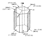
図1に窒化物半導体単結晶の面方位を示すユニットセル図を示す。窒化物半導体は正確には菱面体構造を有しているが、この図に示すように六方晶系で近似できる。本発明のレーザ素子はこのユニットセル図に示す【外1】〜【外6】の内のいずれか一種類の面方位に沿った劈開面が少なくとも一方の共振面とされている。この面方位は六角柱で示す側面に相当し、これらの面で劈開された窒化物半導体層面は鏡面に近い面が得られる。例えばこの図で示す斜線部は【外3】面と【外6】面とを示しており、このように対向する共振面を劈開で形成することが最も好ましいが、必ずしも両方とも劈開で形成する必要はなく、片方を劈開により形成して、もう片方を他の手段、例えばエッチングで形成しても良い。
【0009】
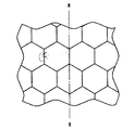
図2は、基板の上に成長された窒化物半導体の結晶構造を拡大して示す模式的な平面図である。窒化物半導体はこのように六角柱の単位結晶が集まった亀甲状に成長される。本発明の共振面の作製方法では、最上層の窒化物半導体の【外1】〜【外6】面の内のいずれか一種類に相当する面、例えばこの図に示すII−IIの延長線上にある窒化物半導体層の表面に溝を設け、その溝よりII−IIに示す線で窒化物半導体を劈開し、劈開された窒化物半導体層の劈開面をレーザ素子の共振面とすると、鏡面に近い共振面が得られる。溝とは言い換えると劈開するための傷であり、例えばダイヤモンドを刃先に有する罫書針で形成できる他、エッチングにより形成することもできる。なお、レーザ素子を作製する場合、最上層の窒化物半導体層には、通常、電極層が形成されるが、電極層を貫通して最上層の窒化物半導体層に劈開のための溝を設けることも、本発明の範囲内である。
【0010】
さらに、基板が窒化物半導体単結晶である場合は、基板そのものの劈開性が利用できるため、基板の上に成長させた窒化物半導体層側に傷を設ける必要はなく、窒化物半導体層を成長させた基板と反対側の面にある【外1】〜【外6】面の内のいずれか一種類に相当する面に傷を付けて、その傷から劈開すればよい。
【0011】
【発明の実施の形態】
本発明のレーザ素子の構造は劈開面を共振面とするレーザ素子であればどのようなものでも良く、素子構造は限定されない。例えば利得導波型ストライプ型レーザとして、電極ストライプ型、メサストライプ型、ヘテロアイソレーション型等を挙げることができる。またその他、作りつけ導波機構をもつストライプ型レーザとして、埋め込みヘテロ型、CSP型、リブガイド型等を挙げることができる。これらの構造のレーザ素子は、活性層中に導波路が作製され、導波路端面に相当する位置に共振面が作製されて、その共振面同士で活性層の発光が共振されて、導波路に沿って発振する。また、共振面に光の閉じ込めを図るために、通常行われているような誘電体多層膜を形成してもよい。
【0012】
[実施例1]
図3は本発明の一態様に係るレーザ素子の構造を示す模式的な断面図であり、共振面と平行な方向で切断した際の図を示している。以下、この図を元に実施例1について説明する。
【0013】
C軸配向した厚さ500μmのGaNよりなる基板10をMOVPE装置の反応容器内に設置した後、原料ガスにTMG(トリメチルガリウム)と、アンモニア、ドナー不純物としてSiH4(シラン)ガスを用いて、SiドープGaNよりなるn型コンタクト層11を4μmの膜厚で成長させた。
【0014】
本発明のレーザ素子では基板は特に限定されるものではなく、窒化物半導体を成長させるために、従来使用され、また提案されている全ての基板について適用可能である。例えば、GaNの他に、サファイア、スピネル、酸化亜鉛等の酸化物基板、Si、SiC等の半導体基板等が知られており、本発明ではいずれにも適用可能である。特に好ましくは、GaN、AlGaN等の窒化物半導体よりなる単結晶の基板を用いる。その理由は、前記したように窒化物半導体単結晶の基板を用いることにより、基板の劈開性を用いて共振面を形成することができるので、半導体層側に溝を設けずに、基板側に溝を設けて、その溝から【外1】〜【外6】面に従って劈開することができるからである。また基板が窒化物半導体と格子整合しているため、非常に膜質のよい結晶を成長できる。
【0015】
n型コンタクト層11はInXAlYGa1-X-YN(0≦X、0≦Y、X+Y≦1)で構成することができ、特にGaN、InGaN、その中でもSiをドープしたGaNで構成することにより、キャリア濃度の高いn型層が得られ、また負電極と好ましいオーミック接触が得られるので、レーザ素子のしきい値電流を低下させることができる。
【0016】
温度を1050℃に保持して、原料ガスにTMG、アンモニア、不純物ガスにCp2Mgを用い、Mgドープp型GaNよりなる電流阻止層20を0.5μmの膜厚で成長させた。この電流阻止層は後に、活性層に電流を集中させて導波路を作製する作用がある。
【0017】
電流阻止層20を成長後、ウェーハを反応容器から取り出し、電流阻止層20を図3に示すように、n型コンタクト層11に達する深さでV溝状にメサエッチした。V溝の幅は5μmとして、電流阻止層20の表面にストライプ状に深さ2.5μmで形成した。V溝状のストライプは、その溝の中にn型光閉じ込め層12、n型光ガイド層13、活性層14、p型光ガイド層15、及びp型光閉じ込め層16がV溝中に入りやすくなる。活性層から発するレーザ光は、縦方向が活性層の上下にある光閉じ込め層により制御される。V溝を形成すると、活性層15を挟む横方向の光閉じ込め層が溝中に入り込むことにより、レーザ光の横方向が制御でき、溝中に光閉じ込めが可能となるのでレーザのしきい値電流を下げることができる。つまり、V溝により横方向の活性層が屈折率の異なるクラッド層で挟まれたいわば屈折率導波のレーザ素子ができる。さらにV溝はメサ形状を有しているため、V溝の上に成長させる窒化物半導体層が均一な膜厚で結晶成長可能となる。
【0018】
次に、再度ウェーハを反応容器に移送し、温度を750℃にして、原料ガスにTMG、TMI(トリメチルインジウム)、アンモニア、不純物ガスにシランガスを用い、SiドープIn0.1Ga0.9Nよりなるクラック防止層を300オングストロームの膜厚で成長させた。このクラック防止層は特に図示していないが、Inを含むn型の窒化物半導体、好ましくはInGaNで成長させることにより、次に成長させるAlを含む窒化物半導体よりなるn型光閉じこめ層12を厚膜で成長させることが可能となる。LDの場合は、光閉じ込め層、光ガイド層となる層を、例えば0.1μm以上の膜厚で成長させる必要がある。従来ではGaN、AlGaN層の上に直接厚膜のAlGaNを成長させると、後から成長させたAlGaNにクラックが入るので素子作製が困難であったが、このクラック防止層が次に成長させる光閉じこめ層にクラックが入るのを防止することができる。しかも次に成長させる光閉じこめ層3を厚膜で成長させても膜質良く成長できる。なおこのクラック防止層は100オングストローム以上、0.5μm以下の膜厚で成長させることが好ましい。100オングストロームよりも薄いと前記のようにクラック防止として作用しにくく、0.5μmよりも厚いと、結晶自体が黒変する傾向にある。なお、このクラック防止層は成長方法、成長装置によっては省略することもできる。
【0019】
次に、原料ガスにTEG、TMA(トリメチルアルミニウム)、アンモニア、不純物ガスにシランガスを用いて、Siドープn型Al0.3Ga0.7Nよりなるn型光閉じこめ層12を0.5μmの膜厚で成長させた。n型光閉じこめ層12はAlを含むn型の窒化物半導体で構成し、好ましくは二元混晶あるいは三元混晶のAlYGa1-YN(0<Y≦1)とすることにより、結晶性の良いものが得られ、また活性層との屈折率差を大きくしてレーザ光の縦方向の閉じ込めに有効である。この層は通常0.1μm〜1μmの膜厚で成長させることが望ましい。0.1μmよりも薄いと光閉じ込め層として作用しにくく、1μmよりも厚いと、結晶中にクラックが入りやすくなり素子作成が困難となる傾向にある。
【0020】
続いて、原料ガスにTMG、アンモニア、不純物ガスにシランガスを用い、Siドープn型GaNよりなるn型光ガイド層13を500オングストロームの膜厚で成長させた。n型光ガイド層13は、Inを含むn型の窒化物半導体若しくはn型GaNで構成し、好ましくは三元混晶若しくは二元混晶のInXGa1-XN(0≦X<1)とする。この層は通常100オングストローム〜1μmの膜厚で成長させることが望ましく、特にInGaN、GaNとすることにより次の活性層を量子井戸構造とすることが容易に可能になる。
【0021】
次に原料ガスにTMG、TMI、アンモニアを用いて活性層14を成長させた。活性層は温度を750℃に保持して、まずノンドープIn0.2Ga0.8Nよりなる井戸層を25オングストロームの膜厚で成長させる。次にTMIのモル比を変化させるのみで同一温度で、ノンドープIn0.01Ga0.95Nよりなる障壁層を50オングストロームの膜厚で成長させる。この操作を13回繰り返し、最後に井戸層を成長させ総膜厚0.1μmの膜厚の多重量子井戸構造よりなる活性層14を成長させた。
【0022】
活性層14成長後、温度を1050℃にしてTMG、TMA、アンモニア、アクセプター不純物源としてCp2Mg(シクロペンタジエニルマグネシウム)を用い、Mgドープp型Al0.2Ga0.8Nよりなるp型キャップ層を100オングストロームの膜厚で成長させた。このp型キャップ層も特に図示していないが、AlYGa1-YN(0<Y<1)で形成することが好ましく、1μm以下、さらに好ましくは10オングストローム以上、0.1μm以下の膜厚で成長させることにより、InGaNよりなる活性層が分解するのを防止するキャップ層としての作用があり、また活性層の上にAlを含むp型窒化物半導体よりなるp型キャップ層を成長させることにより、発光出力が格段に向上する。逆に活性層に接するp層をGaNとすると素子の出力が約1/3に低下してしまう。これはAlGaNがGaNに比べてp型になりやすく、またp型キャップ層成長時に、InGaNが分解するのを抑える作用があるためと推察されるが、詳しいことは不明である。このp型キャップ層の膜厚は1μmよりも厚いと、層自体にクラックが入りやすくなり素子作製が困難となる傾向にある。なおこのp型キャップ層も省略可能である。
【0023】
次に温度を1050℃に保持しながら、TMG、アンモニア、Cp2Mgを用いMgドープp型GaNよりなるp型光ガイド層15を500オングストロームの膜厚で成長させた。このp型光ガイド層15は、Inを含む窒化物半導体若しくはGaNで構成し、好ましくは二元混晶または三元混晶のInYGa1-YN(0<Y≦1)を成長させる。光ガイド層は、通常100オングストローム〜1μmの膜厚で成長させることが望ましく、特にInGaN、GaNとすることにより、次のp型光閉じこめ層16を結晶性良く成長できる。
【0024】
続いて、TMG、TMA、アンモニア、Cp2Mgを用いてMgドープAl0.3Ga0.7Nよりなるp型光閉じこめ層16を0.5μmの膜厚で成長させた。このp型光閉じ込め層16は、Alを含むp型の窒化物半導体で構成し、好ましくは二元混晶または三元混晶のAlYGa1-YN(0<Y≦1)とすることにより結晶性の良いものが得られる。p型光閉じこめ層16はn型光閉じこめ層12と同じく、0.1μm〜1μmの膜厚で成長させることが望ましく、AlGaNのようなAlを含むp型窒化物半導体とすることにより、活性層との屈折率差を大きくして光閉じ込め層として有効に作用する。
【0025】
続いて、TMG、アンモニア、Cp2Mgを用い、Mgドープp型GaNよりなるp型コンタクト層17を0.5μmの膜厚で成長させた。p型コンタクト層17はp型InXAlYGa1-X-YN(0≦X、0≦Y、X+Y≦1)で構成することができ、特にInGaN、GaN、その中でもMgをドープしたp型GaNとすると、最もキャリア濃度の高いp型層が得られて、正電極と良好なオーミック接触が得られ、しきい値電流を低下させることができる。なお以上説明したn型層の一般式AlXGa1-XN、p型層のAlXGa1-XN等の組成比X値は単に一般式を示しているに過ぎず、n型層のXとp型層のXとが同一の値を示すものではない。また同様に他の一般式において使用するY値も同一の一般式が同一の値を示すものではない。
【0026】
次に最上層のp型コンタクト層17のほぼ全面に正電極を形成し、窒化物半導体を成長させていない基板10の表面に、対向する負電極を形成した。
【0027】
電極形成後、基板側の負電極の上から、窒化物半導体単結晶基板の【外1】に相当するウェーハの端部に、スクライバーのダイヤモンドポイントカッターを用いて5mm程度の長さの傷をつけ、その傷に沿って外力によりウェーハを劈開した。劈開方向は、当然上記したV溝に垂直な方向とする。このように窒化物半導体層を有するウェーハを劈開することにより、【外1】面と【外4】面に相当する活性層の劈開面が露出した半導体バーを作製した。この操作により、互いに対向する共振面が窒化物半導体の劈開性により形成された。なおこの例は、基板側に傷を付けてウェーハを劈開したが、正電極側にある窒化物半導体層に傷を付けてウェーハを劈開してもよいことは云うまでもない。
【0028】
以上のようにして得られた半導体バーの劈開面に誘電体多層膜よりなる反射鏡をスパッタリング装置を用いて形成した後、ダイシングにより劈開面に垂直な方向でバーを切断して0.8mm×0.5mm角のレーザ素子とした。このレーザ素子の共振器長は0.8mmである。さらに、このレーザ素子をヒートシンクに設置し、常温でパルス発振させたところ、しきい値電流密度1kA/cm2で410nmのレーザ発振を示した。
【0029】
[実施例2]
図4は本発明の他の態様に係るレーザ素子の構造を示す模式的な断面図であり、この図も共振面と平行な方向で切断した際の図を示しており、図3と同一符号は同一部材を示している。このような構造は絶縁体よりなる基板を用いたレーザ素子に多い。
【0030】
実施例1において、基板30に結晶成長面を(111面)とする1インチφ、厚さ500μmのスピネル(MgAl2O4)を用い、原料ガスにTMG、アンモニアを用いて、基板30の表面にGaNよりなるバッファ層を500℃にて、200オングストロームの膜厚で成長させた。この、バッファ層は基板と窒化物半導体との格子不整合を緩和する作用があり、他にAlN、AlGaN等を成長させることも可能であるが、実施例1のように基板の種類によっては成長されないこともあるので、このバッファ層は特に図示していない。
【0031】
後は実施例1と同様にしてn型コンタクト層11〜p型コンタクト層17までを順に積層した後、窒化物半導体を積層したウェーハを反応容器から取り出し、反応性イオンエッチング(RIE)装置にて、最上層のp型コンタクト層17から選択エッチを行い、負電極を形成すべきn型コンタクト層11の平面を露出させた。
【0032】
次に、最上層のp型コンタクト層17のほぼ全面に正電極を形成し、エッチングにより露出されたn型コンタクト層11の表面にストライプ状の負電極を形成した。電極形成後、ウェーハを研磨装置に移送し、スピネル基板を50μmの厚さになるまで研磨して薄くした後、電極の上から、窒化物半導体層の【外1】に相当する窒化物半導体層のウェーハの端にダイヤモンドポイントカッターを用いて、実施例1と同様にして5mm程度の長さの傷をつけ、その傷に沿って外力によりウェーハを劈開した。劈開方向は、上記したV溝に垂直な方向、つまり、ストライプ状の負電極に垂直な方向である。なお、スピネル基板のように、基板に窒化物半導体と異なる材料を用いる場合、劈開する前に、基板の厚さを100μm以下、さらに好ましくは80μm以下の厚さに研磨することが望ましい。基板の厚さが100μmよりも厚いと、劈開時に窒化物半導体層は、基板の割れる方向につられてしまい、窒化物半導体独自の劈開性で割れにくくなる傾向にあるからである。
【0033】
後は実施例1と同様にして、半導体バーの劈開面に誘電体多層膜よりなる反射鏡をスパッタリング装置を用いて形成した後、劈開面に垂直方向で、ダイシングによりバーを切断して0.8mm×0.5mm角のレーザ素子としたところ、しきい値電流密度2kA/cm2で410nmのパルス発振を示した。なおこのレーザ素子の共振器長も0.8mmである。
【0034】
[実施例3]
基板30にサファイア(C面、0001)を用い、基板研磨時に基板が20μmになるまで研磨する他は、実施例2と同様にしてレーザ素子を作製したところ、実施例2とほぼ同等の特性を示すレーザ素子が作製できた。
【0035】
[実施例4]
基板30にSiC(111面)を用い、基板研磨時に基板が80μmになるまで研磨する他は、実施例2と同様にしてレーザ素子を作製したところ、実施例2とほぼ同等の特性を示すレーザ素子が作製できた。
【0036】
【発明の効果】
以上説明したように本発明によると、窒化物半導体の劈開性を用いて共振面が形成できるので、非常に平滑な鏡面に近い共振面が作製できる。このためはレーザ素子のしきい値電流を低下させることもできるので、窒化物半導体レーザ素子を実用化する上で非常に有意義である。
【図面の簡単な説明】
【図1】 窒化物半導体単結晶の面方位を示すユニットセル図。
【図2】 基板の上に成長された窒化物半導体の結晶構造を拡大して示す模式的な平面図。
【図3】 本発明の一態様に係るレーザ素子の構造を示す模式的断面図。
【図4】 本発明の他の態様に係るレーザ素子の構造を示す模式的な断面図。
【符号の説明】
10、30・・・・基板
11・・・・n型コンタクト層
20・・・・p型電流阻止層
12・・・・n型光閉じ込め層
13・・・・n型光ガイド層
14・・・・活性層
15・・・・p型光ガイド層
16・・・・p型光閉じ込め層
17・・・・p型コンタクト層[0001]
BACKGROUND OF THE INVENTION
The present invention relates to a laser element made of a nitride semiconductor (InXAlYGa1-X-YN (0≤X, 0≤Y, X + Y≤1) and a method for producing a resonance surface of the laser element.
[0002]
[Prior art]
A nitride semiconductor is known as a material of a laser element that emits light in the ultraviolet to blue region, and the present applicant recently announced laser oscillation at room temperature in a pulse current using this material (for example, Jpn. J.Appl.Phys. Vol35 (1996) pp.L74-76). The announced laser element is a so-called electrode stripe type laser element, and the resonance surface of the laser is formed by etching. The method of producing the resonance surface by etching has an advantage that the resonance surface can be easily formed, but has a disadvantage that unevenness is likely to occur on the surface etched by the etching means and it is difficult to obtain surfaces parallel to each other. The resonant surface of the laser is most preferably formed by cleaving, as is often used in infrared and red semiconductor lasers. For example, in the case of an infrared semiconductor laser using a GaAs substrate, the resonance surface is a cleavage surface utilizing the cleavage property of the substrate.
[0003]
Nitride semiconductors are often grown on a sapphire substrate, and sapphire has a hexagonal system (exactly rhombohedral, but is approximated by a hexagonal system) and thus has little cleavage. For this reason, it has been very difficult to cleave the nitride semiconductor layer grown on the sapphire substrate using the cleavage property of the substrate.
[0004]
[Problems to be solved by the invention]
The resonant surface of the semiconductor laser needs to be a flat surface that has very little unevenness, that is, a mirror surface. Accordingly, an object of the present invention is to provide a nitride semiconductor laser element in which a resonant surface close to a mirror surface is obtained by cleavage, and a method for manufacturing the resonant surface of the laser element.
[0005]
[Means for Solving the Problems]
Conventionally, nitride semiconductors grown on sapphire have been believed to have no hexagonal nitride semiconductor layer because sapphire is not cleaved. Has newly found that the nitride semiconductor layer is cleaved when the nitride semiconductor layer is divided in a specific plane orientation regardless of the substrate, and the present invention has been achieved. That is, the nitride semiconductor laser device of the present invention is any one of [Outside 1], [Outside 2], [Outside 3], [Outside 4], [Outside 5], and [Outside 6] of the nitride semiconductor. In a nitride semiconductor laser device in which a cleavage plane along one kind of plane orientation is at least one resonance surface, an n-type nitride semiconductor, an active layer having a quantum well structure, and a p-type nitride semiconductor are formed on a GaN substrate. And the n-type nitride semiconductor is in contact with the GaN substrate and contains In x Al y Ga 1-xy N (0 ≦ x, 0 ≦ y, x + y ≦ 1) layers, An In x Ga 1-x N (0 ≦ x <1) layer in contact with the active layer, a positive electrode on the p-type nitride semiconductor, and a back surface of the GaN substrate Has a negative electrode. The active layer includes InGaN or GaN.
[0006]
The resonance surface of the laser element of the present invention is any one of the [Outside 1] to [Outside 6] surfaces of the uppermost nitride semiconductor after a plurality of nitride semiconductor layers are grown on the substrate. It can be manufactured by providing a groove on a surface corresponding to the type, cleaving the nitride semiconductor from the groove, and using the cleaved surface of the cleaved nitride semiconductor layer as at least one resonance surface of the laser element.
[0007]
Furthermore, in the laser element of the present invention, when the substrate on which the nitride semiconductor is grown is a nitride semiconductor single crystal, after growing a plurality of nitride semiconductor layers on the substrate made of the nitride semiconductor single crystal, A groove is provided on a surface corresponding to any one of [Outside 1] to [Outside 6] of the substrate facing the surface on which the nitride semiconductor layer is grown, and the nitride semiconductor is cleaved from the groove, It can be produced by a method in which the cleaved surface of the cleaved nitride semiconductor layer is at least one resonance surface of the laser element.
[0008]
[Action]
FIG. 1 is a unit cell diagram showing the plane orientation of a nitride semiconductor single crystal. Although the nitride semiconductor has a rhombohedral structure precisely, it can be approximated by a hexagonal system as shown in this figure. In the laser element of the present invention, the cleavage plane along any one of the surface orientations of [Outside 1] to [Outside 6] shown in the unit cell diagram is at least one resonance surface. This plane orientation corresponds to the side surface indicated by the hexagonal column, and the nitride semiconductor layer surface cleaved by these surfaces provides a surface close to a mirror surface. For example, the hatched portion shown in this figure indicates the [Outside 3] surface and the [Outside 6] surface, and it is most preferable to form the opposing resonance surfaces by cleavage, but both are necessarily formed by cleavage. There is no need, and one may be formed by cleavage and the other may be formed by other means such as etching.
[0009]
FIG. 2 is a schematic plan view showing an enlarged crystal structure of a nitride semiconductor grown on a substrate. Nitride semiconductors are thus grown in a turtle shell shape with unit crystals of hexagonal columns. In the method for producing a resonance surface according to the present invention, a surface corresponding to any one of the [Outside 1] to [Outside 6] surfaces of the nitride semiconductor of the uppermost layer, for example, on the extension line II-II shown in this figure When a groove is provided on the surface of the nitride semiconductor layer in FIG. 2 and the nitride semiconductor is cleaved by a line indicated by II-II from the groove, and the cleaved surface of the cleaved nitride semiconductor layer is the resonance surface of the laser element, A resonance surface close to is obtained. In other words, the groove is a scratch for cleaving, and can be formed by, for example, a ruled needle having diamond at the blade edge, or by etching. When manufacturing a laser element, an electrode layer is usually formed on the uppermost nitride semiconductor layer, but a groove for cleavage is provided in the uppermost nitride semiconductor layer through the electrode layer. This is also within the scope of the present invention.
[0010]
Furthermore, when the substrate is a nitride semiconductor single crystal, the cleavage property of the substrate itself can be used, so there is no need to scratch the nitride semiconductor layer grown on the substrate, and the nitride semiconductor layer is grown. A surface corresponding to any one of [Outside 1] to [Outside 6] on the surface opposite to the substrate that has been made may be scratched and cleaved from the scratch.
[0011]
DETAILED DESCRIPTION OF THE INVENTION
The structure of the laser element of the present invention is not limited as long as the laser element has a cleavage plane as a resonance surface, and the element structure is not limited. For example, examples of the gain waveguide stripe laser include an electrode stripe type, a mesa stripe type, and a heteroisolation type. In addition, examples of the stripe type laser having a built-in waveguide mechanism include a buried hetero type, a CSP type, and a rib guide type. In the laser element having these structures, a waveguide is formed in the active layer, a resonance surface is formed at a position corresponding to the end face of the waveguide, and the light emission of the active layer is resonated between the resonance surfaces. Oscillate along. Further, in order to confine light on the resonance surface, a dielectric multilayer film as usual may be formed.
[0012]
[Example 1]
FIG. 3 is a schematic cross-sectional view showing the structure of the laser device according to one embodiment of the present invention, and shows a view when cut in a direction parallel to the resonance surface. Hereinafter, Example 1 is demonstrated based on this figure.
[0013]
After the
[0014]
In the laser device of the present invention, the substrate is not particularly limited, and can be applied to all the substrates conventionally used and proposed for growing a nitride semiconductor. For example, in addition to GaN, oxide substrates such as sapphire, spinel and zinc oxide, and semiconductor substrates such as Si and SiC are known, and can be applied to any of them in the present invention. Particularly preferably, a single crystal substrate made of a nitride semiconductor such as GaN or AlGaN is used. The reason is that by using a nitride semiconductor single crystal substrate as described above, the resonant surface can be formed by using the cleavage property of the substrate. This is because a groove can be provided and cleaved from the groove according to the [Outside 1] to [Outside 6] surfaces. In addition, since the substrate is lattice-matched with the nitride semiconductor, crystals with very good film quality can be grown.
[0015]
The n-
[0016]
The temperature was maintained at 1050 ° C., TMG and ammonia were used as the source gas, and
[0017]
After growing the
[0018]
Next, the wafer is transferred again to the reaction vessel, the temperature is set to 750 ° C., TMG, TMI (trimethylindium), ammonia, silane gas is used as the impurity gas, and Si-doped In0.1Ga0.9N is prevented from cracking. The layer was grown to a thickness of 300 Angstroms. Although this crack prevention layer is not particularly illustrated, an n-type
[0019]
Next, an n-type
[0020]
Subsequently, TMG and ammonia were used as the source gas and silane gas was used as the impurity gas, and an n-type
[0021]
Next, the
[0022]
After growing the
[0023]
Next, while maintaining the temperature at 1050 ° C., a p-type
[0024]
Subsequently, a p-type
[0025]
Subsequently, a p-
[0026]
Next, a positive electrode was formed on almost the entire surface of the uppermost p-
[0027]
After the electrode is formed, a scratch of about 5 mm is made on the edge of the wafer corresponding to [External 1] of the nitride semiconductor single crystal substrate from above the negative electrode on the substrate side using a diamond point cutter of a scriber. The wafer was cleaved by external force along the scratches. Naturally, the cleavage direction is a direction perpendicular to the V-groove described above. By cleaving the wafer having the nitride semiconductor layer in this manner, a semiconductor bar in which the cleavage plane of the active layer corresponding to the [Outside 1] surface and the [Outside 4] surface was exposed was produced. By this operation, the resonance surfaces facing each other were formed by the cleavage property of the nitride semiconductor. In this example, the wafer is cleaved with scratches on the substrate side, but it goes without saying that the wafer may be cleaved with scratches on the nitride semiconductor layer on the positive electrode side.
[0028]
A reflective mirror made of a dielectric multilayer film is formed on the cleavage plane of the semiconductor bar obtained as described above by using a sputtering apparatus, and then the bar is cut in a direction perpendicular to the cleavage plane by dicing to obtain a 0.8 mm × A 0.5 mm square laser element was obtained. The cavity length of this laser element is 0.8 mm. Further, when this laser device was placed on a heat sink and pulsated at room temperature, a laser oscillation of 410 nm was exhibited at a threshold current density of 1 kA /
[0029]
[Example 2]
FIG. 4 is a schematic cross-sectional view showing the structure of a laser device according to another aspect of the present invention, and this figure also shows a view when cut in a direction parallel to the resonance surface, and is the same as FIG. Indicates the same member. Such a structure is often found in laser elements using a substrate made of an insulator.
[0030]
In Example 1, spinel (MgAl2O4) having a crystal growth surface (111 plane) of 1 inch φ and a thickness of 500 μm is used for the
[0031]
Thereafter, the n-
[0032]
Next, a positive electrode was formed on almost the entire surface of the uppermost p-
[0033]
Thereafter, in the same manner as in Example 1, after forming a reflecting mirror made of a dielectric multilayer film on the cleavage surface of the semiconductor bar using a sputtering apparatus, the bar was cut by dicing in the direction perpendicular to the cleavage surface. When an 8 mm × 0.5 mm square laser device was used, a pulse oscillation of 410 nm was exhibited at a threshold current density of 2 kA /
[0034]
[Example 3]
A laser device was manufactured in the same manner as in Example 2 except that sapphire (C-plane, 0001) was used as the
[0035]
[Example 4]
A laser element was fabricated in the same manner as in Example 2 except that SiC (111 surface) was used for the
[0036]
【The invention's effect】
As described above, according to the present invention, since the resonance surface can be formed by using the cleavage property of the nitride semiconductor, a resonance surface close to a very smooth mirror surface can be produced. For this reason, the threshold current of the laser element can be lowered, which is very significant in practical use of the nitride semiconductor laser element.
[Brief description of the drawings]
FIG. 1 is a unit cell diagram showing the plane orientation of a nitride semiconductor single crystal.
FIG. 2 is a schematic plan view showing an enlarged crystal structure of a nitride semiconductor grown on a substrate.
FIG. 3 is a schematic cross-sectional view illustrating a structure of a laser element according to one embodiment of the present invention.
FIG. 4 is a schematic cross-sectional view showing the structure of a laser device according to another aspect of the present invention.
[Explanation of symbols]
10, 30 ...
Claims (2)
【外1】
(1−100)
【外2】
(10−10)
【外3】
(01−10)
【外4】
(−1100)
【外5】
(−1010)
【外6】
(0−110)
の内のいずれか一種類の面方位に沿った劈開面が少なくとも一方の共振面とされている窒化物半導体レーザ素子において、
GaN基板上に、n型窒化物半導体、量子井戸構造の活性層、p型窒化物半導体を有し、
前記n型窒化物半導体は、前記GaN基板に接してSiを含有するIn x Al y Ga 1−x−y N(0≦x、0≦y、x+y≦1)層と、前記活性層に接するIn x Ga 1−x N(0≦x<1)層と、を有しており、
前記p型窒化物半導体の上には正電極を有しており、
前記GaN基板の裏面には負電極を有することを特徴とする窒化物半導体レーザ素子。Nitride semiconductor [Outside 1]
(1-100)
[Outside 2]
(10-10)
[Outside 3]
(01-10)
[Outside 4]
(-1100)
[Outside 5]
(-1010)
[Outside 6]
(0-110)
In the nitride semiconductor laser element in which the cleavage plane along any one of the plane orientations is at least one of the resonance surfaces,
On a GaN substrate, an n-type nitride semiconductor, an active layer having a quantum well structure, a p-type nitride semiconductor,
The n-type nitride semiconductor is in contact with the GaN substrate and in contact with the active layer and an In x Al y Ga 1-xy N (0 ≦ x, 0 ≦ y, x + y ≦ 1) layer containing Si. An In x Ga 1-x N (0 ≦ x <1) layer,
A positive electrode on the p-type nitride semiconductor;
A nitride semiconductor laser device comprising a negative electrode on the back surface of the GaN substrate.
Priority Applications (1)
| Application Number | Priority Date | Filing Date | Title |
|---|---|---|---|
| JP2002170643A JP4032836B2 (en) | 2002-06-11 | 2002-06-11 | Nitride semiconductor laser device |
Applications Claiming Priority (1)
| Application Number | Priority Date | Filing Date | Title |
|---|---|---|---|
| JP2002170643A JP4032836B2 (en) | 2002-06-11 | 2002-06-11 | Nitride semiconductor laser device |
Related Parent Applications (1)
| Application Number | Title | Priority Date | Filing Date |
|---|---|---|---|
| JP3215496A Division JP3885092B2 (en) | 1996-02-20 | 1996-02-20 | Nitride semiconductor laser device and method for fabricating resonant surface thereof |
Related Child Applications (1)
| Application Number | Title | Priority Date | Filing Date |
|---|---|---|---|
| JP2007140655A Division JP4430689B2 (en) | 2007-05-28 | 2007-05-28 | Manufacturing method of nitride semiconductor laser device |
Publications (2)
| Publication Number | Publication Date |
|---|---|
| JP2003017792A JP2003017792A (en) | 2003-01-17 |
| JP4032836B2 true JP4032836B2 (en) | 2008-01-16 |
Family
ID=19195139
Family Applications (1)
| Application Number | Title | Priority Date | Filing Date |
|---|---|---|---|
| JP2002170643A Expired - Lifetime JP4032836B2 (en) | 2002-06-11 | 2002-06-11 | Nitride semiconductor laser device |
Country Status (1)
| Country | Link |
|---|---|
| JP (1) | JP4032836B2 (en) |
Families Citing this family (3)
| Publication number | Priority date | Publication date | Assignee | Title |
|---|---|---|---|---|
| JP4539077B2 (en) * | 2003-10-29 | 2010-09-08 | 日本電気株式会社 | Manufacturing method of semiconductor device |
| JP5223552B2 (en) * | 2008-05-02 | 2013-06-26 | 日亜化学工業株式会社 | Manufacturing method of nitride semiconductor laser device |
| JPWO2015011858A1 (en) * | 2013-07-23 | 2017-03-02 | パナソニックIpマネジメント株式会社 | Nitride semiconductor laser device |
-
2002
- 2002-06-11 JP JP2002170643A patent/JP4032836B2/en not_active Expired - Lifetime
Also Published As
| Publication number | Publication date |
|---|---|
| JP2003017792A (en) | 2003-01-17 |
Similar Documents
| Publication | Publication Date | Title |
|---|---|---|
| JP3491538B2 (en) | Method for growing nitride semiconductor and nitride semiconductor device | |
| US7397834B2 (en) | Nitride semiconductor laser device and method of manufacturing the nitride semiconductor laser device | |
| JPH10335750A (en) | Semiconductor substrate and semiconductor device | |
| JP3647236B2 (en) | Nitride semiconductor laser device | |
| JP3460581B2 (en) | Method for growing nitride semiconductor and nitride semiconductor device | |
| JP4665394B2 (en) | Nitride semiconductor laser device | |
| JP4291960B2 (en) | Nitride semiconductor device | |
| JP3395631B2 (en) | Nitride semiconductor device and method of manufacturing nitride semiconductor device | |
| JP3336599B2 (en) | Nitride semiconductor laser device | |
| JP4385590B2 (en) | Nitride semiconductor laser device and manufacturing method thereof | |
| JP2001210905A (en) | Method of manufacturing nitride semiconductor light- emitting element | |
| JP3888080B2 (en) | Semiconductor laser element | |
| JP4097343B2 (en) | Manufacturing method of nitride semiconductor laser device | |
| JP4032836B2 (en) | Nitride semiconductor laser device | |
| JP3303645B2 (en) | Method for manufacturing nitride semiconductor light emitting device | |
| JPH1027939A (en) | Nitride semiconductor laser element | |
| JP2003115641A (en) | Nitride semiconductor layer element | |
| JP3885092B2 (en) | Nitride semiconductor laser device and method for fabricating resonant surface thereof | |
| JP4430689B2 (en) | Manufacturing method of nitride semiconductor laser device | |
| JPH09307193A (en) | Nitride semiconductor laser element and its manufacture | |
| JP3891108B2 (en) | Nitride semiconductor light emitting device | |
| JP3379619B2 (en) | Nitride semiconductor laser device | |
| JP3101997B2 (en) | Nitride semiconductor laser device | |
| JP3218963B2 (en) | Nitride semiconductor laser device and method of manufacturing the same | |
| JP3772651B2 (en) | Nitride semiconductor laser device |
Legal Events
| Date | Code | Title | Description |
|---|---|---|---|
| A521 | Written amendment |
Free format text: JAPANESE INTERMEDIATE CODE: A523 Effective date: 20030220 |
|
| A621 | Written request for application examination |
Free format text: JAPANESE INTERMEDIATE CODE: A621 Effective date: 20030220 |
|
| A131 | Notification of reasons for refusal |
Free format text: JAPANESE INTERMEDIATE CODE: A131 Effective date: 20060411 |
|
| A521 | Written amendment |
Free format text: JAPANESE INTERMEDIATE CODE: A523 Effective date: 20060612 |
|
| A521 | Written amendment |
Free format text: JAPANESE INTERMEDIATE CODE: A523 Effective date: 20060612 |
|
| A131 | Notification of reasons for refusal |
Free format text: JAPANESE INTERMEDIATE CODE: A131 Effective date: 20060829 |
|
| A131 | Notification of reasons for refusal |
Free format text: JAPANESE INTERMEDIATE CODE: A131 Effective date: 20061010 |
|
| A521 | Written amendment |
Free format text: JAPANESE INTERMEDIATE CODE: A523 Effective date: 20061207 |
|
| A02 | Decision of refusal |
Free format text: JAPANESE INTERMEDIATE CODE: A02 Effective date: 20070327 |
|
| A521 | Written amendment |
Free format text: JAPANESE INTERMEDIATE CODE: A523 Effective date: 20070528 |
|
| A911 | Transfer of reconsideration by examiner before appeal (zenchi) |
Free format text: JAPANESE INTERMEDIATE CODE: A911 Effective date: 20070718 |
|
| TRDD | Decision of grant or rejection written | ||
| A01 | Written decision to grant a patent or to grant a registration (utility model) |
Free format text: JAPANESE INTERMEDIATE CODE: A01 Effective date: 20071002 |
|
| A61 | First payment of annual fees (during grant procedure) |
Free format text: JAPANESE INTERMEDIATE CODE: A61 Effective date: 20071015 |
|
| FPAY | Renewal fee payment (event date is renewal date of database) |
Free format text: PAYMENT UNTIL: 20101102 Year of fee payment: 3 |
|
| R150 | Certificate of patent or registration of utility model |
Free format text: JAPANESE INTERMEDIATE CODE: R150 |
|
| FPAY | Renewal fee payment (event date is renewal date of database) |
Free format text: PAYMENT UNTIL: 20101102 Year of fee payment: 3 |
|
| FPAY | Renewal fee payment (event date is renewal date of database) |
Free format text: PAYMENT UNTIL: 20101102 Year of fee payment: 3 |
|
| FPAY | Renewal fee payment (event date is renewal date of database) |
Free format text: PAYMENT UNTIL: 20111102 Year of fee payment: 4 |
|
| FPAY | Renewal fee payment (event date is renewal date of database) |
Free format text: PAYMENT UNTIL: 20111102 Year of fee payment: 4 |
|
| FPAY | Renewal fee payment (event date is renewal date of database) |
Free format text: PAYMENT UNTIL: 20121102 Year of fee payment: 5 |
|
| FPAY | Renewal fee payment (event date is renewal date of database) |
Free format text: PAYMENT UNTIL: 20121102 Year of fee payment: 5 |
|
| FPAY | Renewal fee payment (event date is renewal date of database) |
Free format text: PAYMENT UNTIL: 20131102 Year of fee payment: 6 |
|
| R250 | Receipt of annual fees |
Free format text: JAPANESE INTERMEDIATE CODE: R250 |
|
| R250 | Receipt of annual fees |
Free format text: JAPANESE INTERMEDIATE CODE: R250 |
|
| R250 | Receipt of annual fees |
Free format text: JAPANESE INTERMEDIATE CODE: R250 |
|
| EXPY | Cancellation because of completion of term |