JP3888075B2 - Optical switching element, optical switching device, and image display apparatus - Google Patents
Optical switching element, optical switching device, and image display apparatus Download PDFInfo
- Publication number
- JP3888075B2 JP3888075B2 JP2001085749A JP2001085749A JP3888075B2 JP 3888075 B2 JP3888075 B2 JP 3888075B2 JP 2001085749 A JP2001085749 A JP 2001085749A JP 2001085749 A JP2001085749 A JP 2001085749A JP 3888075 B2 JP3888075 B2 JP 3888075B2
- Authority
- JP
- Japan
- Prior art keywords
- optical switching
- reflector
- switching device
- light
- distance
- Prior art date
- Legal status (The legal status is an assumption and is not a legal conclusion. Google has not performed a legal analysis and makes no representation as to the accuracy of the status listed.)
- Expired - Fee Related
Links
Images


Landscapes
- Transforming Electric Information Into Light Information (AREA)
- Optical Elements Other Than Lenses (AREA)
- Mechanical Light Control Or Optical Switches (AREA)
- Optical Filters (AREA)
- Projection Apparatus (AREA)
Description
【0001】
【発明の属する技術分野】
本発明は、直視型の画像表示装置あるいはプロジェクタ装置などに用いられる光スイッチング素子、光スイッチングデバイスおよびその製造方法に関するものである。
【0002】
【従来の技術】
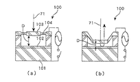
プロジェクタなどにおいて、所望の画像を形成する画像表示装置として、高速で光をオンオフ可能なDMDなどの光スイッチングデバイスが知られている。さらに、DMDのように反射性のミラーの角度を変えて光をオンフオフするものではなく、反射性のミラーと半透過性のミラーを用い、それらの距離を変えて光を制御する干渉型のデバイスが検討されている。図8(a)および(b)に示す干渉型表示素子は初澤ら(T.IEE Japan, Vol,119-E, No 12,'99,pp631-635)が提案しているものである。この干渉型のデバイス100は、シリコン基板101に高反射性のミラー(底部ミラー)102を設け、この底部ミラー102の上に適当な間隔Dを空けてハーフミラー103を設けたものである。このハーフミラー103は、ギャップ間隔を開けるSiO2などの部材がシリコン基板101との間に配置されている。
【0003】
この干渉型素子100は、図8(b)に示すように、ハーフミラー103は透明電極104を兼ねており、適当な電圧が印加されると基板101の側の底部ミラー102と上方のハーフミラー103との間に静電吸引力が働く。したがって、ハーフミラー103の位置が上下方向に制御され、ハーフミラー103と底部ミラー102との光路差が半波長(λ/2)ずれるに従って干渉が起こり、明暗のコントラスト変化が起こる。例えば、波長λの単色光を用いた場合は、ハーフミラー103が上下し、底部ミラー102との距離Dがλ/4変化すると明暗の変化が起こる。したがって、白色光を用いて、上下に動くハーフミラー103の位置を高精度に制御すれば、干渉色によりカラー表示も可能となる。このため、この干渉型素子100を多数集積すると、反射型のディスプレーを構成できる。そして、従来の白色光を3原色の各色光に時分割するカラーフィルタなどを用いるカラー表示方法に比べて、画素の集積度が約3倍に向上することが期待されている。また、液晶の代わりに、機械要素であるミラーにすることで、高速な応答が可能であり、さらに、静電駆動を用いることで、消費電力を低減できることも期待されている。
【0004】
【発明が解決しようとする課題】
このように、光干渉型素子を用いたデバイスは、従来の液晶デバイスより小型化が容易であり、さらに高速応答が可能で消費電力も少ないといった多くのメリットを備えている。しかしながら、上記の干渉型のデバイス100は実用化に向けて多くの問題を抱えている。その1つは、スイッチングする色毎にミラーの移動距離を変える必要があり、さらに、その距離をミクロン単位で制御する必要があることである。たとえば、上記のデバイスでは、ハーフミラー103が上下してスイッチングするが、底部ミラー102との距離Dがλ/4変化すると明暗の変化が起こる。したがって、底部ミラー102の距離をスイッチングする光の波長の1/4の距離で精度良く制御する必要がある。そして、スイッチングする光の波長が異なれば、距離Dを変える必要があり、3原色をスイッチングするためには少なくとも3種類の移動距離の異なる光スイッチング素子を1つのデバイスに作り込むか、あるいは、1つの光スイッチング素子の移動距離を3つの異なる距離に制御する必要がある。このため、非常に高い寸法精度が要求されることになり、実際に歩留まり良く製造することは困難である。
【0005】
上記のデバイスのように、オフ位置と、オン位置とをそれぞれ波長によって変化させる代わりに、オフ位置は固定してオン位置だけをスイッチングする波長で変えることにより、ミラーが動く距離の制御を簡易にすることが考えられる。しかしながら、オン位置の精度は、各々の波長の1/4の距離での精度、すなわち、数10nmあるいはnm程度さらにはそれ以下の精度が要求され、スイッチングする波長の異なる光スイッチング素子を同一のデバイスに作り込んだり、1つの光スイッチング素子でスイッチングする距離をnmレベルで制御することが要求される。したがって、光干渉型の光スイッチング素子は、サブミクロンオーダでの寸法精度に加えて、マルチカラーを表現するデバイスを実現するためには、寸法の異なる光スイッチング素子を1つのデバイスに作り込む必要があるので、構造が複雑になり製造上の問題が多い。このため、歩留りの向上、およびスイッチングの信頼性を向上させることが難しい。
【0006】
そこで、本発明においては、光干渉型のデバイスでありながら、量産性が高く、さらに、低コストで提供できる光スイッチング素子およびデバイスを提供することを目的としている。さらに、光スイッチング素子の制御回路も組み込むことができる光スイッチングデバイスおよびその製造方法を提供することを目的としている。また、本発明の光干渉型のデバイスを用いて低コストで高解像度のカラー表示が可能な画像表示装置を提供することも本発明の目的としている。
【0007】
【課題を解決するための手段】
このため、本発明においては、各色の光の波長毎に距離を変えるのではなく、1つの距離で各色の波長をオンオフする光干渉型の光スイッチング素子およびデバイスを提供するようにしている。すなわち、オフ位置のみならず、オン位置も各色の光の波長に共通な光スイッチング素子およびデバイスを提供する。このため、本発明の、半透過体と反射体との距離を変えることにより半透過体に入射した光をオンオフ可能な光スイッチング素子においては、反射体が半透過体に密着するオン位置と、反射体が半透過体から所定の距離だけ離れるオフ位置とに移動する。
【0008】
本発明の光スイッチング素子は、反射体と半透過体とを備えた干渉型であるが、モノクロでオンオフを制御する光スイッチング素子であり、反射体がハーフミラー、すなわち半透過体に密着して全反射するオン位置と、反射体が半透過体から所定の距離だけ離れて干渉によって出射される光をオフするオフ位置とを有する。したがって、オフする位置を、各波長の光を干渉によりほぼオフにできる位置に選択することにより、可視光領域の波長の光を1つの反射体の移動距離でスイッチングすることができる光スイッチング素子を提供できる。このため、この光スイッチング素子を2次元に並べた光スイッチングデバイスを画像の形成のために採用し、その光スイッチングデバイスに入射される色を分割することにより、マルチカラーの画像を出力可能な画像表示装置を提供できる。特に、本発明の光スイッチングデバイスと、カラーフィルタとを有する直視型の画像表示装置、あるいは本発明の光スイッチングデバイスと、この光スイッチングデバイスに各色の光を順番に供給する照明機構と、光スイッチングデバイスから出力された光をスクリーン上に投影するレンズとを有する画像表示装置は、単板式でマルチカラーの画像を表示することが可能である。そして、本発明の光スイッチングデバイスは、波長の異なる光を干渉により制御するために、寸法の異なる光スイッチング素子を1つのデバイスに作り込む必要はないので、構造が簡易となり、製造が容易となる。このため、本発明により歩留りを向上でき、信頼性の高い光スイッチングデバイスを低コストで提供できる。
【0009】
可視光領域の光をオフする位置は、反射体と半透過体との間の光路に沿った距離が100nmから150nmの範囲とすることが望ましい。光路が反射体に垂直であれば反射体と半透過体との距離を上記の範囲にすれば良いが、光路が傾いている場合は、その光路に沿った距離を上記の範囲にすることが望ましい。この範囲であれば、各色の波長を含む入射光、すなわち、420nmから620nmの波長の光の強度をほぼ30%以下にすることが可能であり、10対3のコントラストを確保することができる。したがって、さらに高コントラストが要求される場合は、複数の光スイッチングデバイスを設け、第1の光スイッチングデバイスから出射された光が第2の光スイッチングデバイスの入射光となるように配置することにより、高コントラストの画像を出力する画像表示装置を提供できる。また、デバイスのレベルで、複数の光スイッチング素子が、第1の光スイッチング素子の出射光が第2の光スイッチング素子の入力となるように直列に配置しても良い。
【0010】
さらに、可視光領域の光をオフする位置は、反射体と半透過体との間の光路に沿った距離が125nmから135nmの範囲とすることが望ましい。この範囲であれば、420nmから620nmの波長の光の強度をほぼ10%以下にすることが可能であり、10対1のコントラストを確保することができる。また、さらに高コントラストが要求される場合には、直列に配置するデバイスあるいは素子の数を低減することが可能となる。
【0011】
本発明の光スイッチング素子およびデバイスにおいては、オン位置で全ての波長の光を、高い強度で出射できるように反射体を半透過体に密着させる。したがって、反射体をオフ位置に駆動し易くするためには、反射体の半透過体に接する側、または半透過体の反射体に接する側に吸着防止層を形成することが望ましい。吸着防止層としては、ITO(Indium tin oxide)などの透明導電膜をコーティングすることができる。
【0012】
本発明の光スイッチング素子は、第1の基板に半透過体を形成し、第2の基板に反射体と、反射体をオン位置およびオフ位置に移動する複数のアクチュエータとを重ねて形成し、これら第1および第2の基板、半透過体と反射体とが対面し、オン位置では、反射体が半透過体に密着し、オフ位置では、反射体が半透過体から所定の距離だけ離れるように、第1および第2の基板を組み立てることが望ましい。また、光スイッチングデバイスであれば、第1の基板に複数の半透過体を形成し、第2の基板に複数の反射体と、各々の反射体をオン位置およびオフ位置に移動する複数のアクチュエータとを重ねて形成した後に、上記と同様のオン位置およびオフ位置となるように、第1および第2の基板を組み立てることが望ましい。
【0013】
干渉型の光スイッチングデバイスの半透過体と、反射体とを1つの基板上に配置するのではなく、異なる基板に配置して、それらの基板を合わせることにより干渉型のデバイスを構成し、さらに、反射体を、半透過体と反射体との距離(位置)を制御するアクチュエータに重ねて形成することにより、半透過体および反射体の機能をアクチュエータの機能と分離し、それぞれを最適化できる。また、透過体および反射体を別基板で製造するので、それぞれの構造体を製造する歩留まりが、分散あるいは独立となり、これらを1つの基板に作成していたときのように歩留まりが重なって、光スイッチング素子あるいは光スイッチングデバイスの歩留まりが低下するのを防止できる。このため、低コストで性能の良い、干渉型の光スイッチング素子および光スイッチングデバイスを提供することができる。
【0014】
このような構成および製造方法の光スイッチングデバイスであれば、反射体は、アクチュエータを兼ねる必要がないため、アクチュエータにはピエゾなどを用いることも可能である。これに対して、電極を積層する静電型のアクチュエータであれば、フォトリソグラフィー技術を用いて、サブミクロンオーダのサイズで製造することができる。さらに、消費電力が低くなる等のメリットもあるので適している。
【0015】
また、静電型のアクチュエータにおいては、オフ位置で第1および第2の電極の距離が最小となる。したがって、これらの電極の最小間隔を設定するストッパーを形成することにより、上述した特定の光路差、すなわち、100nm〜150nm、あるいは125nm〜135nmの距離にオフ位置を確実に制御でき、これを超えるようなオーバランを防止できる。また、ストッパーで停止する機構とすることにより、反射体が途中で止まらずにオフ位置まで確実に駆動できるような力を静電型アクチュエータで発揮する構成にでき、オフ位置の制御が簡易となる。
【0016】
さらに、第2の基板に対してアクチュエータにより駆動される光学素子が反射型であるので、第2の基板は透明である必要はない。したがって、第2の基板としてシリコン基板などの半導体回路を形成するが容易で実績のある基板を用いることができる。このため、半導体基板を用いて、この半導体基板にアクチュエータを積層し、各々の光スイッチング素子を駆動する制御回路を第2の基板に組み込むことが容易であり、駆動回路付きの光干渉型の光スイッチングデバイスを低コストで提供することができる。
【0017】
このように、本発明の光スイッチングデバイスであれば、構造が単純になるので、歩留まりが向上し量産性が増す。また、本発明の光スイッチングデバイスは反射型なので、上述したように、反射型の液晶パネルと同様の直視型の画像表示装置を提供できる。そして、液晶パネルより高速で、高解像度であり、さらに、消費電力も少ない画像表示装置を提供でき、携帯電話などの表示パネルとして採用することが可能である。
【0018】
【発明の実施の形態】
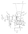
以下に図面を参照しながら本発明の実施の形態を説明する。図1に、本発明の光スイッチングデバイス4を備えたプロジェクタ装置1の概略構成を示してある。このプロジェクタ装置1は、光スイッチングデバイス4に、各色の光を順番に供給する照明機構2を備えている。本例の照明機構2は、キセノンランプなどの白色光71Wを出力する光源部2aと、この光源部2aからの白色の光束71Wを時分割する回転式のカラーフィルタ2bと、ここから照射される各色の光束71R、71Gまたは71Bを、直角に反射可能なビームスプリッタ3とを備えている。
【0019】
カラーフィルタ2bおよびビームスプリッタ3の光路上には、光束を平行化して導くコンデンサーレンズ2cと、たとえばS偏光の光束のみを通す偏光板7が配置されている。そして、偏光された各色の光束71R、71Gまたは71Bは、ビームスプリッタ3で垂直に光スイッチングデバイス4に反射される。光スイッチングデバイス4は光スイッチング素子が2次元に配置されており、各々がオンオフして画像を形成する。ビームスプリッタ3とデバイス4との間には、1/4波長板(白色用)8が設置されており、光スイッチングデバイス4でオンオフされた画像を形成する各色の光72R、72Gまたは72BはP偏光になり、ビームスプリッタ3を通過する。そして、レンズシステム6に達し、スクリーン7に投写されてカラー画像が表れる。なお、本例では、本図および以下の図において、赤色の光71Rがオンオフされる様子を図示するが、他の緑色の光71Gおよび青色の光71Bも同様である。また、S偏光およびP偏光は逆にしても、もちろん良い。
【0020】
本例の光スイッチングデバイス4は、、すなわちハーフミラーと反射体とを備えた光スイッチング素子が2次元に配列された干渉型のスイッチングデバイス4であり、各々の光スイッチング素子を駆動する回路を内蔵している。したがって、制御機構5から供給された画像データφに従って駆動回路が個々の画素を表示する光スイッチング素子をスイッチングし、画像表示デバイスであるスイッチングデバイス4により変調された表示光72が出力される。
【0021】
図2に、本例の光スイッチングデバイス4の概略構成を模式的に示してある。
本例の光スイッチングデバイス4は、第2の基板となる半導体基板31と、この半導体基板31に重ねられた第1の基板となるほぼ透明なガラス基板21とを有し、このガラス基板21の下方の面(表面)21aに、ハーフミラー22あるいはハーフミラー膜22aが形成されている。さらに、その表面にITOなどの透明導電膜がコーティングされて吸着防止膜25が形成されている。
【0022】
一方、半導体基板31は、その上方の面(表面)31aに、静電型のアクチュエータ33と反射体42とが基板31の側(下側)からこの順番で積層されている。アクチュエータ33は2次元に配列されており、また、アルミニウム製の反射体42も、各々の反射体42がアクチュエータ33により上下方向に駆動されるように2次元に配列されている。したがって、個々の反射体42は、個々のアクチュエータ33に連結されており上下に動く。
【0023】
アクチュエータ33は、静電駆動型であり、反射体42が機械的に連結された上電極34と、この上電極34と対峙するように基板の表面31aに形成された下電極35を備えている。上電極34は、弾性部材としての機能を備えており、電極34および35の間で静電力(静電吸引力)が働かないときは、弾性力によって反射体42を上方に加圧する。また、半導体基板31には、これらのアクチュエータ33を駆動する駆動回路(制御回路)38、さらには必要に応じてメモリなどが作り込まれている。
【0024】
上側の面31aに反射体42が形成された半導体基板31と、下側の面21aにハーフミラー22が形成されたガラス基板21とは、反射体42の反射面41とハーフミラー22の下面(ハーフミラーの表面)22aとが向かい合うように組み合わされており、それらの距離は基板31の周囲、またはアクチュエータ33の間に形成され壁39によって一定に保持されている。さらに、下電極35の周囲には、上方に突き出た形状の突起50が形成され、上電極34には突起50に対峙する位置にディンプル51が形成されており、これらにより、上電極34と下電極35との最小距離を正確に確保するストッパー52が構成されている。このため、上電極34と下電極35が最も近づいたときに、ハーフミラー22と反射体42とは最も離れて距離d1となるが、その距離d1が精度良く実現でき、オーバランも防止することができる。一方、半導体基板31とガラス基板21との距離は、上電極34と下電極35と離れたときに、上電極34のばね弾性で反射面41がハーフミラー22に密着するような距離に設定されている。このため、その位置では、ガラス基板21に入射した光をアルミニウム製の反射面41により高い反射率で光をほぼ垂直に反射することができる。
【0025】
このように本例の光スイッチングデバイス4は、半導体基板31の上にアクチュエータ33と、反射体42と、ハーフミラー22を備えた透明基板21とが積層された構成となっており、半導体基板31に作り込まれた駆動回路38と、アクチュエータ33と、反射体42と、これに対面するハーフミラー22によって1つの光スイッチング素子10が形成されている。さらに、光スイッチングデバイス4の全体に複数の光スイッチング素子10が2次元方向にアレイ状に配置あるいは集積された形態となっており、各々の光スイッチング素子が画像を形成する単位である画素に対応させて制御することにより2次元画像を表現できる。
【0026】
図2の左側に示した光スイッチング素子10aはオフ状態であり、図2の右側に示した光スイッチング素子10bはオン状態である。本例の光スイッチング素子10では、駆動回路38により、アクチュエータ33を構成する電極34および35の間に適当な駆動電圧が印加されると、アクチュエータ33の下電極35と上電極34との間で静電力が働き、反射体42が下方向に駆動される。このため、反射体42の反射面41と、対面するガラス基板21の上のハーフミラー22とが離れて距離d1となる。この距離d1は、ハーフミラー22により反射された可視光と、反射体42により反射された可視光とが干渉して弱め合う距離になっており、この状態、すなわち、光スイッチング素子10aの状態がオフ状態である。
【0027】
一方、駆動回路38により駆動電圧が印加されなくなると、上電極34の弾性によって反射体42は上方向に駆動される。このため、反射体42とハーフミラー22は密着し、反射面41により反射された光とハーフミラー22で反射された光の間には、干渉がないので入射光は略そのまま出射される。したがって、光スイッチング素子10bの状態がオン状態である。
【0028】
このように、本例の光スイッチングデバイス4では、アクチュエータ33に供給される駆動電圧を制御することにより、各々の光スイッチング素子10をオンオフすることが可能である。
【0029】
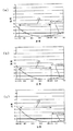
図3ないし図5に、オフ位置おける反射体42とハーフミラー22との距離(光路差)d1を変えたときの可視領域における各波長(400nm〜700nm)の強度を示している。
【0030】
図3(a)は、オフ位置の距離d1を125nmとしたときに、本例の光スイッチングデバイス4から出射される光の強度であり、図3(b)は、距離d1を130nm、図3(c)は、距離d1を135nmとしたときの強度である。等色関数を考慮すると、青色の光の感度が急激に上昇する波長420nmから、赤色の光の感度が急激に低下する波長620nmの範囲を可視光CRの範囲とし、この範囲の波長の光を干渉によって強度を十分に下げることができれば、オフ位置で可視光をオフできると考えてよい。これらの図3(a)〜(c)から分るように、上記の距離d1(125〜135nm)にオフ位置を設定すると、420nmから620nmの範囲の波長の光の強度を0.1以下に弱めることができる。したがって、オン位置で入射された光が全て反射されると考えると、オフ位置の距離d1を125nm〜135nmの範囲、すなわち、130±5nmの範囲とすることによりオンオフのコントラスト比10:1以上を得ることができる。
【0031】
これに対して、図4(a)にはオフ位置の距離d1を100nmとしたとき、図4(b)には距離d1を110nmとしたとき、および、図4(c)には距離d1を120nmとしたときに本例の光スイッチングデバイス4から出射される光の強度を示してある。これらの図から分るように、距離d1が120nmから100nmの範囲では、可視光領域CRの光の強度は最高で0.3程度になる。したがって、この範囲であっても10:3程度のコントラスト比を確保することができる。しかしながら、長波長領域、すなわち赤色側での反射光の強度が高くなってしまい、10:1程度あるいはそれ以下のコントラスト比を得ることは難しくなる。
【0032】
また、図5(a)にはオフ位置での距離d1を140nmとした場合を、図5(b)には距離d1を145nmとした場合を、図5(c)には距離d1を150nmとした場合に本例の光スイッチングデバイス4から出射される光の強度を示してある。これらの図から分るように、距離d1が140nm以上になると、可視光領域CRの光の強度の最高は0.3程度になる。したがって、この範囲であっても10:3程度のコントラスト比を確保することができる。しかしながら、短波長領域、すなわち青色側での反射光の強度が高くなってしまい、10:1程度あるいはそれ以下のコントラスト比を得ることは難しくなる。
【0033】
このように、本例の光スイッチングデバイス4では、オフ位置における反射体42とハーフミラー22との距離d1を100nmから150nmにすることにより、10:3のコントラスト比を確保することができる。一方、距離d1を125nm〜135nmの範囲に設定することで、コントラスト比を10:1まで高めることが可能である。したがって、これらのコントラスト比が得られれば良い用途においては、本例の光スイッチングデバイス4を単独で使用することにより、画像を形成したり、それを投影することが可能である。一方、さらに高いコントラスト比が要求される用途においては、第1の光スイッチングデバイスあるいは光スイッチング素子から出力された光を第2の光スイッチングデバイスあるいは光スイッチング素子の入力として、さらにスイッチングするアレンジを採用する。これにより、コントラスト比を高くすることが可能であり、高コントラスト比が要求される用途の画像表示装置にも本発明の光スイッチング素子およびデバイスを適用することができる。
【0034】
そして、本例の光スイッチングデバイス4では、1つのオンオフの位置の組み合わせ、すなわち、オフ位置の距離d1が1つで、各色の光71R、71Gおよび71Bをオンオフすることができる。従来の光干渉型の光スイッチング素子においては、各色の光の波長λR、λGおよびλBに応じた距離dr、dgおよびdbをオン位置あるいはオフ位置にしていたのに対し、本例の光スイッチングデバイスでは、オン位置は距離が0、すなわち、反射体42とハーフミラー22が密着した位置とし、オフ位置における距離d1を上述した範囲に定めることにより、可視光領域CRの光を一括してオンオフすることができる。
【0035】
たとえば、コントラスト比を10:1に設定したとしても、本例の光スイッチングデバイス4は、全ての光スイッチング素子10のオフ位置d1を、130nmを中心に公差±5nm程度の範囲で製造することにより、設定条件をクリアできる。そして、照明機構2の側で各色の光を順番に光スイッチングデバイス4に供給することにより、全ての色の光を同一の条件、すなわち、移動距離d1でオンオフし、マルチカラーの画像を表示することができる。したがって、本例の光スイッチングデバイスは、干渉型の光スイッチングデバイスでありながら、寸法精度は緩やかで良く、高性能の光スイッチング素子およびデバイスの歩留まりを向上でき、品質の良い光スイッチングデバイスを低コストで供給できる。
【0036】
図6(a)〜(d)に、本例の光スイッチングデバイス4の製造プロセスの概要を示してある。まず、図6(a)に示すように、予め駆動回路38などがCMOS回路で作り込まれた半導体基板(第2の基板)31の表面31aに、アクチュエータ33を製造する。このプロセスは、図示していないが、シリコンなどの適当な材質の犠牲層を用いたフォトリソグラフィー技術を用いて製造できる。たとえば、先ず、基板の表面31aに電極層(Al膜)をディポジットし、パターニングして下電極35とバネを兼ねた上電極34の構造のアンカー部分36を形成する。さらに、下電極35の周囲に、上電極34のディンプル51に対応する位置に突起50を形成してストッパーを構成する。そして、不図示の犠牲層を挟み、この犠牲層の上にバネを兼ねた上電極34となる層(Al膜)をディポジットする。このAl層をパターニングして、上電極34およびそれを基板31で支持するポスト36を形成する。犠牲層の除去はいつのタイミングでも可能であるが、可動する上電極34を保護するため、素子分離などの最終段階で除去することが望ましい。
【0037】
次に、図6(b)に示すように、上電極34に機械的に支持されるようにアルミニウム製の反射体42を製造する。このプロセスは、アクチュエータ33に積層するように、上記と同様に犠牲層を用いたフォトリソグラフィー技術により反射体42を形成することも可能である。これにより、各画素の単位で反射体42をアクチュエータ33で上下に駆動する構造が形成される。このタイミングで、アクチュエータ33を構成するための犠牲層を含めて除去することもできる。なお、図示していないが、アクチュエータ33および反射体42を製造するプロセスと同時に、壁39も半導体基板31の上に製造する。
【0038】
一方、図6(a)および(b)に示した第2の基板である半導体基板31の上に構造物を製造する工程と前後して、あるいは同時に、図6(c)に示すように、第1の基板であるガラス基板21にハーフミラー22を形成するプロセスを行う。このプロセスでは、ガラス基板21の表面21aに、各画素の単位でハーフミラー22を形成する。あるいは、ガラス基板21の表面21aの全体にわたりハーフミラー22を形成しても良く、画素あるいは素子単位で駆動する反射体42と組み合わされることで、画素単位で制御できる光スイッチング素子を構成できる。ハーフミラー22は、例えば、フッ化マグネシウムや氷晶石などの屈折誘電体の1/4λの層と、硫化亜鉛などの高屈折誘電体の1/4λの層を交互に積層することにより形成できる。そして、画素単位で分離する場合は、エッチングなどの公知の方法を適用できる。
【0039】
さらに、ハーフミラー22の上面(ハーフミラー膜)22aを含むガラス表面21aに、ITOなどの透明導電膜を吸着防止用の膜25として設ける。ハーフミラー22の上面22aに反射体42の表面41が密着する際に、吸着防止層25を挟むことになる。この吸着防止層25は、反射面41とハーフミラーの表面22aを積極的に同電位(GND)にすることが可能である。このため、ハーフミラー22が電気的に浮いている場合でも、ハーフミラー22の表面22aがチャージアップし、このハーフミラーの表面22aと対向する反射面41とが静電吸着することを防止できる。したがって、反射体42を駆動するためのアクチュエータ33の消費電力を低減でき、また、反射体42の駆動速度を向上することができる。ITO層などの吸着防止膜25は、反射体42の側に設けても良い。
【0040】
そして、図6(d)に示すように、ハーフミラー22が形成されたガラス基板21と、アクチュエータ33および反射体42が形成された半導体基板31を、ハーフミラーの表面22aと反射面41とが対面するように組み合わせる。基板21および31との間隔は、光スイッチング素子10の周囲に形成された柱39により、上述したように、アクチュエータ33で反射体42をオフ位置へ駆動した際にハーフミラー22と反射体42と間が距離d1となり、オン位置で駆動したときに反射体42がハーフミラー22に密着するように設定する。
【0041】
このように、本例の光スイッチングデバイス4では、ハーフミラー22を第1の基板であるガラス基板21に設け、反射体42を第2の基板である半導体基板31に設けてある。ハーフミラー22と、反射体42とを異なる基板21および31の上に形成することにより、これらの基板21および31を並列で製造でき、製造工程を短縮し、また、簡略化できるだけでなく、光学的な特性も改善できるなどの多くのメリットがある。すなわち、図8を参考に説明したように、現在提案されている光干渉型の装置は1枚の基板上にスイッチング素子を構成しているために、電極と反射体あるいは半透過体とを兼ねた構造が要求されている。したがって、製造工程が複雑になったり、光学的な特性の改善が難しく、さらに駆動回路を容易には組み込めないといった欠点がある。
【0042】
これに対し、本例の光スイッチングデバイス4においては、まず、ハーフミラー22と反射体42とを別々の基板上に製造できるので、歩留まりが相乗されて悪化することがなく、極めて製造しやすい。そして、反射体42を別基板である半導体基板31で支持しているので、半導体基板31の上にアクチュエータ33を積層することが可能となり、アクチュエータ33として静電型に限らず、ピエゾなどのタイプも採用可能となる。そして、反射体42およびハーフミラー22が電極を兼用する必要が無くなるので、これらの両端が基板に固定されたり、支柱に固定されたりすることがない。したがって、スイッチングする間に撓んだり歪んだりする可能性が非常に低くなり、オフ位置で設定した距離d1となるように反射体42およびハーフミラー22を制御できる。このため、本例の光スイッチングデバイス4は、距離d1の公差も十分に確保できることもあり、所望の性能の光スイッチングデバイスを歩留まり良く製造することができる。
【0043】
また、第2の基板31は、反射体42の反対側に位置することになるので、透明基板である必要はなく、半導体基板として駆動回路を従来の半導体基板を製造するプロセスで作り込むことができる。また、反射体42の反射面41が第2の基板31の外面を向き、また、ハーフミラー22の面22aが外側を向くので、吸着防止膜を塗布するなどの処理がし易いなど、本例の光スイッチングデバイス4は反射性能の高い光スイッチングデバイスとするのに適した構成となっている。このように、本例の光スイッチングデバイス4は光干渉型でありながら、ハーフミラー22と反射体42とを別々の基板上に構成することにより、光干渉型の光スイッチング素子の各々の構成を最適化することが可能となっており、高性能の光スイッチングデバイス4を低コストで提供することができる。もちろん、基板(第の基板)31は、上記の半導体基板に限らず、アクチュエータ33を支持できる基板であれば、本発明の効果が得られる。
【0044】
そして、本例の光スイッチングデバイス4では、各色の波長毎にオンオフの位置を変える必要がないので、複数のアレイ状に配置された光スイッチング素子10を、全て同じで比較的単純な構成で形成できる。つまり、各色の波長に応じた距離となるように、ハーフミラーと反射体の距離および電極間の距離を複雑に制御あるいは設計・製造する必要はなく、スイッチングする光の波長に依存しない構造を採用でき、アクチュエータの制御においても光の波長に依存しない条件でオンオフできる。この点においても、構造を簡略化でき、さらに信頼性の高い光スイッチングデバイス4を提供できる。このため、光スイッチングデバイス4の寸法上の制約を緩め、製造の容易化を実現でき、量産性のある光スイッチングデバイス4を提供できる。
【0045】
なお、上記では、光スイッチングデバイス4に対し垂直に光が入射する画像表示装置を例に説明しているが、斜めに光が入射して出力される光スイッチングデバイスに対しても本発明を適用することができる。この場合は、その入射および出射光路に沿った距離を上記のd1の範囲に設定することが望ましい。
【0046】
また、照明機構2において、回転型のカラーフィルタ2bを採用し、これにより時分割して所望の色を光スイッチングデバイス4に照射する例を示しているが、これに限られない。例えば、光源部に各色のLEDを用いて、各色の光を順番に光スイッチングデバイスに照射できる照明機構であれば良い。また、単板式に限らず、同一の構成、すなわち、オフ位置が同じ光スイッチングデバイスを3組用いてダイクロイックミラーを用いた光学系と組み合わせて3板式のプロジェクタを構成することも可能である。
【0047】
さらに、図3ないし5に示したように、波長が420nm〜620nmの範囲を超えるとコントラスト比が悪化する傾向になるので、照明機構2において、白色光を色分離すると共に、ダイクロイックミラーあるいはプリズムを用いて420nm以下の波長の光や、620nm以上の波長の光をカットして光スイッチングデバイス4に照射し、コントラスト比を向上させることも可能である。
【0048】
また、上記では、光スイッチング素子10をアレイ状に並列に配置した例を示しているが、複数の光スイッチング素子10あるいは光スイッチングデバイス4を用いて、光をシリーズに変調し、コントラスト比を向上できることは上述した通りである。
【0049】
さらに、本発明のスイッチングデバイス4は反射型なので、図7に示すように、カラーフィルタ81を重ねて配置し、用いて反射型の液晶パネルと同様の直視型の画像表示装置80を提供できる。そして、液晶パネルより高速で、高解像度であり、さらに、消費電力も少ない画像表示装置を提供でき、携帯電話などの表示パネルとして採用することが可能である。
【0050】
【発明の効果】
以上に説明したように、本発明においては、オン位置で反射体と半透過体が密着し、オフ位置で反射体と半透過体とを可視光領域の光を干渉でオフできる距離にしている。特に、オフ位置の距離を130nm±5nm程度にすることにより、10:1というコントラストを実現できる。このため、本発明により、干渉型の光スイッチングデバイスにおいて、その寸法上の制約を緩め、製造を容易にでき、信頼性の高い光スイッチングデバイスを低コストで提供できる。
【0051】
さらに、本発明は、ハーフミラー、すなわち半透過体と反射体との距離を制御する干渉型の光スイッチングデバイスに関するものであり、半透過体と、反射体とを異なる基板に形成することにより、歩留まりが相乗されて製品不良が増加するのを防止することができるなどの製造上のメリットを得ることができる。それと共に、反射体を別基板である半導体基板で支持することにより、反射体とアクチュエータとしての機能を分離することが可能となり、光学的性能を向上しやすく、さらに、半導体基板に駆動回路を組み込むことができるなどの上記にて開示した多種多様の効果を得ることができる。このため、本発明により、歩留りの高い、またスイッチングの信頼性も高い光スイッチングデバイスを提供できる。
【図面の簡単な説明】
【図1】本発明に係る光スイッチングデバイスを用いたプロジェクタ装置の概要を示す図である。
【図2】図1に示す光スイッチングデバイスにおける光スイッチング素子のオン状態またはオフ状態を示す図である。
【図3】図2に示す、反射体およびハーフミラーとの距離d1が125nm〜135nmの範囲の光スイッチングデバイスから出射される光の波長と強度との関係を示すグラフである。
【図4】図2に示す、反射体およびハーフミラーとの距離d1が100nm〜120nmの範囲の光スイッチングデバイスから出射される光の波長と強度との関係を示すグラフである。
【図5】図2に示す、反射体およびハーフミラーとの距離d1が140nm〜150nmの範囲の光スイッチングデバイスから出射される光の波長と強度との関係を示すグラフである。
【図6】図2に示す光スイッチングデバイスの製造プロセスを模式的に示す図である。
【図7】本発明に係る光スイッチングデバイスを用いた直視型の表示装置の概要を示す図である。
【図8】従来の干渉型の光スイッチングデバイスの一例を示す概略図である。
【符号の説明】
1 プロジェクタ
2 照明機構
2a 白色光源、2b カラーフィルタ、2c コンデンサーレンズ
3 ビームスプリッタ
4 光スイッチングデバイス
5 制御機構
6 投写レンズ
7 スクリーン
10 光スイッチング素子
21 ガラス基板(第1の基板)
22 ハーフミラー、22a ハーフミラーの表面
25 吸着防止層
31 半導体基板(第2の基板)
33 アクチュエータ
34 上電極
35 下電極
38 駆動回路
39 壁(支柱)
41 反射面
42 反射体
50 ストッパー
71 入射光
72 出力される表示光[0001]
BACKGROUND OF THE INVENTION
The present invention relates to an optical switching element, an optical switching device, and a manufacturing method thereof used for a direct-view image display apparatus or a projector apparatus.
[0002]
[Prior art]
2. Description of the Related Art An optical switching device such as a DMD that can turn on and off light at high speed is known as an image display device that forms a desired image in a projector or the like. Furthermore, an interference type device that uses a reflective mirror and a semi-transparent mirror to control the light by changing the distance between them instead of changing the angle of the reflective mirror as in DMD. Is being considered. The interference type display elements shown in FIGS. 8A and 8B are proposed by Hatsuzawa et al. (T. IEE Japan, Vol. 119-E, No. 12, '99, pp 631-635). In this
[0003]
In this
[0004]
[Problems to be solved by the invention]
As described above, a device using an optical interference type element has many merits that it is easier to miniaturize than a conventional liquid crystal device, can respond faster, and consumes less power. However, the
[0005]
Instead of changing the OFF position and ON position according to the wavelength as in the above device, the OFF position is fixed, and only the ON position is changed with the wavelength that switches, so the control of the distance the mirror moves can be simplified. It is possible to do. However, the accuracy of the ON position is required at a distance of ¼ of each wavelength, that is, an accuracy of several tens of nanometers or nanometers or less, and optical switching elements having different wavelengths to be switched are connected to the same device. Or the distance to be switched by one optical switching element is required to be controlled at the nm level. Therefore, in addition to the dimensional accuracy in the sub-micron order, the optical interference type optical switching element needs to incorporate optical switching elements having different dimensions into one device in order to realize a device expressing multicolor. As a result, the structure becomes complicated and there are many manufacturing problems. For this reason, it is difficult to improve the yield and the switching reliability.
[0006]
Accordingly, an object of the present invention is to provide an optical switching element and a device that can be provided at a low cost while being a light interference type device, with high mass productivity. Furthermore, it aims at providing the optical switching device which can also incorporate the control circuit of an optical switching element, and its manufacturing method. It is another object of the present invention to provide an image display apparatus capable of high-resolution color display at low cost using the optical interference type device of the present invention.
[0007]
[Means for Solving the Problems]
For this reason, the present invention provides an optical interference type optical switching element and device that does not change the distance for each wavelength of light of each color, but turns on and off the wavelength of each color by one distance. In other words, not only the off position but also the on position provides an optical switching element and device common to the wavelengths of light of each color. For this reason, in the optical switching element capable of turning on and off the light incident on the semi-transmissive body by changing the distance between the semi-transmissive body and the reflective body of the present invention, the ON position where the reflective body is in close contact with the semi-transmissive body, The reflector moves to an off position that is a predetermined distance away from the translucent body.
[0008]
The optical switching element of the present invention is an interference type comprising a reflector and a semi-transmissive body, but is an optical switching element that controls on / off in monochrome, and the reflector is in close contact with a half mirror, that is, a semi-transmissive body. An on position where the light is totally reflected and an off position where the light is emitted by interference with the reflector away from the translucent body by a predetermined distance. Therefore, an optical switching element that can switch light of a wavelength in the visible light region by a moving distance of one reflector by selecting a position where the light of each wavelength can be almost turned off by interference is selected. Can be provided. For this reason, an optical switching device in which the optical switching elements are arranged two-dimensionally is used for image formation, and an image capable of outputting a multicolor image by dividing the color incident on the optical switching device. A display device can be provided. In particular, a direct-view image display device having the optical switching device of the present invention and a color filter, or the optical switching device of the present invention, an illumination mechanism for sequentially supplying light of each color to the optical switching device, and optical switching An image display apparatus having a lens that projects light output from a device onto a screen can display a multi-color image with a single plate. In the optical switching device of the present invention, since it is not necessary to make optical switching elements having different dimensions in one device in order to control light having different wavelengths by interference, the structure becomes simple and the manufacture becomes easy. . Therefore, the yield can be improved by the present invention, and a highly reliable optical switching device can be provided at low cost.
[0009]
As for the position where the light in the visible light region is turned off, it is desirable that the distance along the optical path between the reflector and the semi-transmissive body is in the range of 100 nm to 150 nm. If the optical path is perpendicular to the reflector, the distance between the reflector and the semi-transmissive body may be in the above range, but if the optical path is inclined, the distance along the optical path may be in the above range. desirable. Within this range, it is possible to reduce the intensity of incident light including wavelengths of the respective colors, that is, light having a wavelength of 420 nm to 620 nm, to approximately 30% or less, and 10 to 3 contrast can be ensured. Therefore, when a higher contrast is required, by providing a plurality of optical switching devices and arranging the light emitted from the first optical switching device to be incident light of the second optical switching device, An image display device that outputs a high-contrast image can be provided. Further, at the device level, the plurality of optical switching elements may be arranged in series so that the light emitted from the first optical switching element becomes the input of the second optical switching element.
[0010]
Furthermore, it is desirable that the position where the light in the visible light region is turned off be in the range of 125 nm to 135 nm along the optical path between the reflector and the semi-transmissive body. Within this range, the intensity of light having a wavelength of 420 nm to 620 nm can be made approximately 10% or less, and a 10: 1 contrast can be secured. In addition, when a higher contrast is required, the number of devices or elements arranged in series can be reduced.
[0011]
In the optical switching element and device of the present invention, the reflector is brought into close contact with the semi-transmitter so that light of all wavelengths can be emitted with high intensity at the on position. Therefore, in order to facilitate driving the reflector to the off position, it is desirable to form an anti-adsorption layer on the side of the reflector that contacts the semi-transmitter or the side of the semi-transmitter that contacts the reflector. As the adsorption preventing layer, a transparent conductive film such as ITO (Indium tin oxide) can be coated.
[0012]
The optical switching element of the present invention is formed by forming a translucent body on a first substrate, a reflector on a second substrate, and a plurality of actuators that move the reflector to an on position and an off position, The first and second substrates, the semi-transmitter and the reflector face each other, the reflector is in close contact with the semi-transmitter in the on position, and the reflector is separated from the semi-transmitter by a predetermined distance in the off position. Thus, it is desirable to assemble the first and second substrates. Further, in the case of an optical switching device, a plurality of semi-transparent bodies are formed on a first substrate, a plurality of reflectors are formed on a second substrate, and a plurality of actuators move each reflector to an on position and an off position. It is desirable to assemble the first and second substrates so that the same ON position and OFF position as described above are obtained.
[0013]
The interference-type optical switching device transflector and the reflector are not arranged on one substrate, but are arranged on different substrates, and the substrates are combined to form an interference-type device. By forming the reflector over the actuator that controls the distance (position) between the semi-transparent and the reflector, the functions of the semi-transparent and the reflector can be separated from the functions of the actuator, and each can be optimized. . In addition, since the transmission body and the reflection body are manufactured on different substrates, the yields for manufacturing the respective structures are dispersed or independent, and the yields are overlapped as if they were formed on one substrate, and the light It is possible to prevent the yield of switching elements or optical switching devices from decreasing. Therefore, it is possible to provide an interference-type optical switching element and an optical switching device that are low in cost and good in performance.
[0014]
In the case of the optical switching device having such a configuration and manufacturing method, the reflector does not need to also serve as an actuator, and therefore, a piezo or the like can be used for the actuator. On the other hand, an electrostatic actuator in which electrodes are stacked can be manufactured in a submicron order size using a photolithography technique. Furthermore, there is a merit such as low power consumption, which is suitable.
[0015]
In the electrostatic actuator, the distance between the first and second electrodes is minimized at the off position. Therefore, by forming a stopper that sets the minimum distance between these electrodes, the off position can be reliably controlled to the specific optical path difference described above, that is, a distance of 100 nm to 150 nm, or 125 nm to 135 nm, and so on. Overrun can be prevented. In addition, by using a mechanism that stops with a stopper, it is possible to configure the electrostatic actuator to exert a force that can reliably drive the reflector to the off position without stopping midway, and the off position can be easily controlled. .
[0016]
Furthermore, since the optical element driven by the actuator with respect to the second substrate is a reflection type, the second substrate does not need to be transparent. Therefore, although a semiconductor circuit such as a silicon substrate can be formed as the second substrate, an easy and proven substrate can be used. Therefore, using a semiconductor substrate, it is easy to stack an actuator on the semiconductor substrate and incorporate a control circuit for driving each optical switching element into the second substrate. A switching device can be provided at low cost.
[0017]
As described above, the optical switching device of the present invention has a simple structure, thereby improving yield and increasing mass productivity. Further, since the optical switching device of the present invention is a reflection type, as described above, a direct-view type image display device similar to a reflection type liquid crystal panel can be provided. An image display device that is faster and has higher resolution than a liquid crystal panel and consumes less power can be provided, and can be used as a display panel for a mobile phone or the like.
[0018]
DETAILED DESCRIPTION OF THE INVENTION
Embodiments of the present invention will be described below with reference to the drawings. FIG. 1 shows a schematic configuration of a
[0019]
On the optical path of the
[0020]
The optical switching device 4 of this example is an interference-type switching device 4 in which optical switching elements each having a half mirror and a reflector are two-dimensionally arranged, and has a built-in circuit for driving each optical switching element. is doing. Therefore, the drive circuit switches the optical switching element that displays each pixel in accordance with the image data φ supplied from the control mechanism 5, and the display light 72 modulated by the switching device 4 that is an image display device is output.
[0021]
FIG. 2 schematically shows a schematic configuration of the optical switching device 4 of this example.
The optical switching device 4 of this example includes a
[0022]
On the other hand, the
[0023]
The
[0024]
The
[0025]
As described above, the optical switching device 4 of this example has a configuration in which the
[0026]
The
[0027]
On the other hand, when the drive voltage is no longer applied by the
[0028]
Thus, in the optical switching device 4 of this example, each optical switching
[0029]
3 to 5 show the intensities of the respective wavelengths (400 nm to 700 nm) in the visible region when the distance (optical path difference) d1 between the
[0030]
3A shows the intensity of light emitted from the optical switching device 4 of this example when the distance d1 of the off position is 125 nm, and FIG. 3B shows the distance d1 of 130 nm. (C) is the intensity when the distance d1 is 135 nm. Considering the color matching function, the range from the
[0031]
On the other hand, when the distance d1 of the off position is 100 nm in FIG. 4A, the distance d1 is 110 nm in FIG. 4B, and the distance d1 is shown in FIG. 4C. The intensity of light emitted from the optical switching device 4 of this example when the thickness is 120 nm is shown. As can be seen from these figures, when the distance d1 is in the range of 120 nm to 100 nm, the light intensity in the visible light region CR is about 0.3 at the maximum. Accordingly, even in this range, a contrast ratio of about 10: 3 can be ensured. However, the intensity of reflected light in the long wavelength region, that is, the red side is increased, and it becomes difficult to obtain a contrast ratio of about 10: 1 or less.
[0032]
5A shows the case where the distance d1 at the off position is 140 nm, FIG. 5B shows the case where the distance d1 is 145 nm, and FIG. 5C shows that the distance d1 is 150 nm. In this case, the intensity of light emitted from the optical switching device 4 of this example is shown. As can be seen from these figures, when the distance d1 is 140 nm or more, the maximum light intensity in the visible light region CR is about 0.3. Accordingly, even in this range, a contrast ratio of about 10: 3 can be ensured. However, the intensity of reflected light in the short wavelength region, that is, the blue side is increased, and it becomes difficult to obtain a contrast ratio of about 10: 1 or less.
[0033]
Thus, in the optical switching device 4 of this example, the contrast ratio of 10: 3 can be ensured by changing the distance d1 between the
[0034]
In the optical switching device 4 of this example, the
[0035]
For example, even if the contrast ratio is set to 10: 1, the optical switching device 4 of this example is manufactured by manufacturing the OFF positions d1 of all the
[0036]
6A to 6D show an outline of the manufacturing process of the optical switching device 4 of this example. First, as shown in FIG. 6A, an
[0037]
Next, as shown in FIG. 6B, an
[0038]
On the other hand, as shown in FIG. 6C, before or after or simultaneously with the step of manufacturing the structure on the
[0039]
Further, a transparent conductive film such as ITO is provided as an
[0040]
6D, the
[0041]
As described above, in the optical switching device 4 of this example, the
[0042]
On the other hand, in the optical switching device 4 of this example, since the
[0043]
Further, since the
[0044]
In the optical switching device 4 of this example, since it is not necessary to change the on / off position for each wavelength of the color, the
[0045]
In the above description, the image display apparatus in which light is incident perpendicularly to the optical switching device 4 has been described as an example. However, the present invention is also applied to an optical switching device that outputs light by being incident obliquely. can do. In this case, it is desirable to set the distance along the incident and outgoing optical paths in the above range of d1.
[0046]
Moreover, although the rotation
[0047]
Further, as shown in FIGS. 3 to 5, since the contrast ratio tends to deteriorate when the wavelength exceeds the range of 420 nm to 620 nm, the
[0048]
Moreover, although the example which has arrange | positioned the
[0049]
Furthermore, since the switching device 4 of the present invention is a reflection type, as shown in FIG. 7, a direct-view
[0050]
【The invention's effect】
As described above, in the present invention, the reflector and the semi-transmitter are in close contact at the on position, and the reflector and the semi-transmitter are set at a distance at which light in the visible light region can be turned off by interference at the off position. . In particular, a contrast of 10: 1 can be realized by setting the distance of the off position to about 130 nm ± 5 nm. For this reason, according to the present invention, the interference-type optical switching device can be relaxed in terms of dimensions, can be easily manufactured, and a highly reliable optical switching device can be provided at low cost.
[0051]
Furthermore, the present invention relates to a half mirror, that is, an interference-type optical switching device that controls the distance between the semi-transparent body and the reflector, and by forming the semi-transparent body and the reflector on different substrates, It is possible to obtain manufacturing merits such as prevention of an increase in product defects due to a synergistic yield. At the same time, by supporting the reflector with a semiconductor substrate which is a separate substrate, it is possible to separate the functions of the reflector and the actuator, so that the optical performance can be easily improved, and a drive circuit is incorporated in the semiconductor substrate. A wide variety of effects disclosed above can be obtained. Therefore, according to the present invention, an optical switching device having a high yield and high switching reliability can be provided.
[Brief description of the drawings]
FIG. 1 is a diagram showing an outline of a projector apparatus using an optical switching device according to the present invention.
2 is a diagram showing an on state or an off state of an optical switching element in the optical switching device shown in FIG. 1;
3 is a graph showing the relationship between the wavelength and intensity of light emitted from an optical switching device having a distance d1 between a reflector and a half mirror in the range of 125 nm to 135 nm shown in FIG. 2;
4 is a graph showing the relationship between the wavelength and intensity of light emitted from an optical switching device in which the distance d1 between the reflector and the half mirror shown in FIG. 2 is in the range of 100 nm to 120 nm.
5 is a graph showing the relationship between the wavelength and intensity of light emitted from an optical switching device having a distance d1 between a reflector and a half mirror shown in FIG. 2 in a range of 140 nm to 150 nm. FIG.
6 is a diagram schematically showing a manufacturing process of the optical switching device shown in FIG. 2. FIG.
FIG. 7 is a diagram showing an outline of a direct-view display device using the optical switching device according to the present invention.
FIG. 8 is a schematic view showing an example of a conventional interference-type optical switching device.
[Explanation of symbols]
1 Projector
2 Illumination mechanism
2a white light source, 2b color filter, 2c condenser lens
3 Beam splitter
4 Optical switching devices
5 Control mechanism
6 Projection lens
7 screens
10 Optical switching element
21 Glass substrate (first substrate)
22 half mirror, 22a half mirror surface
25 Adsorption prevention layer
31 Semiconductor substrate (second substrate)
33 Actuator
34 Upper electrode
35 Lower electrode
38 Drive circuit
39 Wall (support)
41 reflective surface
42 Reflector
50 stopper
71 Incident light
72 Display light to be output
Claims (10)
前記光スイッチング素子は、2次元に複数配置されるとともに、波長が420〜620nmの範囲で各色の光が順番に供給され、前記反射体が前記半透過体に密着するオン位置と、前記反射体と前記半透過体との間の光路に沿った距離が100nmから150nmの範囲だけ離れるオフ位置とに移動する光スイッチング素子。An optical interference-type optical switching element capable of turning on and off the light incident on the semi-transmissive body by changing the distance between the semi-transmissive body and the reflective body,
A plurality of the optical switching elements are arranged two-dimensionally, light of each color is sequentially supplied in a wavelength range of 420 to 620 nm, and the reflector is in close contact with the transflector, and the reflector Switching element that moves to an off position in which the distance along the optical path between the semi-transparent material and the semi-transparent material is separated by a range of 100 nm to 150 nm.
Priority Applications (1)
| Application Number | Priority Date | Filing Date | Title |
|---|---|---|---|
| JP2001085749A JP3888075B2 (en) | 2001-03-23 | 2001-03-23 | Optical switching element, optical switching device, and image display apparatus |
Applications Claiming Priority (1)
| Application Number | Priority Date | Filing Date | Title |
|---|---|---|---|
| JP2001085749A JP3888075B2 (en) | 2001-03-23 | 2001-03-23 | Optical switching element, optical switching device, and image display apparatus |
Publications (3)
| Publication Number | Publication Date |
|---|---|
| JP2002287047A JP2002287047A (en) | 2002-10-03 |
| JP2002287047A5 JP2002287047A5 (en) | 2005-03-03 |
| JP3888075B2 true JP3888075B2 (en) | 2007-02-28 |
Family
ID=18941210
Family Applications (1)
| Application Number | Title | Priority Date | Filing Date |
|---|---|---|---|
| JP2001085749A Expired - Fee Related JP3888075B2 (en) | 2001-03-23 | 2001-03-23 | Optical switching element, optical switching device, and image display apparatus |
Country Status (1)
| Country | Link |
|---|---|
| JP (1) | JP3888075B2 (en) |
Families Citing this family (52)
| Publication number | Priority date | Publication date | Assignee | Title |
|---|---|---|---|---|
| US6674562B1 (en) | 1994-05-05 | 2004-01-06 | Iridigm Display Corporation | Interferometric modulation of radiation |
| US7550794B2 (en) | 2002-09-20 | 2009-06-23 | Idc, Llc | Micromechanical systems device comprising a displaceable electrode and a charge-trapping layer |
| WO1999052006A2 (en) | 1998-04-08 | 1999-10-14 | Etalon, Inc. | Interferometric modulation of radiation |
| US8928967B2 (en) | 1998-04-08 | 2015-01-06 | Qualcomm Mems Technologies, Inc. | Method and device for modulating light |
| TWI289708B (en) | 2002-12-25 | 2007-11-11 | Qualcomm Mems Technologies Inc | Optical interference type color display |
| TW570896B (en) | 2003-05-26 | 2004-01-11 | Prime View Int Co Ltd | A method for fabricating an interference display cell |
| US7342705B2 (en) | 2004-02-03 | 2008-03-11 | Idc, Llc | Spatial light modulator with integrated optical compensation structure |
| US7190434B2 (en) * | 2004-02-18 | 2007-03-13 | Asml Netherlands B.V. | Lithographic apparatus and device manufacturing method |
| US7855824B2 (en) | 2004-03-06 | 2010-12-21 | Qualcomm Mems Technologies, Inc. | Method and system for color optimization in a display |
| CA2575314A1 (en) | 2004-07-29 | 2006-02-09 | Idc, Llc | System and method for micro-electromechanical operating of an interferometric modulator |
| US7928928B2 (en) | 2004-09-27 | 2011-04-19 | Qualcomm Mems Technologies, Inc. | Apparatus and method for reducing perceived color shift |
| US7583429B2 (en) | 2004-09-27 | 2009-09-01 | Idc, Llc | Ornamental display device |
| US7898521B2 (en) | 2004-09-27 | 2011-03-01 | Qualcomm Mems Technologies, Inc. | Device and method for wavelength filtering |
| US7630123B2 (en) | 2004-09-27 | 2009-12-08 | Qualcomm Mems Technologies, Inc. | Method and device for compensating for color shift as a function of angle of view |
| US7807488B2 (en) | 2004-09-27 | 2010-10-05 | Qualcomm Mems Technologies, Inc. | Display element having filter material diffused in a substrate of the display element |
| US7355780B2 (en) | 2004-09-27 | 2008-04-08 | Idc, Llc | System and method of illuminating interferometric modulators using backlighting |
| US7911428B2 (en) | 2004-09-27 | 2011-03-22 | Qualcomm Mems Technologies, Inc. | Method and device for manipulating color in a display |
| US7692839B2 (en) | 2004-09-27 | 2010-04-06 | Qualcomm Mems Technologies, Inc. | System and method of providing MEMS device with anti-stiction coating |
| US7710632B2 (en) | 2004-09-27 | 2010-05-04 | Qualcomm Mems Technologies, Inc. | Display device having an array of spatial light modulators with integrated color filters |
| US7317568B2 (en) * | 2004-09-27 | 2008-01-08 | Idc, Llc | System and method of implementation of interferometric modulators for display mirrors |
| US8362987B2 (en) | 2004-09-27 | 2013-01-29 | Qualcomm Mems Technologies, Inc. | Method and device for manipulating color in a display |
| CN100360982C (en) * | 2005-01-13 | 2008-01-09 | 友达光电股份有限公司 | Microelectromechanical optical display subass embly |
| EP2495212A3 (en) | 2005-07-22 | 2012-10-31 | QUALCOMM MEMS Technologies, Inc. | Mems devices having support structures and methods of fabricating the same |
| JP4520402B2 (en) | 2005-12-07 | 2010-08-04 | 株式会社リコー | Multi-wavelength light switching element, multi-wavelength light switching device, color light switching element, color light switching device, multi-wavelength light switching element array, color light switching element array, multi-color image display device and color image display device |
| US7916980B2 (en) | 2006-01-13 | 2011-03-29 | Qualcomm Mems Technologies, Inc. | Interconnect structure for MEMS device |
| US7382515B2 (en) | 2006-01-18 | 2008-06-03 | Qualcomm Mems Technologies, Inc. | Silicon-rich silicon nitrides as etch stops in MEMS manufacture |
| US7547568B2 (en) | 2006-02-22 | 2009-06-16 | Qualcomm Mems Technologies, Inc. | Electrical conditioning of MEMS device and insulating layer thereof |
| US8004743B2 (en) | 2006-04-21 | 2011-08-23 | Qualcomm Mems Technologies, Inc. | Method and apparatus for providing brightness control in an interferometric modulator (IMOD) display |
| US7527998B2 (en) | 2006-06-30 | 2009-05-05 | Qualcomm Mems Technologies, Inc. | Method of manufacturing MEMS devices providing air gap control |
| US7763546B2 (en) | 2006-08-02 | 2010-07-27 | Qualcomm Mems Technologies, Inc. | Methods for reducing surface charges during the manufacture of microelectromechanical systems devices |
| CN103558686B (en) | 2006-10-06 | 2017-03-01 | 追踪有限公司 | It is integrated in the optical loss structure in the luminaire of display |
| EP1943551A2 (en) | 2006-10-06 | 2008-07-16 | Qualcomm Mems Technologies, Inc. | Light guide |
| WO2008045462A2 (en) | 2006-10-10 | 2008-04-17 | Qualcomm Mems Technologies, Inc. | Display device with diffractive optics |
| US7706042B2 (en) | 2006-12-20 | 2010-04-27 | Qualcomm Mems Technologies, Inc. | MEMS device and interconnects for same |
| US9778477B2 (en) * | 2007-03-02 | 2017-10-03 | Alcatel-Lucent Usa Inc. | Holographic MEMS operated optical projectors |
| US7733552B2 (en) | 2007-03-21 | 2010-06-08 | Qualcomm Mems Technologies, Inc | MEMS cavity-coating layers and methods |
| US7719752B2 (en) | 2007-05-11 | 2010-05-18 | Qualcomm Mems Technologies, Inc. | MEMS structures, methods of fabricating MEMS components on separate substrates and assembly of same |
| CN101828145B (en) | 2007-10-19 | 2012-03-21 | 高通Mems科技公司 | Display with integrated photovoltaics |
| US8068710B2 (en) | 2007-12-07 | 2011-11-29 | Qualcomm Mems Technologies, Inc. | Decoupled holographic film and diffuser |
| KR20100093590A (en) | 2007-12-17 | 2010-08-25 | 퀄컴 엠이엠스 테크놀로지스, 인크. | Photovoltaics with interferometric back side masks |
| US8077326B1 (en) | 2008-03-31 | 2011-12-13 | Qualcomm Mems Technologies, Inc. | Human-readable, bi-state environmental sensors based on micro-mechanical membranes |
| US7852491B2 (en) | 2008-03-31 | 2010-12-14 | Qualcomm Mems Technologies, Inc. | Human-readable, bi-state environmental sensors based on micro-mechanical membranes |
| US7864403B2 (en) | 2009-03-27 | 2011-01-04 | Qualcomm Mems Technologies, Inc. | Post-release adjustment of interferometric modulator reflectivity |
| US8711361B2 (en) | 2009-11-05 | 2014-04-29 | Qualcomm, Incorporated | Methods and devices for detecting and measuring environmental conditions in high performance device packages |
| JP2013524287A (en) | 2010-04-09 | 2013-06-17 | クォルコム・メムズ・テクノロジーズ・インコーポレーテッド | Mechanical layer of electromechanical device and method for forming the same |
| US8848294B2 (en) | 2010-05-20 | 2014-09-30 | Qualcomm Mems Technologies, Inc. | Method and structure capable of changing color saturation |
| US8670171B2 (en) | 2010-10-18 | 2014-03-11 | Qualcomm Mems Technologies, Inc. | Display having an embedded microlens array |
| US8902484B2 (en) | 2010-12-15 | 2014-12-02 | Qualcomm Mems Technologies, Inc. | Holographic brightness enhancement film |
| US9134527B2 (en) | 2011-04-04 | 2015-09-15 | Qualcomm Mems Technologies, Inc. | Pixel via and methods of forming the same |
| US8963159B2 (en) | 2011-04-04 | 2015-02-24 | Qualcomm Mems Technologies, Inc. | Pixel via and methods of forming the same |
| US8659816B2 (en) | 2011-04-25 | 2014-02-25 | Qualcomm Mems Technologies, Inc. | Mechanical layer and methods of making the same |
| JP6264810B2 (en) * | 2013-09-27 | 2018-01-24 | セイコーエプソン株式会社 | Interference filter, optical filter device, optical module, and electronic apparatus |
-
2001
- 2001-03-23 JP JP2001085749A patent/JP3888075B2/en not_active Expired - Fee Related
Also Published As
| Publication number | Publication date |
|---|---|
| JP2002287047A (en) | 2002-10-03 |
Similar Documents
| Publication | Publication Date | Title |
|---|---|---|
| JP3888075B2 (en) | Optical switching element, optical switching device, and image display apparatus | |
| JP2002221678A (en) | Optical switching device, method of manufacturing for the same and image display device | |
| JP3729438B2 (en) | Diffraction spatial light modulator and display | |
| US20080106677A1 (en) | Electrode structure capable of reflecting color light and lcos panel | |
| JP2002207182A (en) | Optical multilayered structure and method for manufacturing the same, optical switching element, and image display device | |
| US20060274400A1 (en) | Method and device for modulating light with optical compensation | |
| US20050088404A1 (en) | Display devices | |
| US6990266B2 (en) | Optical switching element, and switching device and image display apparatus each using the optical switching element | |
| JP2004078136A (en) | Optical deflection method and device, method for manufacturing optical deflecting device, optical information processor provided with the optical deflecting device, image forming device image projecting and display device and optical transmitting device | |
| JP2002221678A5 (en) | ||
| WO2008027228A2 (en) | Plurality of hidden hinges for micromirror device | |
| US7268852B2 (en) | LCOS display panel having a micro dichroic layer positioned in the back plane to filter colors | |
| JPH1054983A (en) | Diffraction type space light modulator and display | |
| US7466475B2 (en) | Light blocking electrical interconnect | |
| TW201821879A (en) | Display apparatus | |
| US20080273142A1 (en) | Liquid crystal display device | |
| US5689321A (en) | Display apparatus | |
| JP3871940B2 (en) | Illumination device and display device | |
| US20080088651A1 (en) | Divided mirror pixels for deformable mirror device | |
| JP4614027B2 (en) | Optical multilayer structure, optical switching element, and image display device | |
| KR100754165B1 (en) | Liquid crystal display device and projector using the same | |
| JP4862415B2 (en) | Spatial light modulator and display device using the same | |
| JP2002148528A (en) | Filter, illuminator and image display device | |
| KR100358807B1 (en) | A color-filter embedded projection system | |
| US20230055809A1 (en) | Digital micromirror device with reduced stiction |
Legal Events
| Date | Code | Title | Description |
|---|---|---|---|
| A521 | Written amendment |
Free format text: JAPANESE INTERMEDIATE CODE: A523 Effective date: 20040401 |
|
| A621 | Written request for application examination |
Free format text: JAPANESE INTERMEDIATE CODE: A621 Effective date: 20040401 |
|
| A977 | Report on retrieval |
Free format text: JAPANESE INTERMEDIATE CODE: A971007 Effective date: 20060224 |
|
| A131 | Notification of reasons for refusal |
Free format text: JAPANESE INTERMEDIATE CODE: A131 Effective date: 20060801 |
|
| RD03 | Notification of appointment of power of attorney |
Free format text: JAPANESE INTERMEDIATE CODE: A7423 Effective date: 20060912 |
|
| A521 | Written amendment |
Free format text: JAPANESE INTERMEDIATE CODE: A523 Effective date: 20060928 |
|
| TRDD | Decision of grant or rejection written | ||
| A01 | Written decision to grant a patent or to grant a registration (utility model) |
Free format text: JAPANESE INTERMEDIATE CODE: A01 Effective date: 20061107 |
|
| A61 | First payment of annual fees (during grant procedure) |
Free format text: JAPANESE INTERMEDIATE CODE: A61 Effective date: 20061120 |
|
| R150 | Certificate of patent or registration of utility model |
Ref document number: 3888075 Country of ref document: JP Free format text: JAPANESE INTERMEDIATE CODE: R150 Free format text: JAPANESE INTERMEDIATE CODE: R150 |
|
| FPAY | Renewal fee payment (event date is renewal date of database) |
Free format text: PAYMENT UNTIL: 20101208 Year of fee payment: 4 |
|
| FPAY | Renewal fee payment (event date is renewal date of database) |
Free format text: PAYMENT UNTIL: 20101208 Year of fee payment: 4 |
|
| FPAY | Renewal fee payment (event date is renewal date of database) |
Free format text: PAYMENT UNTIL: 20111208 Year of fee payment: 5 |
|
| FPAY | Renewal fee payment (event date is renewal date of database) |
Free format text: PAYMENT UNTIL: 20111208 Year of fee payment: 5 |
|
| FPAY | Renewal fee payment (event date is renewal date of database) |
Free format text: PAYMENT UNTIL: 20121208 Year of fee payment: 6 |
|
| FPAY | Renewal fee payment (event date is renewal date of database) |
Free format text: PAYMENT UNTIL: 20121208 Year of fee payment: 6 |
|
| FPAY | Renewal fee payment (event date is renewal date of database) |
Free format text: PAYMENT UNTIL: 20131208 Year of fee payment: 7 |
|
| S531 | Written request for registration of change of domicile |
Free format text: JAPANESE INTERMEDIATE CODE: R313531 |
|
| R350 | Written notification of registration of transfer |
Free format text: JAPANESE INTERMEDIATE CODE: R350 |
|
| LAPS | Cancellation because of no payment of annual fees |