JP3881282B2 - Low dielectric constant material and CVD processing method - Google Patents
Low dielectric constant material and CVD processing method Download PDFInfo
- Publication number
- JP3881282B2 JP3881282B2 JP2002149738A JP2002149738A JP3881282B2 JP 3881282 B2 JP3881282 B2 JP 3881282B2 JP 2002149738 A JP2002149738 A JP 2002149738A JP 2002149738 A JP2002149738 A JP 2002149738A JP 3881282 B2 JP3881282 B2 JP 3881282B2
- Authority
- JP
- Japan
- Prior art keywords
- film
- fluorine
- group
- membrane
- layer
- Prior art date
- Legal status (The legal status is an assumption and is not a legal conclusion. Google has not performed a legal analysis and makes no representation as to the accuracy of the status listed.)
- Expired - Fee Related
Links
- 239000000463 material Substances 0.000 title description 50
- 238000003672 processing method Methods 0.000 title description 2
- 229910052731 fluorine Inorganic materials 0.000 claims description 63
- 239000011737 fluorine Substances 0.000 claims description 61
- YCKRFDGAMUMZLT-UHFFFAOYSA-N Fluorine atom Chemical compound [F] YCKRFDGAMUMZLT-UHFFFAOYSA-N 0.000 claims description 59
- 239000007789 gas Substances 0.000 claims description 50
- 239000012528 membrane Substances 0.000 claims description 50
- 238000000034 method Methods 0.000 claims description 44
- OKTJSMMVPCPJKN-UHFFFAOYSA-N Carbon Chemical group [C] OKTJSMMVPCPJKN-UHFFFAOYSA-N 0.000 claims description 36
- 229910052799 carbon Inorganic materials 0.000 claims description 35
- 150000001282 organosilanes Chemical class 0.000 claims description 32
- 239000010410 layer Substances 0.000 claims description 30
- 239000002243 precursor Substances 0.000 claims description 28
- 229910052760 oxygen Inorganic materials 0.000 claims description 23
- QVGXLLKOCUKJST-UHFFFAOYSA-N atomic oxygen Chemical compound [O] QVGXLLKOCUKJST-UHFFFAOYSA-N 0.000 claims description 22
- 239000001301 oxygen Substances 0.000 claims description 22
- 239000000126 substance Substances 0.000 claims description 20
- 239000003153 chemical reaction reagent Substances 0.000 claims description 19
- 239000000758 substrate Substances 0.000 claims description 18
- 125000005375 organosiloxane group Chemical group 0.000 claims description 16
- 238000000151 deposition Methods 0.000 claims description 15
- 239000000203 mixture Substances 0.000 claims description 14
- 229910052710 silicon Inorganic materials 0.000 claims description 13
- 239000010703 silicon Substances 0.000 claims description 13
- 238000004519 manufacturing process Methods 0.000 claims description 12
- -1 branched Chemical group 0.000 claims description 11
- 125000004122 cyclic group Chemical group 0.000 claims description 11
- 230000008021 deposition Effects 0.000 claims description 11
- 125000003118 aryl group Chemical group 0.000 claims description 10
- 229910052739 hydrogen Inorganic materials 0.000 claims description 10
- 125000003545 alkoxy group Chemical group 0.000 claims description 9
- 239000001257 hydrogen Substances 0.000 claims description 9
- 239000011229 interlayer Substances 0.000 claims description 9
- 229910000077 silane Inorganic materials 0.000 claims description 9
- 125000000217 alkyl group Chemical group 0.000 claims description 8
- 230000004888 barrier function Effects 0.000 claims description 8
- 239000011521 glass Substances 0.000 claims description 8
- 238000001485 positron annihilation lifetime spectroscopy Methods 0.000 claims description 8
- BLRPTPMANUNPDV-UHFFFAOYSA-N Silane Chemical compound [SiH4] BLRPTPMANUNPDV-UHFFFAOYSA-N 0.000 claims description 7
- 229910008284 Si—F Inorganic materials 0.000 claims description 7
- 230000008569 process Effects 0.000 claims description 7
- 230000009467 reduction Effects 0.000 claims description 7
- 238000001998 small-angle neutron scattering Methods 0.000 claims description 7
- 230000004580 weight loss Effects 0.000 claims description 7
- BOTDANWDWHJENH-UHFFFAOYSA-N Tetraethyl orthosilicate Chemical compound CCO[Si](OCC)(OCC)OCC BOTDANWDWHJENH-UHFFFAOYSA-N 0.000 claims description 6
- 238000006243 chemical reaction Methods 0.000 claims description 6
- 125000004435 hydrogen atom Chemical group [H]* 0.000 claims description 6
- 229910052751 metal Inorganic materials 0.000 claims description 6
- 239000002184 metal Substances 0.000 claims description 6
- 239000012790 adhesive layer Substances 0.000 claims description 5
- 125000004429 atom Chemical group 0.000 claims description 5
- 238000005229 chemical vapour deposition Methods 0.000 claims description 5
- 125000000753 cycloalkyl group Chemical group 0.000 claims description 5
- JJQZDUKDJDQPMQ-UHFFFAOYSA-N dimethoxy(dimethyl)silane Chemical compound CO[Si](C)(C)OC JJQZDUKDJDQPMQ-UHFFFAOYSA-N 0.000 claims description 5
- 125000001153 fluoro group Chemical group F* 0.000 claims description 5
- 239000011148 porous material Substances 0.000 claims description 5
- 229910010271 silicon carbide Inorganic materials 0.000 claims description 5
- MHAJPDPJQMAIIY-UHFFFAOYSA-N Hydrogen peroxide Chemical compound OO MHAJPDPJQMAIIY-UHFFFAOYSA-N 0.000 claims description 4
- 238000005530 etching Methods 0.000 claims description 4
- 150000004678 hydrides Chemical class 0.000 claims description 4
- 125000000547 substituted alkyl group Chemical group 0.000 claims description 4
- WZJUBBHODHNQPW-UHFFFAOYSA-N 2,4,6,8-tetramethyl-1,3,5,7,2$l^{3},4$l^{3},6$l^{3},8$l^{3}-tetraoxatetrasilocane Chemical compound C[Si]1O[Si](C)O[Si](C)O[Si](C)O1 WZJUBBHODHNQPW-UHFFFAOYSA-N 0.000 claims description 3
- CBENFWSGALASAD-UHFFFAOYSA-N Ozone Chemical compound [O-][O+]=O CBENFWSGALASAD-UHFFFAOYSA-N 0.000 claims description 3
- 150000001343 alkyl silanes Chemical class 0.000 claims description 3
- 239000010949 copper Substances 0.000 claims description 3
- 125000000118 dimethyl group Chemical group [H]C([H])([H])* 0.000 claims description 3
- CTIKAHQFRQTTAY-UHFFFAOYSA-N fluoro(trimethyl)silane Chemical compound C[Si](C)(C)F CTIKAHQFRQTTAY-UHFFFAOYSA-N 0.000 claims description 3
- UQEAIHBTYFGYIE-UHFFFAOYSA-N hexamethyldisiloxane Chemical compound C[Si](C)(C)O[Si](C)(C)C UQEAIHBTYFGYIE-UHFFFAOYSA-N 0.000 claims description 3
- 229920000620 organic polymer Polymers 0.000 claims description 3
- 239000004065 semiconductor Substances 0.000 claims description 3
- HBMJWWWQQXIZIP-UHFFFAOYSA-N silicon carbide Chemical compound [Si+]#[C-] HBMJWWWQQXIZIP-UHFFFAOYSA-N 0.000 claims description 3
- XVYIJOWQJOQFBG-UHFFFAOYSA-N triethoxy(fluoro)silane Chemical compound CCO[Si](F)(OCC)OCC XVYIJOWQJOQFBG-UHFFFAOYSA-N 0.000 claims description 3
- PQDJYEQOELDLCP-UHFFFAOYSA-N trimethylsilane Chemical compound C[SiH](C)C PQDJYEQOELDLCP-UHFFFAOYSA-N 0.000 claims description 3
- UHXCHUWSQRLZJS-UHFFFAOYSA-N (4-dimethylsilylidenecyclohexa-2,5-dien-1-ylidene)-dimethylsilane Chemical compound C[Si](C)C1=CC=C([Si](C)C)C=C1 UHXCHUWSQRLZJS-UHFFFAOYSA-N 0.000 claims description 2
- IIBMENNTIAMKQH-UHFFFAOYSA-N 1,1-dimethyldisiletane Chemical compound C[Si]1(C)CC[SiH2]1 IIBMENNTIAMKQH-UHFFFAOYSA-N 0.000 claims description 2
- CWUHERHJSPPFHQ-UHFFFAOYSA-N 2,2-dimethyloxasilinane Chemical compound C[Si]1(C)CCCCO1 CWUHERHJSPPFHQ-UHFFFAOYSA-N 0.000 claims description 2
- RYGMFSIKBFXOCR-UHFFFAOYSA-N Copper Chemical compound [Cu] RYGMFSIKBFXOCR-UHFFFAOYSA-N 0.000 claims description 2
- VZRNVBGQPXEXIU-UHFFFAOYSA-N [SiH2]([SiH]([SiH]([SiH]([SiH]([SiH2]c1ccccc1)c1ccccc1)c1ccccc1)c1ccccc1)c1ccccc1)c1ccccc1 Chemical compound [SiH2]([SiH]([SiH]([SiH]([SiH]([SiH2]c1ccccc1)c1ccccc1)c1ccccc1)c1ccccc1)c1ccccc1)c1ccccc1 VZRNVBGQPXEXIU-UHFFFAOYSA-N 0.000 claims description 2
- 150000001345 alkine derivatives Chemical class 0.000 claims description 2
- 229910052782 aluminium Inorganic materials 0.000 claims description 2
- XAGFODPZIPBFFR-UHFFFAOYSA-N aluminium Chemical compound [Al] XAGFODPZIPBFFR-UHFFFAOYSA-N 0.000 claims description 2
- 239000006117 anti-reflective coating Substances 0.000 claims description 2
- 150000007942 carboxylates Chemical class 0.000 claims description 2
- 229910052802 copper Inorganic materials 0.000 claims description 2
- UMQOSQJMIIITHA-UHFFFAOYSA-N cyclohexylsilane Chemical compound [SiH3]C1CCCCC1 UMQOSQJMIIITHA-UHFFFAOYSA-N 0.000 claims description 2
- 150000001993 dienes Chemical class 0.000 claims description 2
- GAURFLBIDLSLQU-UHFFFAOYSA-N diethoxy(methyl)silicon Chemical compound CCO[Si](C)OCC GAURFLBIDLSLQU-UHFFFAOYSA-N 0.000 claims description 2
- UCXUKTLCVSGCNR-UHFFFAOYSA-N diethylsilane Chemical compound CC[SiH2]CC UCXUKTLCVSGCNR-UHFFFAOYSA-N 0.000 claims description 2
- LJLOWWWTZWZHAZ-UHFFFAOYSA-N difluoro(dimethoxy)silane Chemical compound CO[Si](F)(F)OC LJLOWWWTZWZHAZ-UHFFFAOYSA-N 0.000 claims description 2
- XRRDNAZMVAXXQP-UHFFFAOYSA-N difluoro(dimethyl)silane Chemical compound C[Si](C)(F)F XRRDNAZMVAXXQP-UHFFFAOYSA-N 0.000 claims description 2
- DDIMPUQNMJIVKL-UHFFFAOYSA-N dimethyl-bis(trimethylsilyl)silane Chemical compound C[Si](C)(C)[Si](C)(C)[Si](C)(C)C DDIMPUQNMJIVKL-UHFFFAOYSA-N 0.000 claims description 2
- UBHZUDXTHNMNLD-UHFFFAOYSA-N dimethylsilane Chemical compound C[SiH2]C UBHZUDXTHNMNLD-UHFFFAOYSA-N 0.000 claims description 2
- UTUAUBOPWUPBCH-UHFFFAOYSA-N dimethylsilylidene(dimethyl)silane Chemical compound C[Si](C)=[Si](C)C UTUAUBOPWUPBCH-UHFFFAOYSA-N 0.000 claims description 2
- 150000002118 epoxides Chemical class 0.000 claims description 2
- KCWYOFZQRFCIIE-UHFFFAOYSA-N ethylsilane Chemical compound CC[SiH3] KCWYOFZQRFCIIE-UHFFFAOYSA-N 0.000 claims description 2
- HTDJPCNNEPUOOQ-UHFFFAOYSA-N hexamethylcyclotrisiloxane Chemical compound C[Si]1(C)O[Si](C)(C)O[Si](C)(C)O1 HTDJPCNNEPUOOQ-UHFFFAOYSA-N 0.000 claims description 2
- NEXSMEBSBIABKL-UHFFFAOYSA-N hexamethyldisilane Chemical compound C[Si](C)(C)[Si](C)(C)C NEXSMEBSBIABKL-UHFFFAOYSA-N 0.000 claims description 2
- 229910010272 inorganic material Inorganic materials 0.000 claims description 2
- 239000011147 inorganic material Substances 0.000 claims description 2
- UPARUZSLIVQDTG-UHFFFAOYSA-N methyl(methylsilyl)silane Chemical group C[SiH2][SiH2]C UPARUZSLIVQDTG-UHFFFAOYSA-N 0.000 claims description 2
- LAQFLZHBVPULPL-UHFFFAOYSA-N methyl(phenyl)silicon Chemical compound C[Si]C1=CC=CC=C1 LAQFLZHBVPULPL-UHFFFAOYSA-N 0.000 claims description 2
- XHYDSQBIDFZOGB-UHFFFAOYSA-N methyl-[methyl(phenyl)silyl]-phenylsilane Chemical compound C=1C=CC=CC=1[SiH](C)[SiH](C)C1=CC=CC=C1 XHYDSQBIDFZOGB-UHFFFAOYSA-N 0.000 claims description 2
- UIUXUFNYAYAMOE-UHFFFAOYSA-N methylsilane Chemical group [SiH3]C UIUXUFNYAYAMOE-UHFFFAOYSA-N 0.000 claims description 2
- HMMGMWAXVFQUOA-UHFFFAOYSA-N octamethylcyclotetrasiloxane Chemical compound C[Si]1(C)O[Si](C)(C)O[Si](C)(C)O[Si](C)(C)O1 HMMGMWAXVFQUOA-UHFFFAOYSA-N 0.000 claims description 2
- RBCYCMNKVQPXDR-UHFFFAOYSA-N phenoxysilane Chemical compound [SiH3]OC1=CC=CC=C1 RBCYCMNKVQPXDR-UHFFFAOYSA-N 0.000 claims description 2
- QFXXGTZVYQQGFZ-UHFFFAOYSA-N phenyl(phenylsilyl)silane Chemical compound C=1C=CC=CC=1[SiH2][SiH2]C1=CC=CC=C1 QFXXGTZVYQQGFZ-UHFFFAOYSA-N 0.000 claims description 2
- PARWUHTVGZSQPD-UHFFFAOYSA-N phenylsilane Chemical compound [SiH3]C1=CC=CC=C1 PARWUHTVGZSQPD-UHFFFAOYSA-N 0.000 claims description 2
- 229920002120 photoresistant polymer Polymers 0.000 claims description 2
- UNWUYTNKSRTDDC-UHFFFAOYSA-N tert-butylsilane Chemical compound CC(C)(C)[SiH3] UNWUYTNKSRTDDC-UHFFFAOYSA-N 0.000 claims description 2
- CZDYPVPMEAXLPK-UHFFFAOYSA-N tetramethylsilane Chemical compound C[Si](C)(C)C CZDYPVPMEAXLPK-UHFFFAOYSA-N 0.000 claims description 2
- QQQSFSZALRVCSZ-UHFFFAOYSA-N triethoxysilane Chemical compound CCO[SiH](OCC)OCC QQQSFSZALRVCSZ-UHFFFAOYSA-N 0.000 claims description 2
- BHOCBLDBJFCBQS-UHFFFAOYSA-N trifluoro(methyl)silane Chemical compound C[Si](F)(F)F BHOCBLDBJFCBQS-UHFFFAOYSA-N 0.000 claims description 2
- JGWFUSVYECJQDT-UHFFFAOYSA-N trimethyl(2-trimethylsilyloxyethoxy)silane Chemical compound C[Si](C)(C)OCCO[Si](C)(C)C JGWFUSVYECJQDT-UHFFFAOYSA-N 0.000 claims description 2
- OJAJJFGMKAZGRZ-UHFFFAOYSA-N trimethyl(phenoxy)silane Chemical compound C[Si](C)(C)OC1=CC=CC=C1 OJAJJFGMKAZGRZ-UHFFFAOYSA-N 0.000 claims description 2
- WOBRFSDEZREQAB-UHFFFAOYSA-N trimethyl-(2-trimethylsilyloxycyclobuten-1-yl)oxysilane Chemical compound C[Si](C)(C)OC1=C(O[Si](C)(C)C)CC1 WOBRFSDEZREQAB-UHFFFAOYSA-N 0.000 claims description 2
- 125000004209 (C1-C8) alkyl group Chemical group 0.000 claims 2
- OMZGDAKSNSTQGY-UHFFFAOYSA-N 1,3-dimethylsiletane Chemical compound CC1C[SiH](C)C1 OMZGDAKSNSTQGY-UHFFFAOYSA-N 0.000 claims 1
- VDCBSKQQTUPBHE-UHFFFAOYSA-N 2,2-dimethyl-1,3,2-dioxasilinane Chemical compound C[Si]1(C)OCCCO1 VDCBSKQQTUPBHE-UHFFFAOYSA-N 0.000 claims 1
- SZKKRCSOSQAJDE-UHFFFAOYSA-N Schradan Chemical group CN(C)P(=O)(N(C)C)OP(=O)(N(C)C)N(C)C SZKKRCSOSQAJDE-UHFFFAOYSA-N 0.000 claims 1
- 229910004298 SiO 2 Inorganic materials 0.000 claims 1
- YYLGKUPAFFKGRQ-UHFFFAOYSA-N dimethyldiethoxysilane Chemical compound CCO[Si](C)(C)OCC YYLGKUPAFFKGRQ-UHFFFAOYSA-N 0.000 claims 1
- CWAFVXWRGIEBPL-UHFFFAOYSA-N ethoxysilane Chemical compound CCO[SiH3] CWAFVXWRGIEBPL-UHFFFAOYSA-N 0.000 claims 1
- ZQTYRTSKQFQYPQ-UHFFFAOYSA-N trisiloxane Chemical compound [SiH3]O[SiH2]O[SiH3] ZQTYRTSKQFQYPQ-UHFFFAOYSA-N 0.000 claims 1
- 239000010408 film Substances 0.000 description 54
- VYPSYNLAJGMNEJ-UHFFFAOYSA-N Silicium dioxide Chemical compound O=[Si]=O VYPSYNLAJGMNEJ-UHFFFAOYSA-N 0.000 description 39
- 239000000377 silicon dioxide Substances 0.000 description 18
- XUIMIQQOPSSXEZ-UHFFFAOYSA-N Silicon Chemical compound [Si] XUIMIQQOPSSXEZ-UHFFFAOYSA-N 0.000 description 13
- 210000002381 plasma Anatomy 0.000 description 13
- NBVXSUQYWXRMNV-UHFFFAOYSA-N fluoromethane Chemical compound FC NBVXSUQYWXRMNV-UHFFFAOYSA-N 0.000 description 12
- 235000012431 wafers Nutrition 0.000 description 10
- XLYOFNOQVPJJNP-UHFFFAOYSA-N water Substances O XLYOFNOQVPJJNP-UHFFFAOYSA-N 0.000 description 8
- IJGRMHOSHXDMSA-UHFFFAOYSA-N Atomic nitrogen Chemical compound N#N IJGRMHOSHXDMSA-UHFFFAOYSA-N 0.000 description 6
- 239000010409 thin film Substances 0.000 description 6
- 238000004833 X-ray photoelectron spectroscopy Methods 0.000 description 5
- 238000010438 heat treatment Methods 0.000 description 5
- LIVNPJMFVYWSIS-UHFFFAOYSA-N silicon monoxide Chemical compound [Si-]#[O+] LIVNPJMFVYWSIS-UHFFFAOYSA-N 0.000 description 5
- QGZKDVFQNNGYKY-UHFFFAOYSA-N Ammonia Chemical compound N QGZKDVFQNNGYKY-UHFFFAOYSA-N 0.000 description 4
- 230000000694 effects Effects 0.000 description 4
- VNWKTOKETHGBQD-UHFFFAOYSA-N methane Chemical compound C VNWKTOKETHGBQD-UHFFFAOYSA-N 0.000 description 4
- 239000007787 solid Substances 0.000 description 4
- 238000001644 13C nuclear magnetic resonance spectroscopy Methods 0.000 description 3
- UHOVQNZJYSORNB-UHFFFAOYSA-N Benzene Chemical compound C1=CC=CC=C1 UHOVQNZJYSORNB-UHFFFAOYSA-N 0.000 description 3
- UFHFLCQGNIYNRP-UHFFFAOYSA-N Hydrogen Chemical compound [H][H] UFHFLCQGNIYNRP-UHFFFAOYSA-N 0.000 description 3
- 229910007991 Si-N Inorganic materials 0.000 description 3
- 229910006294 Si—N Inorganic materials 0.000 description 3
- YXFVVABEGXRONW-UHFFFAOYSA-N Toluene Chemical compound CC1=CC=CC=C1 YXFVVABEGXRONW-UHFFFAOYSA-N 0.000 description 3
- 238000010521 absorption reaction Methods 0.000 description 3
- 125000002496 methyl group Chemical group [H]C([H])([H])* 0.000 description 3
- 229910052757 nitrogen Inorganic materials 0.000 description 3
- 238000012545 processing Methods 0.000 description 3
- BSYNRYMUTXBXSQ-UHFFFAOYSA-N Aspirin Chemical compound CC(=O)OC1=CC=CC=C1C(O)=O BSYNRYMUTXBXSQ-UHFFFAOYSA-N 0.000 description 2
- QUSNBJAOOMFDIB-UHFFFAOYSA-N Ethylamine Chemical compound CCN QUSNBJAOOMFDIB-UHFFFAOYSA-N 0.000 description 2
- UFWIBTONFRDIAS-UHFFFAOYSA-N Naphthalene Chemical compound C1=CC=CC2=CC=CC=C21 UFWIBTONFRDIAS-UHFFFAOYSA-N 0.000 description 2
- 229910018540 Si C Inorganic materials 0.000 description 2
- PPBRXRYQALVLMV-UHFFFAOYSA-N Styrene Chemical compound C=CC1=CC=CC=C1 PPBRXRYQALVLMV-UHFFFAOYSA-N 0.000 description 2
- 229910021529 ammonia Inorganic materials 0.000 description 2
- 239000012298 atmosphere Substances 0.000 description 2
- 230000008901 benefit Effects 0.000 description 2
- 230000015572 biosynthetic process Effects 0.000 description 2
- 239000012159 carrier gas Substances 0.000 description 2
- 238000000576 coating method Methods 0.000 description 2
- 229910052681 coesite Inorganic materials 0.000 description 2
- 229910052906 cristobalite Inorganic materials 0.000 description 2
- 239000003989 dielectric material Substances 0.000 description 2
- NBBQQQJUOYRZCA-UHFFFAOYSA-N diethoxymethylsilane Chemical compound CCOC([SiH3])OCC NBBQQQJUOYRZCA-UHFFFAOYSA-N 0.000 description 2
- 238000009792 diffusion process Methods 0.000 description 2
- 229940104869 fluorosilicate Drugs 0.000 description 2
- 230000006872 improvement Effects 0.000 description 2
- 239000011810 insulating material Substances 0.000 description 2
- 239000007788 liquid Substances 0.000 description 2
- 150000002739 metals Chemical class 0.000 description 2
- 239000011368 organic material Substances 0.000 description 2
- 238000005268 plasma chemical vapour deposition Methods 0.000 description 2
- 238000000623 plasma-assisted chemical vapour deposition Methods 0.000 description 2
- 239000000523 sample Substances 0.000 description 2
- 235000012239 silicon dioxide Nutrition 0.000 description 2
- 238000001228 spectrum Methods 0.000 description 2
- 229910052682 stishovite Inorganic materials 0.000 description 2
- 229910052905 tridymite Inorganic materials 0.000 description 2
- QHUNJMXHQHHWQP-UHFFFAOYSA-N trimethylsilyl acetate Chemical compound CC(=O)O[Si](C)(C)C QHUNJMXHQHHWQP-UHFFFAOYSA-N 0.000 description 2
- ZVJOQYFQSQJDDX-UHFFFAOYSA-N 1,1,2,3,3,4,4,4-octafluorobut-1-ene Chemical compound FC(F)=C(F)C(F)(F)C(F)(F)F ZVJOQYFQSQJDDX-UHFFFAOYSA-N 0.000 description 1
- GQPLMRYTRLFLPF-UHFFFAOYSA-N Nitrous Oxide Chemical compound [O-][N+]#N GQPLMRYTRLFLPF-UHFFFAOYSA-N 0.000 description 1
- 229910018557 Si O Inorganic materials 0.000 description 1
- 229910020177 SiOF Inorganic materials 0.000 description 1
- OPARTXXEFXPWJL-UHFFFAOYSA-N [acetyloxy-bis[(2-methylpropan-2-yl)oxy]silyl] acetate Chemical compound CC(=O)O[Si](OC(C)=O)(OC(C)(C)C)OC(C)(C)C OPARTXXEFXPWJL-UHFFFAOYSA-N 0.000 description 1
- 238000004458 analytical method Methods 0.000 description 1
- 238000000137 annealing Methods 0.000 description 1
- 230000000712 assembly Effects 0.000 description 1
- 238000000429 assembly Methods 0.000 description 1
- YFSJFUCGCAQAJA-UHFFFAOYSA-N buta-1,3-dienyl(trimethyl)silane Chemical compound C[Si](C)(C)C=CC=C YFSJFUCGCAQAJA-UHFFFAOYSA-N 0.000 description 1
- 238000004364 calculation method Methods 0.000 description 1
- 125000004432 carbon atom Chemical group C* 0.000 description 1
- 230000015556 catabolic process Effects 0.000 description 1
- 230000008859 change Effects 0.000 description 1
- 238000007385 chemical modification Methods 0.000 description 1
- 239000003795 chemical substances by application Substances 0.000 description 1
- 238000004140 cleaning Methods 0.000 description 1
- 239000011248 coating agent Substances 0.000 description 1
- 230000000052 comparative effect Effects 0.000 description 1
- 230000000295 complement effect Effects 0.000 description 1
- 239000002131 composite material Substances 0.000 description 1
- 229910021419 crystalline silicon Inorganic materials 0.000 description 1
- VHTUUTHYXRLKLY-UHFFFAOYSA-N cyclopenta-1,3-dien-1-yl(trimethyl)silane Chemical compound C[Si](C)(C)C1=CC=CC1 VHTUUTHYXRLKLY-UHFFFAOYSA-N 0.000 description 1
- 230000003247 decreasing effect Effects 0.000 description 1
- 230000001627 detrimental effect Effects 0.000 description 1
- 238000011161 development Methods 0.000 description 1
- 230000018109 developmental process Effects 0.000 description 1
- TYQWUVRYVMLUPG-UHFFFAOYSA-N dimethoxymethyl(fluoro)silane Chemical compound COC(OC)[SiH2]F TYQWUVRYVMLUPG-UHFFFAOYSA-N 0.000 description 1
- KPUWHANPEXNPJT-UHFFFAOYSA-N disiloxane Chemical compound [SiH3]O[SiH3] KPUWHANPEXNPJT-UHFFFAOYSA-N 0.000 description 1
- 239000002019 doping agent Substances 0.000 description 1
- 238000000921 elemental analysis Methods 0.000 description 1
- 230000007613 environmental effect Effects 0.000 description 1
- DRUOQOFQRYFQGB-UHFFFAOYSA-N ethoxy(dimethyl)silicon Chemical compound CCO[Si](C)C DRUOQOFQRYFQGB-UHFFFAOYSA-N 0.000 description 1
- 125000001495 ethyl group Chemical group [H]C([H])([H])C([H])([H])* 0.000 description 1
- 230000007717 exclusion Effects 0.000 description 1
- 238000002474 experimental method Methods 0.000 description 1
- 239000005383 fluoride glass Substances 0.000 description 1
- 238000003682 fluorination reaction Methods 0.000 description 1
- QEENQSSBOOQMNM-UHFFFAOYSA-N fluoro-[fluoro(dimethyl)silyl]-dimethylsilane Chemical compound C[Si](C)(F)[Si](C)(C)F QEENQSSBOOQMNM-UHFFFAOYSA-N 0.000 description 1
- 229920002313 fluoropolymer Polymers 0.000 description 1
- 235000011194 food seasoning agent Nutrition 0.000 description 1
- 238000009472 formulation Methods 0.000 description 1
- 230000006698 induction Effects 0.000 description 1
- 238000009616 inductively coupled plasma Methods 0.000 description 1
- 239000011261 inert gas Substances 0.000 description 1
- 239000012774 insulation material Substances 0.000 description 1
- 239000012948 isocyanate Substances 0.000 description 1
- 150000002513 isocyanates Chemical group 0.000 description 1
- 238000004377 microelectronic Methods 0.000 description 1
- 230000004048 modification Effects 0.000 description 1
- 238000012986 modification Methods 0.000 description 1
- CXQXSVUQTKDNFP-UHFFFAOYSA-N octamethyltrisiloxane Chemical compound C[Si](C)(C)O[Si](C)(C)O[Si](C)(C)C CXQXSVUQTKDNFP-UHFFFAOYSA-N 0.000 description 1
- 230000001590 oxidative effect Effects 0.000 description 1
- 230000002093 peripheral effect Effects 0.000 description 1
- 125000001997 phenyl group Chemical group [H]C1=C([H])C([H])=C(*)C([H])=C1[H] 0.000 description 1
- 238000009832 plasma treatment Methods 0.000 description 1
- 229920000642 polymer Polymers 0.000 description 1
- 229920001343 polytetrafluoroethylene Polymers 0.000 description 1
- 239000003361 porogen Substances 0.000 description 1
- 125000004368 propenyl group Chemical group C(=CC)* 0.000 description 1
- 238000010926 purge Methods 0.000 description 1
- 238000011160 research Methods 0.000 description 1
- 230000004044 response Effects 0.000 description 1
- 229910052814 silicon oxide Inorganic materials 0.000 description 1
- 239000012686 silicon precursor Substances 0.000 description 1
- 238000010183 spectrum analysis Methods 0.000 description 1
- 238000004528 spin coating Methods 0.000 description 1
- 238000004544 sputter deposition Methods 0.000 description 1
- 230000006641 stabilisation Effects 0.000 description 1
- 238000011105 stabilization Methods 0.000 description 1
- 239000010421 standard material Substances 0.000 description 1
- 238000003860 storage Methods 0.000 description 1
- 230000003319 supportive effect Effects 0.000 description 1
- 238000012360 testing method Methods 0.000 description 1
- BFKJFAAPBSQJPD-UHFFFAOYSA-N tetrafluoroethene Chemical group FC(F)=C(F)F BFKJFAAPBSQJPD-UHFFFAOYSA-N 0.000 description 1
- TXEYQDLBPFQVAA-UHFFFAOYSA-N tetrafluoromethane Chemical compound FC(F)(F)F TXEYQDLBPFQVAA-UHFFFAOYSA-N 0.000 description 1
- 238000002411 thermogravimetry Methods 0.000 description 1
- 125000003944 tolyl group Chemical group 0.000 description 1
- 238000012546 transfer Methods 0.000 description 1
- 238000009827 uniform distribution Methods 0.000 description 1
Images


Classifications
-
- H—ELECTRICITY
- H01—ELECTRIC ELEMENTS
- H01B—CABLES; CONDUCTORS; INSULATORS; SELECTION OF MATERIALS FOR THEIR CONDUCTIVE, INSULATING OR DIELECTRIC PROPERTIES
- H01B3/00—Insulators or insulating bodies characterised by the insulating materials; Selection of materials for their insulating or dielectric properties
- H01B3/02—Insulators or insulating bodies characterised by the insulating materials; Selection of materials for their insulating or dielectric properties mainly consisting of inorganic substances
- H01B3/12—Insulators or insulating bodies characterised by the insulating materials; Selection of materials for their insulating or dielectric properties mainly consisting of inorganic substances ceramics
-
- H—ELECTRICITY
- H01—ELECTRIC ELEMENTS
- H01L—SEMICONDUCTOR DEVICES NOT COVERED BY CLASS H10
- H01L21/00—Processes or apparatus adapted for the manufacture or treatment of semiconductor or solid state devices or of parts thereof
- H01L21/02—Manufacture or treatment of semiconductor devices or of parts thereof
- H01L21/02104—Forming layers
- H01L21/02107—Forming insulating materials on a substrate
- H01L21/02109—Forming insulating materials on a substrate characterised by the type of layer, e.g. type of material, porous/non-porous, pre-cursors, mixtures or laminates
- H01L21/02112—Forming insulating materials on a substrate characterised by the type of layer, e.g. type of material, porous/non-porous, pre-cursors, mixtures or laminates characterised by the material of the layer
- H01L21/02123—Forming insulating materials on a substrate characterised by the type of layer, e.g. type of material, porous/non-porous, pre-cursors, mixtures or laminates characterised by the material of the layer the material containing silicon
- H01L21/02126—Forming insulating materials on a substrate characterised by the type of layer, e.g. type of material, porous/non-porous, pre-cursors, mixtures or laminates characterised by the material of the layer the material containing silicon the material containing Si, O, and at least one of H, N, C, F, or other non-metal elements, e.g. SiOC, SiOC:H or SiONC
- H01L21/02131—Forming insulating materials on a substrate characterised by the type of layer, e.g. type of material, porous/non-porous, pre-cursors, mixtures or laminates characterised by the material of the layer the material containing silicon the material containing Si, O, and at least one of H, N, C, F, or other non-metal elements, e.g. SiOC, SiOC:H or SiONC the material being halogen doped silicon oxides, e.g. FSG
-
- C—CHEMISTRY; METALLURGY
- C03—GLASS; MINERAL OR SLAG WOOL
- C03C—CHEMICAL COMPOSITION OF GLASSES, GLAZES OR VITREOUS ENAMELS; SURFACE TREATMENT OF GLASS; SURFACE TREATMENT OF FIBRES OR FILAMENTS MADE FROM GLASS, MINERALS OR SLAGS; JOINING GLASS TO GLASS OR OTHER MATERIALS
- C03C14/00—Glass compositions containing a non-glass component, e.g. compositions containing fibres, filaments, whiskers, platelets, or the like, dispersed in a glass matrix
- C03C14/008—Glass compositions containing a non-glass component, e.g. compositions containing fibres, filaments, whiskers, platelets, or the like, dispersed in a glass matrix the non-glass component being in molecular form
-
- C—CHEMISTRY; METALLURGY
- C03—GLASS; MINERAL OR SLAG WOOL
- C03C—CHEMICAL COMPOSITION OF GLASSES, GLAZES OR VITREOUS ENAMELS; SURFACE TREATMENT OF GLASS; SURFACE TREATMENT OF FIBRES OR FILAMENTS MADE FROM GLASS, MINERALS OR SLAGS; JOINING GLASS TO GLASS OR OTHER MATERIALS
- C03C3/00—Glass compositions
- C03C3/04—Glass compositions containing silica
- C03C3/045—Silicon oxycarbide, oxynitride or oxycarbonitride glasses
-
- C—CHEMISTRY; METALLURGY
- C23—COATING METALLIC MATERIAL; COATING MATERIAL WITH METALLIC MATERIAL; CHEMICAL SURFACE TREATMENT; DIFFUSION TREATMENT OF METALLIC MATERIAL; COATING BY VACUUM EVAPORATION, BY SPUTTERING, BY ION IMPLANTATION OR BY CHEMICAL VAPOUR DEPOSITION, IN GENERAL; INHIBITING CORROSION OF METALLIC MATERIAL OR INCRUSTATION IN GENERAL
- C23C—COATING METALLIC MATERIAL; COATING MATERIAL WITH METALLIC MATERIAL; SURFACE TREATMENT OF METALLIC MATERIAL BY DIFFUSION INTO THE SURFACE, BY CHEMICAL CONVERSION OR SUBSTITUTION; COATING BY VACUUM EVAPORATION, BY SPUTTERING, BY ION IMPLANTATION OR BY CHEMICAL VAPOUR DEPOSITION, IN GENERAL
- C23C16/00—Chemical coating by decomposition of gaseous compounds, without leaving reaction products of surface material in the coating, i.e. chemical vapour deposition [CVD] processes
- C23C16/22—Chemical coating by decomposition of gaseous compounds, without leaving reaction products of surface material in the coating, i.e. chemical vapour deposition [CVD] processes characterised by the deposition of inorganic material, other than metallic material
- C23C16/30—Deposition of compounds, mixtures or solid solutions, e.g. borides, carbides, nitrides
- C23C16/40—Oxides
- C23C16/401—Oxides containing silicon
-
- H—ELECTRICITY
- H01—ELECTRIC ELEMENTS
- H01L—SEMICONDUCTOR DEVICES NOT COVERED BY CLASS H10
- H01L21/00—Processes or apparatus adapted for the manufacture or treatment of semiconductor or solid state devices or of parts thereof
- H01L21/02—Manufacture or treatment of semiconductor devices or of parts thereof
- H01L21/02104—Forming layers
- H01L21/02107—Forming insulating materials on a substrate
- H01L21/02109—Forming insulating materials on a substrate characterised by the type of layer, e.g. type of material, porous/non-porous, pre-cursors, mixtures or laminates
- H01L21/02203—Forming insulating materials on a substrate characterised by the type of layer, e.g. type of material, porous/non-porous, pre-cursors, mixtures or laminates the layer being porous
-
- H—ELECTRICITY
- H01—ELECTRIC ELEMENTS
- H01L—SEMICONDUCTOR DEVICES NOT COVERED BY CLASS H10
- H01L21/00—Processes or apparatus adapted for the manufacture or treatment of semiconductor or solid state devices or of parts thereof
- H01L21/02—Manufacture or treatment of semiconductor devices or of parts thereof
- H01L21/02104—Forming layers
- H01L21/02107—Forming insulating materials on a substrate
- H01L21/02109—Forming insulating materials on a substrate characterised by the type of layer, e.g. type of material, porous/non-porous, pre-cursors, mixtures or laminates
- H01L21/02205—Forming insulating materials on a substrate characterised by the type of layer, e.g. type of material, porous/non-porous, pre-cursors, mixtures or laminates the layer being characterised by the precursor material for deposition
- H01L21/02208—Forming insulating materials on a substrate characterised by the type of layer, e.g. type of material, porous/non-porous, pre-cursors, mixtures or laminates the layer being characterised by the precursor material for deposition the precursor containing a compound comprising Si
- H01L21/02211—Forming insulating materials on a substrate characterised by the type of layer, e.g. type of material, porous/non-porous, pre-cursors, mixtures or laminates the layer being characterised by the precursor material for deposition the precursor containing a compound comprising Si the compound being a silane, e.g. disilane, methylsilane or chlorosilane
-
- H—ELECTRICITY
- H01—ELECTRIC ELEMENTS
- H01L—SEMICONDUCTOR DEVICES NOT COVERED BY CLASS H10
- H01L21/00—Processes or apparatus adapted for the manufacture or treatment of semiconductor or solid state devices or of parts thereof
- H01L21/02—Manufacture or treatment of semiconductor devices or of parts thereof
- H01L21/02104—Forming layers
- H01L21/02107—Forming insulating materials on a substrate
- H01L21/02109—Forming insulating materials on a substrate characterised by the type of layer, e.g. type of material, porous/non-porous, pre-cursors, mixtures or laminates
- H01L21/02205—Forming insulating materials on a substrate characterised by the type of layer, e.g. type of material, porous/non-porous, pre-cursors, mixtures or laminates the layer being characterised by the precursor material for deposition
- H01L21/02208—Forming insulating materials on a substrate characterised by the type of layer, e.g. type of material, porous/non-porous, pre-cursors, mixtures or laminates the layer being characterised by the precursor material for deposition the precursor containing a compound comprising Si
- H01L21/02214—Forming insulating materials on a substrate characterised by the type of layer, e.g. type of material, porous/non-porous, pre-cursors, mixtures or laminates the layer being characterised by the precursor material for deposition the precursor containing a compound comprising Si the compound comprising silicon and oxygen
- H01L21/02216—Forming insulating materials on a substrate characterised by the type of layer, e.g. type of material, porous/non-porous, pre-cursors, mixtures or laminates the layer being characterised by the precursor material for deposition the precursor containing a compound comprising Si the compound comprising silicon and oxygen the compound being a molecule comprising at least one silicon-oxygen bond and the compound having hydrogen or an organic group attached to the silicon or oxygen, e.g. a siloxane
-
- H—ELECTRICITY
- H01—ELECTRIC ELEMENTS
- H01L—SEMICONDUCTOR DEVICES NOT COVERED BY CLASS H10
- H01L21/00—Processes or apparatus adapted for the manufacture or treatment of semiconductor or solid state devices or of parts thereof
- H01L21/02—Manufacture or treatment of semiconductor devices or of parts thereof
- H01L21/02104—Forming layers
- H01L21/02107—Forming insulating materials on a substrate
- H01L21/02225—Forming insulating materials on a substrate characterised by the process for the formation of the insulating layer
- H01L21/0226—Forming insulating materials on a substrate characterised by the process for the formation of the insulating layer formation by a deposition process
- H01L21/02263—Forming insulating materials on a substrate characterised by the process for the formation of the insulating layer formation by a deposition process deposition from the gas or vapour phase
- H01L21/02271—Forming insulating materials on a substrate characterised by the process for the formation of the insulating layer formation by a deposition process deposition from the gas or vapour phase deposition by decomposition or reaction of gaseous or vapour phase compounds, i.e. chemical vapour deposition
- H01L21/02274—Forming insulating materials on a substrate characterised by the process for the formation of the insulating layer formation by a deposition process deposition from the gas or vapour phase deposition by decomposition or reaction of gaseous or vapour phase compounds, i.e. chemical vapour deposition in the presence of a plasma [PECVD]
-
- H—ELECTRICITY
- H01—ELECTRIC ELEMENTS
- H01L—SEMICONDUCTOR DEVICES NOT COVERED BY CLASS H10
- H01L21/00—Processes or apparatus adapted for the manufacture or treatment of semiconductor or solid state devices or of parts thereof
- H01L21/02—Manufacture or treatment of semiconductor devices or of parts thereof
- H01L21/04—Manufacture or treatment of semiconductor devices or of parts thereof the devices having potential barriers, e.g. a PN junction, depletion layer or carrier concentration layer
- H01L21/18—Manufacture or treatment of semiconductor devices or of parts thereof the devices having potential barriers, e.g. a PN junction, depletion layer or carrier concentration layer the devices having semiconductor bodies comprising elements of Group IV of the Periodic Table or AIIIBV compounds with or without impurities, e.g. doping materials
- H01L21/30—Treatment of semiconductor bodies using processes or apparatus not provided for in groups H01L21/20 - H01L21/26
- H01L21/31—Treatment of semiconductor bodies using processes or apparatus not provided for in groups H01L21/20 - H01L21/26 to form insulating layers thereon, e.g. for masking or by using photolithographic techniques; After treatment of these layers; Selection of materials for these layers
- H01L21/312—Organic layers, e.g. photoresist
- H01L21/3121—Layers comprising organo-silicon compounds
- H01L21/3122—Layers comprising organo-silicon compounds layers comprising polysiloxane compounds
-
- H—ELECTRICITY
- H01—ELECTRIC ELEMENTS
- H01L—SEMICONDUCTOR DEVICES NOT COVERED BY CLASS H10
- H01L21/00—Processes or apparatus adapted for the manufacture or treatment of semiconductor or solid state devices or of parts thereof
- H01L21/02—Manufacture or treatment of semiconductor devices or of parts thereof
- H01L21/04—Manufacture or treatment of semiconductor devices or of parts thereof the devices having potential barriers, e.g. a PN junction, depletion layer or carrier concentration layer
- H01L21/18—Manufacture or treatment of semiconductor devices or of parts thereof the devices having potential barriers, e.g. a PN junction, depletion layer or carrier concentration layer the devices having semiconductor bodies comprising elements of Group IV of the Periodic Table or AIIIBV compounds with or without impurities, e.g. doping materials
- H01L21/30—Treatment of semiconductor bodies using processes or apparatus not provided for in groups H01L21/20 - H01L21/26
- H01L21/31—Treatment of semiconductor bodies using processes or apparatus not provided for in groups H01L21/20 - H01L21/26 to form insulating layers thereon, e.g. for masking or by using photolithographic techniques; After treatment of these layers; Selection of materials for these layers
- H01L21/312—Organic layers, e.g. photoresist
- H01L21/3127—Layers comprising fluoro (hydro)carbon compounds, e.g. polytetrafluoroethylene
-
- H—ELECTRICITY
- H01—ELECTRIC ELEMENTS
- H01L—SEMICONDUCTOR DEVICES NOT COVERED BY CLASS H10
- H01L21/00—Processes or apparatus adapted for the manufacture or treatment of semiconductor or solid state devices or of parts thereof
- H01L21/02—Manufacture or treatment of semiconductor devices or of parts thereof
- H01L21/04—Manufacture or treatment of semiconductor devices or of parts thereof the devices having potential barriers, e.g. a PN junction, depletion layer or carrier concentration layer
- H01L21/18—Manufacture or treatment of semiconductor devices or of parts thereof the devices having potential barriers, e.g. a PN junction, depletion layer or carrier concentration layer the devices having semiconductor bodies comprising elements of Group IV of the Periodic Table or AIIIBV compounds with or without impurities, e.g. doping materials
- H01L21/30—Treatment of semiconductor bodies using processes or apparatus not provided for in groups H01L21/20 - H01L21/26
- H01L21/31—Treatment of semiconductor bodies using processes or apparatus not provided for in groups H01L21/20 - H01L21/26 to form insulating layers thereon, e.g. for masking or by using photolithographic techniques; After treatment of these layers; Selection of materials for these layers
- H01L21/314—Inorganic layers
- H01L21/316—Inorganic layers composed of oxides or glassy oxides or oxide based glass
- H01L21/31604—Deposition from a gas or vapour
- H01L21/31633—Deposition of carbon doped silicon oxide, e.g. SiOC
-
- H—ELECTRICITY
- H01—ELECTRIC ELEMENTS
- H01L—SEMICONDUCTOR DEVICES NOT COVERED BY CLASS H10
- H01L21/00—Processes or apparatus adapted for the manufacture or treatment of semiconductor or solid state devices or of parts thereof
- H01L21/02—Manufacture or treatment of semiconductor devices or of parts thereof
- H01L21/02104—Forming layers
- H01L21/02107—Forming insulating materials on a substrate
- H01L21/02109—Forming insulating materials on a substrate characterised by the type of layer, e.g. type of material, porous/non-porous, pre-cursors, mixtures or laminates
- H01L21/02112—Forming insulating materials on a substrate characterised by the type of layer, e.g. type of material, porous/non-porous, pre-cursors, mixtures or laminates characterised by the material of the layer
- H01L21/02123—Forming insulating materials on a substrate characterised by the type of layer, e.g. type of material, porous/non-porous, pre-cursors, mixtures or laminates characterised by the material of the layer the material containing silicon
- H01L21/02126—Forming insulating materials on a substrate characterised by the type of layer, e.g. type of material, porous/non-porous, pre-cursors, mixtures or laminates characterised by the material of the layer the material containing silicon the material containing Si, O, and at least one of H, N, C, F, or other non-metal elements, e.g. SiOC, SiOC:H or SiONC
Landscapes
- Chemical & Material Sciences (AREA)
- Engineering & Computer Science (AREA)
- Physics & Mathematics (AREA)
- Power Engineering (AREA)
- Microelectronics & Electronic Packaging (AREA)
- Computer Hardware Design (AREA)
- Manufacturing & Machinery (AREA)
- General Physics & Mathematics (AREA)
- Condensed Matter Physics & Semiconductors (AREA)
- Chemical Kinetics & Catalysis (AREA)
- Materials Engineering (AREA)
- General Chemical & Material Sciences (AREA)
- Organic Chemistry (AREA)
- Inorganic Chemistry (AREA)
- Life Sciences & Earth Sciences (AREA)
- Geochemistry & Mineralogy (AREA)
- Mechanical Engineering (AREA)
- Metallurgy (AREA)
- Ceramic Engineering (AREA)
- Dispersion Chemistry (AREA)
- Spectroscopy & Molecular Physics (AREA)
- Plasma & Fusion (AREA)
- Chemical Vapour Deposition (AREA)
- Formation Of Insulating Films (AREA)
- Internal Circuitry In Semiconductor Integrated Circuit Devices (AREA)
Description
【0001】
【発明の属する技術分野】
本発明は低誘電率材料およびCVDによる処理方法に関する。
【0002】
【従来の技術】
エレクトロニクス産業は、回路ならびに集積回路および関連するエレクトロニクスデバイスの間の絶縁層として誘電材料を用いる。線寸法はマイクロエレクトロニクスデバイス(たとえば、コンピュータチップ)の速度および記憶能力を増加させるために低減されている。マイクロチップの寸法は過去10年間でさえ、有意の低減を経験したので、従来1μmより大きい線幅(line width)は0.18μmに低減し、図板(drawing boards)上の将来の計画は少なくとも0.07μmもの低さである。遅延時間の式T=1/2RCL2(Tは遅延時間、Rは導電線の抵抗、Cは絶縁層のキャパシタンス、そしてLはワイア長さ)は寸法を変化させる効果を規定するのに使用されることが多く、そして材料は回路において信号の伝播を帯びている。キャパシタンスはC=k0k(S/d)として示され、ここでk0は真空誘電率(vacuum permitivity)もしくは誘電率(dielectric constant)(1.0に等しい)、kは薄膜についての誘電率、Sは電極表面積、およびdは膜の厚さである。このように、kの低減はCの比例的低減および、したがって遅延時間の低減をもたらす。さらに、線寸法が減少するにつれて、比較的低い誘電率を有するもっと良好な絶縁材料は性能に否定的な効果を与えうる、チップ成分間の信号クロスオーバー(akaクロストーク)を防止する必要がある。
【0003】
歴史的に、4.2〜4.5の誘電率(k)を有するシリカが層間絶縁膜(ILD)として用いられてきた。しかし、0.25μm以下の線寸法では、シリカはもはや受け入られ得ず、そしてkが約3.6であるフッ素化シリカガラス(FSG)のような、他の材料に広く代替されてきた。未ドープのシリカのk値を低減させることを特に目的とするシリカへのフッ素の添加は過去数年間検討されている(たとえば、米国特許第5,571,576、5,661,093、5,700,736、5,703,404、5,827,785および5,872,065号明細書を参照)。フッ素の高電気陰性度は非常に非分極性の種を生じさせ、誘電率を低減する。フッ素化シリカは産業界に受け入れられ、現世代のICのために用いられている。
【0004】
フッ素化シリカ材料は非常に高温(500℃まで)に耐えるのに必要な熱的および機械安定性を有するので、材料の性質(たとえば、低水吸収、機械的性質)は、大量のフッ素が材料に配合されるとき傷つけられやすい。2.0以下までの非常に低いk値を有するにもかかわらずポリ(テトラフルオロエチレン)のようなフッ素化有機材料は、集積回路の製造に含まれる次の処理段階の間に出会う温度に十分な安定性を示さなかった。一般に有機ポリマーは現在の条件下の処理に対して十分な機械的強度を有さない、そのうえ、フルオロカーボンポリマーは不十分な接着、高温での金属との潜在的反応、およびある場合には高温での不十分な剛性、のような他の不利益を有しうる。所望の性質の特徴および低誘電率値を得るために、有機ドーパントおよび無機フッ素種の両方を配合する、シリカにもとづく絶縁膜はFSGよりも低いk値、およびオルガノシリカガラス(OSG)材料よりも良好な熱的および機械的性質を備え得るが、IC製造における層間/金属間材料として作用する必要な特性を維持する。
【0005】
もっと最近、OSGはFSGに対する代替として求められている。OSG材料はCVD法により製造される種類の将来の層間/金属間絶縁膜として勧められている。数多くの特許が約2.7〜3.2のk値を有する薄膜の製造のための種々のオルガノシランの使用を含んで発行されている(たとえば、米国特許第5,989,998、6,054,379、6,072,227、6,147,009および6,159,871号ならびにWO99/41423号参照)。OSG薄膜絶縁材料はFSGに対してその本質的に低いk(<3.2)により将来のICのためのいくつかの主なOEMにより商業化され、広告されている。しかし、kの低減は、有機種が有するのが通常である、低下した機械的性質、熱的安定性および耐薬品性を含む有害な作用に対して調和されなければならない。検討は、OSGについての好適な材料特性は2.8〜3.2の範囲に誘電率を限定し、モジュラス/硬さ値は9〜11/1.2〜1.4GPaの範囲であることを示した(Leeらの198th Meeting of The Electrochemical Society,Oct.2000,Section H−1,Abstract No.531;およびGoldenらのMICRO,31頁、2001年2月を参照)。
【0006】
いくつかの最近の文献および特許は、炭素ドープしたFSG材料の使用を提案した。これらの例の大部分はシリコン前駆体源と組合わせて前駆体としてフルオロカ−ボン材料を広く用い、そしてシリカもしくはFSGの骨組みにフルオロカ−ボン部分を導入する。たとえば、Shirafujiらはヘキサメチルジシロキサンをオクタフルオロブテン(Plasmas and Polymers,4(1)(57〜75)1999年3月)もしくはテトラフルオロエチレン(38 Jpn.J.Appl.Phys.4520〜26(1999))とプラズマ共重合させて、kが2.0から3.3に増加し、フルオロカ−ボン含量の増加したフルオロカーボン/SiO複合膜を製造した。Yunら(341(1,2)Thin Solid Films 109〜111(1999))は、トリエトキシフルオロシランおよびO2を用いてヘリコンプラズマ反応器で製造されたSiOF膜へのフルオロカーボン添加の効果を検討する。
【0007】
シリカにおけるフルオロカーボン部分の特定の混在のもう1つの例は、Kimらの1998 IEEE International ConferenceOn Conduction and Breakdown in Solid Dielectrics 229〜32(1998)の研究であり、実質的にシリカのkから材料のkを低減させるためのフルオロカーボン添加能を説明する。Kimらの研究は、2%シラン/N2プラズマにおいてCF4の使用によりフルオロカーボン部分を特に導入することを目的としているようにみえ、ケイ素、酸素、炭素、フッ素、およびNを含有する膜を生成させ、そこではそれらはSi−C、Si−N、Si−OおよびC−F官能性を認め得た。さらに、彼等はその組成には深さ方向に特徴(depth profile)があり、それによると表面は大部分(the bulk)よりも酸素が多いことを見出した。
【0008】
Maedaらの米国特許第5,800,877号は、フッ素含有二酸化ケイ素膜を製造するための熱処理において、Si−F結合を有するオルガノシラン前駆体およびSi−F結合のないオルガノシラン前駆体の混合物を、オゾンもしくは酸素とともに使用することを記述する。この特許の特許請求の範囲は、酸素および/または窒素プラズマ後処理を伴う熱処理によりフッ素含有二酸化ケイ素の製造を包含する。この特許は膜へのアルキル基もしくは炭素の導入を記載していない。
【0009】
Hasegawaらの論文(37 Jpn.J.Appl.Phys.4904〜09(1998))において、フッ化ガラスの高められた耐水性は、プラズマ増強CVD系においてシラン、酸素、CF4およびアンモニアの混合物を使用する堆積のための動機付けであった。堆積膜は、XPSスペクトル解析により、有意の量のSi−NおよびC−F結合を含有することが見出された。Si−Nの導入による耐水性の向上はk値には否定的に作用する。
【0010】
上述と同一グループによる同様な研究において、Lubgubanら(337Thin Solid Films 67−70(1999)、606 Materials Research Society Symposium Proceedings 57(2000)、および87(8)Journal of Applied Physics 3715−22(2000))は、耐水性を向上させるためにPE(プラズマ増強)−CVDによりフルオロシリケートガラスへの炭素の導入を検討する。材料はシランもしくはTEOS、酸素、メタンおよびペルフルオロメタンから合成され、そして組成、熱安定性、および電気的性質について検討された。Lubgubanらは、SiO2ネットワークへの炭素およびフッ素両方の導入が誘電率を低減することを提案する。反応の間に堆積チャンバに導入されるメタン量の増加は最終材料の炭素およびフッ素の増加を生じさせ、C−F官能性による有意の寄与により引起されているといわれる。彼等の論文に記載されるように、C−FおよびC−H種の存在は耐水吸収性を促進し、誘電率を低減させるのを助ける。
【0011】
富士通(株)による日本特許(特開平10−150036号)において、スピンコート法により堆積された有機ケイ素材料は、膜にフルオロカーボン種の生成により、耐熱性を増加させ、水吸収を低減させ、そして膜の材料信頼性を増加させるためにプラズマ反応器中でF2もしくはNF3による後堆積処理を受けた。他の富士通(株)の特許(特開昭58−21499号および特開平11−111712号)もフルオロカーボン基を含有するケイ素にもとづく前駆体を用いて、プラズマCVDにより配合されたフルオロカーボン種を有するシリカ膜の生成について検討する。
【0012】
内田らは改良された耐湿性のためのフッ素化有機シリカ膜を開示する。たとえば、98(3)Electrochem.Soc.163−8(1998)、37Jpn.J.Appl.Phys.6369−73(1998)、38Jpn.J.Appl.Phys.2368−72(1999)および特開平11−111714号を参照されたい。これらの論文等において、著者はFSGおよびOSGの性質は補足的であり得るので、両方の官能性を有する材料はその強度を利用しうることを指摘するが、支持するデータはほとんど示されていない。著者は、有機ケイ素材料がHおよびOHのないシリカ膜を製造するために、tert−メチルアミン(TMA)、テトライソシアナート−シラン(TICS)、ジメチルジイソシアナート−シラン(DMSIC)および好ましくはジメチルエチルアミン(DMA)の混合物から熱処理で堆積された方法を説明することにより、この表明した利点を示そうと試みている。この堆積したフィルムはイソシアナ−ト種をフッ素で置換するために、熱処理において、HFで後処理され、そしてもっと低い誘電率およびもっと良好な耐湿性を有する膜が生成された。しかし生成された膜はC−SiおよびC−F官能性を含んでいた。さらに、化学的後処理のような拡散にもとづく処理に一般的であるように、膜の深さにより生じる組成勾配を生じた。この態様で膜の化学的修飾の量および均一性を調節するのは本来的に困難である。
【0013】
Usamiの米国特許第6,077,574号は特定量のフッ素および炭素でドープされたプラズマCVD酸化ケイ素絶縁膜を生成する方法を開示し、そこでは膜は、フッ素濃度および炭素濃度を互いに独立して調節しうる供給ガス混合物から堆積される。これらの膜における原子比([炭素]/[フッ素])は4.0×1021フッ素原子/ccから1.0×1022フッ素原子/cc、および3.0×1019炭素原子/ccから1.0×1021炭素原子/ccの開示された濃度範囲にもとづいて、0.25以下である。膜内に生成された官能性に関しては何のデータも示されていない。6.6×1022原子/ccに等しいシリカの密度約2.2g/ccを与えると、フッ素および炭素の濃度は約6〜15原子%フッ素、および約0.05〜1.5原子%炭素であると見積もられうる。
【0014】
前述の進展にもかかわらず、集積回路において低k絶縁材料を集積するために優れている、所望の機械的、誘電、熱および酸化安定性を首尾よく組合わせる従来技術の例は存在しなかった。
【0015】
ここに引用されるすべての文献は引用により全体をここに組入れられる。
【0016】
【発明が解決しようとする課題】
本発明は、低い誘電率および改良された機械的性質、熱的安定性および耐薬品性を有する薄膜材料を提供することを目的とする。
【0017】
【課題を解決するための手段】
本発明は、有意な量のフルオロカーボン種を除いて、有機種および無機フッ素の両方を含有する炭素ドープしたフルオロシリケートガラス(すなわち、CFSGもしくはOFSG−オルガノフルオロシリケートガラス)の膜を提供する。
【0018】
もっと、具体的には、本発明の好適な膜は式SivOwCxHyFz(v+w+x+y+z=100%、vは10〜35原子%、wは10〜65原子%、yは10〜50原子%、xは2〜30原子%、およびzは0.1〜15原子%)で表わされ、実質的にフッ素は炭素に結合されていないで表わされる。
【0019】
さらに、式SivOwCxHyFz(v+w+x+y+z=100%、vは10〜35原子%、wは10〜65原子%、yは10〜50原子%、xは1〜30原子%、およびzは0.1〜15原子%)で表わされ、x/z>0.25であり実質的にフッ素は炭素に結合されていない、膜が提供される。
【0020】
さらに本発明は、このような膜を製造するための化学的気相堆積法を提供し、
a.真空チャンバ内に基板を用意すること;
b.フッ素を供給するガス、酸素を供給するガス、ならびにオルガノシランおよびオルガノシロキサンからなる群より選ばれる少なくとも1つの前駆体ガスを含むガス状試薬を真空チャンバに導入すること;ならびに
c.該チャンバ内のガス状試薬にエネルギーを加えてガス状試薬の反応を引き起こさせ、そして基板上に膜を形成させること、
を含む。
【0021】
そして、さらにオルガノシランの化学的気相堆積によりオルガノシリカガラスを製造するための改良された方法を提供し、その改良は無機フッ素源から少なくとも1部のオルガノシランとともに無機フッ素を共堆積することを含む。
【0022】
【発明の実施の形態】
本発明の好適な態様は、OSG材料に関して低い誘電率および改良された機械的性質、熱的安定性および耐薬品性(酸素、水性環境等)を有する薄膜材料を提供する。これは有意の量の有機フッ素(たとえば、C−F結合)を生成しないで、炭素(炭化ケイ素でありうるが、好ましくは主に有機炭素−CHx(xは1〜3)の形態で)および無機フッ素(たとえば、Si−F結合)の膜への導入の結果である。このように、最終的な薄膜材料は好適には、Si−O,Si−F,C−HおよびSi−C結合構造を含み、実質的に、そしてもっと好ましくは全く、C−F結合を含まず、そして好適には大部分の水素は炭素に結合される。たとえばSi−H、C−OおよびO−Hのような他の官能性の比較的少ない部分も、本発明の特定の膜に存在しうる。
【0023】
このように、本発明の好適な態様は:(a)約10〜約35原子%、もっと好ましくは約20〜約30原子%のケイ素;(b)約10〜約65原子%、もっと好ましくは約20〜約40原子%の酸素;(c)約10〜約50原子%、もっと好ましくは約20〜約40原子%の水素;(d)約1〜約30原子%、もっと好ましくは約5〜約25原子%の炭素;ならびに(e)約0.1〜約15原子%、もっと好ましくは約0.5〜約7.0原子%のフッ素を含む。他の元素の比較的少ない部分も本発明のある膜に存在しうる。
【0024】
FSGおよびOSG材料の両方は、誘電率が産業で伝統的に用いられている標準的な材料−シリカガラスよりも低いので低k物質であると考えられる。膜への無機フッ素および有機炭素両方のドープの組合わせは最終材料のkに連結効果をもたらす。これは異なる方法でそれ自体明白である。たとえば、膜はOSG材料のようなかなりの機械的性質を有しうるが比較的低いkを有し、またはかなりのkを有しうるが優れた機械的性質をもつ。シリカ膜へのメチル基の導入は膜にナノ多孔性を与え得、膜のkを低減させるのを助けるが、さらに膜の機械的性質も低減しうる。本発明の膜は約1〜約30原子%または約2〜約30原子%の炭素を含有するのが好適であり、大部分の水素は炭素に結合されている。好適には、C−H官能性の一部はメチル基にある。一般に、多孔質の導入は材料の誘電率を低減する効果的方法である。多孔質の付加は膜の機械的および熱伝達性(たとえば、示量性(extensive property))に作用するが、膜の固有の化学的もしくは熱的安定性を変えない。膜のある態様はシリカに関してナノ多孔性である。PE−CVD TEOSで製造されるシリカは陽電子消滅寿命分光法(PALS)分析により測定される固有の自由体積(free volume)細孔径が相当球径約0.6nmである。小角中性子散乱(SANS)もしくはPALSで測定される本発明の細孔径は相当球径が好ましくは5nm未満、もっと好ましくは相当球径が2.5nm未満である。
【0025】
好ましくは、本発明の膜は2.0g/ccより小さい、あるいは1.5g/ccより小さい密度を有する。このような低密度はガス状試薬に多孔質発生源(porogen)を添加することにより、および/または堆積材料を後処理することにより達成されうる。
【0026】
本発明の膜はOSG材料に関して改良された性質を有する。与えられたOFSGは当量の化学量論的OSG材料よりも優れた機械的性質を有するが、OSG材料においてフッ素を欠いている。たとえば、本発明のOFSG材料の好適な態様は3.5未満、もっと好ましくは3.0未満の誘電率を有する。ある態様において、膜は2.8〜3.2の範囲の誘電率を有し、10GPaより大きい弾性率、および/または1.5GPaより大きいナノ押込み硬さ(nanoindentation hardness)を有する。
【0027】
本発明の膜は熱的に安定であり、良好な耐薬品性を有する。特に、膜はN2中で425℃の等温下に1.0wt%/hrより小さい平均減量、および/または空気中で425℃の等温下に1.0wt%/hrより小さい平均減量を有する。
【0028】
膜は種々の用途に適している。特に膜は半導体基板上の堆積に適しており、そしてたとえば、集積回路において、絶縁層、層間絶縁膜、金属間絶縁膜、キャッピング層、化学的機械平坦化(CMP)もしくはエッチングストップ層、バリア層(たとえば絶縁層に望ましくない金属、水もしくは他の材料の拡散に対して)または接着層としての用途に特に適する。膜は適合した被覆を形成しうる。これらの膜により示される機械的性質は、Alサブストラクティブ(subtractive)法およびCuダマシン(damascene)法における使用にそれらを特に適合させる。
【0029】
膜は化学的機械平坦化および異方性エッチングに適合し、そしてシリコン、SiO2、Si3N4、OSG、FSG、炭化ケイ素、反射防止被覆、フォトレジスト、有機ポリマー、多孔質有機および無機材料、銅およびアルミニウムのような金属および金属バリア層のような種々の材料に接着しうる。
【0030】
本発明は膜を供給するのに特に適し、そして本発明の生成物は膜としてここで主として説明されるが、本発明はこれらに限定されない。本発明の生成物は被覆、多層アセンブリ、ならびに必ずしも平面もしくは薄くはない他の種類の対象物、そして集積回路で必ずしも使用されない多数の対象物のように、CVDによって堆積されうるいかなる形態でも供給され得る。
【0031】
本発明の生成物に加えて、本発明は生成物が製造される方法、ならびにその生成物を使用する方法を含む。
【0032】
ある態様において、発明は化学的気相堆積法によりOSGを堆積するための改良された方法を含み、無機フッ素源は有機フッ素が実質的にない膜を生成するためのOSG材料の少なくとも1部の堆積の間に無機フッ素を堆積する。このように本発明は、従来の、現代の、そして将来の方法を改良するのに用いられ得、米国特許第6,054,379、6,147,009および6,159,871号ならびにWO99/41423を含む。改良された方法により製造される生成物は、従来法で製造された生成物に関して改良された性質を享受する。好ましくは、膜の少なくとも1つの機械的性質は、少なくとも10%増加し、膜の熱的安定性は増加し、膜の化学的安定性は増加し、および/または膜の環境安定性は増加する。
【0033】
低誘導率を有する膜を得るための方法は:
(a).真空チャンバ内に基板を用意すること;
(b).フッ素を供給するガス、酸素を供給するガス、ならびにオルガノシランおよびオルガノシロキサンからなる群より選ばれる少なくとも1つの前駆体ガスを含むガス状試薬を真空チャンバに導入すること;ならびに
c.該チャンバ内のガス状試薬にエネルギーを加えてガス状試薬の反応を引き起こさせ、そして基板上に膜を形成させること、
の段階を含む。
【0034】
好適には基板は半導体である。
【0035】
オルガノシランおよびオルガノシロキサンは好適な前駆体ガスである。適切なオルガノシランおよびオルガノシロキサンは、たとえば:(a)一般式R1 nSiR2 4-nで示されるアルキルシラン、ここでnは1〜3の整数;R1およびR2は独立して、少なくとも1つの分枝もしくは直鎖C1〜C8のアルキル基(たとえば、メチル、エチル)、C3〜C8置換もしくは非置換シクロアルキル基、C2〜C10の部分置換アルキル基(たとえば、プロペニル、ブタジエニル)、C6〜C12の置換もしくは非置換芳香族(たとえば、フェニル、トリール)、アルコキシ基(たとえば、メトキシ、エトキシ、フェノキシ)を含有する対応する線状、分枝、環状、部分非置換アルキル、もしくは芳香族、ならびにあるいはR2は水素化物である(たとえば、メチルシラン、ジメチルシラン、トリメチルシラン、テトラメチルシラン、フェニルシラン、メチルフェニルシラン、シクロへキシルシラン、tert−ブチルシラン、エチルシラン、ジエチルシラン、テトラエトキシシラン、ジメチルシエトキシシラン、ジメチルジメトキシシラン、ジメチルエトキシシラン、メチルジエトキシシラン、トリエトキシシラン、トリメチルフェノキシシランおよびフェノキシシラン);(b)式R1(R2 2SiO)nSiR2 3で示される線状オルガノシラン(nは1〜10の整数である)または式(R1R2SiO)nで示される環状オルガノシラン(nは2〜10の整数である)(ここでR1およびR2は上述のとおりである)(たとえば1,3,5,7−テトラメチルシクロテトラシロキサン、オクタメチルシクロテトラシロキサン、ヘキサメチルシクロトリシロキサン、ヘキサメチルジシロキサン、1,1,2,2−テトラメチルジシロキサンおよびオクタメチルトリシロキサン);そして(c)式R2(SiR1R2)nR2で示される線状オルガノシランオリゴマー(nは2〜10の整数である)、または式(SiR1R2)nで示される環状オルガノシランオリゴマー(nは3〜10の整数)(ここでR1およびR2は上述のとおりである)(たとえば、1,2−ジメチルジシラン、1,1,2,2−テトラメチルジシラン、1,2−ジメチル−1,1,2,2−ジメトキシジシラン、ヘキサメチルジシラン、オクタメチルトリシラン、1,2,3,4,5,6−ヘキサフェニルヘキサシラン、1,2−ジメチル−1,2−ジフェニルジシランおよび1,2−ジフェニルジシラン)。
【0036】
ある態様において、オルガノシラン/オルガノシロキサンは環状アルキルシラン、環状アルコキシシランであるか、または一対のSi原子の間に少なくとも1つのアルコキシもしくはアルキル架橋を含み、たとえば1,2−ジシラノエタン、1,3−ジシラノプロパン、ジメチルジシラシクロブタン、1,2−ビス(トリメチルシロキシ)シクロブテン、1,1−ジメチル−1,−シラ−2,6−ジオキサシクロへキサン、1,1−ジメチル−1−シラ−2−オキサシクロへキサン、1,2−ビス(トリメチルシロキシ)エタン、1,4−ビス(ジメチルシリル)ベンゼンまたは1,3−(ジメチルシリル)シクロブタンである。
【0037】
ある態様において、オルガノシラン/オルガノシロキサンは、エポキシド、カルボン酸塩、アルキン、ジエン、フェニルエチニル、ひずんだ環状基、およびトリメチルシルアセチレン、1−(トリメチルシリル)−1,3−ブタジエン、トリメチルシリルシクロペンタジエン、トリメチルシリルアセテートおよびジ−tert−ブトキシジアセトキシシランのようなオルガノシラン/オルガノシロキサンを立体的に妨害またはひずませうるC4〜C10の基からなる群より選ばれる反応性側基を含有する。
【0038】
好適なフッ素を供給するガスは、膜で終わるいかなるF−C結合(すなわち、炭素に結合したフッ素)を欠く。このように好適なフッ素を供給するガスは、たとえばSiF4、NF3、F2、HF、SF6、ClF3、BF3、BrF3、SF4、NF2Cl、FSiH3、F2SiH2、F3SiH、オルガノフルオロシランおよびそれらの混合物を含み、オルガノフルオロシランはいかなるF−C結合をも含有しない。さらに、好適なフッ素を供給するガスは上述のアルキルシラン、アルコキシシラン、線状および環状オルガノシロキサン、線状および環状オルガノシランオリゴマー、環状および架橋オルガノシラン、および反射性側基を有するオルガノシランを含み、フッ素原子はケイ素置換基の少なくとも1つで置換されているので、少なくとも1つのSi−F結合がある。もっと詳しくは、適切なフッ素を供給するガスは、たとえば、フルオロトリメチルシラン、ジフルオロジメチルシラン、メチルトリフルオロシラン、フルオロトリエトキシシラン、1,2−ジフルオロ−1,1,2,2−テトラメチルジシランもしくはジフルオロジメトキシシランを含む。
【0039】
適切な酸素を供給するガスは、たとえば、O2、N2O、オゾン、過酸化水素、NO、NO2、N2O4もしくはそれらの混合物を含む。
【0040】
単1の種の分子が、前駆体ガス、酸素を供給するガス、およびフッ素を供給するガスの1つ以上として作用することは本発明の範囲内である。すなわち、前駆体ガス、酸素を供給するガス、およびフッ素を供給するガスは必ずしも3つの異なるガスでなくてもよい。たとえば、ケイ素、炭素、酸素およびフッ素を与えるためにジメトキシメチルフルオロシランを使用することは可能である。さらに、前駆体ガスおよび酸素を供給するガス(たとえばテトラエトキシシラン、トリメチルシリルアセテート、もしくはジメトキシジメチルシランであり、それぞれは炭素、酸素およびケイ素を与える)として作用する単1のガスを使用し、前駆体ガスおよびフッ素を供給するガス(たとえば、炭素、フッ素およびケイ素を与えるトリメチルフルオロシラン)として作用する単1のガス等を使用することも可能である。いずれの場合も、C−F官能性を含む試薬の使用を避けるのが好ましい。
【0041】
「ガス状試薬」という用語は試薬を説明するのにここで用いられることがあるが、その用語は、反応器にガスとして、直接に供給され、気化した液体、昇華した固体として供給され、および/または反応器に不活性キャリアガスにより輸送された、試薬を包含する。
【0042】
ある態様において、異なるオルガノシランおよび/またはオルガノシロキサンの混合物は一緒に用いられる。さらに、多数の異なる、フッ素を供給するガスの組合わせ、および/または多数の異なる、酸素を供給する剤の組合わせを、異なるオルガノシランおよび/またはオルガノシロキサンの組合わせとともに、もしくは個別に用いることも本発明の範囲内である。しかも、非フッ素化オルガノシラン(炭素を与えるために)とともに、フッ素化オルガノシラン(フッ素および/または炭素を与えるために)を使用することも本発明の範囲内である。
【0043】
フッ素を供給するガス、酸素を供給するガスおよびオルガノシラン/オルガノシロキサンに加えて、堆積反応前に、中に、および/または後に、追加の材料が真空チャンバに装入されうる。このような材料は、たとえば不活性ガス(たとえば、He,Ar,N2,Kr,Xe等であり、比較的揮発性の小さい前駆体のためのキャリアガスとして必要とされ得、および/または堆積されたままの材料のアニ−リングを促進し、もっと安定な最終的な膜を与えうる)、ならびにガスもしくは液体の有機物質、NH3,H2,CO2もしくはCOのような反応性物質を含む。たとえばCH4,C2H6,C2H4,C2H2,C3H8,ベンゼン、ナフタレン、トルエンおよびスチレンのような有機物質は本発明の膜に混在して炭素を与える。
【0044】
エネルギーはガスを反応させ、基板上に膜を形成させるためにガス状試薬に加えられる。このようなエネルギーは、たとえば、熱、プラズマ、パルスプラズマ、へリコンプラズマ、高密度プラズマ、誘導結合(inductively coupled)プラズマ、および遠隔プラズマ法により供給されうる。2次的なrf周波数源は基板表面でプラズマ特性を変性するために用いられうる。好適には、膜はプラズマ増強化学的気相堆積で形成される。13.56MHzの周波数で、容量結合型(capacitively coupled)プラズマを発生させるのが特に好適である。プラズマのパワーは基板の表面積にもとづいて、好ましくは0.02〜7W/cm2、もっと好ましくは0.3〜3W/cm2である。
【0045】
ガス状試薬のそれぞれの流速は単1の200mmウェハに関し、好ましくは10〜5000sccm,もっと好ましくは200〜2000sccmである。個々の流速は膜中に、フッ素、炭素等の所望の量および比を与えるように選択される。必要とされる実際の流速はウェハの大きさおよびチャンバの形態に依存し得、200mmウェハもしくは単1のウェハチャンバに決定して限定されない。
【0046】
少なくとも50nm/分の堆積速度で膜を堆積するのが好適である。堆積時の真空チャンバの圧力は、好ましくは0.01〜600torr,もっと好ましくは1〜10torrである。
【0047】
オルガノシラン前駆体としてトリメチルシランを用いることにもとづく本発明の好適な処方は、200mmシリコンウェハ基板に関して下の表1に示される。
【0048】
【表1】

本発明方法は高い流量で単一の処理段階で達成されるのが好ましい。いかなる理論にも縛られたくないが、本発明の方法は、Uchidaらにより教示されるような多段階の後処理フッ素化法と異なり、膜の全断面にわたって、もっと均一な無機フッ素の分布を有する膜を提供する。加えて、本発明の膜中に存在する取るに足りない量の有機フッ素(ここで「取るに足りない」(”insubstantial”)は、5%未満の全フッ素含量、もっと好ましくは全フッ素含量の1%未満であると、この目的のために規定される)も膜の全断面にわたって比較的均一に分布され、中心に集中していない。
【0050】
多くの場合において、単1の処理段階が好適であるが、堆積後にフィルムを後処理することも本発明の範囲である。このような後処理は、たとえば、熱処理、プラズマ処理および化学的処理の少なくとも1つを含みうる。
【0051】
膜は0.002〜10μmの厚さに堆積されるのが好適であるが、厚さは必要に応じて変動されうる。非パターン表面に堆積されるブランケット膜は、優れた均一性を有し、適度な周辺排除を伴う基板についての1標準偏差にまさって2%より少ない厚さ変動を有する。ここでは、たとえば、基板の10mmの最外周辺は均一の統計的な計算には含まれない。
【0052】
膜の気孔率は嵩密度とともに増加され得、対応して減少して材料の誘電率をさらに低減させ、そして次世代(たとえばk<2.5)へのこの材料の適用性も拡げる。
【0053】
【実施例】
本発明は次の例によりさらに詳細に説明されるが、本発明はこれらに限定されないことが理解されるべきである。
例1〜20
すべての実験は、非ドープTEOSプロセスキットを用いて、AdvanceEnergy 2000rf発生器を固定した200mmDxZ チャンバ内でApplied Materials Precision−5000システムにより実施された。その処方は次の基礎段階を含んでいた:ガス流、堆積、およびウェハ除去に先行するチャンバのパージ/真空排気についての初期セットアップおよび安定化。つづいて、チャンバの清浄化がその場のC2F6+O2を用いて各堆積後に実施され、ついでチャンバの乾燥(seasoning)段階であった。
【0054】
誘電率は低比抵抗のP−型ウェハについてHgプローブ法を用いて測定され、機械的性質はMTS Nano Indenterを用いて測定され、熱安定性およびオフガス生成物はMIDAC赤外分光計(TGA−IR)に結合されたThermo TA Instruments 2050 TGAを用いた熱重量分析により測定された。13C−NMRデータはBruker ASX−200により得られ、組成データはPhysical Electronics 5000LSを用いたX線光電子分光法(XPS)により得られた。
【0055】
比較例1〜6は、米国特許第6,159,871および6,054,379号、ならびにWO99/41123にしたがって実施され、そして下の表2に一覧表にされる。
【0056】
【表2】
本発明により生成された、いくつかの異なる膜についての物理的検討は下の表3に一覧表にされる(注:水素の原子%は表3についてXPSで測定されていない。)。
【0058】
【表3】
厚さおよび屈折率はSCI Filmtek 2000 Reflectometerで、5点平均により測定された。接着性はテープ引っ張り試験で測定された。ヤング率およびナノ押込み硬さはMTS Nanoindenterで測定された。XPSによる元素分析は30秒のArスパッタ後に測定された。表に示される原子%値は水素を含まない。
【0060】
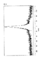
図1および2はN2下で5時間、ついで空気による、425℃の等温TGAを示す。これらの図は不活性(N2)雰囲気下でOSG型の材料より少し優れている。しかし、外界雰囲気を空気に代えると、劇的で急激な減量がOSG材料についてみられるが、本発明材料の膜は優れた安定性を示す。
【0061】
図3および4は425℃での等温後に、1000℃までの窒素もしくは空気中におけるTGA走査を示す。これらの図は、空気中で1000℃までの走査によるOSG(図4に示される)に対して、本発明の膜(例16、図3に示される)の熱安定性を示す。OSG材料は窒素中で10℃/分で走査されるとき、約400℃でのはるかに急速減量開始を示すのに対し、本発明の膜は、空気中で10℃/分で走査されるとき、約470℃でのみ開始し、長い時間にわたってはるかに少ない急速減量を示す。
【0062】
図5は空気中での425℃等温での、例16およびOSGの膜のIRプロフィルを示す。本発明の膜(点線プロフィル)がCO2と水のみを失うのに対し、OSG材料(実線プロフィル)は実質的に比較的大量のCO2ならびに水およびCH4を失うのをこの図は示す。試料から放出されるフッ素化有機材料(材料が所有すれば期待される)は何ら示されなかった。
【0063】
図6は例16の膜の13C−NMRスペクトルを示すが、有機フッ素の目にみえる徴候(−CH2Fについて約+90ppmから−CF3について約+150ppmまでの徴候を示すことが予測される)はみられない。この方法によりみられる炭素の唯一の形態は、ケイ素に結合された炭素であり、約0ppmを中心とする応答を示す。
【0064】
このように、本発明は膜およびこのような膜を製造するための方法を提供し、膜は実質的に、もしくは完全にC−F結合を含まず、OSG材料に対して低誘電率、ならびに改良された機械的性質、熱安定性、および耐薬品性(酸素、水性環境等に対する)を有する。
例21
オルガノシラン前駆体として1,3,5,7−テトラメチルシクロテトラシロキサンを用いることにもとづく本発明の見込みある例が、200mmシリコンウェハに関して下の表4に示される。
【0065】
【表4】
予測されるk値は2.8〜3.0の範囲にあり、ヤング率は約15GPa,そしてナノ押込み硬さは約2GPaである。
【0067】
オルガノシラン前駆体としてジメチルジメトキシシラン(DMDMOS)を用いることにもとづく本発明の見込みのある例は、200mmシリコンウェハに関して下の表5に示される。
【0068】
【表5】
予測されるk値は2.8〜3.0の範囲にあり、ヤング率は約15GPa,そしてナノ押込み硬さは約2GPaである。
【0070】
オルガノシラン前駆体としてジエトキシメチルシラン(DEMS)を用いることにもとづく本発明の見込みのある例は、200mmシリコンウェハに関して下の表6に示される。
【0071】
【表6】
予測されるk値は2.8〜3.0の範囲にあり、ヤング率は約15GPa,そしてナノ押込み硬さは約2GPaである。
【0073】
本発明はその特定の例について詳しく説明されたが、種々の変更および修正が本発明の精神および範囲を逸脱しないでなされうることは当業者に明らかであろう。
【図面の簡単な説明】
【図1】本発明の膜の1態様についての等温TGAを示す。
【図2】従来技術の膜についての等温TGAを示す。
【図3】本発明の膜の1態様についてのTGA走査を示す。
【図4】従来技術の膜についてのTGA走査を示す。
【図5】本発明の膜の1態様および従来技術の膜についてのIRプロフィルを示す。
【図6】本発明の膜の1態様についての13C−NMRスペクトルを示す。[0001]
BACKGROUND OF THE INVENTION
The present invention relates to a low dielectric constant material and a CVD processing method.
[0002]
[Prior art]
The electronics industry uses dielectric materials as insulating layers between circuits and integrated circuits and associated electronics devices. Line dimensions have been reduced to increase the speed and storage capability of microelectronic devices (eg, computer chips). Since microchip dimensions have experienced a significant reduction even over the past decade, the line width conventionally larger than 1 μm has been reduced to 0.18 μm, and future plans on drawing boards are at least It is as low as 0.07 μm. Delay time formula T = 1/2 RCL2(T is the delay time, R is the resistance of the conductive line, C is the capacitance of the insulating layer, and L is the wire length) is often used to define the effect of changing dimensions, and the material in the circuit Has signal propagation. Capacitance is C = k0k (S / d), where k0Is the vacuum permittivity or dielectric constant (equal to 1.0), k is the dielectric constant for the thin film, S is the electrode surface area, and d is the film thickness. Thus, a reduction in k results in a proportional reduction in C and thus a reduction in delay time. In addition, as line dimensions decrease, better insulating materials with relatively low dielectric constants need to prevent signal crossover (aka crosstalk) between chip components, which can negatively impact performance. .
[0003]
Historically, silica having a dielectric constant (k) of 4.2 to 4.5 has been used as an interlayer dielectric (ILD). However, at linear dimensions below 0.25 μm, silica can no longer be accepted and has been widely replaced by other materials, such as fluorinated silica glass (FSG), where k is about 3.6. Addition of fluorine to silica, which is specifically aimed at reducing the k value of undoped silica, has been studied in the past few years (see, for example, US Pat. Nos. 5,571,576, 5,661,093, 5, 700,736, 5,703,404, 5,827,785 and 5,872,065). The high electronegativity of fluorine gives rise to highly non-polarizable species and reduces the dielectric constant. Fluorinated silica is accepted by the industry and is used for the current generation of ICs.
[0004]
Since fluorinated silica materials have the thermal and mechanical stability necessary to withstand very high temperatures (up to 500 ° C.), the properties of the material (eg, low water absorption, mechanical properties) can be attributed to large amounts of fluorine. It is easy to be damaged when blended into. Despite having a very low k value up to 2.0 or less, fluorinated organic materials such as poly (tetrafluoroethylene) are sufficient for the temperatures encountered during the next processing step involved in integrated circuit fabrication. Stability was not exhibited. In general, organic polymers do not have sufficient mechanical strength for processing under current conditions, and in addition, fluorocarbon polymers have poor adhesion, potential reaction with metals at high temperatures, and in some cases at high temperatures. May have other disadvantages such as insufficient stiffness. Insulating films based on silica that incorporate both organic dopants and inorganic fluorine species to obtain desired property characteristics and low dielectric constant values have lower k values than FSG, and organosilica glass (OSG) materials Although it may have good thermal and mechanical properties, it maintains the necessary properties to act as an interlayer / intermetal material in IC manufacturing.
[0005]
More recently, OSG has been sought as an alternative to FSG. OSG materials are recommended as future interlayer / intermetal dielectrics of the type produced by CVD. A number of patents have been issued including the use of various organosilanes for the production of thin films having a k value of about 2.7 to 3.2 (see, for example, US Pat. No. 5,989,998, 6, 054,379, 6,072,227, 6,147,009 and 6,159,871 and WO 99/41423). OSG thin film insulation materials have been commercialized and advertised by several major OEMs for future ICs due to their inherently low k (<3.2) relative to FSG. However, the reduction in k must be harmonized against the detrimental effects that organic species typically have, including reduced mechanical properties, thermal stability and chemical resistance. Studies have shown that suitable material properties for OSG limit the dielectric constant to the range of 2.8 to 3.2, and the modulus / hardness value is in the range of 9 to 11 / 1.2 to 1.4 GPa. (See Lee et al., 198th Meeting of The Electronic Society, Oct. 2000, Section H-1, Abstract No. 531; and Golden et al., MICRO, page 31, February 2001).
[0006]
Some recent literature and patents have proposed the use of carbon-doped FSG materials. Most of these examples widely use fluorocarbon materials as precursors in combination with silicon precursor sources and introduce fluorocarbon moieties into the silica or FSG framework. For example, Shirafuji et al. Replaced hexamethyldisiloxane with octafluorobutene (Plasmas and Polymers, 4 (1) (57-75) March 1999) or tetrafluoroethylene (38 Jpn. J. Appl. Phys. 4520-26 ( 1999)) to produce a fluorocarbon / SiO composite film having an increased fluorocarbon content with k increased from 2.0 to 3.3. Yun et al. (341 (1,2) Thin Solid Films 109-111 (1999)) described triethoxyfluorosilane and O2The effect of adding fluorocarbon to the SiOF film produced in the helicon plasma reactor is examined.
[0007]
Another example of a specific mix of fluorocarbon moieties in silica is the work of Kim et al. 1998 IEEE International Conference On Conduction and Breakdown in Solid Directives 229-32 (1998), which essentially k from materials on silica. The ability to add a fluorocarbon for reduction will be described. Kim et al. Researched 2% silane / N2CF in plasmaFourAppears to be specifically aimed at introducing fluorocarbon moieties, producing films containing silicon, oxygen, carbon, fluorine, and N, where they are Si-C, Si-N, Si- O and C-F functionality could be observed. In addition, they found that the composition had a depth profile, according to which the surface was more oxygen than the bulk.
[0008]
U.S. Pat. No. 5,800,877 to Maeda et al. Describes a mixture of organosilane precursors having Si-F bonds and organosilane precursors having no Si-F bonds in a heat treatment for producing fluorine-containing silicon dioxide films. Is used with ozone or oxygen. The claims of this patent include the production of fluorine-containing silicon dioxide by a heat treatment with oxygen and / or nitrogen plasma post-treatment. This patent does not describe the introduction of alkyl groups or carbon into the membrane.
[0009]
In the paper by Hasegawa et al. (37 Jpn. J. Appl. Phys. 4904-09 (1998)), the increased water resistance of fluoride glass is observed in silane, oxygen and CF in a plasma enhanced CVD system.FourMotivation for deposition using a mixture of ammonia and ammonia. The deposited film was found to contain significant amounts of Si—N and C—F bonds by XPS spectral analysis. The improvement in water resistance due to the introduction of Si-N has a negative effect on the k value.
[0010]
In a similar study by the same group as described above, Lubbuban et al. (337 Thin Solid Films 67-70 (1999), 606 Materials Research Society Symposium Proceedings 57 (2000), and 87 (8) Journal of Apy 22 Ap. Considers the introduction of carbon into fluorosilicate glass by PE (plasma enhanced) -CVD to improve water resistance. The material was synthesized from silane or TEOS, oxygen, methane and perfluoromethane and investigated for composition, thermal stability, and electrical properties. Lububan et al., SiO2We propose that the introduction of both carbon and fluorine into the network reduces the dielectric constant. The increase in the amount of methane introduced into the deposition chamber during the reaction results in an increase in the carbon and fluorine of the final material, which is said to be caused by a significant contribution from the C—F functionality. As described in their paper, the presence of C—F and C—H species promotes water absorption resistance and helps reduce the dielectric constant.
[0011]
In a Japanese patent by Fujitsu Ltd. (Japanese Patent Laid-Open No. 10-150036), an organosilicon material deposited by spin coating increases heat resistance, reduces water absorption by the formation of fluorocarbon species in the film, and F in a plasma reactor to increase the material reliability of the membrane2Or NFThreeAfter-deposition treatment by. Other Fujitsu Ltd. patents (Japanese Patent Laid-Open Nos. 58-21499 and 11-1111712) also show silica having fluorocarbon species compounded by plasma CVD using a silicon-based precursor containing a fluorocarbon group. Consider film formation.
[0012]
Uchida et al. Disclose a fluorinated organosilica membrane for improved moisture resistance. For example, 98 (3) Electrochem. Soc. 163-8 (1998), 37 Jpn. J. et al. Appl. Phys. 6369-73 (1998), 38 Jpn. J. et al. Appl. Phys. 2368-72 (1999) and JP-A-11-111714. In these articles, etc., the authors point out that FSG and OSG properties can be complementary so that materials with both functionalities can take advantage of their strength, but little supportive data is shown. . The authors use tert-methylamine (TMA), tetraisocyanate-silane (TICS), dimethyl diisocyanate-silane (DMSIC) and preferably dimethyl to produce silica films in which the organosilicon material is free of H and OH. We attempt to demonstrate this expressed advantage by describing a process deposited by heat treatment from a mixture of ethylamine (DMA). This deposited film was post-treated with HF in a heat treatment to replace the isocyanate species with fluorine, and a film with a lower dielectric constant and better moisture resistance was produced. However, the resulting film contained C-Si and C-F functionality. In addition, a compositional gradient caused by the film depth was produced, as is common in diffusion based processes such as chemical post treatment. It is inherently difficult to control the amount and uniformity of chemical modification of the membrane in this manner.
[0013]
Usami US Pat. No. 6,077,574 discloses a method for producing plasma CVD silicon oxide insulating films doped with specific amounts of fluorine and carbon, wherein the films are independent of fluorine concentration and carbon concentration. It is deposited from a feed gas mixture which can be adjusted in a controlled manner. The atomic ratio ([carbon] / [fluorine]) in these films is 4.0 × 10twenty oneFluorine atoms / cc to 1.0 × 10twenty twoFluorine atom / cc, and 3.0 × 10¹⁹Carbon atoms / cc to 1.0 × 10twenty one0.25 or less based on the disclosed concentration range of carbon atoms / cc. No data is given regarding the functionality produced in the membrane. 6.6 × 10twenty twoGiven a density of about 2.2 g / cc of silica equal to atoms / cc, the concentration of fluorine and carbon is estimated to be about 6-15 atomic% fluorine, and about 0.05-1.5 atomic% carbon. sell.
[0014]
Despite the foregoing developments, there has been no prior art example that successfully combines the desired mechanical, dielectric, thermal and oxidative stability that is superior for integrating low-k insulating materials in integrated circuits. .
[0015]
All references cited herein are hereby incorporated by reference in their entirety.
[0016]
[Problems to be solved by the invention]
It is an object of the present invention to provide a thin film material having a low dielectric constant and improved mechanical properties, thermal stability and chemical resistance.
[0017]
[Means for Solving the Problems]
The present invention provides a film of carbon-doped fluorosilicate glass (ie, CFSG or OFSG-organofluorosilicate glass) that contains both organic species and inorganic fluorine, with the exception of significant amounts of fluorocarbon species.
[0018]
More specifically, preferred films of the present invention are of formula SivOwCxHyFz(V + w + x + y + z = 100%, v is 10-35 atomic%, w is 10-65 atomic%, y is 10-50 atomic%, x is 2-30 atomic%, and z is 0.1-15 atomic%) And substantially fluorine is represented without being bound to carbon.
[0019]
Furthermore, the formula SivOwCxHyFz(V + w + x + y + z = 100%, v is 10-35 atomic%, w is 10-65 atomic%, y is 10-50 atomic%, x is 1-30 atomic%, and z is 0.1-15 atomic%) A film is provided wherein x / z> 0.25 and substantially no fluorine is bonded to the carbon.
[0020]
The present invention further provides a chemical vapor deposition method for producing such films,
a. Providing a substrate in a vacuum chamber;
b. Introducing a gaseous reagent comprising a gas supplying fluorine, a gas supplying oxygen, and a gaseous reagent comprising at least one precursor gas selected from the group consisting of organosilane and organosiloxane; and
c. Applying energy to the gaseous reagent in the chamber to cause a reaction of the gaseous reagent and to form a film on the substrate;
including.
[0021]
And further providing an improved method for producing organosilica glass by chemical vapor deposition of organosilane, the improvement co-depositing inorganic fluorine with at least one part of organosilane from an inorganic fluorine source. Including.
[0022]
DETAILED DESCRIPTION OF THE INVENTION
Preferred embodiments of the present invention provide thin film materials that have a low dielectric constant and improved mechanical properties, thermal stability and chemical resistance (oxygen, aqueous environment, etc.) for OSG materials. This does not produce significant amounts of organic fluorine (eg, C—F bonds) and is carbon (which can be silicon carbide, but is preferably primarily organic carbon —CHx(X is in the form of 1 to 3) and the result of introduction of inorganic fluorine (for example, Si-F bond) into the film. Thus, the final thin film material preferably includes Si—O, Si—F, C—H and Si—C bond structures, and substantially and more preferably entirely includes C—F bonds. And preferably most of the hydrogen is bonded to carbon. Other relatively less functional parts such as Si-H, C-O and OH may also be present in certain films of the present invention.
[0023]
Thus, preferred embodiments of the present invention are: (a) about 10 to about 35 atomic percent, more preferably about 20 to about 30 atomic percent silicon; (b) about 10 to about 65 atomic percent, more preferably About 20 to about 40 atomic percent oxygen; (c) about 10 to about 50 atomic percent, more preferably about 20 to about 40 atomic percent hydrogen; (d) about 1 to about 30 atomic percent, more preferably about 5 To about 25 atomic percent carbon; and (e) about 0.1 to about 15 atomic percent, more preferably about 0.5 to about 7.0 atomic percent fluorine. A relatively small portion of other elements may also be present in certain films of the present invention.
[0024]
Both FSG and OSG materials are considered low-k materials because their dielectric constant is lower than the standard material traditionally used in the industry-silica glass. The combination of both inorganic fluorine and organic carbon dope into the film has a linking effect on the final material k. This is obvious in a different way. For example, the film may have significant mechanical properties such as OSG material but have a relatively low k, or may have significant k but excellent mechanical properties. The introduction of methyl groups into the silica membrane can give the membrane nanoporosity and help reduce the k of the membrane, but can also reduce the mechanical properties of the membrane. The films of the present invention preferably contain from about 1 to about 30 atomic percent or from about 2 to about 30 atomic percent of carbon, with most of the hydrogen bonded to the carbon. Suitably part of the CH functionality is in the methyl group. In general, the introduction of porosity is an effective way to reduce the dielectric constant of a material. The addition of porosity affects the mechanical and heat transfer properties (eg, extensive properties) of the membrane, but does not change the inherent chemical or thermal stability of the membrane. Some embodiments of the membrane are nanoporous with respect to silica. Silica produced by PE-CVD TEOS has an intrinsic free volume pore size of about 0.6 nm as measured by positron annihilation lifetime spectroscopy (PALS) analysis. The pore diameter of the present invention measured by small angle neutron scattering (SANS) or PALS is preferably an equivalent sphere diameter of less than 5 nm, more preferably an equivalent sphere diameter of less than 2.5 nm.
[0025]
Preferably, the membrane of the present invention has a density of less than 2.0 g / cc, alternatively less than 1.5 g / cc. Such low density can be achieved by adding a porogen to the gaseous reagent and / or by post-treating the deposited material.
[0026]
The films of the present invention have improved properties with respect to OSG materials. A given OFSG has better mechanical properties than an equivalent stoichiometric OSG material, but lacks fluorine in the OSG material. For example, a preferred embodiment of the OFSG material of the present invention has a dielectric constant of less than 3.5, more preferably less than 3.0. In certain embodiments, the film has a dielectric constant in the range of 2.8 to 3.2, an elastic modulus greater than 10 GPa, and / or a nanoindentation hardness greater than 1.5 GPa.
[0027]
The membrane of the present invention is thermally stable and has good chemical resistance. In particular, the membrane is N2Having an average weight loss of less than 1.0 wt% / hr at an isothermal temperature of 425 ° C. and / or an average weight loss of less than 1.0 wt% / hr at an isothermal temperature of 425 ° C. in air.
[0028]
The membrane is suitable for various applications. In particular, the film is suitable for deposition on a semiconductor substrate and, for example, in integrated circuits, insulating layers, interlayer insulating films, intermetallic insulating films, capping layers, chemical mechanical planarization (CMP) or etching stop layers, barrier layers Particularly suitable for use as an adhesive layer (for example against unwanted metal, water or other material diffusion in the insulating layer). The membrane can form a compatible coating. The mechanical properties exhibited by these films make them particularly compatible for use in Al subtractive and Cu damascene methods.
[0029]
The film is compatible with chemical mechanical planarization and anisotropic etching, and silicon, SiO2, SiThreeNFour, OSG, FSG, silicon carbide, antireflective coatings, photoresists, organic polymers, porous organic and inorganic materials, metals such as copper and aluminum, and various materials such as metal barrier layers.
[0030]
The invention is particularly suitable for supplying membranes, and the products of the invention are mainly described herein as membranes, but the invention is not limited thereto. The products of the present invention can be supplied in any form that can be deposited by CVD, such as coatings, multilayer assemblies, and other types of objects that are not necessarily flat or thin, and many objects that are not necessarily used in integrated circuits. obtain.
[0031]
In addition to the product of the present invention, the present invention includes methods by which the product is produced, as well as methods of using the product.
[0032]
In some embodiments, the invention includes an improved method for depositing OSG by chemical vapor deposition, wherein the inorganic fluorine source is at least a portion of the OSG material for producing a film substantially free of organic fluorine. Inorganic fluorine is deposited during the deposition. Thus, the present invention can be used to improve conventional, modern and future methods, such as US Pat. Nos. 6,054,379, 6,147,009 and 6,159,871 and WO99 / 871. 41423 is included. Products produced by the improved process enjoy improved properties with respect to products produced by conventional processes. Preferably, the at least one mechanical property of the membrane is increased by at least 10%, the thermal stability of the membrane is increased, the chemical stability of the membrane is increased, and / or the environmental stability of the membrane is increased. .
[0033]
The method for obtaining a film with a low induction rate is:
(A). Providing a substrate in a vacuum chamber;
(B). Introducing a gaseous reagent comprising a gas supplying fluorine, a gas supplying oxygen, and at least one precursor gas selected from the group consisting of organosilanes and organosiloxanes into a vacuum chamber; and
c. Applying energy to the gaseous reagent in the chamber to cause a reaction of the gaseous reagent and to form a film on the substrate;
Including stages.
[0034]
Preferably the substrate is a semiconductor.
[0035]
Organosilanes and organosiloxanes are suitable precursor gases. Suitable organosilanes and organosiloxanes are, for example: (a) the general formula R1 nSiR2 4-nWhere n is an integer from 1 to 3;1And R2Are independently at least one branched or straight chain C1~ C8Alkyl group (for example, methyl, ethyl), CThree~ C8Substituted or unsubstituted cycloalkyl group, C2~ CTenA partially substituted alkyl group of (for example, propenyl, butadienyl), C6~ C12A corresponding linear, branched, cyclic, partially unsubstituted alkyl, or aromatic containing a substituted or unsubstituted aromatic (eg, phenyl, tolyl), an alkoxy group (eg, methoxy, ethoxy, phenoxy), and / or R2Is a hydride (for example, methylsilane, dimethylsilane, trimethylsilane, tetramethylsilane, phenylsilane, methylphenylsilane, cyclohexylsilane, tert-butylsilane, ethylsilane, diethylsilane, tetraethoxysilane, dimethylciethoxysilane, dimethyl Dimethoxysilane, dimethylethoxysilane, methyldiethoxysilane, triethoxysilane, trimethylphenoxysilane and phenoxysilane); (b) formula R1(R2 2SiO)nSiR2 ThreeA linear organosilane represented by the formula (n is an integer of 1 to 10) or the formula (R1R2SiO)n(Wherein n is an integer of 2 to 10) (where R1And R2(For example, 1,3,5,7-tetramethylcyclotetrasiloxane, octamethylcyclotetrasiloxane, hexamethylcyclotrisiloxane, hexamethyldisiloxane, 1,1,2,2-tetramethyl) Disiloxane and octamethyltrisiloxane); and (c) Formula R2(SiR1R2)nR2A linear organosilane oligomer represented by the formula (n is an integer of 2 to 10), or a formula (SiR1R2)n(Where n is an integer of 3 to 10) (where R1And R2Is as described above) (for example, 1,2-dimethyldisilane, 1,1,2,2-tetramethyldisilane, 1,2-dimethyl-1,1,2,2-dimethoxydisilane, hexamethyldisilane, Octamethyltrisilane, 1,2,3,4,5,6-hexaphenylhexasilane, 1,2-dimethyl-1,2-diphenyldisilane and 1,2-diphenyldisilane).
[0036]
In some embodiments, the organosilane / organosiloxane is a cyclic alkyl silane, a cyclic alkoxy silane, or contains at least one alkoxy or alkyl bridge between a pair of Si atoms, such as 1,2-disilanoethane, 1,3- Disilanopropane, dimethyldisilacyclobutane, 1,2-bis (trimethylsiloxy) cyclobutene, 1,1-dimethyl-1, -sila-2,6-dioxacyclohexane, 1,1-dimethyl-1-sila-2 -Oxacyclohexane, 1,2-bis (trimethylsiloxy) ethane, 1,4-bis (dimethylsilyl) benzene or 1,3- (dimethylsilyl) cyclobutane.
[0037]
In some embodiments, the organosilane / organosiloxane comprises an epoxide, carboxylate, alkyne, diene, phenylethynyl, distorted cyclic group, and trimethylsilacetylene, 1- (trimethylsilyl) -1,3-butadiene, trimethylsilylcyclopentadiene, C that can sterically hinder or distort organosilanes / organosiloxanes such as trimethylsilylacetate and di-tert-butoxydiacetoxysilaneFour~ CTenA reactive side group selected from the group consisting of:
[0038]
A suitable fluorine supplying gas lacks any F—C bonds (ie, fluorine bonded to carbon) that terminate in the membrane. Such a suitable gas for supplying fluorine is, for example, SiF.Four, NFThree, F2, HF, SF6, ClFThree, BFThree, BrFThree, SFFour, NF2Cl, FSiHThree, F2SiH2, FThreeIncluding SiH, organofluorosilane and mixtures thereof, the organofluorosilane does not contain any FC bonds. In addition, suitable fluorine supplying gases include the alkyl silanes, alkoxy silanes, linear and cyclic organosiloxanes described above, linear and cyclic organosilane oligomers, cyclic and crosslinked organosilanes, and organosilanes having reflective side groups. , Since the fluorine atom is substituted with at least one of the silicon substituents, there is at least one Si-F bond. More particularly, suitable fluorine supplying gases include, for example, fluorotrimethylsilane, difluorodimethylsilane, methyltrifluorosilane, fluorotriethoxysilane, 1,2-difluoro-1,1,2,2-tetramethyldisilane. Alternatively, difluorodimethoxysilane is included.
[0039]
A suitable oxygen supplying gas is, for example, O2, N2O, ozone, hydrogen peroxide, NO, NO2, N2OFourOr a mixture thereof.
[0040]
It is within the scope of the present invention for a single species of molecule to act as one or more of a precursor gas, a gas supplying oxygen, and a gas supplying fluorine. That is, the precursor gas, the oxygen supplying gas, and the fluorine supplying gas are not necessarily three different gases. For example, it is possible to use dimethoxymethylfluorosilane to provide silicon, carbon, oxygen and fluorine. In addition, a precursor gas and a gas that supplies oxygen (eg, tetraethoxysilane, trimethylsilylacetate, or dimethoxydimethylsilane, each providing carbon, oxygen, and silicon) are used in a single gas, and the precursor It is also possible to use a single gas or the like that acts as a gas and a gas that supplies fluorine (for example, trimethylfluorosilane that provides carbon, fluorine, and silicon). In either case, it is preferred to avoid the use of reagents containing C—F functionality.
[0041]
The term “gaseous reagent” may be used herein to describe a reagent, but the term is supplied directly to the reactor as a gas, supplied as a vaporized liquid, as a sublimated solid, and And / or reagents transported to the reactor by an inert carrier gas.
[0042]
In some embodiments, a mixture of different organosilanes and / or organosiloxanes are used together. In addition, a number of different fluorine-providing gas combinations and / or a number of different oxygen-providing agent combinations may be used with or in combination with different organosilanes and / or organosiloxane combinations. Are also within the scope of the present invention. Moreover, it is within the scope of the present invention to use a fluorinated organosilane (to provide fluorine and / or carbon) with a non-fluorinated organosilane (to provide carbon).
[0043]
In addition to the fluorine supplying gas, the oxygen supplying gas, and the organosilane / organosiloxane, additional materials may be charged into the vacuum chamber before, during, and / or after the deposition reaction. Such materials include, for example, an inert gas (eg, He, Ar, N2, Kr, Xe, etc., which may be required as a carrier gas for relatively volatile precursors and / or promote annealing of the as-deposited material, resulting in a more stable final As well as gaseous or liquid organic substances, NHThree, H2, CO2Alternatively, it contains a reactive substance such as CO. For example, CHFour, C2H6, C2HFour, C2H2, CThreeH8Organic substances such as benzene, naphthalene, toluene and styrene are mixed in the film of the present invention to give carbon.
[0044]
Energy is applied to the gaseous reagent to react the gas and form a film on the substrate. Such energy can be supplied by, for example, heat, plasma, pulsed plasma, helicon plasma, high density plasma, inductively coupled plasma, and remote plasma methods. A secondary rf frequency source can be used to modify the plasma properties at the substrate surface. Preferably, the film is formed by plasma enhanced chemical vapor deposition. It is particularly preferred to generate a capacitively coupled plasma at a frequency of 13.56 MHz. The power of the plasma is preferably 0.02-7 W / cm based on the surface area of the substrate.2More preferably, 0.3 to 3 W / cm2It is.
[0045]
Each flow rate of the gaseous reagent is preferably 10 to 5000 sccm, more preferably 200 to 2000 sccm, for a single 200 mm wafer. Individual flow rates are selected to provide the desired amount and ratio of fluorine, carbon, etc. in the membrane. The actual flow rate required may depend on the wafer size and chamber configuration and is not limited to 200 mm wafers or single wafer chambers.
[0046]
It is preferred to deposit the film at a deposition rate of at least 50 nm / min. The pressure in the vacuum chamber during deposition is preferably 0.01 to 600 torr, more preferably 1 to 10 torr.
[0047]
A preferred formulation of the present invention based on using trimethylsilane as the organosilane precursor is shown in Table 1 below for a 200 mm silicon wafer substrate.
[0048]
[Table 1]
The method of the present invention is preferably accomplished in a single process step at a high flow rate. Although not wishing to be bound by any theory, the method of the present invention has a more uniform distribution of inorganic fluorine across the entire cross section of the membrane, unlike the multi-step post-treatment fluorination method as taught by Uchida et al. Providing a membrane. In addition, the insignificant amount of organic fluorine present in the films of the present invention (here “insubstantial”) is less than 5% total fluorine content, more preferably total fluorine content. Less than 1% (defined for this purpose) is also distributed relatively uniformly over the entire cross-section of the membrane and is not centered.
[0050]
In many cases, a single processing step is preferred, but it is also within the scope of the invention to post-process the film after deposition. Such post-treatment can include, for example, at least one of heat treatment, plasma treatment, and chemical treatment.
[0051]
The film is preferably deposited to a thickness of 0.002 to 10 μm, although the thickness can be varied as required. Blanket films deposited on non-patterned surfaces have excellent uniformity and less than 2% thickness variation over 1 standard deviation for substrates with moderate peripheral exclusion. Here, for example, the outermost periphery of 10 mm of the substrate is not included in the uniform statistical calculation.
[0052]
The porosity of the membrane can be increased with the bulk density, correspondingly decreasing to further reduce the dielectric constant of the material, and expand the applicability of this material to the next generation (eg, k <2.5).
[0053]
【Example】
The present invention is further illustrated by the following examples, but it should be understood that the present invention is not limited thereto.
Examples 1-20
All experiments were performed with an Applied Materials Precision-5000 system in a 200 mm DxZ chamber fitted with an AdvanceEnergy 2000rf generator using an undoped TEOS process kit. The recipe included the following basic steps: initial set-up and stabilization for chamber purge / evacuation prior to gas flow, deposition, and wafer removal. Next, the cleaning of the chamber2F6+ O2Was performed after each deposition, followed by the seasoning of the chamber.
[0054]
The dielectric constant was measured using a Hg probe method on a low resistivity P-type wafer, the mechanical properties were measured using an MTS Nano Indenter, and the thermal stability and off-gas products were measured using a MIDAC infrared spectrometer (TGA- IR) and was measured by thermogravimetric analysis using a Thermo TA Instruments 2050 TGA.13C-NMR data was obtained by Bruker ASX-200, and composition data was obtained by X-ray photoelectron spectroscopy (XPS) using Physical Electronics 5000LS.
[0055]
Comparative Examples 1-6 are performed according to US Pat. Nos. 6,159,871 and 6,054,379, and WO 99/41123, and are listed in Table 2 below.
[0056]
[Table 2]
The physical considerations for several different membranes produced by the present invention are listed in Table 3 below (Note: atomic% of hydrogen is not measured by XPS for Table 3).
[0058]
[Table 3]
Thickness and refractive index were measured on a
[0060]
1 and 2 are N2Shown is an isothermal TGA of 425 ° C. with 5 hours below and then with air. These figures are inactive (N2) A little better than OSG type material in atmosphere. However, when the ambient atmosphere is replaced with air, dramatic and rapid weight loss is seen for OSG materials, but the films of the present material exhibit excellent stability.
[0061]
Figures 3 and 4 show TGA scans in nitrogen or air up to 1000 ° C after isothermal at 425 ° C. These figures show the thermal stability of the inventive membrane (Example 16, shown in FIG. 3) versus OSG (shown in FIG. 4) by scanning up to 1000 ° C. in air. The OSG material shows a much faster onset of weight loss at about 400 ° C. when scanned at 10 ° C./min in nitrogen, whereas the membrane of the present invention is scanned at 10 ° C./min in air. Starting only at about 470 ° C., showing much less rapid weight loss over a longer period of time.
[0062]
FIG. 5 shows the IR profile of the film of Example 16 and OSG at 425 ° C. isothermal in air. The membrane of the present invention (dotted line profile) is CO2OSG material (solid line profile) has a relatively large amount of CO, whereas2And water and CHFourThis figure shows losing. No fluorinated organic material (expected if the material possesses) released from the sample was shown.
[0063]
FIG. 6 shows the membrane of Example 1613Shows C-NMR spectrum, but visible signs of organic fluorine (-CH2About +90 ppm to -CF for FThreeAre expected to show signs up to about +150 ppm). The only form of carbon found by this method is silicon bonded carbon, which shows a response centered around 0 ppm.
[0064]
Thus, the present invention provides films and methods for making such films, wherein the films are substantially or completely free of C—F bonds, have a low dielectric constant relative to OSG materials, and Has improved mechanical properties, thermal stability, and chemical resistance (against oxygen, aqueous environments, etc.).
Example 21
A promising example of the present invention based on using 1,3,5,7-tetramethylcyclotetrasiloxane as the organosilane precursor is shown in Table 4 below for a 200 mm silicon wafer.
[0065]
[Table 4]
The predicted k value is in the range of 2.8 to 3.0, the Young's modulus is about 15 GPa, and the nanoindentation hardness is about 2 GPa.
[0067]
A promising example of the present invention based on using dimethyldimethoxysilane (DMDMOS) as the organosilane precursor is shown in Table 5 below for a 200 mm silicon wafer.
[0068]
[Table 5]
The predicted k value is in the range of 2.8 to 3.0, the Young's modulus is about 15 GPa, and the nanoindentation hardness is about 2 GPa.
[0070]
A promising example of the present invention based on using diethoxymethylsilane (DEMS) as the organosilane precursor is shown in Table 6 below for a 200 mm silicon wafer.
[0071]
[Table 6]
The predicted k value is in the range of 2.8 to 3.0, the Young's modulus is about 15 GPa, and the nanoindentation hardness is about 2 GPa.
[0073]
Although the invention has been described in detail with respect to specific examples thereof, it will be apparent to those skilled in the art that various changes and modifications can be made without departing from the spirit and scope of the invention.
[Brief description of the drawings]
FIG. 1 shows isothermal TGA for one embodiment of the membrane of the present invention.
FIG. 2 shows isothermal TGA for prior art membranes.
FIG. 3 shows a TGA scan for one embodiment of the membrane of the present invention.
FIG. 4 shows a TGA scan for a prior art film.
FIG. 5 shows an IR profile for one embodiment of the membrane of the present invention and a prior art membrane.
FIG. 6 shows one embodiment of the membrane of the present invention.13A C-NMR spectrum is shown.
Claims (39)
a.真空チャンバ内に基板を用意すること;
b.フッ素を供給するガス、酸素を供給するガス、ならびにオルガノシランおよびオルガノシロキサンからなる群より選ばれる少なくとも1つの前駆体ガスを含むガス状試薬を真空チャンバに導入すること;ならびに
c.該チャンバ内のガス状試薬にエネルギーを加えてガス状試薬の反応を引き起こさせ、そして基板上に膜を形成させること、
を含む方法。A chemical vapor deposition method for producing the film of claim 1, the method comprising:
a. Providing a substrate in a vacuum chamber;
b. Introducing a gaseous reagent comprising a gas supplying fluorine, a gas supplying oxygen, and at least one precursor gas selected from the group consisting of an organosilane and an organosiloxane into a vacuum chamber; and c. Applying energy to the gaseous reagent in the chamber to cause a reaction of the gaseous reagent and to form a film on the substrate;
Including methods.
(ここでR1およびR2は独立して、少なくとも1つの分枝もしくは直鎖C1〜C8のアルキル基、C3〜C8の置換もしくは非置換シクロアルキル基、C2〜C10の部分置換アルキル基、C6〜C12の置換もしくは非置換芳香族、アルコキシ基を含有する対応する線状、分枝、環状、部分非置換アルキル、もしくは芳香族、ならびにあるいはR2は水素化物である)
である請求項16記載の方法。At least one precursor has the formula I: R 1 a linear organosiloxane of the (R 2 2 SiO) n SiR 2 3 (n is an integer of 1 to 10) or formula II: (R 1 R 2 SiO ) n of cyclic organosiloxanes (n is an integer of 2 to 10)
Wherein R 1 and R 2 are independently at least one branched or straight chain C 1 -C 8 alkyl group, C 3 -C 8 substituted or unsubstituted cycloalkyl group, C 2 -C 10 A partially substituted alkyl group, a C 6 -C 12 substituted or unsubstituted aromatic, the corresponding linear, branched, cyclic, partially unsubstituted alkyl or aromatic containing an alkoxy group, and / or R 2 is a hydride is there)
The method according to claim 16.
(ここでR1およびR2は独立して、少なくとも1つの分枝もしくは直鎖C1〜C8のアルキル基、C3〜C8置換もしくは非置換シクロアルキル基、C2〜C10の部分置換アリキル基、C6〜C12の置換もしくは非置換芳香族、アルコキシ基を含有する対応する線状、分枝、環状、部分非置換アルキル、もしくは芳香族、ならびにあるいはR2は水素化物である)
である請求項16記載の方法。At least one precursor is a linear organosilane oligomer of the general formula R 2 (SiR 1 R 2 ) n R 2 (n is an integer of 2 to 10), or a cyclic organo of the general formula (SiR 1 R 2 ) n Silane oligomer (n is an integer of 3 to 10)
Wherein R 1 and R 2 are independently at least one branched or straight chain C 1 -C 8 alkyl group, a C 3 -C 8 substituted or unsubstituted cycloalkyl group, a C 2 -C 10 moiety. substituted Arikiru group, a substituted or unsubstituted aromatic C 6 -C 12, corresponding linear containing alkoxy group, branched, cyclic, partially unsubstituted alkyl or aromatic, and or R 2 is a hydride )
The method according to claim 16.
Applications Claiming Priority (2)
| Application Number | Priority Date | Filing Date | Title |
|---|---|---|---|
| US09/863,150 US6716770B2 (en) | 2001-05-23 | 2001-05-23 | Low dielectric constant material and method of processing by CVD |
| US09/863150 | 2001-05-23 |
Related Child Applications (1)
| Application Number | Title | Priority Date | Filing Date |
|---|---|---|---|
| JP2004200926A Division JP2004312041A (en) | 2001-05-23 | 2004-07-07 | Low-dielectric constant material and treatment method by cvd |
Publications (2)
| Publication Number | Publication Date |
|---|---|
| JP2003007699A JP2003007699A (en) | 2003-01-10 |
| JP3881282B2 true JP3881282B2 (en) | 2007-02-14 |
Family
ID=25340388
Family Applications (2)
| Application Number | Title | Priority Date | Filing Date |
|---|---|---|---|
| JP2002149738A Expired - Fee Related JP3881282B2 (en) | 2001-05-23 | 2002-05-23 | Low dielectric constant material and CVD processing method |
| JP2004200926A Withdrawn JP2004312041A (en) | 2001-05-23 | 2004-07-07 | Low-dielectric constant material and treatment method by cvd |
Family Applications After (1)
| Application Number | Title | Priority Date | Filing Date |
|---|---|---|---|
| JP2004200926A Withdrawn JP2004312041A (en) | 2001-05-23 | 2004-07-07 | Low-dielectric constant material and treatment method by cvd |
Country Status (7)
| Country | Link |
|---|---|
| US (1) | US6716770B2 (en) |
| EP (1) | EP1260606A3 (en) |
| JP (2) | JP3881282B2 (en) |
| KR (1) | KR100489758B1 (en) |
| CN (1) | CN1255573C (en) |
| SG (1) | SG111942A1 (en) |
| TW (1) | TW574410B (en) |
Families Citing this family (124)
| Publication number | Priority date | Publication date | Assignee | Title |
|---|---|---|---|---|
| US5989998A (en) * | 1996-08-29 | 1999-11-23 | Matsushita Electric Industrial Co., Ltd. | Method of forming interlayer insulating film |
| US6660656B2 (en) | 1998-02-11 | 2003-12-09 | Applied Materials Inc. | Plasma processes for depositing low dielectric constant films |
| US6800571B2 (en) * | 1998-09-29 | 2004-10-05 | Applied Materials Inc. | CVD plasma assisted low dielectric constant films |
| US6777171B2 (en) | 2001-04-20 | 2004-08-17 | Applied Materials, Inc. | Fluorine-containing layers for damascene structures |
| US7074489B2 (en) * | 2001-05-23 | 2006-07-11 | Air Products And Chemicals, Inc. | Low dielectric constant material and method of processing by CVD |
| DE10131156A1 (en) * | 2001-06-29 | 2003-01-16 | Fraunhofer Ges Forschung | Articles with a plasma polymer coating and process for its production |
| JP3749162B2 (en) * | 2001-12-05 | 2006-02-22 | キヤノン販売株式会社 | Manufacturing method of semiconductor device |
| US20030224544A1 (en) * | 2001-12-06 | 2003-12-04 | Shipley Company, L.L.C. | Test method |
| US20030194496A1 (en) * | 2002-04-11 | 2003-10-16 | Applied Materials, Inc. | Methods for depositing dielectric material |
| US6815373B2 (en) * | 2002-04-16 | 2004-11-09 | Applied Materials Inc. | Use of cyclic siloxanes for hardness improvement of low k dielectric films |
| US8951342B2 (en) | 2002-04-17 | 2015-02-10 | Air Products And Chemicals, Inc. | Methods for using porogens for low k porous organosilica glass films |
| US7384471B2 (en) * | 2002-04-17 | 2008-06-10 | Air Products And Chemicals, Inc. | Porogens, porogenated precursors and methods for using the same to provide porous organosilica glass films with low dielectric constants |
| US9061317B2 (en) | 2002-04-17 | 2015-06-23 | Air Products And Chemicals, Inc. | Porogens, porogenated precursors and methods for using the same to provide porous organosilica glass films with low dielectric constants |
| US8293001B2 (en) * | 2002-04-17 | 2012-10-23 | Air Products And Chemicals, Inc. | Porogens, porogenated precursors and methods for using the same to provide porous organosilica glass films with low dielectric constants |
| US20080268177A1 (en) * | 2002-05-17 | 2008-10-30 | Air Products And Chemicals, Inc. | Porogens, Porogenated Precursors and Methods for Using the Same to Provide Porous Organosilica Glass Films with Low Dielectric Constants |
| US6936551B2 (en) * | 2002-05-08 | 2005-08-30 | Applied Materials Inc. | Methods and apparatus for E-beam treatment used to fabricate integrated circuit devices |
| US7060330B2 (en) * | 2002-05-08 | 2006-06-13 | Applied Materials, Inc. | Method for forming ultra low k films using electron beam |
| JP4217870B2 (en) * | 2002-07-15 | 2009-02-04 | 日本電気株式会社 | Organosiloxane copolymer film, manufacturing method thereof, growth apparatus, and semiconductor device using the copolymer film |
| US6878641B2 (en) * | 2002-10-01 | 2005-04-12 | Advanced Technology Materials, Inc. | Composition and chemical vapor deposition method for forming organic low k dielectric films |
| US20040166692A1 (en) * | 2003-02-26 | 2004-08-26 | Loboda Mark Jon | Method for producing hydrogenated silicon oxycarbide films |
| TWI240959B (en) * | 2003-03-04 | 2005-10-01 | Air Prod & Chem | Mechanical enhancement of dense and porous organosilicate materials by UV exposure |
| US20050260420A1 (en) * | 2003-04-01 | 2005-11-24 | Collins Martha J | Low dielectric materials and methods for making same |
| US8137764B2 (en) * | 2003-05-29 | 2012-03-20 | Air Products And Chemicals, Inc. | Mechanical enhancer additives for low dielectric films |
| US6967405B1 (en) * | 2003-09-24 | 2005-11-22 | Yongsik Yu | Film for copper diffusion barrier |
| US20050074554A1 (en) * | 2003-10-06 | 2005-04-07 | Shiu-Ko Jangjian | Method of forming inter-metal dielectric layer structure |
| WO2005053009A1 (en) * | 2003-11-28 | 2005-06-09 | Nec Corporation | Porous insulating film, method for producing same, and semiconductor device using porous insulating film |
| KR101021178B1 (en) * | 2003-12-24 | 2011-03-15 | 매그나칩 반도체 유한회사 | Dieletric layer in a semiconductor device and method of forming the same |
| DE102004008442A1 (en) * | 2004-02-19 | 2005-09-15 | Degussa Ag | Silicon compounds for the production of SIO2-containing insulating layers on chips |
| US7049247B2 (en) * | 2004-05-03 | 2006-05-23 | International Business Machines Corporation | Method for fabricating an ultralow dielectric constant material as an intralevel or interlevel dielectric in a semiconductor device and electronic device made |
| US7282438B1 (en) | 2004-06-15 | 2007-10-16 | Novellus Systems, Inc. | Low-k SiC copper diffusion barrier films |
| JP2006024670A (en) * | 2004-07-07 | 2006-01-26 | Sony Corp | Manufacturing method for semiconductor device |
| US7288205B2 (en) * | 2004-07-09 | 2007-10-30 | Applied Materials, Inc. | Hermetic low dielectric constant layer for barrier applications |
| US7581549B2 (en) * | 2004-07-23 | 2009-09-01 | Air Products And Chemicals, Inc. | Method for removing carbon-containing residues from a substrate |
| US7357977B2 (en) * | 2005-01-13 | 2008-04-15 | International Business Machines Corporation | Ultralow dielectric constant layer with controlled biaxial stress |
| US7291563B2 (en) * | 2005-08-18 | 2007-11-06 | Micron Technology, Inc. | Method of etching a substrate; method of forming a feature on a substrate; and method of depositing a layer comprising silicon, carbon, and fluorine onto a semiconductor substrate |
| US20070077778A1 (en) * | 2005-10-04 | 2007-04-05 | The Boc Group, Inc. | Method of forming low dielectric constant layer |
| CN100539071C (en) * | 2006-02-16 | 2009-09-09 | 中芯国际集成电路制造(上海)有限公司 | Be used to form the method for low dielectric constant fluorine doping layer |
| US7902080B2 (en) * | 2006-05-30 | 2011-03-08 | Applied Materials, Inc. | Deposition-plasma cure cycle process to enhance film quality of silicon dioxide |
| US7790634B2 (en) * | 2006-05-30 | 2010-09-07 | Applied Materials, Inc | Method for depositing and curing low-k films for gapfill and conformal film applications |
| US7825038B2 (en) * | 2006-05-30 | 2010-11-02 | Applied Materials, Inc. | Chemical vapor deposition of high quality flow-like silicon dioxide using a silicon containing precursor and atomic oxygen |
| US20070277734A1 (en) * | 2006-05-30 | 2007-12-06 | Applied Materials, Inc. | Process chamber for dielectric gapfill |
| DE102006028809B4 (en) * | 2006-06-21 | 2015-10-22 | Fraunhofer-Gesellschaft zur Förderung der angewandten Forschung e.V. | A wafer carrier assembly, laminate for use in making such a wafer carrier assembly, and related methods and uses |
| US8232176B2 (en) * | 2006-06-22 | 2012-07-31 | Applied Materials, Inc. | Dielectric deposition and etch back processes for bottom up gapfill |
| US7410916B2 (en) | 2006-11-21 | 2008-08-12 | Applied Materials, Inc. | Method of improving initiation layer for low-k dielectric film by digital liquid flow meter |
| US7915166B1 (en) | 2007-02-22 | 2011-03-29 | Novellus Systems, Inc. | Diffusion barrier and etch stop films |
| DE102007010071A1 (en) | 2007-02-28 | 2008-09-04 | Fraunhofer-Gesellschaft zur Förderung der angewandten Forschung e.V. | Layer composite for transmission of lacquer on substrate, producing fiber-reinforced plastics, has lacquer coating and interlayer, where lacquer coating has soft or partly hardened or hardened lacquer |
| US8173537B1 (en) | 2007-03-29 | 2012-05-08 | Novellus Systems, Inc. | Methods for reducing UV and dielectric diffusion barrier interaction |
| JP4670905B2 (en) * | 2007-06-18 | 2011-04-13 | セイコーエプソン株式会社 | Bonding method, bonded body, droplet discharge head, and droplet discharge apparatus |
| US7745352B2 (en) | 2007-08-27 | 2010-06-29 | Applied Materials, Inc. | Curing methods for silicon dioxide thin films deposited from alkoxysilane precursor with harp II process |
| DE102007040655B4 (en) | 2007-08-27 | 2011-07-14 | Fraunhofer-Gesellschaft zur Förderung der angewandten Forschung e.V., 80686 | Function layer transfer arrangement, method for its production, transfer method for a functional layer and use of a plasma polymer layer or a functional layer transfer arrangement for transferring a functional layer to a substrate |
| US7943531B2 (en) * | 2007-10-22 | 2011-05-17 | Applied Materials, Inc. | Methods for forming a silicon oxide layer over a substrate |
| US7867923B2 (en) | 2007-10-22 | 2011-01-11 | Applied Materials, Inc. | High quality silicon oxide films by remote plasma CVD from disilane precursors |
| US7803722B2 (en) * | 2007-10-22 | 2010-09-28 | Applied Materials, Inc | Methods for forming a dielectric layer within trenches |
| US20090115060A1 (en) | 2007-11-01 | 2009-05-07 | Infineon Technologies Ag | Integrated circuit device and method |
| US8124522B1 (en) | 2008-04-11 | 2012-02-28 | Novellus Systems, Inc. | Reducing UV and dielectric diffusion barrier interaction through the modulation of optical properties |
| US8357435B2 (en) * | 2008-05-09 | 2013-01-22 | Applied Materials, Inc. | Flowable dielectric equipment and processes |
| JP5505680B2 (en) * | 2008-09-01 | 2014-05-28 | 独立行政法人物質・材料研究機構 | Insulating film material, film forming method using the insulating film material, and insulating film |
| US20100081293A1 (en) * | 2008-10-01 | 2010-04-01 | Applied Materials, Inc. | Methods for forming silicon nitride based film or silicon carbon based film |
| US8772524B2 (en) * | 2008-10-20 | 2014-07-08 | Dow Corning Corporation | CVD precursors |
| JP2010106081A (en) * | 2008-10-28 | 2010-05-13 | Seiko Epson Corp | Bonding method, bonded body, and optical element |
| US8703624B2 (en) * | 2009-03-13 | 2014-04-22 | Air Products And Chemicals, Inc. | Dielectric films comprising silicon and methods for making same |
| US8980382B2 (en) | 2009-12-02 | 2015-03-17 | Applied Materials, Inc. | Oxygen-doping for non-carbon radical-component CVD films |
| US7935643B2 (en) * | 2009-08-06 | 2011-05-03 | Applied Materials, Inc. | Stress management for tensile films |
| US8741788B2 (en) | 2009-08-06 | 2014-06-03 | Applied Materials, Inc. | Formation of silicon oxide using non-carbon flowable CVD processes |
| US7989365B2 (en) * | 2009-08-18 | 2011-08-02 | Applied Materials, Inc. | Remote plasma source seasoning |
| US20110136347A1 (en) * | 2009-10-21 | 2011-06-09 | Applied Materials, Inc. | Point-of-use silylamine generation |
| US8449942B2 (en) * | 2009-11-12 | 2013-05-28 | Applied Materials, Inc. | Methods of curing non-carbon flowable CVD films |
| US8247332B2 (en) | 2009-12-04 | 2012-08-21 | Novellus Systems, Inc. | Hardmask materials |
| JP2013516763A (en) | 2009-12-30 | 2013-05-13 | アプライド マテリアルズ インコーポレイテッド | Dielectric film growth using radicals generated using a flexible nitrogen / hydrogen ratio |
| US8329262B2 (en) * | 2010-01-05 | 2012-12-11 | Applied Materials, Inc. | Dielectric film formation using inert gas excitation |
| KR101528832B1 (en) | 2010-01-06 | 2015-06-15 | 어플라이드 머티어리얼스, 인코포레이티드 | Manufacturing method of flowable dielectric layer |
| WO2011084752A2 (en) | 2010-01-07 | 2011-07-14 | Applied Materials, Inc. | In-situ ozone cure for radical-component cvd |
| US8563445B2 (en) * | 2010-03-05 | 2013-10-22 | Applied Materials, Inc. | Conformal layers by radical-component CVD |
| US8236708B2 (en) | 2010-03-09 | 2012-08-07 | Applied Materials, Inc. | Reduced pattern loading using bis(diethylamino)silane (C8H22N2Si) as silicon precursor |
| US7994019B1 (en) | 2010-04-01 | 2011-08-09 | Applied Materials, Inc. | Silicon-ozone CVD with reduced pattern loading using incubation period deposition |
| US8476142B2 (en) | 2010-04-12 | 2013-07-02 | Applied Materials, Inc. | Preferential dielectric gapfill |
| US8524004B2 (en) | 2010-06-16 | 2013-09-03 | Applied Materials, Inc. | Loadlock batch ozone cure |
| US8318584B2 (en) | 2010-07-30 | 2012-11-27 | Applied Materials, Inc. | Oxide-rich liner layer for flowable CVD gapfill |
| US9285168B2 (en) | 2010-10-05 | 2016-03-15 | Applied Materials, Inc. | Module for ozone cure and post-cure moisture treatment |
| US8664127B2 (en) | 2010-10-15 | 2014-03-04 | Applied Materials, Inc. | Two silicon-containing precursors for gapfill enhancing dielectric liner |
| TWI448576B (en) * | 2010-11-17 | 2014-08-11 | Nanmat Technology Co Ltd | Low dielectric constant material and thin film manufacturing method thereof |
| US10283321B2 (en) | 2011-01-18 | 2019-05-07 | Applied Materials, Inc. | Semiconductor processing system and methods using capacitively coupled plasma |
| US8450191B2 (en) | 2011-01-24 | 2013-05-28 | Applied Materials, Inc. | Polysilicon films by HDP-CVD |
| US8716154B2 (en) | 2011-03-04 | 2014-05-06 | Applied Materials, Inc. | Reduced pattern loading using silicon oxide multi-layers |
| US8445078B2 (en) | 2011-04-20 | 2013-05-21 | Applied Materials, Inc. | Low temperature silicon oxide conversion |
| US8466073B2 (en) | 2011-06-03 | 2013-06-18 | Applied Materials, Inc. | Capping layer for reduced outgassing |
| US9404178B2 (en) | 2011-07-15 | 2016-08-02 | Applied Materials, Inc. | Surface treatment and deposition for reduced outgassing |
| US8617989B2 (en) | 2011-09-26 | 2013-12-31 | Applied Materials, Inc. | Liner property improvement |
| WO2013048751A1 (en) * | 2011-09-30 | 2013-04-04 | Arkema Inc. | Deposition of silicon oxide by atmospheric pressure chemical vapor deposition |
| US8551891B2 (en) | 2011-10-04 | 2013-10-08 | Applied Materials, Inc. | Remote plasma burn-in |
| CN108565198A (en) | 2012-02-14 | 2018-09-21 | 恩特格里斯公司 | Carbon dopant gas for improving injected beam and source performance life and coflow |
| EP2823082B1 (en) * | 2012-03-09 | 2024-05-15 | Versum Materials US, LLC | Barrier materials for display devices |
| US10832904B2 (en) | 2012-06-12 | 2020-11-10 | Lam Research Corporation | Remote plasma based deposition of oxygen doped silicon carbide films |
| US10325773B2 (en) | 2012-06-12 | 2019-06-18 | Novellus Systems, Inc. | Conformal deposition of silicon carbide films |
| US10211310B2 (en) | 2012-06-12 | 2019-02-19 | Novellus Systems, Inc. | Remote plasma based deposition of SiOC class of films |
| US9234276B2 (en) | 2013-05-31 | 2016-01-12 | Novellus Systems, Inc. | Method to obtain SiC class of films of desired composition and film properties |
| US8889566B2 (en) | 2012-09-11 | 2014-11-18 | Applied Materials, Inc. | Low cost flowable dielectric films |
| US9337068B2 (en) | 2012-12-18 | 2016-05-10 | Lam Research Corporation | Oxygen-containing ceramic hard masks and associated wet-cleans |
| US9018108B2 (en) | 2013-01-25 | 2015-04-28 | Applied Materials, Inc. | Low shrinkage dielectric films |
| JP6013313B2 (en) * | 2013-03-21 | 2016-10-25 | 東京エレクトロン株式会社 | Method of manufacturing stacked semiconductor element, stacked semiconductor element, and manufacturing apparatus thereof |
| US10297442B2 (en) | 2013-05-31 | 2019-05-21 | Lam Research Corporation | Remote plasma based deposition of graded or multi-layered silicon carbide film |
| US9460997B2 (en) | 2013-12-31 | 2016-10-04 | Taiwan Semiconductor Manufacturing Company, Ltd. | Interconnect structure for semiconductor devices |
| US9412581B2 (en) | 2014-07-16 | 2016-08-09 | Applied Materials, Inc. | Low-K dielectric gapfill by flowable deposition |
| US20160225652A1 (en) | 2015-02-03 | 2016-08-04 | Applied Materials, Inc. | Low temperature chuck for plasma processing systems |
| JP6268111B2 (en) * | 2015-02-06 | 2018-01-24 | 信越化学工業株式会社 | Fluorine-containing silicon compound, method for producing the same, and method for producing fluorine-containing silicon resin |
| US20160314964A1 (en) | 2015-04-21 | 2016-10-27 | Lam Research Corporation | Gap fill using carbon-based films |
| KR102458309B1 (en) | 2015-12-28 | 2022-10-24 | 삼성전자주식회사 | Method of forming a SiOCN material layer and method of fabricating a semiconductor device |
| CN109196600B (en) * | 2016-03-23 | 2020-06-23 | Abb瑞士股份有限公司 | Use of linear octafluorobutene as a dielectric compound in environmentally safe dielectric insulating or arc extinguishing fluids |
| US12024439B2 (en) * | 2016-07-14 | 2024-07-02 | Shin-Etsu Chemical Co., Ltd. | Slurry for suspension plasma spraying, method for forming rare earth acid fluoride sprayed film, and spraying member |
| DE102016214493A1 (en) * | 2016-08-04 | 2018-02-08 | Fraunhofer-Gesellschaft zur Förderung der angewandten Forschung e.V. | Passive electrical component with coating to improve the load capacity |
| US10002787B2 (en) | 2016-11-23 | 2018-06-19 | Lam Research Corporation | Staircase encapsulation in 3D NAND fabrication |
| US9837270B1 (en) | 2016-12-16 | 2017-12-05 | Lam Research Corporation | Densification of silicon carbide film using remote plasma treatment |
| TWI722301B (en) | 2017-07-18 | 2021-03-21 | 美商應用材料股份有限公司 | Methods for depositing blocking layers on metal material surfaces |
| US10361137B2 (en) * | 2017-07-31 | 2019-07-23 | Taiwan Semiconductor Manufacturing Company, Ltd. | Semiconductor device and method |
| DE102018102416A1 (en) | 2017-10-23 | 2019-04-25 | Fraunhofer-Gesellschaft zur Förderung der angewandten Forschung e.V. | Use of a carbonaceous coating to protect a passive electrical component from attack by ammonia and equipment, comprising a passive electrical component protected from attack by ammonia |
| US20190134663A1 (en) * | 2017-10-27 | 2019-05-09 | Versum Materials Us, Llc | Silacyclic Compounds and Methods for Depositing Silicon-Containing Films Using Same |
| CN110952074B (en) * | 2018-08-10 | 2023-06-13 | 弗萨姆材料美国有限责任公司 | Silicon compound and method for depositing film using silicon compound |
| WO2020175152A1 (en) * | 2019-02-25 | 2020-09-03 | 株式会社アルバック | Plasma cvd apparatus and plasma cvd method |
| CN110158052B (en) * | 2019-05-17 | 2021-05-14 | 江苏菲沃泰纳米科技股份有限公司 | Low dielectric constant film and method for producing the same |
| CN110634837A (en) * | 2019-09-27 | 2019-12-31 | 哈尔滨理工大学 | Diffusion barrier layer for copper interconnection circuit |
| US11594409B2 (en) * | 2020-02-28 | 2023-02-28 | Applied Materials, Inc. | Systems and methods for depositing low-k dielectric films |
| US11967498B2 (en) * | 2020-06-29 | 2024-04-23 | Applied Materials, Inc. | Systems and methods for depositing low-k dielectric films |
| TWI835339B (en) * | 2021-10-13 | 2024-03-11 | 美商慧盛材料美國責任有限公司 | Alkoxysilanes and dense organosilica films made therefrom |
| KR20230087074A (en) * | 2021-12-09 | 2023-06-16 | 에스케이트리켐 주식회사 | Precursor for low-k silicon-containing film deposition, deposition method of low-k silicon-containing film and semiconductor device of the same |
Family Cites Families (24)
| Publication number | Priority date | Publication date | Assignee | Title |
|---|---|---|---|---|
| US5244698A (en) * | 1985-02-21 | 1993-09-14 | Canon Kabushiki Kaisha | Process for forming deposited film |
| JP3688726B2 (en) * | 1992-07-17 | 2005-08-31 | 株式会社東芝 | Manufacturing method of semiconductor device |
| JPH08167601A (en) | 1994-12-13 | 1996-06-25 | Sony Corp | Method of manufacturing semiconductor device |
| US5571576A (en) | 1995-02-10 | 1996-11-05 | Watkins-Johnson | Method of forming a fluorinated silicon oxide layer using plasma chemical vapor deposition |
| TW302525B (en) * | 1995-02-28 | 1997-04-11 | Hitachi Ltd | |
| JPH08321499A (en) | 1995-03-20 | 1996-12-03 | Fujitsu Ltd | Silicon compound film and forming method thereof |
| JP3061255B2 (en) | 1995-08-18 | 2000-07-10 | キヤノン販売株式会社 | Film formation method |
| JPH09116011A (en) | 1995-10-23 | 1997-05-02 | Mitsubishi Electric Corp | Semiconductor device and its manufacture |
| JP3355949B2 (en) | 1996-08-16 | 2002-12-09 | 日本電気株式会社 | Method for forming plasma CVD insulating film |
| US5989998A (en) | 1996-08-29 | 1999-11-23 | Matsushita Electric Industrial Co., Ltd. | Method of forming interlayer insulating film |
| US5661093A (en) | 1996-09-12 | 1997-08-26 | Applied Materials, Inc. | Method for the stabilization of halogen-doped films through the use of multiple sealing layers |
| US5827785A (en) * | 1996-10-24 | 1998-10-27 | Applied Materials, Inc. | Method for improving film stability of fluorosilicate glass films |
| JP3485425B2 (en) | 1996-11-18 | 2004-01-13 | 富士通株式会社 | Method for forming low dielectric constant insulating film and semiconductor device using this film |
| JPH10154712A (en) * | 1996-11-25 | 1998-06-09 | Fujitsu Ltd | Manufacturing method of semiconductor device |
| US5872065A (en) | 1997-04-02 | 1999-02-16 | Applied Materials Inc. | Method for depositing low K SI-O-F films using SIF4 /oxygen chemistry |
| JPH11111712A (en) | 1997-10-01 | 1999-04-23 | Fujitsu Ltd | Low-dielectric constant insulating film, manufacture thereof and semiconductor device using the film |
| JPH11111714A (en) | 1997-10-03 | 1999-04-23 | Japan Science & Technology Corp | Manufacture of silicon insulating film |
| US6383955B1 (en) * | 1998-02-05 | 2002-05-07 | Asm Japan K.K. | Silicone polymer insulation film on semiconductor substrate and method for forming the film |
| US6054379A (en) | 1998-02-11 | 2000-04-25 | Applied Materials, Inc. | Method of depositing a low k dielectric with organo silane |
| US6303523B2 (en) | 1998-02-11 | 2001-10-16 | Applied Materials, Inc. | Plasma processes for depositing low dielectric constant films |
| US6068884A (en) * | 1998-04-28 | 2000-05-30 | Silcon Valley Group Thermal Systems, Llc | Method of making low κ dielectric inorganic/organic hybrid films |
| US6159871A (en) | 1998-05-29 | 2000-12-12 | Dow Corning Corporation | Method for producing hydrogenated silicon oxycarbide films having low dielectric constant |
| US6147009A (en) * | 1998-06-29 | 2000-11-14 | International Business Machines Corporation | Hydrogenated oxidized silicon carbon material |
| US6316063B1 (en) | 1999-12-15 | 2001-11-13 | Intel Corporation | Method for preparing carbon doped oxide insulating layers |
-
2001
- 2001-05-23 US US09/863,150 patent/US6716770B2/en not_active Expired - Lifetime
-
2002
- 2002-05-16 EP EP02010229A patent/EP1260606A3/en not_active Ceased
- 2002-05-17 TW TW91110449A patent/TW574410B/en not_active IP Right Cessation
- 2002-05-22 SG SG200203067A patent/SG111942A1/en unknown
- 2002-05-22 KR KR10-2002-0028368A patent/KR100489758B1/en not_active IP Right Cessation
- 2002-05-23 CN CNB021206279A patent/CN1255573C/en not_active Expired - Fee Related
- 2002-05-23 JP JP2002149738A patent/JP3881282B2/en not_active Expired - Fee Related
-
2004
- 2004-07-07 JP JP2004200926A patent/JP2004312041A/en not_active Withdrawn
Also Published As
| Publication number | Publication date |
|---|---|
| EP1260606A3 (en) | 2004-04-21 |
| SG111942A1 (en) | 2005-06-29 |
| TW574410B (en) | 2004-02-01 |
| KR100489758B1 (en) | 2005-05-16 |
| CN1389591A (en) | 2003-01-08 |
| US6716770B2 (en) | 2004-04-06 |
| JP2003007699A (en) | 2003-01-10 |
| CN1255573C (en) | 2006-05-10 |
| US20030049460A1 (en) | 2003-03-13 |
| JP2004312041A (en) | 2004-11-04 |
| EP1260606A2 (en) | 2002-11-27 |
| KR20020090144A (en) | 2002-11-30 |
Similar Documents
| Publication | Publication Date | Title |
|---|---|---|
| JP3881282B2 (en) | Low dielectric constant material and CVD processing method | |
| JP4216768B2 (en) | Organosilicate glass film, method for producing the same, and mixture for producing organosilicate glass film | |
| EP1225194B1 (en) | Method of forming a dielectric interlayer film with organosilicon precursors | |
| US6583048B2 (en) | Organosilicon precursors for interlayer dielectric films with low dielectric constants | |
| KR100642618B1 (en) | Porous low dielectric constant compositions and methods for making and using same | |
| JP4897505B2 (en) | Chemical vapor deposition method for obtaining low dielectric constant porous organosilica glass films | |
| KR100577059B1 (en) | Low dielectric constant material and method of processing by cvd | |
| JP2004006983A (en) | Low kappa dielectric inorganic/organic hybrid film | |
| JP5711176B2 (en) | Composition | |
| TWI676632B (en) | Alkoxysilacyclic or acyloxysilacyclic compounds and methods for depositing films using same | |
| KR20190047646A (en) | Silacyclic compounds and methods for depositing silicon-containing films using same | |
| TWI822044B (en) | Composition for vapor deposition of dielectric film and method for depositing organosilica film | |
| TWI821645B (en) | New precursors and method for depositing films with high elastic modulus | |
| CN110952074B (en) | Silicon compound and method for depositing film using silicon compound | |
| KR20220035506A (en) | Silicon compounds and methods for depositing films using same |
Legal Events
| Date | Code | Title | Description |
|---|---|---|---|
| A521 | Request for written amendment filed |
Free format text: JAPANESE INTERMEDIATE CODE: A523 Effective date: 20040212 |
|
| A02 | Decision of refusal |
Free format text: JAPANESE INTERMEDIATE CODE: A02 Effective date: 20040309 |
|
| A61 | First payment of annual fees (during grant procedure) |
Free format text: JAPANESE INTERMEDIATE CODE: A61 Effective date: 20061109 |
|
| R150 | Certificate of patent or registration of utility model |
Free format text: JAPANESE INTERMEDIATE CODE: R150 |
|
| LAPS | Cancellation because of no payment of annual fees |