JP3878715B2 - Light emitting element - Google Patents
Light emitting element Download PDFInfo
- Publication number
- JP3878715B2 JP3878715B2 JP12845197A JP12845197A JP3878715B2 JP 3878715 B2 JP3878715 B2 JP 3878715B2 JP 12845197 A JP12845197 A JP 12845197A JP 12845197 A JP12845197 A JP 12845197A JP 3878715 B2 JP3878715 B2 JP 3878715B2
- Authority
- JP
- Japan
- Prior art keywords
- light emitting
- electrode
- semiconductor layer
- layer
- type semiconductor
- Prior art date
- Legal status (The legal status is an assumption and is not a legal conclusion. Google has not performed a legal analysis and makes no representation as to the accuracy of the status listed.)
- Expired - Fee Related
Links
Images


Description
【0001】
【発明の属する技術分野】
本発明は、表面に正負電極が配置された構造の発光素子の電極等の形態に関するものである。
【0002】
【従来の技術】
近年、GaN、AlN、InNまたはこれらの混晶に代表される窒化物半導体材料により、紫外から可視領域で発光するLED等の半導体発光素子が実現されている。これらは、基板として絶縁体であるサファイアが用いられているので、導電性基板を用いた通常の発光素子とは違った素子形状が採用されている。
【0003】
図7は、このような技術に係わる、窒化物半導体材料を用いたLED素子を示す概略図である。
【0004】
図7において、1はサファイア基板、2はn−GaN層、3はp−GaN層、4は負電極、5は正電極である。外部より素子に給電を行うために、各電極にワイヤボンディング等がなされ、用いられるが、このようなボンディングの領域を円形の記号6で概略示した。本素子においては、正電極直下のpn界面が発光部であり、正電極のうち、ボンディング領域以外の部分がごく薄い金属膜で形成されているので、ここから発光が外部に取り出され得る。
【0005】
このように、絶縁基板を用いるために、ウェハーの表面に、正負電極が配置される点が、通常のLED素子とは異なっている。
【0006】
【発明が解決しようとする課題】
しかしながら、上記従来の技術には、以下のような問題点が存在する。
【0007】
ウェハー表面に正負電極を配置するタイプの発光素子では、基本的に電流が表面に平行な方向に流れるので、素子表面に平行に形成されているpn界面に、電流が均一注入され難く、発光むらを生じやすい。
【0008】
発光層にGaNもしくはInGaNなどを用いた、窒化物半導体発光素子特有の現象として、電流密度が高くなると発光効率が低下することが有り、よって、電流分布を生じている素子では、高電流密度領域での発光効率が悪く、素子全体としての発光効率は、pn界面に均一電流注入されたものよりも悪化してしまう。そのため、所定の素子駆動電流において、所要の輝度を得ようとすれば、発光むらを生じる素子は、均一発光の場合よりも発光部を大きくすることが必要であり、つまりは、素子サイズを増大させる必要があって、製造コストの増大を招く問題があった。
【0009】
また、素子駆動電流の小さいときに、不均一な発光を示している素子でも、駆動電流を増加させるに従って、高電流密度領域から発光効率が低下するため、発光の分布自体は低減してくる。これは、駆動電流によって、発光位置が変化するということであり、特に、諧調表示などの目的で、駆動電流を変化させて用いる応用において、放射光パターンがシフトする不都合を生じる。
【0010】
以上のような問題を解決するためには、発光部に、均一に電流を流すための工夫が重要であり、図7の素子では、p−GaN層のほぼ全面を覆うようにして正電極を形成し、この点を改善することが試みられている。しかしながら、負電極が、発光部の片側にのみ設けられているので、発光部下で、n−GaN層内部を電流が十分に拡がらず、発光むらが生じることが、必ずしも避けがたかった。
【0011】
本発明は、上記の点を鑑みてなされたもので、サイズが無用に増大する事なく、また、ボンディング箇所を必要以上に増大させることが無く、電流分布が改善されることにより、上記問題点を解決した半導体発光素子構造を、実現するものである。
【0012】
【課題を解決するための手段】
本発明の発光素子は、基板上に、直接もしくは間接的に設けられた第1導電型半導体層、該第1導電型半導体層上の一部に、設けられた一体の第2導電型半導体層、該第1導電型半導体層上の、該第2導電型半導体層の無い部分に設けられた第1電極、該第2導電型半導体層上に、概略全面を覆うように設けられた第2電極を有することにより、上面視において、第2導電型半導体層の部分が、発光部を構成している半導体発光素子であり、さらに、該第1電極は、少なくとも、発光部の片側と、その対向する側に設けられており、かつ、少なくとも、それらのうちのひとつは、ボンディングに要する領域の幅よりも狭く形成されており、かつ、それぞれが、前記第2導電型半導体層の上方に設けられた配線層により、電気的に接続されていることを特徴とする。
【0013】
さらに、本発明のもう一つの態様による発光素子は、基板上に、第1導電型半導体層、第2導電型半導体層が順次設けられ、該第1導電型半導体層上の、該第2導電型半導体層の無い部分に設けられた第1電極、該第2導電型半導体層上に設けられた第2電極を有し、上面視において、該第1電極は、該第2導電型層の設けられた部分の両側に配置され、該両側に配置された第1電極は、互いに、絶縁層を介して該第2電極上に設けられた配線層により、電気的に接続されていることを特徴とする。
【0014】
好ましくは、本発明の発光素子には、前記第2電極に接合する、前記第1電極の一部を覆うボンディングパッドが設けられる。
【0015】
また、好ましくは、本発明の発光素子には、前記配線層に接合する、前記第2電極の一部を覆うボンディングパッドが設けられる。
【0016】
なお、前記第1電極が前記第2導電型層の設けられた部分の両側に配置される場合には、前記両側に配置された第1電極の一方にボンディングパッド部が設けられればよい。
【0017】
本発明の発光素子は、上記第1導電型半導体層が、1層以上のIII族元素窒化物半導体で構成されており、さらに、上記第2導電型半導体層が1層以上のIII族元素窒化物半導体で構成される。
【0018】
本明細書において、各導電型は、p型、n型あるいはi型のうちから選ばれるものである。
【0019】
上述の構成に基づいて、次に作用を説明する。
本発明における、少なくとも、発光部の片側と、その対向する側に設けられた第1電極、および、第2導電型半導体層上に、概略全面を覆うように設けられた第2電極は、互いに異なる導電型の半導体界面に、均一に電流を供給させる作用を有する。
【0020】
また、上記第1電極のうち、少なくともひとつを、ボンディングに要する領域の幅よりも狭く形成することにより、第1電極を外部と電気的に接続するために必要な、ボンディングの領域を確保しつつ、第1電極を素子上に、効率的に配置することができる。
【0021】
本発明における、発光素子表面に設けられた配線層により、第1電極への1回のボンディングで、発光部の両側に設けられた第1電極のそれぞれの部分に電流を供給することができるようにする。
【0022】
また、特に、配線層を、第2導電型半導体層の上方に設けることで、素子上に配線層を設けるための領域を新たに必要とすることが無くなり、また、製造工程上でのマスク合わせの許容度が、拡大される。
【0023】
さらに、第2電極に接合するボンディングパッドを、第1電極の一部を覆うように設けることで、第2電極からの光取り出しをほとんど妨害する事なく、第2電極への電流供給が可能になり、かつ、このようなボンディングパッドを設けるための領域を素子上に新たに必要とすることがない。
【0024】
またさらに、配線層に接合した、第2電極の一部を覆うボンディングパッドを設ける構成とすることで、第1電極に電流を供給するためのボンディングの場所を確保しつつ、第1電極の面積を、最小限にすることが可能になり、素子サイズを、概略発光部の大きさにまで縮減できるようになる。
【0025】
上記第1導電型半導体層が、1層以上のIII族元素窒化物半導体で構成されており、さらに、上記第2導電型半導体層が1層以上のIII族元素窒化物半導体で構成されることで、発光部における電流分布が無く、その結果、効率が良く、駆動電流による放射光パターンのシフトが無く、素子サイズが縮減された、紫外から可視領域で発光する発光素子が実現できる。
【0026】
【発明の実施の形態】
以下において、本発明に密接に関連する幾つかの参考例とともに、本発明による種々の実施の形態が説明される。
【0027】
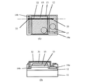
(参考例1)
図1は、本発明に密接に関連する参考例1のLED素子を示す図で、(A)は上面図、(B)は断面図である。図において、11はサファイア基板、12はn−GaN層、13はp−GaN層、14aおよび14bは負電極、15は正電極、16は配線層である。また、上面図(A)において、円形の記号17でボンディング領域の概略を示した。
【0028】
図示されるように、本素子では、正電極15の下に、pn界面が存在し、上面から見た場合に、正電極もしくはp−GaN層の部分が発光部に対応していることになる。負電極14aおよび14bは、概略四角形の発光部の対向する2辺に沿って、配置されており、互いに配線層16で電気的に接続されている。14aはボンディングに必要な大きさを確保する程度に太く形成されており、14bはその必要がなく、円形の記号17で概略そのサイズが示されているボンディング領域よりも、かなり細く形成されている。本参考例1においては、配線層16を、発光部横の両側に設け、また、負電極14a,14bおよび配線層16を一体として形成したので、発光部が、これらにより囲まれるような配置となっている。
【0029】
このような発光素子の製造方法を、以下に述べる。サファイア基板上11に、n−GaN層12(層厚4μm、Siドープ)、p−GaN層13(層厚0.5μm、Mgドープ)を順次積層する。その後、フォトリソグラフィー技術とドライエッチング技術を用い、ウェハー表面よりn−GaN層12の途中まで、素子の周辺部および、n電極を形成する部分を除去する。エッチングされなかったメサ状の部分にのみpn界面が残され、これが発光部に相当することとなる。本参考例1においては、発光部のサイズを200μm角とした。
【0030】
次いで、p−GaN層13上に、正電極15を形成する。電極材料として、例えば、Ni/AuあるいはPd/Au等を用いればよい。正電極は、光取り出しを側面もしくは基板側からのみ行う場合には、ボンディングが容易なように、例えば1μmと一括して厚く形成すればよく、逆に光取り出しを、正電極を通して表面側から行う場合には、光透過性とするために、ボンディング領域17を除いて、10nm程度の薄い膜厚で形成する必要がある。
【0031】
また、n−GaN層12上には、負電極14a,14bおよび配線層16を一体として形成する。材料として、例えば、AlあるいはTi/Au、またあるいはW/Au等を用いればよい。負電極の形状として、ボンディングを行う側の14aは、太くする必要がある。具体的には、ボンディングのためには、通常80μmφ以上のエリアが必要となるので、幅80μm以上とすればよい。逆に、14bは、細くして、素子サイズの増大を押さえることが望ましい。具体的には、電極幅として、2〜10μm程度が適当である。この程度の線幅でも、電極として、n型半導体層へ、電流を十分に供給でき、問題とはならない。また、配線層の幅に関しては、2μm程度で十分である。本参考例1においては、負電極と配線層を一括して設けたので、工程が簡略化されている。
【0032】
以上の工程は、ウェハー上でなされ、その後、四辺形状に、各素子が切り出されて、図1に示すLED素子が完成する。
【0033】
最終的には、光取り出しを表面もしくは側面から行う場合、基板を下にして、適切な台座の上に素子を固定した後、17で示される領域に、ワイヤボンディングがなされ、LED素子が完成する。
【0034】
あるいは、光取り出しを基板から行う場合には、17で示される領域を電気的な接続点とし、表面を下にした、いわゆるフリップチップボンディング法によって、適切な台座の上に素子が固定され、LED素子が完成する。
【0035】
以上のように、本参考例1の形態においては、正電極が、発光部ほぼ全面を覆い、負電極が、概略四角形の発光部の対向する2辺に沿って配置されるので、発光部に電流が均一に注入される。
【0036】
本参考例1の効果を確認するために、正電極を透明な薄膜電極とし、駆動電流5mAにおける発光強度分布を、正電極を通して観察した。この程度の駆動電流では、高電流密度効果による発光効率低下がほとんど無視できるので、発光強度分布は、注入電流分布にほぼ1対1に対応する。このような、観察により、n−GaN層の層厚が2μm以上で、ドーピング濃度が5×10¹⁷〜2×1019cm-3の範囲であれば、発光部サイズを300μm角以内とすることで、ほぼ均一な電流注入が可能であることが判明した。発光部サイズをこれより大きくすると、中央部の発光強度が負電極近傍から1割以上低下した。
【0037】
なお、本参考例1においては、配線層と負電極が一括して形成されており、配線層自体も、負電極としての機能を有していることになる。しかしながら、配線層下に絶縁物を設け、配線層がn−GaN層に接触しないようにしても、発光部における均一電流注入条件には、ほとんど影響しなかった。これにより、電流分布を抑制するためには、適正な大きさの発光部の両側に、対向して負電極を設けることが重要であることが示された。
【0038】
このように、本参考例1によれば、pn界面を流れる電流の分布が小さくなり、その結果、発光部全体から均一な発光を得ることができた。
【0039】
これにより、負電極を、発光部の片方にのみ配置した発光素子と比較して、輝度が大きく、発光効率が良く、さらには、駆動電流変化による放射光パターンシフトの無い素子を、得ることができた。
【0040】
また、本参考例1の発光素子においては、負電極を発光部の両側に対向させて配置する際に、その片側を、ボンディングに要する太さよりも極めて細く形成したので、これによる素子サイズの増大は、製造工程上のマスク合わせの余裕を考慮しても、10〜20μm幅であり、わずかであった。
【0041】
さらに、本参考例1の発光素子においては、発光部の両側に設けられた負電極を配線層で電気的に接続したので、負側のボンディングが1回で良く、製造工程が簡略である。また、本参考例1の発光素子においては、配線層の幅を2μmと、発光部のサイズと比較して、極めて小さく形成したので、これによる素子サイズの増大は、製造工程上のマスク合わせの余裕を考慮しても、各々10〜20μm幅であり、わずかであった。
【0042】
なお、本参考例1において、基板、各半導体層、電極材料を上述のものとしたが、これらは、公知のとおり、必要に応じて変更され得るものである。
【0043】
(参考例2)
図2は、本発明に密接に関連する参考例2のLED素子を示す図で、(A)は上面図(B)は断面図である。図において、参考例1と同様の部分は、同一の記号で表示した。
【0044】
図示されるように、本参考例2の発光素子は、参考例1の発光素子の変形であり、発光部(正電極)および負電極の形状が異なる。本素子では、負電極14aは、ボンディングに必要な領域部分のみが太く形成され、残りの部分が細くなっている。その分、発光部が横に張り出して、参考例1と比較して、面積が広がることにつながっている。したがって、参考例1と同じ素子サイズでも、発光面積を広くできる。また、本素子では、配線層は、発光部の片側にしか設けられておらず、その分、参考例1と比較して、素子サイズをさらに縮小できる。
【0045】
本参考例2によれば、負電極を発光部の両側に対向させて配置したので、pn界面を流れる電流の分布が小さくなり、その結果、発光部全体から均一な発光を得ることができた。
【0046】
これにより、負電極を、発光部の片方にのみ配置した発光素子と比較して、輝度が大きく、また、発光効率が良く、駆動電流変化による放射光パターンシフトの無い素子を、得ることができた。
【0047】
また、本参考例2の発光素子においては、負電極を発光部の両側に対向させて配置する際に、その片側を、ボンディングに要する太さよりも極めて細く形成したので、これによる素子サイズの増大は、製造工程上のマスク合わせの余裕を考慮しても、10〜20μm幅であり、わずかであった。
【0048】
さらに、本参考例2の発光素子においては、発光部の両側に設けられた負電極を配線層で電気的に接続したので、負側のボンディングが1回で良く、製造工程が簡略である。また、本参考例2の発光素子においても、配線層の幅を3μmと、発光部のサイズと比較して、極めて小さく形成したので、これによる素子サイズの増大は、製造工程上のマスク合わせの余裕を考慮しても、10〜20μm幅であり、わずかであった。
【0049】
(実施の形態1)
図3は、本発明の実施の形態1のLED素子を示す図で、(A)は上面図(B)は断面図である。図において、11はサファイア基板、12はn−GaN、13はp−GaN、14aおよび14bは負電極、15は正電極、31は絶縁膜、32は配線層である。上面図において、円形の記号17でボンディング領域の概略を示した。さらに、上面図では、分かりやすくするために絶縁膜31を省略しており、黒丸の記号33で、重なって描かれている金属層間の電気的な接続を表現している。
【0050】
図示されるように、本素子では、負電極が2つに分割されて、概略四角形の発光部の対向する2辺に沿って、配置されており、互いに、発光部の上方に設置された配線層で電気的に接続されている。負側のボンディングは14aのみでなされることになり、14aはボンディングに必要な大きさを確保するために、太く形成されており、14bはその必要がなく、細く形成されている。
【0051】
このような発光素子の製造方法を、以下に述べる。サファイア基板上11に、n−GaN層12(膜厚4μm、Siドーピング)、p−GaN層13(膜厚0.7μm、Mgドーピング)を順次積層する。その後、フォトリソグラフィー技術とドライエッチング技術を用い、ウェハー表面よりn−GaN層12の途中まで、素子の周辺部および、負電極を形成する部分を除去する。エッチングされなかったメサ状の部分にのみpn界面が残され、これが発光部に相当することとなる。本実施の形態においては、発光部のサイズを150μm角とした。
【0052】
次いで、p−GaN層13上に、正電極15を形成する。電極材料として、例えば、Ni/AuあるいはPd/Au等を用いればよい。正電極は、光取り出しを基板もしくは側面から行う場合には、ボンディングが容易なように、例えば1μmと一括して厚く形成すればよく、逆に光取り出しを表面側から行う場合には、光透過性とするために、ボンディング領域17を除いて、10nm程度に薄く形成する必要が有る。
【0053】
また、n−GaN層12上には、負電極14a,14bを形成する。電極材料として、例えば、Al、あるいはTi/Au、またあるいはW/Au等を用いれば、良好な電気的接触が得られる。負電極は、ボンディングが容易に行えるように、例えば1μm程度に厚く形成し、さらに、表面がAlもしくはAuからなることが望ましい。負電極形成の際、図1に示したような負電極および配線層形状の発光素子と異なり、本実施の形態の発光素子では、負電極14a、発光部、負電極15bが一列に並んで配置されているので、並んだ方向と垂直の方向に、負電極の配置が多少ずれても、負電極が発光部に重なってしまう不具合が生じない。これにより、製造工程上の余裕ができ、発光素子生産性の向上に貢献する。
【0054】
負電極の形状として、ボンディングを行う側の14aは、太くする必要がある。具体的には、ボンディングのためには、通常80μmφ以上のエリアが必要となるので、幅80μm以上とすればよい。逆に、14bは、製造工程上適当な程度まで細くし、素子サイズの増大を押さえることが望ましい。具体的には、電極幅として、2〜10μm程度が適当である。この程度の線幅でも、電極として、n型半導体層内部に、電流を十分に供給でき、問題とはならない。
【0055】
その後、ウェハー表面に絶縁膜31を形成し、フォトリソグラフィー技術とエッチング技術を用いて、分割されたそれぞれの負電極上の適切な位置に開口部を設け、開口部を通じてそれぞれの負電極が電気的に接続されるように、配線層32を形成する。各要素の材料としては、例えば、絶縁膜31に、SiO2あるいはSiNを用いれば良く、配線層32に、Alを用いれば良い。このような配線層32は通常の薄膜形成技術と選択エッチング技術により形成できる。
【0056】
その後、図3には示されないが、必要に応じて、配線層32を絶縁膜で覆ってもよい。以上の工程は、ウェハー上でなされ、その後、四辺形状に、各素子が切り出されて、図3に示すLED素子が完成する。
【0057】
最終的には、光取り出しを表面もしくは側面から行う場合、基板を下にして、適切な台座の上に素子を固定した後、17で示される領域に、ワイヤボンディングがなされ、LED素子が完成する。
【0058】
あるいは、光取り出しを基板側から行う場合には、17で示される領域を電気的な接続点とし、表面を下にした、いわゆるフリップチップボンディング法によって、適切な台座の上に素子が固定され、LED素子が完成する。
【0059】
本発明の効果を確認するために、正電極を透明な薄膜電極として、駆動電流5mAにおける発光強度分布を、正電極を通して観察した。この程度の駆動電流では、高電流密度効果による発光効率低下がほとんど無視できるので、発光強度分布は、注入電流分布にほぼ1対1に対応する。このような、観察により、n−GaN層の層厚が2μm以上で、ドーピング濃度が1×10¹⁸〜2×1019cm-3の範囲であれば、発光部サイズを300μm角以内とすることで、ほぼ均一な電流注入が可能であることが判明した。
【0060】
このように、本実施の形態によれば、正電極が発光部のほぼ全面を覆うように設けられ、また、負電極を発光部の両側に対向させて配置したので、pn界面を流れる電流の分布が小さくなり、その結果、発光部全体から均一な発光を得ることができた。また、負電極のサイズについては、14aはボンディングのために幅80μm以上必要であるが、その反対側14bについては、3〜10μmで十分である。そのため、pn界面に電流を均一に注入するために、電極を分割しても、素子サイズの増大はごくわずかで済む。
【0061】
これにより、負電極を、発光部の片方にのみ配置した発光素子と比較して、輝度が大きく、また、発光効率が良く、駆動電流変化による放射光パターンシフトの無い素子を、得ることができた。
【0062】
また、本実施の形態の発光素子においては、負電極を発光部の両側に対向させて配置する際に、その片側を、ボンディングに要する太さよりも極めて細く形成したので、これによる素子サイズの増大は、製造工程上のマスク合わせの余裕を考慮しても、10〜20μm幅であり、わずかであった。
【0063】
さらに、本実施の形態の発光素子においては、発光部の両側に設けられた負電極を配線層で電気的に接続したので、負側のボンディングが1回で良く、製造工程が簡略である。また、配線層は正電極の上方ならば、どこに配置しても良いので、これを配置するためのマスク合わせ工程にはさほど厳密性を要求されない。さらに、配線層を配置するための素子サイズの増大が全くないので、参考例1ないし2の発光素子と比較して、さらに効率的な構成となっている。
【0064】
配線層のサイズについては、分割された負電極間で顕著な電位差が生じないように考慮すれば良い。これは次のような考えに基づいて設計できる。例えば、発光部の大きさとして150μm角を仮定し、Al配線層が長さ200μmとなる場合を考えると、配線層断面が2μm角のとき、抵抗が約1.4Ωとなる。LEDの定格電流は、典型的には20mAであるから、そのうちの半分の電流が配線層を流れると考えて、両負電極間の電位差はわずか0.014Vであり、実質問題とならない程度に抑えられることが理解できる。
【0065】
このように、配線層のサイズは、発光部のサイズよりも十分に小さくできるので、正電極を透明電極として、ここから光を取り出すような構成にしても、透明電極の上に設けられた配線層が光取り出しに影響することをほとんど無くすることが可能である。この点が、分割された負電極同士をワイヤーで接続するような方法と異なる。
【0066】
本実施の形態における配線層の材料は、Alの他にも、Au、Cuなどの金属を用いても良く、また、ITOなどの、非金属製導電性材料を用いても良い。さらに、配線層は単層に限るものではなく、複数の材料の積層構造としても、本発明の趣旨を逸脱するものではない。積層構造にすることで、配線層の最下層に、絶縁体膜との密着性が良好な材料を選定し、配線層の上層には、抵抗率の低い材料を選定するといった改良を行うことが可能になる。
【0067】
なお、本実施の形態においては、配線層の数を1本としたが、これに平行して、複数本の構成としても良い。配線層の数を数本としても、配線層が十分に細いので、正電極からの光の取り出しには全く影響を与えない。配線層の数を増やすことで、たとえ、一部の配線層の形成や接続に不良が生じても、素子機能不良が生じなくなり、製造工程上のマージンが取れることになる。
【0068】
さらに、本実施の形態においては、配線層を正電極の上方に設けたが、これを、正電極とp−GaN層の間に設けるなどのバリエーションも可能である。この場合、配線層を正電極およびp−GaN層と絶縁する必要があり、製造工程が複雑化することになる。
【0069】
なお、本実施の形態においては、負電極を2分割した例を示したが、本発明によれば、分割数を3以上とするような変形も可能である。
【0070】
また、本実施の形態において、基板、各半導体層、絶縁膜材料、電極材料を上述のものとしたが、これらは、公知のとおり、必要に応じて変更され得るものである。
【0071】
(実施の形態2)
図4は、本発明の実施の形態2のLED素子を示す図で、(A)は上面図(B)は断面図である。図において、実施の形態1と同じ部分は、図3と同じ記号で示した。また、41はボンディングパッドである。なお、上面図では、分かりやすくするために絶縁膜31を省略し、黒丸の記号33で、重なり合って描かれている金属層間の電気的な接続を表した。
【0072】
図4に示されるように、本実施の形態は、実施の形態1の変形例であり、正電極15に接続されたボンディングパッド41が、負電極14aとは絶縁膜31により電気的に分離され、負電極14aの一部を覆う形で設けられた点が異なる。
【0073】
本実施の形態のLED素子の製造方法については、実施の形態1と同様の素子構造を作製した後に、絶縁膜31の一部に、開口部を設け、これを通じて、正電極15と直接接触するように、ボンディングパッド41を設ける工程が加わる他は、実施の形態1と同様であるので詳細を省略する。なお、ボンディングパッド41は、配線層32と同時に形成することが可能である。本実施の形態においては、発光部のサイズを100μm角とした。正電極を透明とし、表面から光を取り出すタイプのLEDの場合、実施の形態1の発光素子では、光取り出しがボンディング領域を除くL字型の部分からしか出来なかったのに対し、本実施の形態では、正側のボンディングが、正電極から横に引き出されたパッド上になされるので、ボンディング領域が光の取り出しを妨害することが無くなり、ほぼ正電極全面から光を取り出すことが出来る。これにより、実施の形態1と比較して、光取り出し効率を向上出来るほか、光取り出しパターンを正方形に近くでき、従って、素子からの光放射パターンを縦横で一致させることができる。さらに、ボンディングパッド41は負電極14aに重ねて形成されるので、このような効果を付加するに当たっては、素子サイズを大きくする必要がないのである。また、素子の両側にボンディングパッドが設けられた、図7に示す発光素子では、正電極を通した発光部からの光取り出しを妨害しないように、ボンディングワイヤーが発光部をまたがず接続するためには、正負それぞれのボンディングを素子の反対側から行う必要があったが、本実施の形態の素子では、ボンディングパッドが素子の片側に設けられているので、ボンディングを素子の片側からのみ行うことが可能である。これにより、ボンディング工程が簡略になる。
【0074】
また、本実施の形態においても、実施の形態1と同様の効果により、輝度が大きく、また、発光効率が良く、駆動電流変化による放射光パターンシフトの無い発光素子を、素子サイズを無用に増大する事なく、得ることができた。
【0075】
(実施の形態3)
図5は、本発明の実施の形態3のLED素子を示す図で、(A)は上面図、(B)は断面図である。図において、実施の形態1と同じ部分は、図3と同じ記号で示した。また、51aおよび51bは負電極であり、52は配線層を兼ねたボンディングパッドである。なお、上面図では、分かりやすくするために絶縁膜31を省略し、黒丸の記号33で、重なり合って描かれている金属層間の電気的な接続を表した。
【0076】
図5に示されるように、本実施の形態は、実施の形態1の変形例であり、本LED素子では、負電極51aおよび51bに電気的に接続された配線層兼ボンディングパッド52が正電極15の一部を覆う形で、正電極15とは絶縁膜31により電気的に分離されて設けられた点が異なる。本実施の形態においては、発光部のサイズを250μm角とした。本実施の形態のLED素子の製造方法については、実施の形態1と同様の製造工程にて、素子構造を作製した後に、絶縁膜31の一部に開口部を設け、これを通じて、負電極14a,14bと直接接触するように、配線層兼ボンディングパッド52を設ける工程が加わる他は、実施の形態1と同様であるので詳細を省略する。
【0077】
本実施の形態では、正電極上に、正負両方のボンディングパッドが設けられており、正電極を通じた光取り出しができないので、側面もしくは裏面から光を取り出すタイプのLEDに応用される。本実施の形態によれば、負電極51aおよび51bの幅は、いずれについてもボンディングに必要な領域を確保する必要がないので、従来の技術や、あるいは、実施の形態1に示したLED素子と比べて格段に小さくすることが可能になる。通常、図5において、各負電極の幅は、2〜10μmで十分であり、したがって、素子のサイズは、通常100μm角以上の大きさを有している発光部に若干の面積を付加した程度でよく、格段に素子サイズを小さくすることができるのである。
【0078】
また、製造工程上、エッチング面が時折平坦でなく、この場合、参考例1と2および実施の形態1と2では、エッチング面上に設けられた負電極表面が凹凸をもち、ボンディング不良が生じることがあったけれども、本実施の形態では、正負両側のボンディングが正電極上で行われるので、このような不具合が生じることが避けられる。
【0079】
また、本実施の形態においても、実施の形態1と同様の効果により、輝度が大きく、また、発光効率が良く、駆動電流変化による放射光パターンシフトの無い発光素子を、素子サイズを無用に増大する事なく、得ることができた。
【0080】
以上、本発明をGaN系LED素子に適用した実施の形態1ないし3では、各層を上記特定の材料に限定した例で記載したが、これは、本発明の本質にかかわるものではなく、公知の技術に基づいて、変更可能なものである。例えば、pn界面付近に、InGaN発光層を設けたり、GaN層に加えてAlGaN層を付加したりしても、本発明の効用がなんら変更され得るものではない。
【0081】
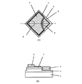
(実施の形態4)
本発明の実施の形態4は、実施の形態1と同様の電極配置を、半導体レーザ素子に応用した例である。図6は、実施の形態4の半導体レーザ素子を示す図で、(A)は上面図(B)は断面図である。図において、61はサファイア基板、62はn−AlGaN層クラッド層、63はInGaN層活性層、64はp−AlGaN層クラッド層、65aおよび65bは負電極、66は正電極、67は絶縁膜、68は配線層であり、円形の記号17でボンディング領域を概略示している。なお、上面図では、分かりやすくするために絶縁膜67を省略し、黒丸の記号33で、重なり合って描かれている金属層間の電気的な接続を表した。
【0082】
本実施の形態は、本発明を半導体レーザに応用した例であり、その、目的とするところは、発光部に均一に電流を注入することにあり、実施の形態1ないし3に準じる。図6に示されるように、本実施の形態では、発光部である活性層63がストライプ状に設けられており、その両側に、平行して、負電極を設け、それぞれを配線層68で電気的に接続した。配線層68を設けなければ、それぞれの負電極にボンディングを行う必要があったのに対して、本実施の形態によれば、ボンディングが65a側の一回で良く、製造工程が簡略化され、素子サイズが無用に大きくなることも避けられる。
【0083】
本実施の形態によれば、ボンディング工程を複雑化することなく、分割された負電極への電流供給が可能になり、活性層への電流の均一注入が実現できる。
【0084】
また、本実施の形態において、基板、各半導体層の材料を上述のものとしたが、これらは、公知の技術に基づき、必要に応じて変更され得るものである。
【0085】
以上、本発明に基づく実施の形態では、基板として、絶縁基板であるサファイアについて例示したが、本発明は、絶縁基板の場合に特定される訳ではなく、導電性基板を用いるときにも適用が可能である。これは、特に、基板に電極を取っても、半導体層と導電性基板との間に顕著な電圧降下が生じてしまう場合や、素子マウントの構成上、表面側から正負電極を取りたい場合などに有効である。前者の例としては、導電性SiC基板上に設けた、GaN層系発光素子が挙げられ、後者の例としては、フリップチップボンディングのようなLED素子の積載方法を採用する場合が挙げられる。
【0086】
また、本発明に基づく実施の形態の例を、主に、III族元素窒化物半導体発光素子の例で述べたが、本発明の適用範囲はこれに限られるものではなく、例えば、AlGaAs系半導体発光素子、AlGaInP系発光素子、GaAsP系発光素子などにも適用が可能であることは、容易に推察され得る。
【0087】
【発明の効果】
本発明によれば、上記構成によって、ボンディング工程を複雑化したり、素子サイズを無用に増大させることなく、第2電極下のpn界面に均一に電流を供給でき、これにより、上面より正負両電極を取るタイプの発光素子の輝度向上、発光効率向上などに貢献する。
【図面の簡単な説明】
【図1】 本発明に密接に関連する参考例1におけるLED素子を示す上面および断面図である。
【図2】 本発明に密接に関連する参考例2におけるLED素子を示す上面および断面図である。
【図3】 本発明の実施の形態1におけるLED素子を示す上面および断面図である。
【図4】 本発明の実施の形態2におけるLED素子を示す上面および断面図である。
【図5】 本発明の実施の形態3におけるLED素子を示す上面および断面図である。
【図6】本発明の実施の形態4における半導体レーザ素子を示す上面および断面図である。
【図7】 従来の技術に基づく発光素子を示す上面および断面図である。
【符号の説明】
11 サファイア基板
12 n−GaN層
13 p−GaN層
14a、14b 負電極
15 正電極
16 配線層
17 ボンディングの概略位置
31 絶縁膜
32 配線層
33 上面図において重なり合う金属層間の電気的接続を示す記号
41 正電極に接合するボンディングパッド
51a、51b 負電極
52 配線層兼ボンディングパッド
61 サファイア基板
62 p−AlGaN層クラッド層
63 InGaN層活性層
64 n−AlGaN層クラッド層
65a、65b 負電極
66 正電極
67 絶縁膜
68 配線層[0001]
BACKGROUND OF THE INVENTION
The present invention relates to a form of an electrode of a light emitting element having a structure in which positive and negative electrodes are arranged on the surface.
[0002]
[Prior art]
In recent years, semiconductor light emitting devices such as LEDs that emit light in the ultraviolet to visible region have been realized with nitride semiconductor materials typified by GaN, AlN, InN, or mixed crystals thereof. Since sapphire which is an insulator is used as a substrate, an element shape different from a normal light emitting element using a conductive substrate is employed.
[0003]
FIG. 7 is a schematic view showing an LED element using a nitride semiconductor material according to such a technique.
[0004]
In FIG. 7, 1 is a sapphire substrate, 2 is an n-GaN layer, 3 is a p-GaN layer, 4 is a negative electrode, and 5 is a positive electrode. In order to feed power to the element from the outside, wire bonding or the like is performed on each electrode and used. Such a bonding region is schematically indicated by a circular symbol 6. In the present element, the pn interface immediately below the positive electrode is the light emitting portion, and the portion other than the bonding region of the positive electrode is formed of a very thin metal film, so that the emitted light can be extracted from here.
[0005]
As described above, since the insulating substrate is used, the point that the positive and negative electrodes are arranged on the surface of the wafer is different from a normal LED element.
[0006]
[Problems to be solved by the invention]
However, the above conventional techniques have the following problems.
[0007]
In a light emitting device of a type in which positive and negative electrodes are arranged on the wafer surface, current flows basically in a direction parallel to the surface. Therefore, it is difficult to uniformly inject current into the pn interface formed in parallel to the device surface, and uneven light emission. It is easy to produce.
[0008]
As a phenomenon peculiar to nitride semiconductor light-emitting devices using GaN or InGaN as the light-emitting layer, the light emission efficiency may decrease when the current density increases. The luminous efficiency of the device as a whole is poor, and the luminous efficiency of the entire device is worse than that in which uniform current is injected into the pn interface. Therefore, in order to obtain a required luminance at a predetermined element driving current, an element that generates unevenness in light emission needs to have a larger light emitting portion than that in the case of uniform light emission, that is, the element size is increased. There is a problem in that the manufacturing cost increases.
[0009]
Further, even in an element that exhibits non-uniform light emission when the element drive current is small, the light emission distribution itself is reduced because the light emission efficiency decreases from the high current density region as the drive current is increased. This means that the light emission position changes depending on the drive current. In particular, in an application in which the drive current is changed for the purpose of gradation display or the like, there is a disadvantage that the emitted light pattern is shifted.
[0010]
In order to solve the above-mentioned problems, it is important to devise a method for allowing a current to flow uniformly in the light emitting portion. In the element shown in FIG. 7, a positive electrode is formed so as to cover almost the entire surface of the p-GaN layer. Attempts have been made to improve this point. However, since the negative electrode is provided only on one side of the light emitting part, it is not always possible to avoid uneven light emission due to insufficient current spreading in the n-GaN layer under the light emitting part.
[0011]
The present invention has been made in view of the above points, and the current distribution is improved without increasing the size unnecessarily and without increasing the bonding locations more than necessary.RuThus, a semiconductor light emitting device structure that solves the above problems is realized.
[0012]
[Means for Solving the Problems]
The light emitting device of the present invention includes a first conductive type semiconductor layer provided directly or indirectly on a substrate, and an integrated second conductive type semiconductor layer provided on a part of the first conductive type semiconductor layer. A second electrode provided on the first conductive type semiconductor layer on the first conductive type semiconductor layer without the second conductive type semiconductor layer; and a second electrode provided on the second conductive type semiconductor layer so as to cover the entire surface. By having the electrode, in the top view, the portion of the second conductivity type semiconductor layer is a semiconductor light emitting element constituting the light emitting portion, and the first electrode includes at least one side of the light emitting portion, Provided on opposite sides, and at least one of them is formed narrower than the width of the region required for bonding, andAbove the second conductivity type semiconductor layerIt is electrically connected by a wiring layer provided inThe
[0013]
TheFurthermore, in a light emitting device according to another aspect of the present invention, a first conductivity type semiconductor layer and a second conductivity type semiconductor layer are sequentially provided on a substrate, and the second conductivity type semiconductor layer is provided on the first conductivity type semiconductor layer. A first electrode provided on a portion without the conductive type semiconductor layer; and a second electrode provided on the second conductive type semiconductor layer, wherein the first electrode is the second conductive type layer in a top view. The first electrodes arranged on both sides of the portion provided with the electrode are electrically connected to each other by a wiring layer provided on the second electrode via an insulating layer. It is characterized by.
[0014]
Preferably, the light emitting device of the present invention is provided with a bonding pad that covers the part of the first electrode and is bonded to the second electrode.
[0015]
Preferably, the light emitting device of the present invention is provided with a bonding pad that covers a part of the second electrode and is bonded to the wiring layer.ThisThe
[0016]
In the case where the first electrode is disposed on both sides of the portion where the second conductivity type layer is provided, a bonding pad portion may be provided on one of the first electrodes disposed on both sides.
[0017]
In the light emitting device of the present invention, the first conductive semiconductor layer is composed of one or more group III element nitride semiconductors, and the second conductive semiconductor layer is composed of one or more group III element nitrides. Consists of physical semiconductors
[0018]
In this specification, each conductivity type is selected from p-type, n-type and i-type.
[0019]
Based on the above-described configuration, the operation will be described next.
In the present invention, at least one side of the light emitting part, the first electrode provided on the opposite side, and the second electrode provided on the second conductive semiconductor layer so as to cover the entire surface are mutually It has the effect of supplying current uniformly to semiconductor interfaces of different conductivity types.
[0020]
Further, by forming at least one of the first electrodes narrower than the width of the region required for bonding, it is possible to secure a bonding region necessary for electrically connecting the first electrode to the outside. The first electrode can be efficiently disposed on the element.
[0021]
In the present invention, the wiring layer provided on the surface of the light emitting element can supply current to the respective portions of the first electrode provided on both sides of the light emitting portion by one bonding to the first electrode. To.
[0022]
In particular, by providing the wiring layer above the second conductivity type semiconductor layer, there is no need for a new region for providing the wiring layer on the element, and mask alignment in the manufacturing process is eliminated. Tolerance is expanded.
[0023]
Furthermore, by providing a bonding pad to be bonded to the second electrode so as to cover a part of the first electrode, it is possible to supply current to the second electrode without substantially obstructing light extraction from the second electrode. In addition, a region for providing such a bonding pad is not required on the element.
[0024]
Furthermore, by providing a bonding pad that is bonded to the wiring layer and covers a part of the second electrode, the area of the first electrode is secured while securing a bonding place for supplying current to the first electrode. Can be minimized, and the element size can be reduced to approximately the size of the light emitting portion.
[0025]
The first conductive semiconductor layer is composed of one or more Group III element nitride semiconductors, and the second conductive semiconductor layer is composed of one or more Group III element nitride semiconductors. Thus, there is no current distribution in the light emitting portion, and as a result, a light emitting element that emits light in the ultraviolet to visible region with high efficiency, no shift of the emitted light pattern due to the drive current, and reduced element size can be realized.
[0026]
DETAILED DESCRIPTION OF THE INVENTION
In the following, various embodiments according to the present invention will be described, together with some reference examples closely related to the present invention.
[0027]
(Reference example1)
FIG. 1 shows the present invention.Reference examples closely related toIt is a figure which shows 1 LED element, (A) is a top view, (B) is sectional drawing. In the figure, 11 is a sapphire substrate, 12 is an n-GaN layer, 13 is a p-GaN layer, 14a and 14b are negative electrodes, 15 is a positive electrode, and 16 is a wiring layer. Further, in the top view (A), the outline of the bonding region is indicated by a
[0028]
As shown in the figure, in this element, a pn interface exists under the
[0029]
A method for manufacturing such a light emitting element will be described below. On the
[0030]
Next, the
[0031]
On the n-
[0032]
The above steps are performed on the wafer, and thereafter, each element is cut out in a quadrilateral shape to complete the LED element shown in FIG.
[0033]
Ultimately, when light extraction is performed from the front or side, after fixing the element on an appropriate pedestal with the substrate facing down, wire bonding is performed in a region indicated by 17 to complete the LED element. .
[0034]
Alternatively, when light extraction is performed from the substrate, the element is fixed on an appropriate pedestal by a so-called flip chip bonding method in which the region indicated by 17 is an electrical connection point and the surface is down, The element is completed.
[0035]
As above, the bookReference example 1In this embodiment, since the positive electrode covers almost the entire surface of the light emitting portion and the negative electrode is disposed along two opposing sides of the substantially square light emitting portion, current is uniformly injected into the light emitting portion.
[0036]
BookReference example 1In order to confirm this effect, the positive electrode was a transparent thin film electrode, and the emission intensity distribution at a driving current of 5 mA was observed through the positive electrode. With such a driving current, the decrease in light emission efficiency due to the high current density effect is almost negligible, so the light emission intensity distribution substantially corresponds to the injected current distribution on a one-to-one basis. According to such observation, the n-GaN layer has a thickness of 2 μm or more and a doping concentration of 5 × 10 5.17~ 2x1019cm-3In this range, it has been found that substantially uniform current injection is possible by setting the light emitting portion size within 300 μm square. When the light emitting portion size was made larger than this, the light emission intensity at the central portion was reduced by 10% or more from the vicinity of the negative electrode.
[0037]
BookReference example 1In FIG. 2, the wiring layer and the negative electrode are collectively formed, and the wiring layer itself also has a function as a negative electrode. However, even if an insulator is provided under the wiring layer so that the wiring layer does not come into contact with the n-GaN layer, the uniform current injection condition in the light emitting portion is hardly affected. Thereby, in order to suppress current distribution, it was shown that it is important to provide a negative electrode oppositely on both sides of a light emitting part of an appropriate size.
[0038]
Like thisReference example 1According to the above, the distribution of current flowing through the pn interface is reduced, and as a result, uniform light emission can be obtained from the entire light emitting portion.
[0039]
As a result, it is possible to obtain an element having a large luminance, good luminous efficiency, and no radiation pattern shift due to a change in driving current, as compared with a light emitting element in which the negative electrode is disposed only on one side of the light emitting unit. did it.
[0040]
Also bookReference example 1In this light emitting device, when the negative electrode is disposed to face both sides of the light emitting portion, one side thereof is formed to be extremely narrower than the thickness required for bonding, and this increases the device size in the manufacturing process. Even considering the margin for mask alignment, the width was 10 to 20 μm, which was slight.
[0041]
In addition, bookReference example 1In the light-emitting element, since the negative electrodes provided on both sides of the light-emitting portion are electrically connected by the wiring layer, the negative-side bonding may be performed once and the manufacturing process is simplified. Also bookReference example 1In this light emitting device, the width of the wiring layer is 2 μm, which is extremely small compared to the size of the light emitting portion. , Each having a width of 10 to 20 μm, and slight.
[0042]
BookReference example 1In the above, the substrate, each semiconductor layer, and the electrode material are as described above, but these can be changed as necessary as known.
[0043]
(Reference example2)
FIG. 2 illustrates the present invention.Reference examples closely related to2A and 2B are diagrams showing an
[0044]
As illustrated, the bookReference example 2The light emitting element ofReference example1 is a modification of the light emitting element 1, and the shapes of the light emitting part (positive electrode) and the negative electrode are different. In the present element, the
[0045]
BookReference example 2According to the above, since the negative electrode is arranged to face both sides of the light emitting portion, the distribution of current flowing through the pn interface is reduced, and as a result, uniform light emission can be obtained from the entire light emitting portion.
[0046]
As a result, it is possible to obtain an element that has a higher luminance, better luminous efficiency, and no radiated light pattern shift due to a change in driving current, compared to a light emitting element in which the negative electrode is disposed only on one side of the light emitting section. It was.
[0047]
Also bookReference example 2In this light emitting device, when the negative electrode is disposed to face both sides of the light emitting portion, one side thereof is formed to be extremely narrower than the thickness required for bonding, and this increases the device size in the manufacturing process. Even considering the margin for mask alignment, the width was 10 to 20 μm, which was slight.
[0048]
In addition, bookReference example 2In the light-emitting element, since the negative electrodes provided on both sides of the light-emitting portion are electrically connected by the wiring layer, the negative-side bonding may be performed once and the manufacturing process is simplified. Also bookReference example 2In the light emitting device, the width of the wiring layer is 3 μm, which is extremely small compared to the size of the light emitting portion. , 10-20 μm wide and slight.
[0049]
(Embodiment1)
FIG. 3 is a diagram showing the LED element of Embodiment 1 of the present invention, in which (A) is a top view (B) is a cross-sectional view. In the figure, 11 is a sapphire substrate, 12 is n-GaN, 13 is p-GaN, 14a and 14b are negative electrodes, 15 is a positive electrode, 31 is an insulating film, and 32 is a wiring layer. In the top view, the outline of the bonding region is indicated by a
[0050]
As shown in the figure, in the present element, the negative electrode is divided into two parts, arranged along two opposing sides of the substantially square light emitting part, and the wirings installed above the light emitting part. Electrically connected in layersTheYes. The negative side bonding is performed only by 14a, and 14a is formed thick in order to secure the size necessary for bonding, and 14b is formed thin without the necessity.
[0051]
A method for manufacturing such a light emitting element will be described below. On the
[0052]
Next, the
[0053]
Further,
[0054]
As the shape of the negative electrode, the
[0055]
Thereafter, an insulating
[0056]
Thereafter, although not shown in FIG. 3, the
[0057]
Ultimately, when light extraction is performed from the front or side, after fixing the element on an appropriate pedestal with the substrate facing down, wire bonding is performed in a region indicated by 17 to complete the LED element. .
[0058]
Alternatively, when light extraction is performed from the substrate side, the element is fixed on an appropriate pedestal by a so-called flip chip bonding method in which the region indicated by 17 is an electrical connection point and the surface is down, The LED element is completed.
[0059]
In order to confirm the effect of the present invention, the positive electrode was used as a transparent thin film electrode, and the emission intensity distribution at a driving current of 5 mA was observed through the positive electrode. With such a driving current, the decrease in light emission efficiency due to the high current density effect is almost negligible, so the light emission intensity distribution substantially corresponds to the injected current distribution on a one-to-one basis. According to such observation, the n-GaN layer has a thickness of 2 μm or more and a doping concentration of 1 × 10 5.18~ 2x1019cm-3In this range, it has been found that substantially uniform current injection is possible by setting the light emitting portion size within 300 μm square.
[0060]
Thus, according to the present embodiment, the positive electrode is provided so as to cover almost the entire surface of the light emitting portion, and the negative electrode is disposed so as to face both sides of the light emitting portion, so that the current flowing through the pn interface The distribution became smaller, and as a result, uniform light emission could be obtained from the entire light emitting part. As for the size of the negative electrode, 14a needs to be 80 μm or more in width for bonding, but 3 to 10 μm is sufficient for the
[0061]
As a result, it is possible to obtain an element that has a higher luminance, better luminous efficiency, and no radiated light pattern shift due to a change in driving current, compared to a light emitting element in which the negative electrode is disposed only on one side of the light emitting section. It was.
[0062]
Further, in the light emitting element of the present embodiment, when the negative electrode is disposed opposite to both sides of the light emitting part, one side thereof is formed to be extremely narrower than the thickness required for bonding, and this increases the element size. In consideration of the margin for mask alignment in the manufacturing process, the width was 10 to 20 μm, which was slight.
[0063]
Furthermore, in the light emitting element of this embodiment, since the negative electrodes provided on both sides of the light emitting portion are electrically connected by the wiring layer, the bonding on the negative side may be performed once, and the manufacturing process is simplified. Further, since the wiring layer may be disposed anywhere as long as it is above the positive electrode, the strictness is not required for the mask alignment process for disposing the wiring layer. Furthermore, since there is no increase in the element size for arranging the wiring layer,Reference exampleCompared with the one or two light emitting elements, the structure is more efficient.
[0064]
The size of the wiring layer may be considered so that no significant potential difference occurs between the divided negative electrodes. This can be designed based on the following idea. For example, assuming that the size of the light emitting portion is 150 μm square and the Al wiring layer has a length of 200 μm, when the wiring layer cross section is 2 μm square, the resistance is about 1.4Ω. Since the rated current of the LED is typically 20 mA, assuming that half of the current flows through the wiring layer, the potential difference between the two negative electrodes is only 0.014 V, so that it does not cause a substantial problem. I can understand.
[0065]
Thus, since the size of the wiring layer can be made sufficiently smaller than the size of the light emitting portion, the wiring provided on the transparent electrode can be configured even if the positive electrode is used as a transparent electrode and light is extracted from here. It is possible to almost eliminate the influence of the layer on the light extraction. This is different from a method in which the divided negative electrodes are connected by a wire.
[0066]
In addition to Al, the wiring layer material in the present embodiment may use a metal such as Au or Cu, or may use a non-metallic conductive material such as ITO. Furthermore, the wiring layer is not limited to a single layer, and a laminated structure of a plurality of materials does not depart from the spirit of the present invention. By adopting a laminated structure, it is possible to make improvements such as selecting a material with good adhesion to the insulator film as the lowermost layer of the wiring layer and selecting a material with low resistivity as the upper layer of the wiring layer. It becomes possible.
[0067]
In the present embodiment, the number of wiring layers is one, but a plurality of wiring layers may be provided in parallel therewith. Even if the number of wiring layers is several, the wiring layers are sufficiently thin and do not affect the extraction of light from the positive electrode. By increasing the number of wiring layers, even if a defect occurs in the formation or connection of a part of the wiring layers, the device function failure does not occur and a margin in the manufacturing process can be obtained.
[0068]
Furthermore, in the present embodiment, the wiring layer is provided above the positive electrode, but variations such as providing the wiring layer between the positive electrode and the p-GaN layer are also possible. In this case, it is necessary to insulate the wiring layer from the positive electrode and the p-GaN layer, which complicates the manufacturing process.
[0069]
In the present embodiment, an example in which the negative electrode is divided into two parts has been shown. However, according to the present invention, the number of divisions can be changed to three or more.
[0070]
In the present embodiment, the substrate, each semiconductor layer, the insulating film material, and the electrode material are described above. However, as is well known, these can be changed as necessary.
[0071]
(Embodiment2)
FIG. 4 shows an embodiment of the present invention.2It is a figure which shows this LED element, (A) is a top view (B) is sectional drawing. In the figure, the embodiment1The same parts as those shown in FIG.
[0072]
As shown in FIG. 4, the present embodiment is the same as the embodiment.
[0073]
About the manufacturing method of the LED element of this Embodiment, Embodiment1Embodiments other than the step of providing an opening in a part of the insulating
[0074]
Also in this embodiment, the embodiment1As a result, it was possible to obtain a light-emitting element having high luminance, good light emission efficiency, and no radiation pattern shift due to a change in driving current without unnecessarily increasing the element size.
[0075]
(Embodiment3)
FIG. 5 shows an embodiment of the present invention.3It is a figure which shows this LED element, (A) is a top view, (B) is sectional drawing. In the figure, the embodiment1The same parts as those shown in FIG. Further, 51a and 51b are negative electrodes, and 52 is a bonding pad that also serves as a wiring layer. In the top view, for the sake of clarity, the insulating
[0076]
As shown in FIG. 5, the present embodiment is the same as the embodiment.1In this LED element, the wiring layer /
[0077]
This embodimentsoSince both positive and negative bonding pads are provided on the positive electrode and light cannot be extracted through the positive electrode, it is applied to a type of LED that extracts light from the side surface or the back surface. According to the present embodiment, the widths of the
[0078]
Also, on the manufacturing process, the etched surface is sometimes not flat, in this case,Reference Examples 1 and 2 andEmbodiment 1And 2In this embodiment, the negative electrode surface provided on the etched surface has irregularities and bonding failure may occur. However, in this embodiment, bonding on both the positive and negative sides is performed on the positive electrode. Can be avoided.
[0079]
Also in this embodiment, the embodiment1As a result, it was possible to obtain a light-emitting element having high luminance, good light emission efficiency, and no radiation pattern shift due to a change in driving current without unnecessarily increasing the element size.
[0080]
As mentioned above, Embodiment 1 thru | or which applied this invention to the GaN-type LED element thru | or3In the above description, each layer is described as being limited to the specific material described above. However, this is not related to the essence of the present invention and can be changed based on a known technique. For example, even if an InGaN light emitting layer is provided in the vicinity of the pn interface or an AlGaN layer is added in addition to the GaN layer, the utility of the present invention cannot be changed at all.
[0081]
(Embodiment4)
Embodiment of the present invention4The embodiment1This is an example in which the same electrode arrangement is applied to a semiconductor laser device. FIG. 6 shows an embodiment.4FIG. 2A is a top view and FIG. 2B is a cross-sectional view. In the figure, 61 is a sapphire substrate, 62 is an n-AlGaN layer cladding layer, 63 is an InGaN layer active layer, 64 is a p-AlGaN layer cladding layer, 65a and 65b are negative electrodes, 66 is a positive electrode, 67 is an insulating film,
[0082]
The present embodiment is an example in which the present invention is applied to a semiconductor laser, and the object is to inject current uniformly into the light emitting portion.3According to As shown in FIG. 6, in the present embodiment, the
[0083]
According to this embodiment, current can be supplied to the divided negative electrode without complicating the bonding process, and uniform injection of current into the active layer can be realized.
[0084]
In the present embodiment, the materials of the substrate and each semiconductor layer are described above. However, these can be changed as necessary based on a known technique.
[0085]
As described above, in the embodiment based on the present invention, the sapphire that is an insulating substrate is exemplified as the substrate. However, the present invention is not specified in the case of the insulating substrate, and can be applied when a conductive substrate is used. Is possible. This is especially the case when a significant voltage drop occurs between the semiconductor layer and the conductive substrate even if the electrode is placed on the substrate, or when it is desired to remove the positive and negative electrodes from the surface side due to the structure of the element mount. It is effective for. An example of the former is a GaN layer-based light emitting element provided on a conductive SiC substrate, and an example of the latter is a case of adopting a LED element stacking method such as flip chip bonding.
[0086]
Moreover, although the example of embodiment based on this invention was described mainly in the example of the group III element nitride semiconductor light-emitting device, the application range of this invention is not restricted to this, For example, an AlGaAs type semiconductor It can be easily guessed that the present invention can be applied to a light emitting element, an AlGaInP light emitting element, a GaAsP light emitting element, and the like.
[0087]
【The invention's effect】
According to the present invention, with the above configuration, a current can be supplied uniformly to the pn interface below the second electrode without complicating the bonding process and unnecessarily increasing the element size. This contributes to improving the brightness and light emission efficiency of the light-emitting elements that take the light.
[Brief description of the drawings]
FIG. 1 shows the present invention.Reference examples closely related to2 is a top view and a cross-sectional view showing an LED element in FIG.
FIG. 2Reference examples closely related toFIG. 2 is a top view and a cross-sectional view showing an LED element in FIG.
FIG. 3 shows an embodiment of the present invention.1It is the upper surface and sectional drawing which show the LED element in.
FIG. 4 is an embodiment of the present invention.2It is the upper surface and sectional drawing which show the LED element in.
FIG. 5 shows an embodiment of the present invention.3It is the upper surface and sectional drawing which show the LED element in.
FIG. 6 shows an embodiment of the present invention.4It is the upper surface and sectional drawing which show the semiconductor laser element in.
FIGS. 7A and 7B are a top view and a cross-sectional view showing a light emitting device based on a conventional technique.
[Explanation of symbols]
11 Sapphire substrate
12 n-GaN layer
13 p-GaN layer
14a, 14b Negative electrode
15 Positive electrode
16 Wiring layer
17 Approximate position of bonding
31 Insulating film
32 Wiring layer
33 Symbol showing electrical connection between overlapping metal layers in top view
41 Bonding pad bonded to positive electrode
51a, 51b Negative electrode
52 Wiring layer and bonding pad
61 Sapphire substrate
62 p-AlGaN layer clad layer
63 InGaN active layer
64 n-AlGaN layer clad layer
65a, 65b Negative electrode
66 Positive electrode
67 Insulating film
68 Wiring layer
Claims (6)
該第1電極は、少なくとも、該発光部の片側と、その対向する側に設けられており、かつ、少なくとも、それらのうちのひとつは、ボンディングに要する領域の幅よりも狭く形成されており、かつ、それぞれが、前記第2導電型半導体層の上方に設けられた配線層により、電気的に接続されていることを特徴とする発光素子。A first conductive type semiconductor layer provided directly or indirectly on a substrate, an integrated second conductive type semiconductor layer provided on a part of the first conductive type semiconductor layer, and the first conductive type semiconductor By having a first electrode provided on the layer without the second conductive type semiconductor layer and a second electrode provided on the second conductive type semiconductor layer so as to cover the entire surface, an upper surface is provided. In view, in the semiconductor light emitting device in which the portion of the second conductivity type semiconductor layer constitutes the light emitting portion,
The first electrode is provided on at least one side of the light emitting portion and the opposite side thereof, and at least one of them is formed narrower than the width of the region required for bonding, And each is electrically connected by the wiring layer provided above the said 2nd conductivity type semiconductor layer, The light emitting element characterized by the above-mentioned.
Priority Applications (1)
| Application Number | Priority Date | Filing Date | Title |
|---|---|---|---|
| JP12845197A JP3878715B2 (en) | 1997-05-19 | 1997-05-19 | Light emitting element |
Applications Claiming Priority (1)
| Application Number | Priority Date | Filing Date | Title |
|---|---|---|---|
| JP12845197A JP3878715B2 (en) | 1997-05-19 | 1997-05-19 | Light emitting element |
Publications (2)
| Publication Number | Publication Date |
|---|---|
| JPH10321912A JPH10321912A (en) | 1998-12-04 |
| JP3878715B2 true JP3878715B2 (en) | 2007-02-07 |
Family
ID=14985045
Family Applications (1)
| Application Number | Title | Priority Date | Filing Date |
|---|---|---|---|
| JP12845197A Expired - Fee Related JP3878715B2 (en) | 1997-05-19 | 1997-05-19 | Light emitting element |
Country Status (1)
| Country | Link |
|---|---|
| JP (1) | JP3878715B2 (en) |
Cited By (1)
| Publication number | Priority date | Publication date | Assignee | Title |
|---|---|---|---|---|
| US9614126B2 (en) | 2015-04-27 | 2017-04-04 | Nichia Corporation | Light emitting device |
Families Citing this family (8)
| Publication number | Priority date | Publication date | Assignee | Title |
|---|---|---|---|---|
| US6696223B2 (en) | 1999-02-19 | 2004-02-24 | Agilent Technologies, Inc. | Method for performing photolithography |
| JP4267122B2 (en) * | 1999-02-19 | 2009-05-27 | アバゴ・テクノロジーズ・イーシービーユー・アイピー(シンガポール)プライベート・リミテッド | Photolithographic method and apparatus configuration for performing photolithography |
| US6614056B1 (en) | 1999-12-01 | 2003-09-02 | Cree Lighting Company | Scalable led with improved current spreading structures |
| JP2003110139A (en) * | 2001-09-28 | 2003-04-11 | Sanyo Electric Co Ltd | Nitride semiconductor light emitting element |
| JP3906736B2 (en) * | 2002-04-22 | 2007-04-18 | 日亜化学工業株式会社 | Nitride semiconductor device |
| KR100616693B1 (en) | 2005-08-09 | 2006-08-28 | 삼성전기주식회사 | Semiconductor light emitting device |
| US7998761B2 (en) * | 2006-01-09 | 2011-08-16 | Seoul Opto Device Co., Ltd. | Light emitting diode with ITO layer and method for fabricating the same |
| JP2007287757A (en) | 2006-04-12 | 2007-11-01 | Rohm Co Ltd | Nitride semiconductor light-emitting element and its manufacturing method |
-
1997
- 1997-05-19 JP JP12845197A patent/JP3878715B2/en not_active Expired - Fee Related
Cited By (1)
| Publication number | Priority date | Publication date | Assignee | Title |
|---|---|---|---|---|
| US9614126B2 (en) | 2015-04-27 | 2017-04-04 | Nichia Corporation | Light emitting device |
Also Published As
| Publication number | Publication date |
|---|---|
| JPH10321912A (en) | 1998-12-04 |
Similar Documents
| Publication | Publication Date | Title |
|---|---|---|
| JP3956918B2 (en) | Light emitting diode | |
| KR100838197B1 (en) | Light emitting diode with improved current spreading performance | |
| US7285801B2 (en) | LED with series-connected monolithically integrated mesas | |
| CN109638032B (en) | light emitting diode array | |
| JP5992662B2 (en) | Monolithic optoelectronic semiconductor body and manufacturing method thereof | |
| US7994523B2 (en) | AC light emitting diode having improved transparent electrode structure | |
| US6969873B2 (en) | Nitride gallium compound semiconductor light emission device | |
| US11587972B2 (en) | Wafer level light-emitting diode array | |
| US20150255504A1 (en) | Wafer level light-emitting diode array | |
| US11139338B2 (en) | Wafer level light-emitting diode array | |
| KR20090043058A (en) | Light emitting diode package | |
| JP2011199221A (en) | Light emitting diode | |
| JP5125433B2 (en) | Semiconductor light emitting device and manufacturing method thereof | |
| TW201547058A (en) | Light emitting diode and method of fabricating the same | |
| JP5628064B2 (en) | Optical semiconductor device | |
| JP5713650B2 (en) | LIGHT EMITTING ELEMENT AND MANUFACTURING METHOD THEREOF | |
| US20110079798A1 (en) | Light emitting apparatus | |
| JP2011146750A (en) | Light emitting diode chip | |
| JP3878715B2 (en) | Light emitting element | |
| JP4635985B2 (en) | Light emitting diode | |
| US20210351332A1 (en) | Optoelectronic semiconductor component | |
| JP4120493B2 (en) | Light emitting diode and light emitting device | |
| US9559270B2 (en) | Light-emitting device and method of producing the same | |
| JPH10209494A (en) | Semiconductor light emitting device | |
| JP5772213B2 (en) | Light emitting element |
Legal Events
| Date | Code | Title | Description |
|---|---|---|---|
| A521 | Written amendment |
Free format text: JAPANESE INTERMEDIATE CODE: A523 Effective date: 20040422 |
|
| A621 | Written request for application examination |
Free format text: JAPANESE INTERMEDIATE CODE: A621 Effective date: 20040422 |
|
| RD03 | Notification of appointment of power of attorney |
Free format text: JAPANESE INTERMEDIATE CODE: A7423 Effective date: 20040422 |
|
| A977 | Report on retrieval |
Free format text: JAPANESE INTERMEDIATE CODE: A971007 Effective date: 20060811 |
|
| A131 | Notification of reasons for refusal |
Free format text: JAPANESE INTERMEDIATE CODE: A131 Effective date: 20060822 |
|
| A521 | Written amendment |
Free format text: JAPANESE INTERMEDIATE CODE: A523 Effective date: 20061010 |
|
| TRDD | Decision of grant or rejection written | ||
| A01 | Written decision to grant a patent or to grant a registration (utility model) |
Free format text: JAPANESE INTERMEDIATE CODE: A01 Effective date: 20061031 |
|
| A61 | First payment of annual fees (during grant procedure) |
Free format text: JAPANESE INTERMEDIATE CODE: A61 Effective date: 20061106 |
|
| R150 | Certificate of patent (=grant) or registration of utility model |
Free format text: JAPANESE INTERMEDIATE CODE: R150 |
|
| FPAY | Renewal fee payment (prs date is renewal date of database) |
Free format text: PAYMENT UNTIL: 20091110 Year of fee payment: 3 |
|
| FPAY | Renewal fee payment (prs date is renewal date of database) |
Free format text: PAYMENT UNTIL: 20101110 Year of fee payment: 4 |
|
| FPAY | Renewal fee payment (prs date is renewal date of database) |
Free format text: PAYMENT UNTIL: 20111110 Year of fee payment: 5 |
|
| FPAY | Renewal fee payment (prs date is renewal date of database) |
Free format text: PAYMENT UNTIL: 20111110 Year of fee payment: 5 |
|
| FPAY | Renewal fee payment (prs date is renewal date of database) |
Free format text: PAYMENT UNTIL: 20121110 Year of fee payment: 6 |
|
| FPAY | Renewal fee payment (prs date is renewal date of database) |
Free format text: PAYMENT UNTIL: 20121110 Year of fee payment: 6 |
|
| FPAY | Renewal fee payment (prs date is renewal date of database) |
Free format text: PAYMENT UNTIL: 20131110 Year of fee payment: 7 |
|
| LAPS | Cancellation because of no payment of annual fees |