JP3878707B2 - Nitride semiconductor laser device manufacturing method - Google Patents
Nitride semiconductor laser device manufacturing method Download PDFInfo
- Publication number
- JP3878707B2 JP3878707B2 JP3592797A JP3592797A JP3878707B2 JP 3878707 B2 JP3878707 B2 JP 3878707B2 JP 3592797 A JP3592797 A JP 3592797A JP 3592797 A JP3592797 A JP 3592797A JP 3878707 B2 JP3878707 B2 JP 3878707B2
- Authority
- JP
- Japan
- Prior art keywords
- layer
- semiconductor laser
- cladding layer
- laser device
- upper cladding
- Prior art date
- Legal status (The legal status is an assumption and is not a legal conclusion. Google has not performed a legal analysis and makes no representation as to the accuracy of the status listed.)
- Expired - Fee Related
Links
Images


Description
【0001】
【発明の属する技術分野】
本発明は、窒化ガリウム系半導体レーザ装置及びその製造方法に関する。
【0002】
【従来の技術】
窒化ガリウム系の化合物半導体はワイドギャップ半導体であり、直接遷移型のバンド構造を有することから、青色〜紫外に発光波長を持つ発光素子への応用が期待されている。
【0003】
これらの応用の中でGaInNを活性層GaAlNをクラッド層とするダブルヘテロ型発光ダイオードが実用化されており、また、半導体レーザ素子の実用化に向けて開発が盛んに行われている。このような半導体レーザ素子は、サファイアやSiC基板を用い、有機金属気相成長法(以下、MOCVD法と記す。)や分子線エピタキシャル法(以下、MBE法と記す。)により作製されている。従来より作製されている化合物半導体レーザ素子の概略図を図10及び図11に示す。
【0004】
図10に示した化合物半導体レーザ素子は、基板101上に格子整合のためのバッファ層102、下部クラッド層103、活性層104、上部クラッド層105が順次形成されている。尚、図中参照符号106は電流阻止層、107、108は金属電極を示す。図10に示す化合物半導体レーザ素子は、電流阻止層106の開口部においてクラッド層105に接触した金属電極108により電流注入が行われる。このような構造の素子では、電流阻止層106の開口部寄り注入された電流は、上部クラッド層105中で水平方向に拡がるため、活性層104における電流注入幅は電流阻止層106の開口部の幅より広くなる。また、この素子構造では、水平方向に光の閉じ込めを行う構造が作り込まれていないため、電流が注入された部分及び電流が注入されない部分に生じる利得の差によって、電流阻止層106の開口部の下に光強度が集中する形で光導波路が形成される(以降、電極ストライプ構造と記す。)。
【0005】
図11に示した半導体レーザ素子は、基板151上にバッファ層152、下部クラッド層153、活性層154、上部クラッド層155、電流阻止層156、コンタクト層157が順次形成されている。尚、図中参照符号158、159は金属電極を示す。図11に示した化合物半導体レーザ素子においては、電流素子層156は半導体多層積層構造中に置かれており、この開口部により電流注入幅が制限される。この場合でも電流はクラッド層155中で水平方向に拡がるが、図10の場合に比較しクラッド層155の厚みを薄くできるため電流の広がりが小さくできる。更に、図11の半導体レーザ素子構造では、電流阻止層156が活性層から発光する光を吸収する材質で作製されているため、電流阻止層156の開口部の下部と開口部以外の下部とで水平方向に屈折率差を持つ構造となり、光導波路が形成される(以降、内部電流狭窄構造と記す。)。
【0006】
【発明が解決しようとする課題】
しかしながら、上記の従来の化合物半導体レーザ素子及び作製方法では、以下のような問題点がある。図10のような電極ストライプ構造の化合物半導体レーザ素子では、前述したようにクラッド層105での水平方向の電流拡がりを生じるために活性層への電流注入効率が悪く、発振閾値が高くなる。更に、水平方向の屈折率分布を持つ光導波路が作り込まれていないため、水平方向の波面が曲がりが大きく、非点隔差が数十μm以上と大きくなり、良好な集光特性が得られず、光ディスク用のピックアップの光源には不適当であるという問題点があった。
【0007】
一方、図11のような内部電流狭窄構造の化合物半導体レーザ素子の場合は、上述の問題は解決されている。すなわち、活性層154への電流注入効率が良く、発振閾値を低くでき、水平方向の屈折率分布を持つ光導波路が作り込まれているため、水平方向の波面が曲がりが小さく、非点隔差が数μm以下と小さくなり、良好な集光特性が得らるため光ディスク用のピックアップの光源として適当であるため、AlGaAs系やAlGaInP系の赤外〜赤色発光半導体レーザでは一般的に広く用いられていることは周知である。
【0008】
しかし、窒化ガリウム系の材料においては適当な化学エッチング液が見い出されておらず、内部電流狭窄構造を作製するのに必要な電流阻止層を0.5μm〜1μm程度をウエットエッチング除去するためには数十時間以上を要し、図11のような構造の化合物半導体レーザ素子の作製は実用上不可能である。
【0009】
また、窒化ガリウム系の材料に対してドライエッチング方法を膜厚用いた場合には、実用的な毎分数千Åのエッチングが可能であるが、ウエハ面内のドライエッチング速度のばらつきが±25%程度と大きい。そのため、上部クラッド層155の膜厚を0.2μm電流阻止層156の膜厚を1μmとした標準的な図11のような構造を有する窒化物系化合物半導体レーザ素子において、電流阻止層156をストライプ状にエッチング除去する際、コンタクト層157と上部クラッド層155の界面において、電流阻止層156が完全にエッチング除去されていない部分やエッチングが進み過ぎて上部クラッド層155までエッチング除去されている部分が同一面内に生じる。そのため、図11の構造を有する窒化ガリウム系化合物半導体レーザ素子では、電流注入不良や、活性層の結晶品質劣化等が生じる。
【0010】
本発明の目的は、上記問題を解決して水平方向に屈折率分布を持つ光導波路構造を持つ高効率な窒化ガリウム系化合物半導体レーザ素子、及び作製歩留まりの高い窒化ガリウム系化合物半導体レーザ素子の製造方法を提供することである。
【0011】
【課題を解決するための手段】
本発明に係る窒化物系半導体レーザ装置は、基板上に、第1の導電型下部クラッド層、活性層、第2の導電型上部クラッド層をこの順に積層したGaxAlyIn1-x-yN(0<x≦1、0≦y<1、X+Y≦1)からなる窒化物系半導体レーザ装置において、前記第2の導電型上部クラッド層が共振器方向に伸延したリッジストライプ形状であることを特徴とする。
【0012】
また、本発明の窒化物系半導体レーザ装置は、前記基板が第1の導電型半導体基板であることを特徴とする。
【0013】
また、本発明の窒化物系半導体レーザ装置は、前記基板が絶縁基板であることを特徴とする。
【0014】
また、本発明の窒化物系半導体レーザ装置は、前記リッジストライプ形状の第2の導電型上部クラッド層の表面に保護層を有することを特徴とする。
【0015】
また、本発明の窒化物系半導体レーザ装置は、前記保護膜が酸化アルミニウム、酸化硅素の2層からなることを特徴とする。
【0016】
また、本発明の窒化物系半導体レーザ装置は、前記活性層が量子井戸構造であることを特徴とする。
【0017】
また、本発明の窒化物系半導体レーザ装置は、前記リッジストライプ形状を形成するのに、ドライエッチング方法を用いることを特徴とする。
【0018】
また、本発明の窒化物系半導体レーザ装置は、前記リッジストライプ形状を形成するのに、選択成長方法を用いることを特徴とする。
【0019】
【発明の実施の形態】
(実施の形態1)
本発明に係る実施の形態として、SiC基板の上にGaInN活性層/GaAlNクラッド層を有するダブルへテロ接合及びリッジガイド構造を有した化合物半導体レーザ素子をドライエッチングを用いて製造する方法について説明する。
【0020】
本発明に係る窒化ガリウム系半導体レーザ素子の構造を図1に示す。符号1は6H−SiC基板、2はAlNバッファ層、3はn型GaN層、4はn型Ga0.85Al0.15N下部クラッド層、5はGa0.75In0.25N活性層、6はp型Ga0.85Al0.15N上部クラッド層、7はp型GaNコンタクト層、9はAl2O3保護膜、10はp側電極、11はn側電極を示す。(以下、本実施例の形態において、GaAlN及びGaInNは、上述の組成を表す。)また、符号dは、リッジストライプ形状の外側におけるp型GaAlN上部クラッド層6の膜厚を示す。
【0021】
図1に示す半導体レーザ素子は、上部クラッド層がリッジストライプ形状を形成していることを特徴としている。
【0022】
本発明に係る窒化ガリウム系化合物半導体の半導体レーザの作製工程の断面図を図2に示す。まず、基板としてn型(0001)硅素(Si)面から<1120>方向に5度オフした6H−SiC基板1を表面研磨の後に酸化処理を行うことによって、表面のダメージ層の除去を行った。この6H−SiC基板をMOCVD装置のリアクターにセットし、リアクターを水素で良く置換した後、水素及びアンモニアを流しながら温度を1500℃まで上昇させ10分間保持し、6H−SiC基板1の表面クリーニングを行う。
【0023】
次に、基板温度を1050℃まで下げ、1050℃に安定したらトリメチルアルミニウム(以下、TMAと記す。)を毎分3x10⁻⁵モル、アンモニアを毎分5リットル流し、5分間処理することによって約0.1μmのAlNバッファ層2を成長させる。以上の工程終了後の断面図を図2(a)に示す。
【0024】
次に、トリメチルガリウム(以下、TMGと記す。)を毎分3x10⁻⁵モル、アンモニアを毎分5リットル、Siのドーピング材としてシランガスを毎分0.3cc流し、15分間処理することによって格子整合のためのn型GaN層3を成長させる。
【0025】
次に、アンモニア、TMGに加えて、TMAを毎分6x10⁻⁶モル、シランガスを毎分0.3cc流し、25分間の処理で約1μmのn型GaAlN下部クラッド層4を成長させる。この層の電子密度は2x1018cm-3である。
【0026】
次に、TMG、TMA、シランガスの供給を止めて温度を800℃まで下降させる。温度が800℃に安定したらTMGおよびトリメチルインジウム(以下、TMIと記す。)を毎分4x10⁻⁴モル流し、12秒間処理することによって10nmのGaInN活性層5を成長させる。
【0027】
次に、TMG、TMIの供給を止めて、温度を再び1050℃まで上昇させる。温度が1050℃に安定したらTMG、TMAおよびp型へのドーピング材としてCp2 Mg(シクロペンタジエニルマグネシウム)を毎分5x10⁻⁶モル流し、25分間処理することで約1μmのMgドープしたGaAlN上部クラッド層6を成長させる。
【0028】
次に、TMAだけの供給を止め、7.5分間の成長で300nmのMgドープしたGaNコンタクト層7を成長させる。以上の工程終了後の断面図を図2(b)に示す。
【0029】
以上まで作製した半導体装置のMgドープしたGaNコンタクト層7の上に、電子ビーム蒸着法とフォトリソプロセスによって幅1μmのストライプ状SiO2膜8を形成する。以上の工程終了後の断面図を図2(c)に示す。
【0030】
次に、反応性イオンエッチング装置にて、塩素を主成分とするエッチングガスでストライプ状のSiO2膜8形成部以外のMgドープしたGaN層コンタクト層7及びMgドープしたGaAlN上部クラッド層6のエッチングを行った。このエッチング工程において、MgドープしたGaAlN上部クラッド層6は0.2μmを残してエッチングか完了するようにエッチング時間の調整を行う。ここで、エッチング条件としてDCバイアスを200V、RFパワー300Wとすることにより、MgドープしたGaN層コンタクト層7及びMgドープしたGaAlN上部クラッド層6共にエッチング速度は3000Å/分となり、エッチングは約4分20秒行った。上記条件では、DCバイアスは±50V、RFパワーは±50Wであり、エッチング速度のばらつきは±10%程度であった。
【0031】
次に、窒素雰囲気中で約700℃の熱処理を20分程度行い、MgドープしたGaAlN上部クラッド層6、GaNコンタクト層7の低抵抗化及びp型化する。この処理により両層の正孔濃度は約1x1018cm-3となった。以上の工程終了後の断面図を図2(d)に示す。
【0032】
次に、リッジストライプ形状の側面に保護膜としてAl2O3膜9を電子ビーム蒸着法により形成し、その後、幅1μmのストライプ状SiO2膜8をフッ酸によって除去し、十分な水洗、乾燥を行った後、リッジ型ストライプの上面にのみAu/Ni積層膜のp側電極10を全面的に真空蒸着法によって形成する。
【0033】
次に、レーザ共振器のミラー面の形成を行う。Au/Ni積層膜10による電極ストライプと直交する方向にマスクとして幅500μmのSiO2膜を50μmの間隔間隔を開けて電子ビーム蒸着する。
【0034】
次に、50μmのストライプを有するSiO2膜が形成されたウエハを反応性イオンエッチング装置に導入し、反射ミラーを形成するためにSiO2 膜の開口部分の窒化ガリウム系半導体層をAlNバッファ層2まで、通常の反応性イオンビームエッチング法により、エッチング除去する。更に、6H−SiC基板1を研磨し、約100μmの厚みに加工し、またマスクとしたSiO2膜を除去する。
【0035】
次に、n側電極11をSiC基板1の裏面全面に形成する。以上の工程を経て、GaAlInN系半導体レーザ素子が形成される。以上の工程終了後の断面図を図2(e)に示す。
【0036】
最後に、スクライビングによりチップに分割し、通常の方法にてパッケージに実装してレーザ素子が完成する。
【0037】
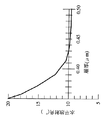
図5には、リッジストライプ形状の外部における上部クラッド層膜厚dと水平放射角との相関を示す。水平放射角特性は上部クラッド層の膜厚dが薄くなると急激に増大することがわかる。この図5から、上部クラッド層の層厚dが0.2μmより大きくなると水平放射角の広がりが抑えられることが示されている。
【0038】
本実施の形態1に示すドライエッチングによる製造方法で作製した素子では、典型的には50mAの電流でレーザー発振が観測され、放射角特性としては、垂直方向の拡がり角が24°、水平方向の拡がり角が12°の楕円率2の特性が得られたが、発振閾値は30mA〜100mA、水平方向の拡がり角は10°〜23°の範囲内にあった。また、非点隔差は1〜5μmであった。
【0039】
また、本実施の形態ではGaInN層を活性層に、GaAlNをクラッド層に使用した青色発光の半導体レーザ素子の例を示したが、この組み合わせに限らず、GaInN活性層/GaNクラッド層やGaN活性層/GaAlNクラッド層、あるいはレーザ発振が可能な組み合わせであればGaAlInN系の四元系化合物の組み合わせでも構わない。
【0040】
(実施の形態2)
図3に、リッジストライプ形状を形成するのに、選択成長法によって作製された青色発光の化合物半導体レーザ素子を示す。図1と同一部材には同一符号を付す。符号21aはp型GaAlN上部クラッド層、21bは選択成長させたp型GaAlN上部クラッド層、23はSiO2保護膜である。この化合物半導体レーザ素子は、リッジストライプ形状を有し、更にリッジストライプ形状のp型GaAlN上部クラッド層の表面に保護膜が酸化硅素、酸化アルミニウムの2層からなることを特徴とする。
【0041】
次に、実施の形態2の化合物半導体レーザ素子の作製方法について説明する。
【0042】
まず、実施の形態1の図2(a)と同様の方法で作製を行う。この工程を図4(a)に示す。
【0043】
次に、実施の形態1と同様にn型GaN層3、n型GaAlN下部クラッド層4、GaInN活性層5を積層し、温度を1050℃にしてアンモニアを毎分5リットル、TMGを毎分3x10⁻⁵モル、TMAを毎分6x10⁻⁶モル及びCp2 Mgを毎分5x10⁻⁶モル流し、5分間処理することで0.2μmのMgドープしたGaAlN上部クラッド層21aを成長させる。以上の工程を図4(b)に示す。
【0044】
次に、MgドープしたGaAlN上部クラッド層21aの表面に、電子ビーム蒸着法とフォトリソグラフィー法によって幅1μmの開口部22を有したSiO2膜23を形成する。以上の工程を図4(c)に示す。
【0045】
この後、幅1μmの開口部22を有するSiO2膜23の形成された、窒化ガリウム系化合物半導体によるダブルヘテロ構造を積層したウェーハーをMOCVD装置に導入し、MOCVD装置のリアクターを水素で良く置換した後、水素およびアンモニアを流しながら温度を1050℃まで上昇させ、温度が1050℃に安定したらTMGを毎分3x10⁻⁵モル、TMAを毎分6x10⁻⁶モル、Cp2 Mgを毎分5x10⁻⁶モル、アンモニアを毎分5リットル流し、20分間処理することによって幅1μmの開口部22内に約0.8μmのMgドープしたGaAlN上部クラッド層21bを成長させる。この成長は開口部22内のみに選択的に行われるため、開口部22以外のSiO2膜23上には、半導体層は成長しない。
【0046】
次に、TMAだけの供給を止め、10分間の成長で0.5μmのMgドープしたGaNコンタクト層7を成長させる。上記のようにしてSiO2膜23以外の部分を選択的に成長させて、光導波路となるリッジストライプ形状が形成される。以上の工程終了後の断面図を図4(d)に示す。
【0047】
次に、窒素雰囲気中で約700℃の熱処理を20分間程度行い、MgドープしたGaAlN上部クラッド層21a、21b、GaNコンタクト層7を低抵抗化及びp型化する。この処理で両層の正孔濃度は約1x1018cm-3となった。
【0048】
次に、通常のフォトリソ法を用いて、リッジストライプ形状の上面以外の表面に保護膜としてAl2O3膜9を電子ビーム蒸着法により形成し、リッジストライプ形状の上面のみにAu/Ni積層膜のp側電極10を全面的に真空蒸着法によって形成する。以上の工程終了後の断面図を図4(e)に示す。選択成長のために用いたSiO2膜を残存させて、その上にAl2O3膜9を積層することによってp型GaAlN上部クラッド層の表面保護を2層構造に簡単にすることができる。
【0049】
次に、レーザ共振器のミラー面の形成を行う。Au/Ni積層膜10による電極ストライプと直交する方向にマスクとして幅500μmのSiO2膜を50μmの間隔を開けて電子ビーム蒸着する。
【0050】
次に、50μmのストライプを有するSiO2膜が形成されたウエハを反応性イオンエッチング装置に導入し、反射ミラーを形成するためにSiO2膜の開口部分のGaAlInN系半導体層をAlNバッファ層2まで、通常の反応性イオンビームエッチング法により、エッチング除去する。更に、6H−SiC基板1を研磨し、約100μmの厚みに加工し、またマスクとしたSiO2膜を除去する。
【0051】
最後に、n側電極11をSiC基板1の裏面全面に形成し、スクライビングによりチップに分割し、通常の方法にてパッケージに実装して窒化物系レーザ素子が完成する。
【0052】
上記選択成長法を用いて製造された化合物半導体レーザ素子に電流を流したところ、典型的には、40mAのしきい値電流で432nmの青色波長でのレーザー発振が観測され、放射角特性としては垂直方向の拡がり角が24°、水平方向の拡がり角が12°の楕円率2の特性が得られた。また、非点隔差は1〜5μmであった。
【0053】
本実施の形態で作製した素子では、発振しきい値は38mA〜42mA、水平方向の拡がり角は11.5°〜12.5°の範囲のばらつきであり、実施の形態1の特性と比較しリッジストライプの外側のクラッド層厚制御に優れていることが示された。MOCVD法によるGaAlNクラッド層の膜厚制御性は、φ2インチの基板面内において±2%程度であった。
【0054】
また、本実施の形態2で示す化合物半導体レーザ素子は、リッジストライプ形状の外側の上部クラッド層の保護膜が酸化アルミニウムと酸化硅素の2層になっているので、保護効果が高く、素子寿命が改善される。
【0055】
尚、本実施の形態では、基板としてn型(0001)硅素(Si)面から<1120>方向に5度オフした6H−SiC基板1を用いた例について説明したが、p−型SiC基板を用いても実現でき、この場合は実施の形態で記載した各半導体層の伝導型を逆さにする必要がある。また、オフしていない基板を用いても同様の効果が得られた。更に6H−SiCに限らず、4H−SiC基板、2H−SiC基板を用いても同等以上の効果が得られる。
【0056】
また、リッジストライプ形状は、上部クラッド層から形成する必要はなく、コンタクト層のみをリッジストライプ形状にしても、ほぼ同様の効果が得られる。
【0057】
(実施の形態3)
図6に、(実施の形態2)と同様、リッジストライプ形状を形成するのに、選択成長法を用い、絶縁性基板上に作製された青色発光の化合物半導体レーザ素子を示す。図1及び図3と同一部材には同一符号を付す。符号55は単一量子井戸構造GaInN活性層、101は絶縁性基板、102はGaNバッファ層である。この化合物半導体レーザ素子は、リッジストライプ形状を有し、更にリッジストライプ形状のp型GaAlN上部クラッド層の表面に保護膜が酸化硅素、酸化アルミニウムの2層からなることを特徴とすることは、(実施の形態2)と同様である。
【0058】
次に、実施の形態3の化合物半導体レーザ素子の作製方法について説明する。
【0059】
まず、実施の形態3の図4(a)と同様の方法で作製を行う。この工程を図7(a)に示す。
【0060】
次に、実施の形態3と同様にn型GaN層3、n型GaAlN下部クラッド層4、単一量子井戸構造GaInN活性層55(20Å)を積層し、温度を1050℃にしてアンモニアを毎分5リットル、TMGを毎分3x10⁻⁵モル、TMAを毎分6x10⁻⁶モル及びCp2 Mgを毎分5x10⁻⁶モル流し、11分間処理することで0.43μmのMgドープしたGaAlN上部クラッド層21aを成長させる。以上の工程終了後の断面図を図7(b)に示す。
【0061】
次に、MgドープしたGaAlN上部クラッド層21aの表面に、電子ビーム蒸着法とフォトリソグラフィー法によって幅1μmの開口部22を有したSiO2膜23を形成する。以上の工程終了後の断面図を図7(c)に示す。
【0062】
この後、幅1μmの開口部22を有するSiO2膜23の形成された、窒化ガリウム系化合物半導体によるダブルヘテロ構造を積層したウェーハーをMOCVD装置にし、リアクターを水素で良く置換した後、水素およびアンモニアを流しながら温度を1050℃まで上昇させ、温度が1050℃に安定したらTMGを毎分3x10⁻⁵モル、TMAを毎分6x10⁻⁶モル、Cp2 Mgを毎分5x10⁻⁶モル、アンモニアを毎分5リットル流し、20分間処理することによって幅1μmの開口部22内に約0.8μmのMgドープしたGaAlN上部クラッド層21bを成長させる。この成長は開口部22内のみに選択的に行われるため、開口部22以外のSiO2 膜23上には、半導体層は成長しない。
【0063】
次に、TMAだけの供給を止め、10分間の成長で0.5μmのMgドープしたGaNコンタクト層7を成長させる。上記のようにしてSiO2膜23以外の部分を選択的に成長させて、光導波路となるリッジストライプ形状が形成される。以上の工程終了後の断面図を図7(d)に示す。
【0064】
次に、窒素雰囲気中で約700℃の熱処理を20分間程度行い、MgドープしたGaAlN上部クラッド層21a、21b、GaNコンタクト層7を低抵抗化及びp型化する。この処理で両層の正孔濃度は約1x1018cm-3となった。
【0065】
次に、通常のフォトリソ法を用いて、ウエハ表面全面に保護膜としてAl2O3膜9を電子ビーム蒸着法により形成し、リッジストライプ形状以外の箇所のAl2O3膜9、及びSiO2膜23をストライプ状に除去し、開口部222を設ける。以上の工程終了後の断面図を図7(e)に示す。
【0066】
次に、開口部222が形成されたウエハを反応性イオンエッチング装置に導入し、n側電極を形成するためにAl2O3膜9、及びSiO2膜23の開口部分の窒化ガリウム系半導体層をn型GaN層3まで、通常の反応性イオンビームエッチング法により、エッチング除去する。以上の工程終了後の断面図を図7(f)に示す。
【0067】
次に、通常のフォトリソ法を用いて、n側電極11をn型GaN層3の表面に形成する。
【0068】
次に、通常のフォトリソ法を用いて、リッジストライプ形状の上面のみにAu/Ni積層膜のp側電極10を全面的に真空蒸着法によって形成する。
【0069】
次に、レーザ共振器のミラー面の形成を行う。Au/Ni積層膜10による電極ストライプと直交する方向にマスクとして幅500μmのSiO2膜を50μmの間隔を開けて電子ビーム蒸着する。
【0070】
次に、50μmのストライプを有するSiO2膜が形成されたウエハを反応性イオンエッチング装置に導入し、反射ミラーを形成するためにSiO2膜の開口部分の窒化ガリウム系半導体層をAlNバッファ層2まで、通常の反応性イオンビームエッチング法により、エッチング除去する。更に、絶縁性基板101を研磨し、約100μmの厚みに加工し、またマスクとしたSiO2膜を除去する。
【0071】
最後に、スクライビングによりチップに分割し、通常の方法にてパッケージに実装してレーザ素子が完成する。
【0072】
上記選択成長法を用いて製造された単一量子井戸構造活性層を持つ化合物半導体レーザ素子に電流を流したところ、典型的には、30mAのしきい値電流で420nmの青色波長でのレーザー発振が観測され、放射角特性としては垂直方向の拡がり角が20°、水平方向の拡がり角が10°の楕円率2の特性が得られた。また、非点隔差は1〜5μmであった。
【0073】
本実施の形態で作製した素子では、発振しきい値は28mA〜32mA、水平方向の拡がり角は9.5°〜10.5°の範囲のばらつきであり、実施の形態2の特性と比較して更に特性制御性に優れていることが示された。
【0074】
また、本実施の形態3で示す化合物半導体レーザ素子も、リッジストライプ形状の外側の上部クラッド層の保護膜が酸化アルミニウムと酸化硅素の2層になっているので、保護効果が高く、素子寿命が改善される。
【0075】
本実施の形態では単一量子井戸構造の活性層を備えた素子に付いて説明したが、量子井戸は複数存在する多重量子井戸構造、例えば井戸層として、厚さ20ÅのInGaN層を3層、障壁層として、厚さ30ÅのGaN層を2層、交互に積層した構造を備えた素子構造としてもよい。多重量子井戸構造の場合においては、各量子井戸層への良好なキャリヤの注入、駆動電圧の低減を考慮した場合、量子井戸の数は3以下が望ましい。
【0076】
(実施の形態4)
図9に、(実施の形態1)と同様、リッジストライプ形状を形成するのに、ドライエッチングを用い、導電性基板上に作製された単一量子井戸構造GaInN活性層を備えた青色発光の化合物半導体レーザ素子を示す。図1、図3及び図6と同一部材には同一符号を付す。
【0077】
この、実施の形態4の化合物半導体レーザ素子の作製方法は、実施の形態1と同様の方法であるが、単一量子井戸構造GaInN活性層55を積層する点のみ、実施の形態1の作製方法と異なっている。
【0078】
次に、反応性イオンエッチング装置にて、塩素を主成分とするエッチングガスでストライプ状のSiO2膜8形成部以外のMgドープしたGaN層コンタクト層7及びMgドープしたGaAlN上部クラッド層6のエッチングを行う事も同様であるが、このエッチング工程において、MgドープしたGaAlN上部クラッド層6は0.43μmを残してエッチングか完了するようにエッチング時間の調整を行った点が実施の形態1の場合とは異なる。ここで、エッチング条件としてDCバイアスを200V、RFパワー300Wとすることにより、GaN層コンタクト層7及びMgドープしたGaAlN上部クラッド層6共にエッチング速度は3000Å/分となり、エッチングは約3分25秒行った。上記条件では、DCバイアスは±50V、RFパワーは±50Wであり、エッチング速度のばらつきは±10%程度であった。
【0079】
次に、窒素雰囲気中で約700℃の熱処理も実施の形態1と同様に行った。
【0080】
更に、リッジ型ストライプの上面のAu/Ni積層膜のp側電極10の形成、レーザ共振器のミラー面の形成、n側電極11をSiC基板1の裏面全面に形成する工程も実施の形態1と同様に行った。
【0081】
最後に、スクライビングによりチップに分割し、通常の方法にてパッケージに実装してレーザ素子が完成する。
【0082】
本実施の形態4に示すドライエッチングによる製造方法で作製した素子の特性は、実施の形態3のものと同様であった。
【0083】
また、本実施の形態ではGaInN層を活性層に、GaAlNをクラッド層に使用した青色発光の半導体レーザ素子の例を示したが、この組み合わせに限らず、GaInN活性層/GaNクラッド層やGaN活性層/GaAlNクラッド層、あるいはレーザ発振が可能な組み合わせであればGaAlInN系の四元系化合物の組み合わせでも構わないことも、実施の形態1の場合と同様である。
【0084】
更に、本実施の形態でも実施の形態3と同様、単一量子井戸構造の活性層を備えた素子に付いて説明したが、量子井戸は複数存在する多重量子井戸構造を備えた素子構造としてもよく、多重量子井戸構造の場合においては、各量子井戸層への良好なキャリヤの注入、駆動電圧の低減を考慮した場合、量子井戸の数は3以下が望ましい事も、実施の形態3の場合と同様である。
【0085】
【発明の効果】
本実施の形態に示したようなリッジストライプ構造を持つ窒化ガリウム系の化合物半導体レーザ素子は、従来の化合物半導体レーザ素子のようにエッチングのばらつきによる電流注入不良等を発生させることが少なく、また発振しきい値が低く、非点隔差が小さくできた。
【0086】
また、本発明による化合物半導体レーザのリッジストライプ形状はドライエッチング方法によっても、選択成長方法によっても作製できる。特に、選択成長方法を用いた場合には、リッジストライプ形状の外部の上部クラッド層の膜厚制御性に優れており、素子のばらつきが改善される。また、コンタクト層と上部クラッド層の界面が存在する側面に保護層を設けることによって、電流注入経路の劣化を防止でき、さらに上部クラッド層の保護膜を2層にすることで、半導体レーザ素子の保護効果が高く、素子寿命が改善される。
【図面の簡単な説明】
【図1】本発明の実施の形態1に示すリッジストライプ形状を有する窒化ガリウム系半導体レーザ素子の断面図である。
【図2】実施の形態1に示すリッジストライプ形状を有する窒化ガリウム系半導体レーザ素子の作製行程を示す図である。
【図3】実施の形態2に示すリッジストライプ形状を有する窒化ガリウム系半導体レーザ素子の断面図である。
【図4】実施の形態2に示すリッジストライプ形状を有する窒化ガリウム系半導体レーザ素子の作製行程を示す図である。
【図5】リッジストライプ形状の外側の上部クラッド層厚と水平放射角の関係を示す図である。
【図6】実施の形態3に示すリッジストライプ形状を有する窒化ガリウム系半導体レーザ素子の断面図である。
【図7】実施の形態3に示すリッジストライプ形状を有する窒化ガリウム系半導体レーザ素子の作製行程を示す図である。
【図8】単一量子井戸活性層構造を持つ素子におけるリッジストライプ形状の外側の上部クラッド層厚と水平放射角の関係を示す図である。
【図9】実施の形態4に示すリッジストライプ形状を有する窒化ガリウム系半導体レーザ素子の断面図である。
【図10】従来の電極ストライプ構造を有する半導体レーザ素子の断面図である。
【図11】従来の内部電流狭窄構造を有する半導体レーザ素子の断面図である。
【符号の説明】
1 6H−SiC基板
101 絶縁性基板
2 AlNバッファ層
102 GaNバッファ層
3 n型GaN層
4 n型GaAlN下部クラッド層
5 InGaN活性層
55 単一量子井戸構造InGaN活性層
6 p型GaAlN上部クラッド層
7 p型GaNコンタクト層
8 SiO2膜
9 Al2O3保護膜
10 p側電極
11 n側電極
21a p型GaAlN上部クラッド層
21b 選択成長されたp型GaAlN上部クラッド層
22 開口部
222 開口部
23 SiO2膜[0001]
BACKGROUND OF THE INVENTION
The present invention relates to a gallium nitride based semiconductor laser device and a manufacturing method thereof.
[0002]
[Prior art]
Gallium nitride-based compound semiconductors are wide-gap semiconductors and have a direct transition type band structure, and thus are expected to be applied to light-emitting elements having emission wavelengths from blue to ultraviolet.
[0003]
Among these applications, double hetero-type light emitting diodes using GaInN as an active layer and GaAlN as a cladding layer have been put into practical use, and are being actively developed for practical use of semiconductor laser elements. Such a semiconductor laser device is manufactured using a sapphire or SiC substrate by a metal organic chemical vapor deposition method (hereinafter referred to as MOCVD method) or a molecular beam epitaxial method (hereinafter referred to as MBE method). Schematic diagrams of a compound semiconductor laser device manufactured conventionally are shown in FIGS.
[0004]
In the compound semiconductor laser device shown in FIG. 10, a
[0005]
In the semiconductor laser device shown in FIG. 11, a
[0006]
[Problems to be solved by the invention]
However, the above-described conventional compound semiconductor laser device and manufacturing method have the following problems. In the compound semiconductor laser device having the electrode stripe structure as shown in FIG. 10, since the current spreading in the horizontal direction in the
[0007]
On the other hand, in the case of a compound semiconductor laser device having an internal current confinement structure as shown in FIG. 11, the above-mentioned problem is solved. That is, the efficiency of current injection into the active layer 154 is good, the oscillation threshold value can be lowered, and an optical waveguide having a horizontal refractive index profile is built, so that the horizontal wavefront is small in bending and the astigmatic difference is small. Since it is as small as several μm and good focusing characteristics are obtained, it is suitable as a light source for optical disk pickups. Therefore, it is generally widely used in AlGaAs and AlGaInP infrared to red light emitting semiconductor lasers. It is well known.
[0008]
However, no suitable chemical etchant has been found for gallium nitride-based materials, and the current blocking layer necessary to fabricate the internal current confinement structure can be removed by wet etching to about 0.5 μm to 1 μm. It takes several tens of hours or more, and it is practically impossible to manufacture a compound semiconductor laser device having a structure as shown in FIG.
[0009]
Further, when the dry etching method is used for a gallium nitride-based material, a practical etching of several thousand liters per minute is possible, but the variation in the dry etching rate within the wafer surface is ± 25. As large as about%. Therefore, in the nitride compound semiconductor laser device having a standard structure as shown in FIG. 11 in which the thickness of the
[0010]
An object of the present invention is to manufacture a highly efficient gallium nitride compound semiconductor laser device having an optical waveguide structure having a refractive index distribution in the horizontal direction by solving the above problems, and a high yield gallium nitride compound semiconductor laser device Is to provide a method.
[0011]
[Means for Solving the Problems]
In the nitride semiconductor laser device according to the present invention, a first conductive type lower cladding layer, an active layer, and a second conductive type upper cladding layer are stacked in this order on a substrate. x Al y In 1-xy In a nitride semiconductor laser device made of N (0 <x ≦ 1, 0 ≦ y <1, X + Y ≦ 1), the second conductive type upper cladding layer has a ridge stripe shape extending in the cavity direction. It is characterized by.
[0012]
In the nitride semiconductor laser device of the present invention, the substrate is a first conductivity type semiconductor substrate.
[0013]
In the nitride-based semiconductor laser device of the present invention, the substrate is an insulating substrate.
[0014]
The nitride-based semiconductor laser device of the present invention is characterized in that a protective layer is provided on the surface of the ridge stripe-shaped second conductive type upper cladding layer.
[0015]
In the nitride semiconductor laser device according to the present invention, the protective film is composed of two layers of aluminum oxide and silicon oxide.
[0016]
In the nitride semiconductor laser device of the present invention, the active layer has a quantum well structure.
[0017]
The nitride semiconductor laser device according to the present invention is characterized in that a dry etching method is used to form the ridge stripe shape.
[0018]
The nitride semiconductor laser device according to the present invention is characterized in that a selective growth method is used to form the ridge stripe shape.
[0019]
DETAILED DESCRIPTION OF THE INVENTION
(Embodiment 1)
As an embodiment according to the present invention, a method of manufacturing a compound semiconductor laser device having a double heterojunction having a GaInN active layer / GaAlN cladding layer on a SiC substrate and a ridge guide structure by using dry etching will be described. .
[0020]
The structure of a gallium nitride based semiconductor laser device according to the present invention is shown in FIG.
[0021]
The semiconductor laser element shown in FIG. 1 is characterized in that the upper clad layer forms a ridge stripe shape.
[0022]
FIG. 2 shows a cross-sectional view of a manufacturing process of a gallium nitride compound semiconductor laser according to the present invention. First, the damaged layer on the surface was removed by subjecting the 6H—
[0023]
Next, when the substrate temperature is lowered to 1050 ° C. and stabilized at 1050 ° C., trimethylaluminum (hereinafter referred to as TMA) is 3 × 10 3 per minute. -Five An
[0024]
Next, trimethyl gallium (hereinafter referred to as TMG) is 3 × 10 5 per minute. -Five The n-
[0025]
Next, in addition to ammonia and TMG, TMA is 6 × 10 / min. -6 A n-type GaAlN lower clad
[0026]
Next, the supply of TMG, TMA, and silane gas is stopped and the temperature is lowered to 800 ° C. When the temperature is stabilized at 800 ° C., TMG and trimethylindium (hereinafter referred to as TMI) are 4 × 10 4 per minute. -Four The GaInN
[0027]
Next, the supply of TMG and TMI is stopped, and the temperature is raised to 1050 ° C. again. When the temperature is stabilized at 1050 ° C., Cp as a doping material for TMG, TMA and p-type 2 5 x 10 Mg (cyclopentadienyl magnesium) per minute -6 By flowing in a molar state and treating for 25 minutes, an approximately 1 μm Mg-doped GaAlN
[0028]
Next, the supply of only TMA is stopped, and a 300 nm Mg-doped
[0029]
On the Mg-doped
[0030]
Next, in a reactive ion etching apparatus, striped SiO with an etching gas mainly composed of chlorine. 2 Etching of the Mg-doped GaN
[0031]
Next, a heat treatment at about 700 ° C. is performed in a nitrogen atmosphere for about 20 minutes, and the Mg-doped GaAlN
[0032]
Next, Al as a protective film on the side surface of the ridge stripe shape 2 O Three A film 9 is formed by an electron beam evaporation method, and then a stripe-shaped SiO having a width of 1 μm. 2 After removing the film 8 with hydrofluoric acid, washing with sufficient water and drying, the p-
[0033]
Next, the mirror surface of the laser resonator is formed. SiO having a width of 500 μm as a mask in a direction perpendicular to the electrode stripe by the Au / Ni laminated
[0034]
Next, SiO having a stripe of 50 μm 2 The wafer on which the film is formed is introduced into a reactive ion etching apparatus, and SiO is formed to form a reflection mirror. 2 The gallium nitride-based semiconductor layer in the opening of the film is removed by etching up to the
[0035]
Next, n-
[0036]
Finally, it is divided into chips by scribing and mounted on a package by a normal method to complete the laser element.
[0037]
FIG. 5 shows the correlation between the upper cladding layer thickness d outside the ridge stripe shape and the horizontal radiation angle. It can be seen that the horizontal radiation angle characteristic increases rapidly as the thickness d of the upper cladding layer decreases. FIG. 5 shows that the spread of the horizontal radiation angle can be suppressed when the thickness d of the upper cladding layer is larger than 0.2 μm.
[0038]
In an element manufactured by the manufacturing method using dry etching shown in the first embodiment, laser oscillation is typically observed at a current of 50 mA, and the radiation angle characteristics include a vertical divergence angle of 24 ° and a horizontal direction. The characteristic of
[0039]
In this embodiment, an example of a blue light emitting semiconductor laser element using a GaInN layer as an active layer and GaAlN as a cladding layer is shown. However, the present invention is not limited to this combination, and the GaInN active layer / GaN cladding layer or GaN active layer A layer / GaAlN cladding layer, or a combination of GaAlInN-based quaternary compounds as long as the combination is capable of laser oscillation.
[0040]
(Embodiment 2)
FIG. 3 shows a blue-emitting compound semiconductor laser device manufactured by a selective growth method to form a ridge stripe shape. The same members as those in FIG.
[0041]
Next, a method for manufacturing the compound semiconductor laser device of the second embodiment will be described.
[0042]
First, fabrication is performed in the same manner as in FIG. This process is shown in FIG.
[0043]
Next, as in the first embodiment, an n-
[0044]
Next, on the surface of the Mg-doped GaAlN
[0045]
Thereafter, SiO having an
[0046]
Next, the supply of only TMA is stopped, and a 0.5 μm Mg-doped
[0047]
Next, a heat treatment at about 700 ° C. is performed for about 20 minutes in a nitrogen atmosphere, and the Mg-doped GaAlN upper cladding layers 21a and 21b and the
[0048]
Next, using a normal photolithography method, a protective film is formed on the surface other than the top surface of the ridge stripe shape. 2 O Three The
[0049]
Next, the mirror surface of the laser resonator is formed. SiO having a width of 500 μm as a mask in a direction perpendicular to the electrode stripe by the Au / Ni laminated
[0050]
Next, SiO having a stripe of 50 μm 2 The wafer on which the film is formed is introduced into a reactive ion etching apparatus, and SiO is formed to form a reflection mirror. 2 The GaAlInN-based semiconductor layer in the opening of the film is removed by etching up to the
[0051]
Finally, an n-
[0052]
When a current was passed through the compound semiconductor laser device manufactured using the selective growth method, laser oscillation at a blue wavelength of 432 nm was typically observed with a threshold current of 40 mA, and the radiation angle characteristics were A characteristic of
[0053]
In the element manufactured in this embodiment, the oscillation threshold is 38 mA to 42 mA, and the horizontal divergence angle is in the range of 11.5 ° to 12.5 °. Compared with the characteristics of the first embodiment, It was shown that the cladding layer thickness control outside the ridge stripe is excellent. The film thickness controllability of the GaAlN cladding layer by the MOCVD method was about ± 2% in the φ2 inch substrate surface.
[0054]
In the compound semiconductor laser device shown in the second embodiment, the protective film of the upper clad layer outside the ridge stripe has two layers of aluminum oxide and silicon oxide, so that the protective effect is high and the device life is long. Improved.
[0055]
In this embodiment, the example in which the 6H—
[0056]
The ridge stripe shape does not need to be formed from the upper clad layer, and substantially the same effect can be obtained even if only the contact layer is formed into the ridge stripe shape.
[0057]
(Embodiment 3)
FIG. 6 shows a blue-emitting compound semiconductor laser device formed on an insulating substrate using a selective growth method to form a ridge stripe shape as in (Embodiment 2). The same members as those in FIGS. 1 and 3 are denoted by the same reference numerals.
[0058]
Next, a method for manufacturing the compound semiconductor laser device of the third embodiment will be described.
[0059]
First, fabrication is performed in the same manner as in FIG. This process is shown in FIG.
[0060]
Next, similarly to the third embodiment, an n-
[0061]
Next, SiO having an
[0062]
Thereafter, SiO having an
[0063]
Next, the supply of only TMA is stopped, and a 0.5 μm Mg-doped
[0064]
Next, a heat treatment at about 700 ° C. is performed for about 20 minutes in a nitrogen atmosphere, and the Mg-doped GaAlN upper cladding layers 21a and 21b and the
[0065]
Next, using a normal photolithography method, Al is applied as a protective film over the entire wafer surface. 2 O Three The
[0066]
Next, the wafer having the opening 222 formed therein is introduced into a reactive ion etching apparatus, and Al is formed to form an n-side electrode. 2 O Three Film 9 and SiO 2 The gallium nitride based semiconductor layer in the opening of the
[0067]
Next, the n-
[0068]
Next, the p-
[0069]
Next, the mirror surface of the laser resonator is formed. SiO having a width of 500 μm as a mask in a direction perpendicular to the electrode stripe by the Au / Ni laminated
[0070]
Next, SiO having a stripe of 50 μm 2 The wafer on which the film is formed is introduced into a reactive ion etching apparatus, and SiO is formed to form a reflection mirror. 2 The gallium nitride-based semiconductor layer in the opening of the film is removed by etching up to the
[0071]
Finally, it is divided into chips by scribing and mounted on a package by a normal method to complete the laser element.
[0072]
When a current is passed through a compound semiconductor laser device having a single quantum well structure active layer manufactured using the selective growth method, laser oscillation at a blue wavelength of 420 nm is typically performed with a threshold current of 30 mA. As a radiation angle characteristic, an
[0073]
In the element manufactured in this embodiment, the oscillation threshold is 28 mA to 32 mA, and the horizontal divergence angle is in the range of 9.5 ° to 10.5 °. Compared with the characteristics of the second embodiment. It was also shown that the property controllability is further excellent.
[0074]
The compound semiconductor laser device shown in the third embodiment also has a high protective effect and a long device life because the protective film of the upper cladding layer on the outer side of the ridge stripe shape is composed of two layers of aluminum oxide and silicon oxide. Improved.
[0075]
In the present embodiment, an element having an active layer having a single quantum well structure has been described. However, a quantum well has a plurality of multiple quantum well structures, for example, three InGaN layers having a thickness of 20 mm as well layers, The barrier layer may be an element structure having a structure in which two GaN layers having a thickness of 30 mm are alternately stacked. In the case of a multiple quantum well structure, the number of quantum wells is desirably 3 or less in consideration of good carrier injection into each quantum well layer and reduction in driving voltage.
[0076]
(Embodiment 4)
In FIG. 9, as in (Embodiment 1), a blue light emitting compound having a single quantum well structure GaInN active layer formed on a conductive substrate using dry etching to form a ridge stripe shape. 1 shows a semiconductor laser element. The same members as those in FIG. 1, FIG. 3 and FIG.
[0077]
The manufacturing method of the compound semiconductor laser device of the fourth embodiment is the same as that of the first embodiment, but the manufacturing method of the first embodiment is only in that the single quantum well structure GaInN
[0078]
Next, in a reactive ion etching apparatus, striped SiO with an etching gas mainly composed of chlorine. 2 Etching the Mg-doped GaN
[0079]
Next, heat treatment at about 700 ° C. in a nitrogen atmosphere was performed in the same manner as in the first embodiment.
[0080]
Further, the steps of forming the p-
[0081]
Finally, it is divided into chips by scribing and mounted on a package by a normal method to complete the laser element.
[0082]
The characteristics of the element manufactured by the dry etching manufacturing method shown in the fourth embodiment were the same as those in the third embodiment.
[0083]
In this embodiment, an example of a blue light emitting semiconductor laser element using a GaInN layer as an active layer and GaAlN as a cladding layer is shown. However, the present invention is not limited to this combination, and a GaInN active layer / GaN cladding layer or GaN active layer is used. As in the case of the first embodiment, a combination of a layer / GaAlN cladding layer or a combination of GaAlInN-based quaternary compounds may be used as long as the combination is capable of laser oscillation.
[0084]
Further, in the present embodiment as well as the third embodiment, the description has been made on the element having the active layer having the single quantum well structure. However, the element structure having the multiple quantum well structure in which a plurality of quantum wells exist may be used. In the case of a multiple quantum well structure, the number of quantum wells is preferably 3 or less in consideration of good carrier injection into each quantum well layer and reduction in driving voltage. It is the same.
[0085]
【The invention's effect】
The gallium nitride compound semiconductor laser device having a ridge stripe structure as shown in the present embodiment is less likely to cause current injection failure due to etching variations and oscillates unlike the conventional compound semiconductor laser device. The threshold value was low and the astigmatic difference was reduced.
[0086]
Further, the ridge stripe shape of the compound semiconductor laser according to the present invention can be produced by a dry etching method or a selective growth method. In particular, when the selective growth method is used, the film thickness controllability of the outer upper cladding layer in the ridge stripe shape is excellent, and the variation of the elements is improved. In addition, by providing a protective layer on the side surface where the interface between the contact layer and the upper cladding layer exists, it is possible to prevent the current injection path from deteriorating. Further, by forming the protective film of the upper cladding layer into two layers, The protective effect is high and the device life is improved.
[Brief description of the drawings]
FIG. 1 is a cross-sectional view of a gallium nitride based semiconductor laser device having a ridge stripe shape according to a first embodiment of the present invention.
FIG. 2 is a diagram showing a manufacturing process of the gallium nitride based semiconductor laser device having the ridge stripe shape shown in the first embodiment.
FIG. 3 is a cross-sectional view of a gallium nitride based semiconductor laser device having a ridge stripe shape shown in the second embodiment.
4 is a diagram showing a manufacturing process of a gallium nitride based semiconductor laser device having a ridge stripe shape shown in
FIG. 5 is a diagram showing the relationship between the outer upper cladding layer thickness of the ridge stripe shape and the horizontal radiation angle.
6 is a cross-sectional view of a gallium nitride based semiconductor laser device having a ridge stripe shape shown in
7 is a diagram showing a manufacturing process of a gallium nitride based semiconductor laser device having a ridge stripe shape shown in
FIG. 8 is a diagram showing the relationship between the thickness of the upper cladding layer outside the ridge stripe shape and the horizontal radiation angle in an element having a single quantum well active layer structure.
FIG. 9 is a cross-sectional view of a gallium nitride based semiconductor laser device having a ridge stripe shape shown in a fourth embodiment.
FIG. 10 is a sectional view of a semiconductor laser device having a conventional electrode stripe structure.
FIG. 11 is a cross-sectional view of a semiconductor laser device having a conventional internal current confinement structure.
[Explanation of symbols]
16H-SiC substrate
101 Insulating substrate
2 AlN buffer layer
102 GaN buffer layer
3 n-type GaN layer
4 n-type GaAlN lower cladding layer
5 InGaN active layer
55 Single Quantum Well Structure InGaN Active Layer
6 p-type GaAlN upper cladding layer
7 p-type GaN contact layer
8 SiO 2 film
9 Al 2 O Three Protective film
10 p-side electrode
11 n-side electrode
21a p-type GaAlN upper cladding layer
21b selectively grown p-type GaAlN upper cladding layer
22 opening
222 opening
23 SiO 2 film
Claims (4)
基板上に、下部クラッド層と、活性層と、上部クラッド層とをこの順に形成する工程と、
前記上部クラッド層上に開口部を有する保護膜を形成する工程と、
前記上部クラッド層とコンタクト層とを前記保護膜の開口部から選択成長し、リッジストライプを形成する工程と、
前記リッジストライプの上面に接する電極を形成する工程を有し、
前記保護膜が前記上部クラッド層表面に残存されることを特徴とする窒化物系半導体レーザ素子の製造方法。A Ga x Al y In 1-x -y N (0 <x ≦ 1,0 ≦ y <1, x + y ≦ 1) nitride production method of a semiconductor laser device made of,
Forming a lower cladding layer, an active layer, and an upper cladding layer in this order on the substrate;
Forming a protective film having an opening on the upper cladding layer;
Selectively growing the upper cladding layer and the contact layer from the opening of the protective film to form a ridge stripe;
Forming an electrode in contact with the upper surface of the ridge stripe;
The process for producing a nitride semiconductor laser device, wherein the protective film is left on the upper cladding layer surface.
Priority Applications (1)
| Application Number | Priority Date | Filing Date | Title |
|---|---|---|---|
| JP3592797A JP3878707B2 (en) | 1996-02-21 | 1997-02-20 | Nitride semiconductor laser device manufacturing method |
Applications Claiming Priority (3)
| Application Number | Priority Date | Filing Date | Title |
|---|---|---|---|
| JP3366096 | 1996-02-21 | ||
| JP8-33660 | 1996-02-21 | ||
| JP3592797A JP3878707B2 (en) | 1996-02-21 | 1997-02-20 | Nitride semiconductor laser device manufacturing method |
Related Child Applications (2)
| Application Number | Title | Priority Date | Filing Date |
|---|---|---|---|
| JP2001044408A Division JP2001257433A (en) | 1996-02-21 | 2001-02-21 | Nitride based semiconductor laser device |
| JP2001044407A Division JP4118025B2 (en) | 1996-02-21 | 2001-02-21 | Gallium nitride semiconductor laser device |
Publications (2)
| Publication Number | Publication Date |
|---|---|
| JPH09289358A JPH09289358A (en) | 1997-11-04 |
| JP3878707B2 true JP3878707B2 (en) | 2007-02-07 |
Family
ID=26372395
Family Applications (1)
| Application Number | Title | Priority Date | Filing Date |
|---|---|---|---|
| JP3592797A Expired - Fee Related JP3878707B2 (en) | 1996-02-21 | 1997-02-20 | Nitride semiconductor laser device manufacturing method |
Country Status (1)
| Country | Link |
|---|---|
| JP (1) | JP3878707B2 (en) |
Families Citing this family (5)
| Publication number | Priority date | Publication date | Assignee | Title |
|---|---|---|---|---|
| JP4639571B2 (en) * | 1998-02-17 | 2011-02-23 | 日亜化学工業株式会社 | Nitride semiconductor laser device and manufacturing method thereof |
| US6618416B1 (en) | 1998-10-07 | 2003-09-09 | Sharp Kabushiki Kaisha | Semiconductor laser |
| JP3936109B2 (en) | 1999-04-26 | 2007-06-27 | 富士通株式会社 | Semiconductor light emitting device and manufacturing method thereof |
| JP3723434B2 (en) * | 1999-09-24 | 2005-12-07 | 三洋電機株式会社 | Semiconductor light emitting device |
| JP5442229B2 (en) * | 2008-09-04 | 2014-03-12 | ローム株式会社 | Method of manufacturing nitride semiconductor device |
-
1997
- 1997-02-20 JP JP3592797A patent/JP3878707B2/en not_active Expired - Fee Related
Also Published As
| Publication number | Publication date |
|---|---|
| JPH09289358A (en) | 1997-11-04 |
Similar Documents
| Publication | Publication Date | Title |
|---|---|---|
| JP3594826B2 (en) | Nitride semiconductor light emitting device and method of manufacturing the same | |
| JP4166885B2 (en) | Optical semiconductor device and manufacturing method thereof | |
| KR100763827B1 (en) | Semiconductor laser device, and method of manufacturing the same | |
| US7015053B2 (en) | Nitride semiconductor laser device | |
| JP5036617B2 (en) | Nitride semiconductor light emitting device | |
| US20040041156A1 (en) | Nitride semiconductor light emitting element and production thereof | |
| JP2009158893A (en) | Semiconductor light-emitting element and manufacturing method therefor | |
| US5966396A (en) | Gallium nitride-based compound semiconductor laser and method of manufacturing the same | |
| JP3716974B2 (en) | Semiconductor laser device and manufacturing method thereof | |
| JP4967657B2 (en) | Group III nitride semiconductor optical device and manufacturing method thereof | |
| JP4291960B2 (en) | Nitride semiconductor device | |
| JP2002314203A (en) | Group iii nitride semiconductor laser and its manufacturing method | |
| JP4991025B2 (en) | Nitride semiconductor laser device | |
| JP4162560B2 (en) | Nitride semiconductor light emitting device | |
| JP2002324913A (en) | Iii nitride semiconductor and method of manufacturing the same, and semiconductor device and method of manufacturing the same | |
| JP3878707B2 (en) | Nitride semiconductor laser device manufacturing method | |
| JPH1093198A (en) | Gallium nitride compound semiconductor laser and its manufacture thereof | |
| JP4683730B2 (en) | Nitride semiconductor light emitting device and apparatus including the same | |
| JP4118025B2 (en) | Gallium nitride semiconductor laser device | |
| JP4045792B2 (en) | Nitride semiconductor laser device | |
| JP4304883B2 (en) | Nitride semiconductor laser diode and manufacturing method thereof | |
| JP2000183466A (en) | Compound semiconductor laser and its manufacturing method | |
| JP3984200B2 (en) | Method of manufacturing gallium nitride compound semiconductor laser | |
| JP4955195B2 (en) | Nitride semiconductor device | |
| JP3963233B2 (en) | Gallium nitride compound semiconductor light emitting device and method for manufacturing the same |
Legal Events
| Date | Code | Title | Description |
|---|---|---|---|
| A621 | Written request for application examination |
Free format text: JAPANESE INTERMEDIATE CODE: A621 Effective date: 20040219 |
|
| RD03 | Notification of appointment of power of attorney |
Free format text: JAPANESE INTERMEDIATE CODE: A7423 Effective date: 20040219 |
|
| A521 | Written amendment |
Free format text: JAPANESE INTERMEDIATE CODE: A523 Effective date: 20040324 |
|
| A131 | Notification of reasons for refusal |
Free format text: JAPANESE INTERMEDIATE CODE: A131 Effective date: 20050208 |
|
| A521 | Written amendment |
Free format text: JAPANESE INTERMEDIATE CODE: A523 Effective date: 20050411 |
|
| A02 | Decision of refusal |
Free format text: JAPANESE INTERMEDIATE CODE: A02 Effective date: 20051206 |
|
| A521 | Written amendment |
Free format text: JAPANESE INTERMEDIATE CODE: A523 Effective date: 20060201 |
|
| A911 | Transfer of reconsideration by examiner before appeal (zenchi) |
Free format text: JAPANESE INTERMEDIATE CODE: A911 Effective date: 20060320 |
|
| A131 | Notification of reasons for refusal |
Free format text: JAPANESE INTERMEDIATE CODE: A131 Effective date: 20060418 |
|
| A521 | Written amendment |
Free format text: JAPANESE INTERMEDIATE CODE: A523 Effective date: 20060525 |
|
| TRDD | Decision of grant or rejection written | ||
| A01 | Written decision to grant a patent or to grant a registration (utility model) |
Free format text: JAPANESE INTERMEDIATE CODE: A01 Effective date: 20061031 |
|
| A61 | First payment of annual fees (during grant procedure) |
Free format text: JAPANESE INTERMEDIATE CODE: A61 Effective date: 20061106 |
|
| R150 | Certificate of patent (=grant) or registration of utility model |
Free format text: JAPANESE INTERMEDIATE CODE: R150 |
|
| FPAY | Renewal fee payment (prs date is renewal date of database) |
Free format text: PAYMENT UNTIL: 20091110 Year of fee payment: 3 |
|
| FPAY | Renewal fee payment (prs date is renewal date of database) |
Free format text: PAYMENT UNTIL: 20101110 Year of fee payment: 4 |
|
| FPAY | Renewal fee payment (prs date is renewal date of database) |
Free format text: PAYMENT UNTIL: 20111110 Year of fee payment: 5 |
|
| FPAY | Renewal fee payment (prs date is renewal date of database) |
Free format text: PAYMENT UNTIL: 20111110 Year of fee payment: 5 |
|
| FPAY | Renewal fee payment (prs date is renewal date of database) |
Free format text: PAYMENT UNTIL: 20121110 Year of fee payment: 6 |
|
| FPAY | Renewal fee payment (prs date is renewal date of database) |
Free format text: PAYMENT UNTIL: 20121110 Year of fee payment: 6 |
|
| FPAY | Renewal fee payment (prs date is renewal date of database) |
Free format text: PAYMENT UNTIL: 20131110 Year of fee payment: 7 |
|
| LAPS | Cancellation because of no payment of annual fees |