JP3875673B2 - Adjustable dispersion compensator with multimode fiber and switchable mode converter - Google Patents
Adjustable dispersion compensator with multimode fiber and switchable mode converter Download PDFInfo
- Publication number
- JP3875673B2 JP3875673B2 JP2003312229A JP2003312229A JP3875673B2 JP 3875673 B2 JP3875673 B2 JP 3875673B2 JP 2003312229 A JP2003312229 A JP 2003312229A JP 2003312229 A JP2003312229 A JP 2003312229A JP 3875673 B2 JP3875673 B2 JP 3875673B2
- Authority
- JP
- Japan
- Prior art keywords
- mode
- optical signal
- dispersion
- optical
- fiber
- Prior art date
- Legal status (The legal status is an assumption and is not a legal conclusion. Google has not performed a legal analysis and makes no representation as to the accuracy of the status listed.)
- Expired - Fee Related
Links
- 239000006185 dispersion Substances 0.000 title claims description 106
- 239000000835 fiber Substances 0.000 title description 63
- 230000003287 optical effect Effects 0.000 claims description 70
- 239000013307 optical fiber Substances 0.000 claims description 18
- 238000006243 chemical reaction Methods 0.000 claims description 5
- 238000009826 distribution Methods 0.000 claims description 2
- 238000004891 communication Methods 0.000 description 16
- 230000005540 biological transmission Effects 0.000 description 14
- 238000000034 method Methods 0.000 description 11
- 230000003068 static effect Effects 0.000 description 11
- 238000010586 diagram Methods 0.000 description 10
- 230000008859 change Effects 0.000 description 7
- 230000003321 amplification Effects 0.000 description 6
- 238000003199 nucleic acid amplification method Methods 0.000 description 6
- 230000008878 coupling Effects 0.000 description 5
- 238000010168 coupling process Methods 0.000 description 5
- 238000005859 coupling reaction Methods 0.000 description 5
- 230000008569 process Effects 0.000 description 5
- 230000004044 response Effects 0.000 description 5
- 230000008901 benefit Effects 0.000 description 3
- 238000013461 design Methods 0.000 description 3
- 238000001514 detection method Methods 0.000 description 3
- 238000005516 engineering process Methods 0.000 description 3
- 238000004519 manufacturing process Methods 0.000 description 3
- 239000000463 material Substances 0.000 description 3
- 230000007246 mechanism Effects 0.000 description 3
- 230000009471 action Effects 0.000 description 2
- 238000013459 approach Methods 0.000 description 2
- 238000012937 correction Methods 0.000 description 2
- 230000005284 excitation Effects 0.000 description 2
- 229910052751 metal Inorganic materials 0.000 description 2
- 239000002184 metal Substances 0.000 description 2
- 238000005192 partition Methods 0.000 description 2
- 230000000737 periodic effect Effects 0.000 description 2
- 230000000704 physical effect Effects 0.000 description 2
- 230000000644 propagated effect Effects 0.000 description 2
- 239000000758 substrate Substances 0.000 description 2
- 230000002238 attenuated effect Effects 0.000 description 1
- 238000004364 calculation method Methods 0.000 description 1
- 238000005253 cladding Methods 0.000 description 1
- 230000006735 deficit Effects 0.000 description 1
- 230000001419 dependent effect Effects 0.000 description 1
- 230000007613 environmental effect Effects 0.000 description 1
- 230000008713 feedback mechanism Effects 0.000 description 1
- 238000010438 heat treatment Methods 0.000 description 1
- GQYHUHYESMUTHG-UHFFFAOYSA-N lithium niobate Chemical compound [Li+].[O-][Nb](=O)=O GQYHUHYESMUTHG-UHFFFAOYSA-N 0.000 description 1
- 238000012986 modification Methods 0.000 description 1
- 230000004048 modification Effects 0.000 description 1
- 239000000382 optic material Substances 0.000 description 1
- 230000001151 other effect Effects 0.000 description 1
- 230000010363 phase shift Effects 0.000 description 1
- 238000003825 pressing Methods 0.000 description 1
- 230000003595 spectral effect Effects 0.000 description 1
- 101150071238 tut1 gene Proteins 0.000 description 1
Images


Classifications
-
- G—PHYSICS
- G02—OPTICS
- G02B—OPTICAL ELEMENTS, SYSTEMS OR APPARATUS
- G02B6/00—Light guides; Structural details of arrangements comprising light guides and other optical elements, e.g. couplings
- G02B6/02—Optical fibres with cladding with or without a coating
-
- G—PHYSICS
- G02—OPTICS
- G02B—OPTICAL ELEMENTS, SYSTEMS OR APPARATUS
- G02B6/00—Light guides; Structural details of arrangements comprising light guides and other optical elements, e.g. couplings
- G02B6/24—Coupling light guides
- G02B6/26—Optical coupling means
- G02B6/28—Optical coupling means having data bus means, i.e. plural waveguides interconnected and providing an inherently bidirectional system by mixing and splitting signals
- G02B6/293—Optical coupling means having data bus means, i.e. plural waveguides interconnected and providing an inherently bidirectional system by mixing and splitting signals with wavelength selective means
- G02B6/29371—Optical coupling means having data bus means, i.e. plural waveguides interconnected and providing an inherently bidirectional system by mixing and splitting signals with wavelength selective means operating principle based on material dispersion
- G02B6/29374—Optical coupling means having data bus means, i.e. plural waveguides interconnected and providing an inherently bidirectional system by mixing and splitting signals with wavelength selective means operating principle based on material dispersion in an optical light guide
- G02B6/29376—Optical coupling means having data bus means, i.e. plural waveguides interconnected and providing an inherently bidirectional system by mixing and splitting signals with wavelength selective means operating principle based on material dispersion in an optical light guide coupling light guides for controlling wavelength dispersion, e.g. by concatenation of two light guides having different dispersion properties
- G02B6/29377—Optical coupling means having data bus means, i.e. plural waveguides interconnected and providing an inherently bidirectional system by mixing and splitting signals with wavelength selective means operating principle based on material dispersion in an optical light guide coupling light guides for controlling wavelength dispersion, e.g. by concatenation of two light guides having different dispersion properties controlling dispersion around 1550 nm, i.e. S, C, L and U bands from 1460-1675 nm
-
- H—ELECTRICITY
- H04—ELECTRIC COMMUNICATION TECHNIQUE
- H04B—TRANSMISSION
- H04B10/00—Transmission systems employing electromagnetic waves other than radio-waves, e.g. infrared, visible or ultraviolet light, or employing corpuscular radiation, e.g. quantum communication
- H04B10/25—Arrangements specific to fibre transmission
- H04B10/2507—Arrangements specific to fibre transmission for the reduction or elimination of distortion or dispersion
- H04B10/2513—Arrangements specific to fibre transmission for the reduction or elimination of distortion or dispersion due to chromatic dispersion
- H04B10/25133—Arrangements specific to fibre transmission for the reduction or elimination of distortion or dispersion due to chromatic dispersion including a lumped electrical or optical dispersion compensator
-
- G—PHYSICS
- G02—OPTICS
- G02B—OPTICAL ELEMENTS, SYSTEMS OR APPARATUS
- G02B6/00—Light guides; Structural details of arrangements comprising light guides and other optical elements, e.g. couplings
- G02B6/10—Light guides; Structural details of arrangements comprising light guides and other optical elements, e.g. couplings of the optical waveguide type
- G02B6/14—Mode converters
-
- G—PHYSICS
- G02—OPTICS
- G02B—OPTICAL ELEMENTS, SYSTEMS OR APPARATUS
- G02B6/00—Light guides; Structural details of arrangements comprising light guides and other optical elements, e.g. couplings
- G02B6/24—Coupling light guides
- G02B6/26—Optical coupling means
- G02B6/28—Optical coupling means having data bus means, i.e. plural waveguides interconnected and providing an inherently bidirectional system by mixing and splitting signals
- G02B6/293—Optical coupling means having data bus means, i.e. plural waveguides interconnected and providing an inherently bidirectional system by mixing and splitting signals with wavelength selective means
- G02B6/29379—Optical coupling means having data bus means, i.e. plural waveguides interconnected and providing an inherently bidirectional system by mixing and splitting signals with wavelength selective means characterised by the function or use of the complete device
- G02B6/29395—Optical coupling means having data bus means, i.e. plural waveguides interconnected and providing an inherently bidirectional system by mixing and splitting signals with wavelength selective means characterised by the function or use of the complete device configurable, e.g. tunable or reconfigurable
Landscapes
- Physics & Mathematics (AREA)
- Chemical & Material Sciences (AREA)
- Dispersion Chemistry (AREA)
- General Physics & Mathematics (AREA)
- Optics & Photonics (AREA)
- Engineering & Computer Science (AREA)
- Electromagnetism (AREA)
- Computer Networks & Wireless Communication (AREA)
- Signal Processing (AREA)
- Optical Communication System (AREA)
- Optical Modulation, Optical Deflection, Nonlinear Optics, Optical Demodulation, Optical Logic Elements (AREA)
- Optical Fibers, Optical Fiber Cores, And Optical Fiber Bundles (AREA)
- Light Guides In General And Applications Therefor (AREA)
Description
本発明は高速光通信システムに関し、さらに特定すると、調整可能な分散補償装置を使用した広帯域多重波長(波長分割多重−WDM)伝送媒体内の差動分散の制御に関する。 The present invention relates to high-speed optical communication systems, and more particularly to control of differential dispersion in wideband multiplexed wavelength (wavelength division multiplexing-WDM) transmission media using adjustable dispersion compensators.
分散補償装置は高速光通信システムの根本的な構成ブロックである。重要な要求項目には低損失および波長分割多重(WDM)光波システムの各波長で分散を補償する能力が含まれる。静的な分散補償に加えて、高速光通信システムは調整可能な分散補償装置(TDC)をもやはり必要とする。それらは光ファイバ伝送ライン内で分散の変化を相殺することを容易にする。この変化は環境変化(伝送ファイバおよび部品の応力あるいは温度の変化)、非線形位相シフトの変化につながるパワー変動、あるいは様々なWDMチャネルの経路長を変えるネットワークの動的再構成に起因する可能性がある(B.J.Eggletonら、J.Lightwave Tech.、18巻、1419頁(2000年)参照)。場合によっては、伝送ファイバ内の分散の統計的変動、ならびに隣り合う増幅器収納部間の伝送ファイバの長さの統計的変化から生じる可能性もある。
現在まで、いくつかの調整可能もしくは調節可能な分散補償装置が提案および示されてきた。光波信号の分散を調整するためにチャープ型ファイバ・ブラッグ・グレーティング(FBG)が広く使用されてきた。例えば、装置の分散を変えるために、線形または非線形のチャープを備えたFBGが加熱素子またはラッチ操作可能な磁気歪力によって調整される可能性がある(米国特許第6,148,127号および第6,330,383号参照)。1〜1.5nmの帯域幅にわたる約2000ps/nmの分散調整範囲がこの技術によって示された。そのような調整可能な装置の限定された帯域幅はその用途を単一のチャネル応用に制限する。WDMシステムにこの装置を使用することは信号の個別波長チャネルへのデマルチプレキシング、および各チャネルのためのFBGを主体としたTDCの使用を伴ない、極めて高コストになる。単一チャネルFBG−TDCの代替品には、3つもしくは4つのチャネルを同時に分散補償することのできる標本FBGが含まれる。これはWDMシステムで必要となる装置の数を因数3〜4で減少させるが、それでも調整可能な分散管理を導入するのにコスト高な手段であることに変わりはない。さらに、FBGを利用するすべてのTDCはビット誤り率(BER)パワー・ペナルティにつながる群遅延(GD)リップル障害に煩わされる。さらに、GDリップルは装置の帯域幅または分散に伴なって増加する。追加的な複雑さは、実際上のFBGを主体とするTDCは全通信帯域にわたる分散補償のためにメートル長さのファイが上のFBGの製造を伴なうであろうということである。そのような長いグレーティングの製造と調整は非実用的と考えられる。 To date, several adjustable or adjustable dispersion compensators have been proposed and shown. Chirped fiber Bragg gratings (FBG) have been widely used to adjust the dispersion of lightwave signals. For example, an FBG with a linear or non-linear chirp can be tuned by a heating element or a latchable magnetostrictive force to change the dispersion of the device (US Pat. Nos. 6,148,127 and 6,330,383). A dispersion tuning range of about 2000 ps / nm over a 1-1.5 nm bandwidth has been demonstrated by this technique. The limited bandwidth of such tunable devices limits its use to single channel applications. Using this device in a WDM system is extremely expensive, with the demultiplexing of signals into individual wavelength channels and the use of FBG-based TDC for each channel. Alternatives to the single channel FBG-TDC include a sample FBG that can compensate dispersion for three or four channels simultaneously. This reduces the number of devices required in the WDM system by a factor of 3-4, but it remains a costly means to introduce adjustable distributed management. Furthermore, all TDCs that utilize FBG suffer from group delay (GD) ripple impairments that lead to bit error rate (BER) power penalties. Furthermore, GD ripple increases with device bandwidth or dispersion. An additional complication is that a TDC based on a practical FBG will involve the production of the above FBG by a meter-length phi for dispersion compensation across the entire communication band. The production and adjustment of such long gratings is considered impractical.
代替技術は光学フィルタの可変位相応答を使用して分散を調整するものである。40Gb/sで500ps/nmまでの調整範囲を備えたTDCを供給するためにプレーナ型導波路に基づく全透過フィルタが示された(C.K.Madsen、Optical Fiber Conf.2002年、論文番号TUT−1およびFD−9参照)。仮想イメージ位相アレー(VIPA)装置の分散は米国特許第6,392,807号に述べられたような特別に設計された自由空間ミラーを中継することによって調整することができる。この装置は+/−800ps/nmの調整範囲を供給することが立証された(Shirasakiら、Proc.European Conf.Optical Comm.−2000、PD−2,3参照)。これらの技術の両方、ならびに光ファイバの位相応答を利用するいくつかの他の技術は波長に関して間欠的であり、その結果、それらがWDMチャネルと符合する間欠性を有するように設計される限り、すべてのチャネルに対する同時の補償を供給することができる。しかしながら、そのような装置のすべては各「通過帯域」内の波長依存性応答に煩わされる。したがって、分散と帯域幅の間の妥協が原因となってこれらの装置は高ビット速度の用途に不適切となる可能性がある。それらはまた、FBGに基づくTDCと同様にGDリップル障害に煩わされる。最後に、位相応答に基づく装置は伝送ファイバ内外の光の結合を必要とし、高損失となる。 An alternative technique is to adjust the dispersion using the variable phase response of the optical filter. An all-pass filter based on a planar waveguide has been shown to provide a TDC with a tuning range of up to 500 ps / nm at 40 Gb / s (CK Madsen, Optical Fiber Conf. 2002, paper number TUT). -1 and FD-9). The dispersion of the virtual image phase array (VIPA) device can be adjusted by relaying a specially designed free space mirror as described in US Pat. No. 6,392,807. This device has been demonstrated to provide a tuning range of +/− 800 ps / nm (see Shirasaki et al., Proc. European Conf. Optical Comm.-2000, PD-2, 3). Both of these technologies, as well as some other technologies that take advantage of the optical fiber phase response, are intermittent in terms of wavelength, so that as long as they are designed to have intermittency that matches the WDM channel, Simultaneous compensation for all channels can be provided. However, all such devices suffer from wavelength dependent responses within each “passband”. Thus, due to a compromise between dispersion and bandwidth, these devices may be unsuitable for high bit rate applications. They are also bothered by GD ripple disturbances as well as TDC based on FBG. Finally, phase response based devices require coupling of light inside and outside the transmission fiber, resulting in high loss.
したがって、分散補償ファイバ(DCF)あるいは静的分散補償に一般的に使用される高次モード分散補償モジュール(HOM−DCM)と同様の光学性能を備えた調整可能もしくは調節可能な分散を提供することのできる装置の必要性が存在する。望ましい特性は低損失、低マルチパス干渉、および無視できるGDリップルであって、最も重要なものは波長連続性の応答である。 Accordingly, providing adjustable or tunable dispersion with optical performance similar to dispersion compensating fiber (DCF) or higher order mode dispersion compensation module (HOM-DCM) commonly used for static dispersion compensation There is a need for a device that can be used. Desirable characteristics are low loss, low multipath interference, and negligible GD ripple, the most important being the response of wavelength continuity.
本発明は、複数モード・ファイバの各空間的モードが異なるモードの分散を有することを実現することに基づく。したがって、そのようなファイバ内で異なる空間的モードを進む光は、伝搬モードおよび使用されるファイバの長さに応じて異なる量の分散を蓄積するであろう。この実現はこの概念を導入する新式の装置構造につながる。基礎的装置構造は、基本モードならびに1つまたは複数の高次モード(HOM)をサポートする2つ以上の光ファイバ区画を有する。この特性を備えた光ファイバはしばしば複数モード・ファイバと称される。複数モード・ファイバは切り換え可能な空間モード変換器(MC)によって互いに接続される。空間モード変換器は、その最も一般的形式では、1つの入来空間モードを別のものに変換する。切り換え可能なモード変換器は或る状態でモード変換を実行するが、他の状態ではいかなる変換もせずに光を通過させることはない。このMCは、長周期ファイバ・グレーティング(LPG)、結合された導波路装置、自由空間位相遅延素子、または微小電子機械(MEMs)に基づくルータとスイッチを備えて製造される可能性がある。最も一般的な形式では、MCは、いかなる入来空間モードもHOMファイバ内でいずれか1つの他の導波モードへと変換するように組み立てられる。切り換えは、歪力、温度、電子−光学もしくは非線形光学効果、あるいはMC作製に使用される光学材料内の屈折率もしくは物理的経路長を変えるようにはたらくいずれかの他の物理的効果によって達成される。付け加えると、MEMsに基づくMCのケースでは、HOMファイバのいかなるモードもそれによってサポートされるいずれか1つの他のモードへと変換するようにはたらく機械的経路決定作用によって切り換えが導入される。 The present invention is based on realizing that each spatial mode of a multimode fiber has a different mode dispersion. Thus, light traveling in different spatial modes within such a fiber will accumulate different amounts of dispersion depending on the propagation mode and the length of fiber used. This realization leads to a new device structure that introduces this concept. The basic device structure has two or more fiber optic sections that support a fundamental mode as well as one or more higher order modes (HOMs). Optical fibers with this characteristic are often referred to as multimode fibers. The multimode fibers are connected to each other by a switchable spatial mode converter (MC). A spatial mode converter, in its most general form, converts one incoming spatial mode to another. A switchable mode converter performs mode conversion in some states, but does not pass light without any conversion in other states. This MC may be manufactured with routers and switches based on long period fiber gratings (LPG), coupled waveguide devices, free space phase delay elements, or microelectromechanical machines (MEMs). In the most common form, the MC is assembled to convert any incoming spatial mode into any one other guided mode in the HOM fiber. Switching is accomplished by strain, temperature, electro-optic or nonlinear optical effects, or any other physical effect that serves to change the refractive index or physical path length in the optical material used to make the MC. The In addition, in the case of MC based on MEMs, switching is introduced by a mechanical routing action that serves to convert any mode of the HOM fiber to any one other mode supported by it.
さらに特定すると、調節可能な高次モード特性(これ以降はAHOMと称する)を備えた分散補償装置(DC)は、長さNのファイバおよびそれらを互いに接続し、かつ入力部と出力部でそれぞれ伝送ファイバに接続するN+1個のMCで構成される。N+1個のMCの切り換え状態の各組み合わせは光波信号によってとられる独自の経路に対応するであろう。これは、各MCの切り換え状態に応じて、ファイバの2つ以上の空間モードのうちの1つを信号が進むからである。したがって、MC群に関する切り換え状態の様々な置き換えは信号によって蓄積される分散値の多様性につながる。言い換えると、入来光波信号について装置が生じさせる分散の量はN+1個のMCのうちの1つまたは複数の切り換え状態を変えることによって単純に変えることができる。 More specifically, a dispersion compensator (DC) with adjustable higher-order mode characteristics (hereinafter referred to as AHOM) connects fibers of length N and them together, and at the input and output respectively. It consists of N + 1 MCs connected to the transmission fiber. Each combination of N + 1 MC switching states will correspond to a unique path taken by the lightwave signal. This is because the signal travels in one of two or more spatial modes of the fiber depending on the switching state of each MC. Accordingly, various replacements of the switching state for the MC group lead to a diversity of dispersion values accumulated by the signal. In other words, the amount of dispersion that the device produces for the incoming lightwave signal can be changed simply by changing the switching state of one or more of the N + 1 MCs.
以前のTDCの手法を上回る第1の利点は、ファイバそれ自体によって分散が供給され、それゆえにMC群によってカバーされるスペクトル帯域を通して波長で連続的であることである。分散がファイバ導波路に起因するので、GDリップルの問題は最小限にされる。調整範囲を大きくすること、または調整過程のサイズを小さくすることは各MC間のファイバの長さと数の再構成を単純に生じる。こうして、この装置は分散帯域の妥協、あるいは調整範囲または分散度合いによって見積もられる製造条件に煩わされることがない。 The first advantage over previous TDC approaches is that the dispersion is supplied by the fiber itself and is therefore continuous in wavelength through the spectral band covered by the MCs. Since dispersion is due to the fiber waveguide, the problem of GD ripple is minimized. Increasing the adjustment range, or reducing the size of the adjustment process, simply results in a reconfiguration of the length and number of fibers between each MC. Thus, the apparatus is not bothered by dispersion band compromises or manufacturing conditions estimated by adjustment range or degree of dispersion.
図1を参照すると、図示した配列はAHOM装置の包括的な形を表わす。それは長さL1のHOMファイバのS1〜SNのN個のスプールを備えた装置を示しており、各スプールSはモード変換器の一連MC1〜MC1+Nの2つのモード変換器の間に挟まれている。装置に対する入力は11で示され、出力は15で示される。MC装置とファイバのスプールSNは13で示されたスプライスを通じて接続される。点線は、所望の場合の追加的なスプールとモード変換器を示唆している。もしもHOMファイバが異なるモード分散値のM通りのモードをサポートする場合、光はMN通りの異なる経路をとることが可能であり、各経路は異なる全体的分散値を生じる。このケースでは、この装置の分散値は次式で与えられ、
AHOMによって達成可能な分散値範囲がDrangeである場合、この構成はDrange/(MN−1)個の過程で分散を変えることを可能にする。したがって、MおよびNの比較的小さな値に関すると、達成可能な分散値の極めて微小な粒状性が実現可能である。さらに一般的には、Dk(i)、スプール長Li、モードの数M、区画の数Nの異なる系列の数列は、任意の分散値、分散調整範囲、ならびに分散過程サイズの達成を可能にする複数の装置構造を作り出す。 If the range of dispersion values achievable by AHOM is D range , this configuration makes it possible to change the variance in D range / (M N −1) processes. Thus, for the relatively small values of M and N, very fine graininess of the achievable dispersion value can be realized. More generally, D k (i), spool lengths L i, the number of modes M, the sequence of the different sequence of the number N of partitions, any dispersion value, dispersion tuning range, as well as possible to achieve the dispersion process size Produces multiple device structures.
本発明のAHOM装置のモード変換器構成部分は多様な形式をとることができる。好ましいモード変換器は、本出願と同じ日付で出願したTUNABLE MODE−CONVERTERS USING FEW MODE FIBERSというタイトルの筆者の係属特許出願に記載および権利主張されている。そのモード変換器では、複数モード・ファイバが使用され、基本、もしくは近基本の伝搬モードと次もしくは近くに隣り合う高次モード(HOM)の間の結合が為される。両方のモードはコア導波され、すなわちそれらは光ファイバのコアに伝搬し、その結果、HOMファイバを通る効率的な伝送を保つ。モード結合は長周期グレーティング(LPG)を使用して有効化され、モード結合の強さはグレーティングの周期を変えるか、または結合される2つのモードの伝搬定数を変えることによって動的に変えられる。グレーティングの周期はグレーティング素子間の間隔を物理的に変える、例えばグレーティング上の歪力を変えてLPGを物理的に引き伸ばすことによって変えられる。他方で、結合されるモードの伝搬定数は熱−光学、非線形光学、音響−光学、電気−工学、応力あるいはその他の効果といったいかなる物理的効果によっても変えることができ、それはファイバ内のモードの実効屈折率を変えるのに役立つ。LPGが音響−光学励起によって形成される場合、グレーティングの周期はファイバに印加される音響−光学変調の周波数を変えることによって変えることができる。これらの光ファイバの位相整合曲線で重要な特徴はターンアラウンド・ポイント(TAP)の存在である。TAPで結合するようにLPGのグレーティング周期が選択されると、大きな帯域幅のモード結合が達成される。2つ(またはそれ以上)のモードが本質的に同じ群屈折率を有するとき、光ファイバ内にTAPが存在する。伝搬モードの群屈折率はよく知られ、かつよく定義された光学パラメータである。それは、
ng=n−λdn/dλ (2)
で表わすことが可能であり、ここでngは群屈折率、nは屈折率、λは波長である。
The mode converter component of the AHOM device of the present invention can take a variety of forms. A preferred mode converter is described and claimed in the author's pending patent application entitled TUNABLE MODE-CONVERTERS USING FEW MODE FIBERS filed on the same date as this application. The mode converter uses a multimode fiber to provide a coupling between the fundamental or near fundamental propagation mode and the next or near neighboring higher order mode (HOM). Both modes are core-guided, i.e. they propagate to the core of the optical fiber, thus maintaining efficient transmission through the HOM fiber. Mode coupling is enabled using a long period grating (LPG), and the strength of the mode coupling is dynamically changed by changing the period of the grating or changing the propagation constants of the two modes being combined. The period of the grating can be changed by physically changing the interval between the grating elements, for example, by changing the strain force on the grating and physically stretching the LPG. On the other hand, the propagation constants of the coupled modes can be altered by any physical effect such as thermo-optics, nonlinear optics, acousto-optics, electro-engineering, stress or other effects, which is the effective mode of the modes in the fiber. Helps to change the refractive index. If the LPG is formed by acousto-optic excitation, the period of the grating can be changed by changing the frequency of the acousto-optic modulation applied to the fiber. An important feature in the phase matching curves of these optical fibers is the presence of a turnaround point (TAP). When the LPG grating period is selected to couple at TAP, large bandwidth mode coupling is achieved. TAP is present in an optical fiber when two (or more) modes have essentially the same group index. The group index of propagation mode is a well-known and well-defined optical parameter. that is,
n g = n−λdn / dλ (2)
Where ng is the group refractive index, n is the refractive index, and λ is the wavelength.
上記に参照した用途では、複数モード・ファイバに形成された調節可能なLPGはHOM−LPGと称される。HOM−LPGの概略図は図2に示されている。光ファイバはコア15とクラッド層16を備えて示されている。LPGは17で示される。HOM−LPGを調整するための温度制御素子は18で示される。
In the applications referred to above, the adjustable LPG formed in the multimode fiber is referred to as HOM-LPG. A schematic diagram of the HOM-LPG is shown in FIG. The optical fiber is shown with a
図3を参照すると、曲線21と22は、光ファイバ内のLP01およびLP02コア導波モードそれぞれについて測定した分散値を示す。1550nmで、LP02モードはD02=−168.9ps/nm−kmの分散を有し、それに対してLP01モードはD01=+21.46ps/nm−kmの分散を有する。 Referring to FIG. 3, curves 21 and 22 show the dispersion values measured for each of the LP 01 and LP 02 core waveguide modes in the optical fiber. At 1550 nm, the LP 02 mode has a dispersion of D 02 = -168.9 ps / nm-km, whereas the LP 01 mode has a dispersion of D 01 = + 21.46 ps / nm-km.
図4はこのファイバに組み込むことのできるAHOM装置の概略を表わす。ファイバ区画の数N(図1と式1の用語を参照)は6であり、「オン」状態から「オフ」状態に切り換えることのできる7つの(この範例では)同じMCによって接続される。「オン」状態では、MCは入来するLP01モードをLP02モードへと、またはその逆へと変換する。反対に「オフ」状態では、入来するモードは何らモード変換されることなく伝送される。ファイバの6区画の長さLiは、Li=2×Li−1となるように配列される。したがって、各スプール内にいずれかのモードで蓄積される分散は前のスプールに蓄積される量の2倍である。最も短いファイバ区画は50メートルの長さLiを有し、装置内で合計のファイバ長さLtotal=3.15kmを生じる。 FIG. 4 represents a schematic of an AHOM device that can be incorporated into this fiber. The number N of fiber sections (see terms in FIG. 1 and Equation 1) is 6, connected by seven (in this example) the same MC that can be switched from the “on” state to the “off” state. In the “on” state, the MC converts the incoming LP 01 mode to the LP 02 mode and vice versa. Conversely, in the “off” state, incoming modes are transmitted without any mode conversion. The lengths L i of the six sections of the fiber are arranged so that L i = 2 × L i−1 . Therefore, the variance accumulated in any mode in each spool is twice the amount accumulated in the previous spool. The shortest fiber section has a length L i of 50 meters, resulting in a total fiber length L total = 3.15 km in the device.
前に示したように、この装置がとることのできる分散値の数は26=64である。さらに、各ファイバ区画は隣りの区画と因数2で長さが異なるので、達成可能な分散値が等間隔であることを示すことができる。光が排他的にLP01モードで進むときに最大の分散値が得られる。他方で、光が排他的にLP02モードで進むときに最小の分散値が得られる。
Dmax=D01×Ltotal=+67.599ps/nm (3)
Dmin=D02×Ltotal=−532.035ps/nm (4)
ここでDminとDmaxはそれぞれ、図4に例示したAHOMが生じることのできる最小および最大の分散値である。したがって、この装置の分散調整のための最小過程サイズDstepは以下となる。
![]()
D max = D 01 × L total = + 67.599 ps / nm (3)
D min = D 02 × L total = −532.035 ps / nm (4)
Here, D min and D max are the minimum and maximum dispersion values at which the AHOM illustrated in FIG. 4 can occur, respectively. Therefore, the minimum process size D step for dispersion adjustment of this apparatus is as follows.
![]()
図5は、6個のMCの一連を64通りの許容される構成のうちの1つへと切り換えることによって得ることのできる(1550nmでの)分散値(各々が丸、例えば41で表わされる)を示す。明らかに、7個のMCで連結された6つの区画で3.15kmのHOMファイバを組み立てることによって10ps/nm未満のステップで600ps/nmの大きさの調整範囲が実現可能であることをこれは示している。状態0〜63は、以下の方式で、MC群の「オン」および「オフ」状態の特異的な構成へと容易に翻訳することができる。連結されたファイバとMCのセットが2の累乗で増加する単調な数列を表わし、AHOMの可能な各構成が6ディジットの2進数によって表わされ得ることを実現する。LP01モードで光が伝搬する区画に「0」、LP02モードで光が伝搬する区画に「1」を割り当てると、(以上に構成された配列から)結果的に得られる2進数を(0〜63の範囲にわたるであろう)10進数へと変換することによってAHOMの分散を単純に引き出すことができる。こうして得られた10進数dについて、装置の分散値DAHOMは、
DAHOM=Dmax−(d×Dstep) (6)
で与えられる。
FIG. 5 shows the dispersion values (at 1550 nm) (each represented by a circle, eg 41) that can be obtained by switching a series of 6 MCs to one of 64 allowed configurations. Indicates. Clearly, it is possible to achieve a tuning range of 600 ps / nm in steps of less than 10 ps / nm by assembling a 3.15 km HOM fiber in 6 sections connected by 7 MCs. Show. States 0-63 can be easily translated into specific configurations of MC groups "on" and "off" states in the following manner. It realizes that the set of concatenated fibers and MC represents a monotonic sequence that increases with a power of 2 and that each possible configuration of AHOM can be represented by a 6-digit binary number. If “0” is assigned to the section in which light is propagated in the LP 01 mode and “1” is assigned to the section in which light is propagated in the LP 02 mode, the resulting binary number (from the array configured above) is (0 By converting to decimal numbers (which may range from ~ 63), the AHOM variance can simply be derived. For the decimal number d thus obtained, the variance value D AHOM of the device is
D AHOM = D max − (d × D step ) (6)
Given in.
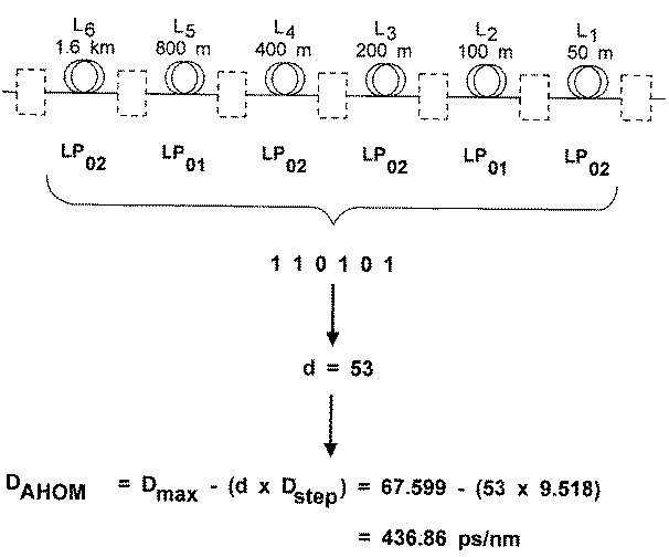
切り換え状態#53についてこれらの関係を示すフローチャートが図6に示されており、それは装置の分散値DAHOM=−436.855ps/nmに相当する。反対に、所望の分散Dtargetが与えられると、逆の計算が2進数を生じ、それが各MCの切り換え状態を独特に規定する。このフローチャートはDtarget=−200ps/nmに関して図7に示されている。この目標に関して得られる構成はDAHOM=−198.9ps/nmを生じる。
A flow chart showing these relationships for switching
図8は、様々なMC切り換え状態0、10、20、30、40、50、60および63それぞれに関するこのAHOMの広帯域分散調整特性を示している。この装置の帯域幅がMCの帯域幅によってのみ制限されることに留意すべきである。60nmを超える帯域幅を備えたLPG MC群を示してきたので、GDリップルのようないかなる付加的な障害も加えずにそのような装置が光通信システムのCまたはL帯域全体をカバーすることは明らかである。付け加えると、この装置の分散調整範囲はスプールのHOMファイバの長さを変えることによって、またはさらに多くの区画を追加することによって変えることが可能である。 FIG. 8 shows the wideband dispersion tuning characteristics of this AHOM for the various MC switching states 0, 10, 20, 30, 40, 50, 60 and 63, respectively. It should be noted that the bandwidth of this device is limited only by the MC bandwidth. Having shown LPG MCs with bandwidths in excess of 60 nm, it is not possible for such devices to cover the entire C or L band of an optical communication system without adding any additional obstacles such as GD ripple. it is obvious. In addition, the dispersion adjustment range of this device can be changed by changing the length of the HOM fiber in the spool or by adding more sections.
上記で示した範例は2進の長さ数列のHOMファイバの6つの区画(式1でN=6)および2つのモード(式1でM=2)を使用する。多数の別の選択肢となる装置構成が使用される可能性がある。例えば、いかなる所望の分散調整範囲、過程のサイズおよび分散値も達成するように2つよりも多くのモード(M>2)、異なる数の区画(N)、および異なるHOMファイバ長さの数列を装置が使用する可能性がある。場合によっては、HOMファイバの異なる区画が、異なる分散、分散勾配、および分散曲線特性を備えたHOMファイバを有して、その結果、装置を組み立てる追加的な自由度を生じることも可能である。これらすべては広帯域で調整可能な分散補償装置ばかりでなく、調整可能な分散勾配および/または分散曲線の補償装置を生じることも可能である。最も一般的な構成では、AHOMは波長との関係となる分散のいかなる所望の関数的変化も生じるように調整される可能性がある。 The example given above uses 6 sections of binary length sequence HOM fiber (N = 6 in Equation 1) and 2 modes (M = 2 in Equation 1). Numerous alternative device configurations may be used. For example, a sequence of more than two modes (M> 2), different numbers of partitions (N), and different HOM fiber lengths to achieve any desired dispersion tuning range, process size and dispersion value. The device may use it. In some cases, different sections of the HOM fiber can have HOM fibers with different dispersion, dispersion slope, and dispersion curve characteristics, resulting in additional freedom to assemble the device. All of this can result in not only a broadband adjustable dispersion compensator, but also an adjustable dispersion slope and / or dispersion curve compensator. In the most common configuration, the AHOM can be adjusted to produce any desired functional change in dispersion that is related to wavelength.
前に述べたように、この装置の重要な構成要素は切り換え可能なMCである。筆者の係属出願(前記参照)に記載および権利主張されているMCは特に適しているが、別の選択肢のMC装置が使用されることも可能である。これらは中でも、例えば、結合型導波路、位相遅延プレート、MEM装置を使用することがあり得る。これらのMC装置は切り換え動作の性能を有していなければならない。歪力、温度または電子−光学もしくは非線形光学変化によって変えることのできる屈折率を有する、装置構造内の光学材料層に含まれることで切り換えが実現される可能性もある。場合によっては、切り換え動作は歪力印加、そうでなければ装置の光学経路長を変えることによって達成されることも可能である。LPG群が音響−光学励起によって形成される場合、グレーティングの周期は、ファイバに印加される音響−光学変調の周波数を変えることによって変えることが可能である。 As previously mentioned, an important component of this device is a switchable MC. The MC described and claimed in my pending application (see above) is particularly suitable, although alternative MC devices can be used. Among these, for example, a coupled waveguide, a phase delay plate, and a MEM device may be used. These MC devices must have switching performance. Switching may also be realized by inclusion in an optical material layer in the device structure having a refractive index that can be changed by strain, temperature, or electro-optic or nonlinear optical changes. In some cases, the switching action can be accomplished by applying a strain force, otherwise changing the optical path length of the device. If the LPG group is formed by acousto-optic excitation, the period of the grating can be changed by changing the frequency of the acousto-optic modulation applied to the fiber.
適切な別の選択肢が図9のシステム規模に示されている。ここでは目的は電子−光学材料、例えばニオブ酸リチウムでMC素子を形成することであり、そこでは便利な電気的切り換え手段を備えた導波路の大きなアレーが集積化可能である。図9は電子−光学、非線形光学、または音響−光学材料の基板91を示している。基板91は、図4に示した装置のMC装置MC1〜MC7の各々について1つとして、7つの導波路92a〜92gを含む。光ファイバ経路は入力部93、出力部94、および光ファイバ・スプール95a〜95fを含む。スプール95a〜95fは図4の装置のスプールL1〜L6に相当する。切り換え素子は97で示される。それらは導波路内のカップラもしくはグレーティング(図示せず)に被せられた金属フィルム電極を有する。金属フィルム電極は図示したランナーによって適切な電圧源に相互接続される。
Another suitable option is shown in the system scale of FIG. The object here is to form the MC element with an electro-optical material, for example lithium niobate, where a large array of waveguides with convenient electrical switching means can be integrated. FIG. 9 shows a substrate 91 of electro-optic, nonlinear optics or acousto-optic material. Substrate 91, as one for each of the
モード変換器との関連で説明した長周期グレーティングは様々な技術によって形成されることが可能である。一般的な手法はドープしたファイバにUV光を使用してグレーティングを書き込むものである。そのようなグレーティングはまた、熱、圧力、またはUV光以外の光に起因する周期指数の変化を導入することによって実現されることも可能である。しかしながら、他の方法もやはり使用される可能性がある。例えば、マイクロベンドを導入したLPGが適切である。これらは音響−光学グレーティング、アーク・スプライサで導入した周期的マイクロベンドで、または必要なグレーティング周期性を有する波型のブロックの間にファイバを押圧することによって実現される可能性もある。 The long period grating described in connection with the mode converter can be formed by various techniques. A common approach is to write a grating using UV light in a doped fiber. Such a grating can also be realized by introducing changes in the periodic index due to heat, pressure, or light other than UV light. However, other methods may still be used. For example, LPG with a microbend introduced is appropriate. These may be realized with acousto-optic gratings, periodic microbends introduced with arc splicers, or by pressing the fiber between corrugated blocks with the required grating periodicity.
上記で説明したAHOM装置は多くの度合いの設計自由度を有する。これらのうちのいくつかは異なる長さの光ファイバ・スプールの使用に帰することができる。これは2つ(またはそれ以上)の伝搬モード用に選択した相対的経路長に応じて全体的分散値が変えられることを可能にする。光ファイバの長さは、たとえそれらが同じ長さであっても所定のモードに関して異なる分散値を有するように選択もしくは設計されることが可能である。さらに、2つのモードは同じファイバ内で異なる分散値で伝搬するので、ファイバの長さが等しいか、またはほぼ等しい図4のような装置は、それでもなお本発明の利点を提供することが可能である。 The AHOM device described above has many degrees of design freedom. Some of these can be attributed to the use of different length fiber optic spools. This allows the overall dispersion value to be varied depending on the relative path length chosen for the two (or more) propagation modes. The lengths of the optical fibers can be selected or designed to have different dispersion values for a given mode even if they are the same length. Furthermore, since the two modes propagate in the same fiber with different dispersion values, a device such as FIG. 4 where the fiber lengths are equal or nearly equal can still provide the advantages of the present invention. is there.
2つよりも多いコア導波モードを使用するシステムに本発明の原理が適用され得ることは明らかなはずである。前述した装置で、装置の各ステージ、すなわち、例えば図4の各長さL1〜L6について同じ2つのモードが想定されている。場合によっては、異なるファイバ区画が使用され、そこでは2つのモードが異なることもあり得る。例えば、装置の一方のステージ用に選択されるモードがLP01とLP02である場合、装置の他方のステージ用に選択されるモードがLP11とLP02であることも可能である。 It should be apparent that the principles of the present invention can be applied to systems that use more than two core guided modes. In the apparatus described above, the same two modes are assumed for each stage of the apparatus, that is, for example, for each of the lengths L 1 to L 6 in FIG. In some cases, different fiber sections are used, where the two modes may be different. For example, if the modes selected for one stage of the apparatus are LP 01 and LP 02 , the modes selected for the other stage of the apparatus may be LP 11 and LP 02 .
やはり本発明の範囲内にあるものは、多重HOM光ファイバ区画を備えたAHOM装置であって、そこでは異なる区画は異なるファイバ設計と特性を有する。このケースでは、異なるHOMファイバ内で同じ次数のモードに起因する分散が異なるであろう。これは、調整可能な分散、分散勾配、分散曲線、または波長の関数となる分散のいずれか任意の高次派生物であるいかなる光学特性も供給する装置を生じる。 Also within the scope of the present invention is an AHOM device with multiple HOM fiber optic sections, where the different sections have different fiber designs and characteristics. In this case, the dispersion due to the same order mode in different HOM fibers will be different. This results in a device that supplies any optical property that is any higher order derivative of tunable dispersion, dispersion slope, dispersion curve, or dispersion as a function of wavelength.
本発明によるAHOM装置は光通信システムに数多くの用途を有する。図10はAHOM装置によって可能になる光通信システムの1つの好ましい実施形態を示す。図10aは光ファイバ伝送ラインの概略を示しており、そこでは光信号は予め決められた長さの伝送ファイバ101を通じて伝送され、光学増幅モジュール102がその後に続く。光学増幅モジュール102はその入力部と出力部それぞれに利得ブロック103を有する。利得ブロック103は、本発明によるAHOM装置104、および既存の通信システムで一般に使用される静的分散補償装置(スタティックDC)105によって互いに接続される。図10bは類似した光通信システムを示しており、そこでは分散補償のすべてはAHOM装置だけによって供給され、スタティックDCを必要とせずに済む。予め決められた長さの伝送ファイバを通って伝送された後では、信号は減衰される。それはまた、時間または伝送ファイバの特異的分散特性で変化する可能性のある分散の有意の量を蓄積する。利得ブロックは信号パワーの損失を補償するのに必要な増幅を提供する。AHOM装置は信号によって蓄積された分散を補償するために調整可能な分散を提供する。2つの図式、図10aと10bは、AHOM装置がスタティックDCによって提供される分散補償の大部分でもって調整可能な分散補正を提供するか、あるいは信号にとって必要な分散補償のすべてを提供するかのいずれかである可能性があることを例示している。
The AHOM device according to the present invention has many uses in optical communication systems. FIG. 10 shows one preferred embodiment of an optical communication system enabled by an AHOM device. FIG. 10a shows a schematic of an optical fiber transmission line, where the optical signal is transmitted through a predetermined length of
図11はAHOM装置によって可能となる光通信システムの別の好ましい実施形態を示している。図11aは、光学増幅モジュール111、その後に続いて、入来光学信号を電気信号へと変換する光学検出機構115を有する受信装置の概略を示す。光学増幅モジュール111はその入力部と出力部それぞれに利得ブロック112を有する。利得ブロック112は、本発明によるAHOM装置113、および既存の通信システムで一般に使用されるスタティックDC114によって互いに接続される。図11bは類似した光通信システムを示しており、そこでは分散補償のすべてがAHOM装置だけによって供給され、スタティックDCを必要とせずに済む。2つの図式、図11aと11bは、AHOM装置がスタティックDCによって提供される分散補償の大部分でもって調整可能な分散補正を提供するか、あるいは光学検出装置に入る前の信号にとって必要な分散補償のすべてを提供するかのいずれかである可能性があることを例示している。光学検出機構115のエレクトロニクス部分は、AHOM装置の分散を変えることによってフィードバック・メカニズムが受信装置の性能を最適化するように、光学増幅モジュール111内のAHOM装置113の電気的制御部に接続されることが可能である。
FIG. 11 shows another preferred embodiment of an optical communication system enabled by an AHOM device. FIG. 11a shows a schematic of a receiving device having an optical amplification module 111 followed by an
本発明の様々な追加的改造が当業者に生じるであろう。本原理および技術を進歩させてきたそれと同等のものに基本的に頼るもので、本明細書の特異的教示から逸脱するものはすべて、記述および権利主張した本発明の範囲内であると考えることが適切である。 Various additional modifications of the present invention will occur to those skilled in the art. Any reliance on the principles and equivalents that have been made to advance the technology, fundamentally deviating from the specific teachings herein, shall be considered within the scope of the invention as described and claimed. Is appropriate.
Claims (6)
b.少なくとも前記第1のモードと前記第2のモードとをサポートし、そして前記第1のモードの光信号に対して第1の分散値を、そして前記第2のモードの光信号に対して第2の分散値を有する、長さL1を有する第1の長さの光ファイバと、
c.前記光信号を第2のモードから前記第2のモードとは異なる第3のモードへ変換する第1のスイッチ状態と前記光信号を前記第2のモードから前記第3のモードへは変換しない第2のスイッチ状態とを有し、これにより光信号出力を生成する第2のモード変換器と、
d.前記第1のモード変換器を前記第1のスイッチ状態へ切り替えて第1の分散値で前記光信号出力を生成し、そして前記第1のモード変換器を前記第2のスイッチ状態へ切り替えて前記第2の分散値で前記光信号出力を生成するスイッチ素子とを含むことを特徴とする光学装置。 a. A first mode having a first switch state that converts an optical signal from a first mode to a second mode and a second switch state that does not convert the optical signal from a first mode to a second mode A converter,
b . Supports at least the first mode and the second mode, and the first dispersion value to the optical signal of the first mode, and the optical signal of the second mode a second distribution value for a first length of optical fiber having a length L 1,
c. A first switch state for converting the optical signal from the second mode to a third mode different from the second mode, and a first switch state for converting the optical signal from the second mode to the third mode. A second mode converter having two switch states and thereby generating an optical signal output;
d. Switching the first mode converter to the first switch state to generate the optical signal output at a first dispersion value, and switching the first mode converter to the second switch state; An optical device including a switch element that generates the optical signal output with a second dispersion value .
e.少なくとも第3のモードと前記第3のモードとは異なるモードとをサポートし、そして前記第3のモードの光信号に対して第1の分散値を、そして前記第3のモードとは異なるモードの光信号に対して第2の分散値を有する、長さLe. Support at least a third mode and a mode different from the third mode, and a first dispersion value for the optical signal of the third mode, and a mode different from the third mode. A length L having a second dispersion value for the optical signal 22 を有する第2の長さの光ファイバと、A second length of optical fiber having:
f.前記光信号を前記第3のモードから前記第3のモードとは異なるモードへ変換する第1のスイッチ状態と前記光信号を前記第3のモードから前記第3のモードとは異なるモードへは変換しない第2のスイッチ状態とを有し、これにより光信号出力を生成する第3のモード変換器と、f. A first switch state for converting the optical signal from the third mode to a mode different from the third mode, and converting the optical signal from the third mode to a mode different from the third mode. A third mode converter having a second switch state that does not, thereby generating an optical signal output;
g.前記第2のモード変換器を前記第1のスイッチ状態へ切り替えて、前記第2の長さの光ファイバの前記第1の分散値で前記光信号出力を生成し、そして前記第2のモード変換器を前記第2のスイッチ状態へ切り替えて、前記第2の長さの光ファイバの前記第2の分散値で前記光信号出力を生成するスイッチ素子とを含むことを特徴とする光学装置。g. Switching the second mode converter to the first switch state to generate the optical signal output at the first dispersion value of the second length of optical fiber and the second mode conversion; An optical device comprising: a switch element for switching the device to the second switch state to generate the optical signal output at the second dispersion value of the second length of optical fiber.
b.少なくとも前記第1のモードと前記第2のモードとをサポートし、そして前記光信号が前記第1のモードであるときには第1の分散値を有し、そして前記光信号が前記第2のモードであるときには第2の分散値を有する、長さLb. Supports at least the first mode and the second mode, and has a first dispersion value when the optical signal is in the first mode, and the optical signal is in the second mode. A length L, sometimes having a second variance value 11 を有する第1の長さの光ファイバを介して前記光信号を伝送するステップと、Transmitting the optical signal through a first length optical fiber having:
c.前記光信号を第2のモードから前記第2のモードとは異なるモードへ変換する第1のスイッチ状態と前記光信号を第2のモードから前記第2のモードとは異なるモードへは変換しない第2のスイッチ状態とを有する第2のモード変換器を介して前記光信号を伝送するステップとを含み、前記第2のモード変換器が、前記第1のスイッチ状態の前記第1のモード変換器で切り替えられ、そして前記第2のスイッチ状態の前記第1のモード変換器で切り替えられることができ、これにより、光信号出力を生成するものであり、さらに、c. A first switch state for converting the optical signal from a second mode to a mode different from the second mode, and a first switch state for converting the optical signal from a second mode to a mode different from the second mode. Transmitting the optical signal via a second mode converter having two switch states, wherein the second mode converter is in the first switch state. And can be switched with the first mode converter in the second switch state, thereby generating an optical signal output, and
d.前記第1のモード変換器を前記第1のスイッチ状態に切り替えて、前記第1の分散値で光信号出力を生成するステップと、d. Switching the first mode converter to the first switch state to generate an optical signal output at the first dispersion value;
e.前記第2のモード変換器を前記第2のスイッチ状態に切り替えて、前記第2の分散値で光信号出力を生成するステップとを含むことを特徴とする方法。e. Switching the second mode converter to the second switch state to generate an optical signal output at the second dispersion value.
Applications Claiming Priority (1)
| Application Number | Priority Date | Filing Date | Title |
|---|---|---|---|
| US10/234,287 US6937788B2 (en) | 2002-09-04 | 2002-09-04 | Adjustable dispersion compensator with few mode fibers and switchable mode converters |
Publications (3)
| Publication Number | Publication Date |
|---|---|
| JP2004104782A JP2004104782A (en) | 2004-04-02 |
| JP2004104782A5 JP2004104782A5 (en) | 2005-05-26 |
| JP3875673B2 true JP3875673B2 (en) | 2007-01-31 |
Family
ID=31715286
Family Applications (1)
| Application Number | Title | Priority Date | Filing Date |
|---|---|---|---|
| JP2003312229A Expired - Fee Related JP3875673B2 (en) | 2002-09-04 | 2003-09-04 | Adjustable dispersion compensator with multimode fiber and switchable mode converter |
Country Status (9)
| Country | Link |
|---|---|
| US (1) | US6937788B2 (en) |
| EP (1) | EP1396742B1 (en) |
| JP (1) | JP3875673B2 (en) |
| KR (1) | KR100941983B1 (en) |
| CN (1) | CN1497279B (en) |
| AU (1) | AU2003244566B2 (en) |
| CA (1) | CA2437877C (en) |
| DE (1) | DE60314210T2 (en) |
| IL (1) | IL157502A (en) |
Families Citing this family (25)
| Publication number | Priority date | Publication date | Assignee | Title |
|---|---|---|---|---|
| US7519295B2 (en) * | 2003-10-30 | 2009-04-14 | Tyco Telecommunications (Us) Inc. | Apparatus and method for commissioning an optical transmission system |
| US7177510B2 (en) * | 2004-08-09 | 2007-02-13 | Fitel Usa Corp. | Polarization insensitive microbend fiber gratings and devices using the same |
| JP2006145757A (en) * | 2004-11-18 | 2006-06-08 | Fujitsu Ltd | Dispersion compensator |
| US20070206910A1 (en) * | 2006-03-04 | 2007-09-06 | Siddharth Ramachandran | Optical fibers and optical fiber devices with total dispersion greater than material dispersion |
| JP4826462B2 (en) * | 2006-12-20 | 2011-11-30 | 株式会社日立製作所 | Dispersion compensator, optical transmission system, and optical transmission method |
| EP2109788B1 (en) * | 2007-02-05 | 2018-10-31 | Furukawa Electric North America Inc. | Segmented gain-doping of an optical fiber |
| US8270786B2 (en) * | 2008-11-21 | 2012-09-18 | Ofs Fitel, Llc | Optical fiber mode couplers |
| US8054892B2 (en) * | 2009-02-12 | 2011-11-08 | Agere Systems Inc. | Compensating transmission line to reduce sensitivity of performance due to channel length variation |
| US8818195B2 (en) | 2010-08-20 | 2014-08-26 | Adva Optical Networking Se | Method of operating an optical transmission system and optical transmission system |
| US8958703B2 (en) | 2011-03-04 | 2015-02-17 | Alcatel Lucent | Multipath channel for optical subcarrier modulation |
| EP3110041B1 (en) | 2011-06-30 | 2018-08-29 | Xieon Networks S.à r.l. | Method of reducing the modal delay in a multimode transmission system |
| WO2013023193A1 (en) * | 2011-08-10 | 2013-02-14 | Ofs Fitel, Llc | Few moded fiber device employing mode conversion |
| CN103907302B (en) * | 2011-09-02 | 2017-11-17 | 阿尔卡特朗讯 | Method and apparatus for SDM system |
| EP2645609B1 (en) * | 2012-03-30 | 2014-10-29 | Alcatel Lucent | Method of optical data transmission using mode division multiplexing |
| JP5893994B2 (en) * | 2012-04-02 | 2016-03-23 | 日本電信電話株式会社 | Optical fiber transmission system and optical fiber transmission method |
| CN102914421B (en) * | 2012-10-19 | 2015-08-12 | 苏州光环科技有限公司 | A kind of method for measuring polarization interference in optical birefringence medium and equipment thereof |
| JP6023020B2 (en) * | 2013-07-26 | 2016-11-09 | 日本電信電話株式会社 | Optical amplifier |
| WO2016070420A1 (en) | 2014-11-07 | 2016-05-12 | 华为技术有限公司 | Mode converter, and multimode waveguide transmission apparatus and method |
| CN104792402B (en) * | 2015-04-16 | 2017-07-28 | 华中科技大学 | A kind of sound wave sense measuring device based on optical fiber sagnac interferometer |
| CN105891957B (en) * | 2016-06-15 | 2019-01-08 | 北京邮电大学 | A kind of single order OAM pattern generation system of all -fiber |
| US10969611B2 (en) * | 2017-07-14 | 2021-04-06 | The Government Of The United States Of America, As Represented By The Secretary Of The Navy | Devices for transmitting a modulated optical signal using a few-mode fiber |
| JP6989793B2 (en) * | 2017-08-01 | 2022-02-03 | 日本電信電話株式会社 | Optical transmission system |
| JP7061771B2 (en) * | 2018-04-18 | 2022-05-02 | 日本電信電話株式会社 | Mode switch |
| CN112346174B (en) * | 2019-08-09 | 2022-12-02 | 华为技术有限公司 | A polymer waveguide and terahertz signal transmission method |
| RU2762850C1 (en) * | 2021-04-15 | 2021-12-23 | Федеральное государственное бюджетное образовательное учреждение высшего образования "Поволжский государственный университет телекоммуникаций и информатики" | Method for compensation of dispersion of a single-mode fiber-optic communication line |
Family Cites Families (9)
| Publication number | Priority date | Publication date | Assignee | Title |
|---|---|---|---|---|
| US5999671A (en) * | 1997-10-27 | 1999-12-07 | Lucent Technologies Inc. | Tunable long-period optical grating device and optical systems employing same |
| JP3570193B2 (en) | 1998-01-14 | 2004-09-29 | Kddi株式会社 | Optical transmission system |
| US6134258A (en) * | 1998-03-25 | 2000-10-17 | The Board Of Trustees Of The Leland Stanford Junior University | Transverse-pumped sLAB laser/amplifier |
| KR100274075B1 (en) * | 1998-05-09 | 2001-01-15 | 서원석 | Optical fiber grating and optical element using the same |
| US6151431A (en) * | 1998-11-24 | 2000-11-21 | Lucent Technologies Inc. | Compact non-blocking non-dilated optical switch using mode conversion |
| US6418256B1 (en) * | 1999-02-23 | 2002-07-09 | Lasercomm, Inc. | High order spatial mode optical fiber |
| DE19950132A1 (en) * | 1999-10-18 | 2001-04-19 | Siemens Ag | Chromatic dispersion compensation device for optical fibre system |
| US6417948B1 (en) * | 1999-12-24 | 2002-07-09 | Corning Incorporated | Variable delay device for an optical component such as a polarization mode dispersion compensator |
| WO2002054631A2 (en) * | 2000-12-30 | 2002-07-11 | University Of Rochester | Device and method for compensating for chromatic dispersion |
-
2002
- 2002-09-04 US US10/234,287 patent/US6937788B2/en not_active Expired - Lifetime
-
2003
- 2003-08-19 CA CA2437877A patent/CA2437877C/en not_active Expired - Fee Related
- 2003-08-20 IL IL157502A patent/IL157502A/en active IP Right Grant
- 2003-09-02 DE DE60314210T patent/DE60314210T2/en not_active Expired - Lifetime
- 2003-09-02 EP EP03019933A patent/EP1396742B1/en not_active Expired - Lifetime
- 2003-09-03 CN CN031581056A patent/CN1497279B/en not_active Expired - Fee Related
- 2003-09-04 AU AU2003244566A patent/AU2003244566B2/en not_active Ceased
- 2003-09-04 JP JP2003312229A patent/JP3875673B2/en not_active Expired - Fee Related
- 2003-09-04 KR KR1020030061674A patent/KR100941983B1/en not_active Expired - Fee Related
Also Published As
| Publication number | Publication date |
|---|---|
| JP2004104782A (en) | 2004-04-02 |
| US6937788B2 (en) | 2005-08-30 |
| DE60314210D1 (en) | 2007-07-19 |
| IL157502A (en) | 2008-06-05 |
| AU2003244566A1 (en) | 2004-03-25 |
| US20040047551A1 (en) | 2004-03-11 |
| CN1497279B (en) | 2010-05-26 |
| AU2003244566B2 (en) | 2008-11-13 |
| KR100941983B1 (en) | 2010-02-16 |
| EP1396742B1 (en) | 2007-06-06 |
| IL157502A0 (en) | 2004-03-28 |
| EP1396742A2 (en) | 2004-03-10 |
| CA2437877C (en) | 2011-10-25 |
| CN1497279A (en) | 2004-05-19 |
| KR20040021562A (en) | 2004-03-10 |
| EP1396742A3 (en) | 2004-06-02 |
| DE60314210T2 (en) | 2008-02-14 |
| CA2437877A1 (en) | 2004-03-04 |
Similar Documents
| Publication | Publication Date | Title |
|---|---|---|
| JP3875673B2 (en) | Adjustable dispersion compensator with multimode fiber and switchable mode converter | |
| US5943151A (en) | Mehtod of selectively compensating for the chromatic dispersion of optical signals | |
| US7013063B2 (en) | System for higher-order dispersion compensation including phase modulation | |
| US7593608B2 (en) | Optical communications system | |
| WO2002025845A2 (en) | Tunable optical dispersion by using two fiber bragg gratings with nonlinear group delays | |
| US7263257B2 (en) | Gires-Tournois etalons and dispersion compensation | |
| US6907199B2 (en) | Method for polarization mode dispersion compensation | |
| JP3728401B2 (en) | Fiber transmission element for producing chromatic dispersion | |
| GB2362527A (en) | A wavelength independant chromatic dispersion compensator | |
| Madsen et al. | An all-pass filter dispersion compensator using planar waveguide ring resonators | |
| US6768822B1 (en) | Chromatic dispersion compensation | |
| US20030031404A1 (en) | Optical transmission systems including optical components and optical filters and methods of use therein | |
| Ramachandran et al. | Tunable dispersion compensators utilizing higher order mode fibers | |
| US20030123776A1 (en) | System for polarization mode dispersion compensation | |
| Eggleton | Dynamic dispersion compensation devices for high speed transmission systems | |
| US7016567B2 (en) | System for higher-order dispersion compensation including a delay line | |
| Petruzzi et al. | Dispersion compensation using only fiber Bragg gratings | |
| Song et al. | Tunable dispersion slope compensation for 40-Gb/s WDM systems using broadband nonchannelized third-order chirped fiber Bragg gratings | |
| Takiguchi et al. | Integrated-optic dispersion slope equalizer for N× several tens of Gb/s WDM transmission | |
| EP1461881A2 (en) | Method for higher-order dispersion compensation | |
| Madsen et al. | Integrated optical allpass filters for dispersion compensation | |
| WO2002099483A1 (en) | Chromatic dispersion and dispersion slope control | |
| EP1461880A2 (en) | System for higher-order dispersion compensation including a delay line | |
| Takahashi et al. | Expansion of passband of tunable chromatic dispersion compensator based on ring resonators using negative group delay peak | |
| Otto et al. | Fiber optical structure for tunable dispersion compensation using cascaded long-period gratings |
Legal Events
| Date | Code | Title | Description |
|---|---|---|---|
| A521 | Request for written amendment filed |
Free format text: JAPANESE INTERMEDIATE CODE: A523 Effective date: 20040116 |
|
| A621 | Written request for application examination |
Free format text: JAPANESE INTERMEDIATE CODE: A621 Effective date: 20040116 |
|
| A131 | Notification of reasons for refusal |
Free format text: JAPANESE INTERMEDIATE CODE: A131 Effective date: 20060313 |
|
| A601 | Written request for extension of time |
Free format text: JAPANESE INTERMEDIATE CODE: A601 Effective date: 20060613 |
|
| A602 | Written permission of extension of time |
Free format text: JAPANESE INTERMEDIATE CODE: A602 Effective date: 20060616 |
|
| A521 | Request for written amendment filed |
Free format text: JAPANESE INTERMEDIATE CODE: A523 Effective date: 20060913 |
|
| TRDD | Decision of grant or rejection written | ||
| A01 | Written decision to grant a patent or to grant a registration (utility model) |
Free format text: JAPANESE INTERMEDIATE CODE: A01 Effective date: 20061002 |
|
| A61 | First payment of annual fees (during grant procedure) |
Free format text: JAPANESE INTERMEDIATE CODE: A61 Effective date: 20061026 |
|
| R150 | Certificate of patent or registration of utility model |
Ref document number: 3875673 Country of ref document: JP Free format text: JAPANESE INTERMEDIATE CODE: R150 Free format text: JAPANESE INTERMEDIATE CODE: R150 |
|
| FPAY | Renewal fee payment (event date is renewal date of database) |
Free format text: PAYMENT UNTIL: 20101102 Year of fee payment: 4 |
|
| R250 | Receipt of annual fees |
Free format text: JAPANESE INTERMEDIATE CODE: R250 |
|
| FPAY | Renewal fee payment (event date is renewal date of database) |
Free format text: PAYMENT UNTIL: 20111102 Year of fee payment: 5 |
|
| R250 | Receipt of annual fees |
Free format text: JAPANESE INTERMEDIATE CODE: R250 |
|
| FPAY | Renewal fee payment (event date is renewal date of database) |
Free format text: PAYMENT UNTIL: 20121102 Year of fee payment: 6 |
|
| R250 | Receipt of annual fees |
Free format text: JAPANESE INTERMEDIATE CODE: R250 |
|
| FPAY | Renewal fee payment (event date is renewal date of database) |
Free format text: PAYMENT UNTIL: 20131102 Year of fee payment: 7 |
|
| R250 | Receipt of annual fees |
Free format text: JAPANESE INTERMEDIATE CODE: R250 |
|
| R250 | Receipt of annual fees |
Free format text: JAPANESE INTERMEDIATE CODE: R250 |
|
| R250 | Receipt of annual fees |
Free format text: JAPANESE INTERMEDIATE CODE: R250 |
|
| R250 | Receipt of annual fees |
Free format text: JAPANESE INTERMEDIATE CODE: R250 |
|
| R250 | Receipt of annual fees |
Free format text: JAPANESE INTERMEDIATE CODE: R250 |
|
| R250 | Receipt of annual fees |
Free format text: JAPANESE INTERMEDIATE CODE: R250 |
|
| R250 | Receipt of annual fees |
Free format text: JAPANESE INTERMEDIATE CODE: R250 |
|
| LAPS | Cancellation because of no payment of annual fees |