JP3872370B2 - Voltage fluctuation compensation device - Google Patents
Voltage fluctuation compensation device Download PDFInfo
- Publication number
- JP3872370B2 JP3872370B2 JP2002093650A JP2002093650A JP3872370B2 JP 3872370 B2 JP3872370 B2 JP 3872370B2 JP 2002093650 A JP2002093650 A JP 2002093650A JP 2002093650 A JP2002093650 A JP 2002093650A JP 3872370 B2 JP3872370 B2 JP 3872370B2
- Authority
- JP
- Japan
- Prior art keywords
- voltage
- compensation
- value
- output
- energy storage
- Prior art date
- Legal status (The legal status is an assumption and is not a legal conclusion. Google has not performed a legal analysis and makes no representation as to the accuracy of the status listed.)
- Expired - Fee Related
Links
Images


Classifications
-
- Y—GENERAL TAGGING OF NEW TECHNOLOGICAL DEVELOPMENTS; GENERAL TAGGING OF CROSS-SECTIONAL TECHNOLOGIES SPANNING OVER SEVERAL SECTIONS OF THE IPC; TECHNICAL SUBJECTS COVERED BY FORMER USPC CROSS-REFERENCE ART COLLECTIONS [XRACs] AND DIGESTS
- Y02—TECHNOLOGIES OR APPLICATIONS FOR MITIGATION OR ADAPTATION AGAINST CLIMATE CHANGE
- Y02E—REDUCTION OF GREENHOUSE GAS [GHG] EMISSIONS, RELATED TO ENERGY GENERATION, TRANSMISSION OR DISTRIBUTION
- Y02E40/00—Technologies for an efficient electrical power generation, transmission or distribution
- Y02E40/30—Reactive power compensation
Description
【0001】
【発明の属する技術分野】
この発明は、負荷に供給される電力系統の電圧が瞬時的に低下した際に、それを検出して電圧低下を補償する電圧変動補償装置に関するものである。
【0002】
【従来の技術】
雷などにより電力系統の電圧が瞬時的に低下し、工場などの精密機器などが誤作動や一時停止することにより、生産ラインで多大な被害を被ることがある。このような被害を防ぐために、電力系統の瞬時的電圧低下などの電圧変動を監視して、電圧低下を補償する電圧変動補償装置が用いられている。
従来の電圧変動補償装置の概略構成図を図18に示す。図に示すように、送電線1からの電力は、変圧器2により降圧されて、電圧変動補償装置を介して需要家3(負荷)に接続され、電力が供給される。電圧変動補償装置は、直流電源4、インバータ5、平滑フィルタ6および大容量トランス7で構成される。
このような従来の電圧変動補償装置における、系統電圧の瞬時低下時(以下、瞬低時と称す)の電圧補償動作について以下に示す。
図19は、系統電圧の瞬低時の、系統電圧、電圧変動補償回路出力、および需要家3に供給される電圧をそれぞれ示したものである。図に示すように、系統電圧に瞬時的に電圧低下が発生すると、電圧変動を監視している検出部(図示せず)にて電圧低下を検出し、それに基づく給電制御により、電圧変動補償装置では、直流電源4とインバータ5とで交流電圧を発生させて、平滑フィルタ6と大容量のトランス7を介して電力系統に直列に接続することにより、電力系統の電圧低下を補償する。これにより、需要家3には、電圧低下した系統電圧に電圧変動補償装置からの出力電圧が加算されてほぼ正常な電圧で電力が供給される。
【0003】
【発明が解決しようとする課題】
従来の電圧変動補償装置は、以上のように構成されているため、系統電圧が正常の場合にも、トランス7を介して負荷電流相当分がインバータ5に流れ、これにより、トランス7とインバータ5との損失が通常時にも発生し、大型の冷却装置が必要であった。
また、系統電圧の瞬低時には、平滑フィルタ6およびトランス7を介して電力系統に電圧供給するため、平滑フィルタ6やトランス7の容量が大きくなり、装置が大型化するという問題点があった。
【0004】
この発明は、上記のような問題点を解消するために成されたものであって、系統電圧の瞬低時における高精度な電圧補償が可能で、装置全体が安価で小型に構成できる電圧変動補償装置を得ることを目的とする。
【0005】
【課題を解決するための手段】
この発明に係る電圧変動補償装置は、
接続される電力線の電圧変動を補償する電圧変動補償装置であって、
それぞれ異なる大きさのエネルギが蓄積される複数のエネルギ蓄積手段を有し、それぞれ前記蓄積されたエネルギを電圧として出力する複数の電圧補償回路と、
前記複数のエネルギ蓄積手段のそれぞれの検出電圧値を出力する電圧検出器と、
前記複数の電圧補償回路を制御して、前記電圧変動を補償する所定値の補償電圧を出力させる制御回路と
を備え、
前記複数の電圧補償回路は直列に接続され、
前記制御回路は、前記複数のエネルギ蓄積手段のそれぞれの検出電圧値と、前記電圧変動から得られる目標電圧値とに基づいて、前記複数の電圧補償回路の出力を組み合わせて前記所定値の補償電圧を出力させること
としたものである。
【0006】
また、この発明に係る電圧変動補償装置は、
接続される電力線の電圧変動を補償する電圧変動補償装置であって、
それぞれ異なる大きさのエネルギが蓄積される複数のエネルギ蓄積手段を有し、それぞれ前記蓄積されたエネルギを電圧として出力する複数の電圧補償回路と、
前記複数のエネルギ蓄積手段のそれぞれの予測電圧値を出力する予測電圧回路と、
前記複数の電圧補償回路を制御して、前記電圧変動を補償する所定値の補償電圧を出力させる制御回路と
を備え、
前記複数の電圧補償回路は直列に接続され、
前記制御回路は、前記複数のエネルギ蓄積手段のそれぞれの予測電圧値と、前記電圧変動から得られる目標電圧値とに基づいて、前記複数の電圧補償回路の出力を組み合わせて前記所定値の補償電圧を出力させること
としたものである。
【0018】
【発明の実施の形態】
実施の形態1.
以下、この発明の実施の形態1について詳細に説明する。
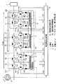
図1は、この発明の実施の形態1による電圧変動補償装置の構成図である。
送電線1からの電力は、変圧器2により降圧されて、電圧変動補償装置100を介して需要家3(負荷)に接続され、電力が供給される。
電圧変動補償装置100においては、図に示すように、電力系統に、電圧の極性に応じて選択される2つの電圧補償回路P、Nからなる補償ユニット110が複数個直列に接続される。この直列接続された複数個(この場合6個)の電圧補償回路N1、P1、N2、P2、N3、P3で構成される全補償回路120は、その出力端に全補償回路120と並列に、高速機械式の定常短絡スイッチ8を備える。
各電圧補償回路P1〜P3、N1〜N3には、出力端に並列に備えられた瞬低切替スイッチ9、瞬低補償スイッチ10、エネルギ蓄積手段としての充電コンデンサ11、および充電コンデンサ11を充電するための充電ダイオード12と充電用トランス200の2次巻線14とが備えられ、充電コンデンサ11の充電電圧はこの充電コンデンサ11に直列に接続された瞬低補償スイッチ10によって電力系統に接続される。また、瞬低切替スイッチ9および瞬低補償スイッチ10は、ダイオードが逆並列に接続された半導体スイッチング素子、例えばIGBTにて構成されている。なお、半導体スイッチング素子はIGBT以外の自己消弧型素子でも構わない。
【0019】
充電コンデンサ11は充電ダイオード12と充電用トランス200の2次巻線14によって電圧が充電され、充電用トランス1次巻線13は、電力系統と接続される。なお、15は充電用トランス200のコアである。
1つの補償ユニット110内の2つの電圧補償回路P、Nは、それぞれ正・負の電圧発生をつかさどる。つまり、2つの充電ダイオード12p、12nの作用により、充電コンデンサ11pと充電コンデンサ11nとには共通の2次巻線14を用いてそれぞれ逆極性の電圧が同じ大きさで充電されている。
各補償ユニット110内の充電コンデンサ11((11p1,11n1)(11p2,11n2)(11p3,11n3))に充電される電圧の比は概ね2のべき乗比に設定されている。つまり、以下の関係を満足させる。
Vn3=2×Vn2=2×2×Vn1 (pも同様)
【0020】
定常短絡スイッチ8、瞬低切替スイッチ9、瞬低補償スイッチ10は、検出制御部としての電圧瞬低制御回路16に接続される。また、系統電圧も電圧瞬低制御回路16に入力される。この電圧瞬低制御回路16の構成および動作について、以下に説明する。
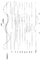
図2は、電圧瞬低制御回路16の詳細を示す回路図である。また、図3は、図1で示した電圧変動補償装置100による電圧補償の動作と電圧瞬低制御回路16の制御動作との関係を示す波形図である。
図2に示すように、系統電圧は電圧瞬低制御回路16に入力され、目標電圧25と比較される。このとき目標電圧25は、正常時の系統電圧とする。両者の差を誤差増幅器26にて増幅し、さらに絶対値変換を施した後、A/Dコンバータ27にて3ビットのデジタル信号(D1〜D3)に変換する。系統電圧と目標電圧25との差が、充電コンデンサ11p1の充電電圧Vp1と等しくなったとき、A/Dコンバータ27からの出力信号における最下位ビットのみが1、即ち゛001゛となるよう、誤差増幅器26のゲインは予め調整しておく。
【0021】
D1〜D3の信号のいずれかが1となると、NOR回路28を通して、信号Z(=0)により定常短絡スイッチ8をオフする。
一方、電圧瞬低制御回路16に入力された系統電圧は、極性判定回路29にも入力され、極性が判定される。次いで、系統電圧の極性が正・負の場合に応じて、デジタル信号D1〜D3にてアクテイブとなる信号YpもしくはYn、XpもしくはXnをAND回路30および反転器31を経て選択する。Xp、Xnは瞬低補償スイッチ10の駆動信号で、Yp、Ynは瞬低切替スイッチ9の駆動信号であり、瞬低切替スイッチ9と瞬低補償スイッチ10とは常に逆極性にて動作するよう反転器31にて構成されている。
系統電圧が正常時、即ちデジタル信号D1〜D3が全て0の時は、定常短絡スイッチ8はオン(信号Zは1)、瞬低切替スイッチ9はオン(信号Yは1)、瞬低補償スイッチ10はオフ状態(信号Xは0)にあり、電流は定常短絡スイッチ8を流れる。このとき充電コンデンサ11は充電用トランス200によって一定の電圧に充電されている。充電用トランス200は、充電コンデンサ11を充電するのみの働きでよいから、小容量のもので済む。
【0022】
次に、瞬低時の補償動作を図3に基づいて説明する。
時刻t0において、系統電圧に瞬時的に電圧低下が発生したとする。時刻t0以降に誤差増幅回路26の出力には誤差電圧が発生する。それに応じて、A/Dコンバータ27の出力には、誤差電圧に応じてデジタル信号D1〜D3が発生する。それと同時に、信号Zが0となり、定常短絡スイッチ8はオフする。
時刻t0〜t1は系統電圧の極性が正であるから、デジタル信号D1〜D3は、それぞれp側素子に伝達される。最下位ビットの信号D1が1のとき、電圧補償回路P1において、Xp1が1、Yp1が0となり、瞬低補償スイッチ10p1がオン、瞬低切替スイッチ9p1がオフして、充電コンデンサ11p1の電圧Vp1が瞬低補償スイッチ10p1により出力される。信号D2が1のときは、電圧補償回路P2において、Xp2が1、Yp2が0となり、瞬低補償スイッチ10p2がオン、瞬低切替スイッチ9p2がオフして、充電コンデンサ11p2の電圧Vp2が瞬低補償スイッチ10p2により出力される。同様に、最上位ビットの信号D3が1のとき、電圧補償回路P3において充電コンデンサ11p3の電圧Vp3が出力される。なお、各デジタル信号D1〜D3のうち0となる信号については、例えば最下位ビットの信号D1が0のとき、電圧補償回路P1において、Xp1が0、Yp1が1であるので、瞬低切替スイッチ9p1によって出力端が短絡されて電圧補償回路P1からの出力はほぼゼロとなる。これらの出力は、系統にて組み合わされ、゛000゛〜゛111゛の8階調の電圧出力を発生することができ、最大の補償電圧は、7×Vp1となる。
時刻t1〜t2までは、系統電圧の極性が負であるから、デジタル信号D1〜D3は、それぞれn側素子に伝達されて、電圧補償回路N1〜N3において同様に補償電圧を出力し、最大の補償電圧は、7×Vn1となる。
【0023】
ところで、上記説明では、充電コンデンサ11の電圧変化は考慮せず、理想的な状態の動作説明であるが、実際にはコンデンサ容量は有限であるため、充電コンデンサ11にはサグ(電圧の低下)が発生する。例えば充電コンデンサ11p3の充電電圧Vp3にサグが発生した場合、図2で示した電圧瞬低制御回路16を用いて上述したような2進の信号(D1〜D3)を形成し、電圧補償動作させると、図4に示すように、充電電圧Vp3のサグによって、発生する補償電圧にひずみが生じてしまう。
このため、図2で示したA/Dコンバータ27で2進の信号を出力するA/D変換を、上記充電コンデンサ11のサグを考慮して行うのが良く、これについて以下に示す。
【0024】
図5は、充電コンデンサ11の電圧低下を考慮したA/D変換を行うA/Dコンバータ27の詳細を示す構成図である。図において、50(50-1、50-2、50-3)はコンパレータ、51-1、51-2は演算プロセッサなどを用いた演算回路である。また、各電圧補償回路P1〜P3、N1〜N3内の充電コンデンサ11は電圧検出器を備えて電圧をモニタしており、電圧検出値V3、V2、V1をA/Dコンバータ27に入力する。なおこの場合、V3、V2、V1は、それぞれp側素子の充電コンデンサ11p3、11p2、11p3の電圧検出値とする(図1参照)。
図5に示すように、まず、誤差増幅器26の出力V3inとV3の電圧をコンパレータ50-3にて比較し、V3in≧V3のとき1、V3in<V3のとき0としてD3を形成する。次に、演算回路51-2において、D3が1なら、V2in=V3in−V3とし、D3が0のときはV2in=V3inとする。ここでV2inは、D3の信号状態において補償電圧を出力した場合の、補償できていない電圧を表す。次に、V2inとV2とをコンパレータ50-2にて比較しD2を出力する。次に先と同様に演算回路51-1にて、V1inを演算する。V1inは、D3とD2の信号状態において補償電圧を出力した場合の、補償が不足する電圧を表す。最後にV1inとV1とをコンパレータ50-1にて比較し、D1を決定する。
【0025】
このように、図5に示すようなA/Dコンバータ27を用いて、電力系統の電圧低下量を増幅した誤差増幅器26の出力を2進数の信号(D1〜D3)にA/D変換する際、各充電コンデンサ11の電圧を随時検出した電圧検出値V3、V2、V1と照合して2進数の信号の各ビット信号を決定する。このため、充電コンデンサ11の電圧状態に応じて、電圧補償回路P1〜P3、N1〜N3を選択して動作させる信号を決定するから、精度のよい補償が実現できる。それにより、充電コンデンサ11にサグが発生した場合でも、補償電圧にひずみが発生しないため、充電コンデンサ11の静電容量値を低減できる。
【0026】
また上記実施の形態1では、直列接続された複数個の電圧補償回路N1、P1、N2、P2、N3、P3で構成される全補償回路120が直接電力系統に直列に接続されているため、従来のような大型のトランスが不要である。また、全補償回路120と並列に、高速機械式の定常短絡スイッチ8を備えて、系統電圧510が正常時には定常短絡スイッチ8が導通して電流をバイパスするため、正常時の装置ロスはほとんどゼロとなり、冷却装置が小容量でよく、装置全体が安価で小型化できる。
また、系統電圧が瞬時低下したときには、それぞれ異なる電圧が充電された充電コンデンサ11を有する複数個の電圧補償回路N1、P1、N2、P2、N3、P3をディジタル階調制御により組み合わせを選択して、出力電圧の総和で電圧補償するため、きめ細かい電圧補償が可能になり、出力フィルタが不要または小型でよい。また、一般に用いられるPWM制御の場合などで出力フィルタの帯域分に相当する応答遅れが発生するのに比して、制御方式がデジタル階調制御であるため、リアルタイムで電圧を補償でき、さらに精度良く電圧補償が可能である。
【0027】
また、各電圧補償回路P1〜P3、N1〜N3の充電コンデンサ11に充電される電圧は、Vn3=2×Vn2=2×2×Vn1(pも同様)としたため、補償電圧を等間隔で高精度に階調制御できる。
さらに充電コンデンサ11は、電力系統に接続された充電用トランス200を介して、系統電圧の正常時にゆっくり充電できるため、充電用トランス200は小容量で十分であり、充電回路は小型・安価となる。また、自動的に充電が行われるため装置が簡素化される。
【0028】
なお、上記実施の形態では、A/Dコンバータ27で用いたV3、V2、V1は、それぞれp側素子の充電コンデンサ11p3、11p2、11p1の電圧検出値としたが、瞬時低下した電圧の大きさが、系統電圧の極性によらずほぼ一定の場合、n側素子の各充電コンデンサ11nの電圧もp側素子とほぼ同様に電圧状態が推移するため、p側、n側のいずれの電圧を検出してその絶対値を用いてもよい。
また、p側用とn側用の2個のA/Dコンバータ27を備えて、それぞれ対応する充電コンデンサ11の電圧検出値を入力して2進数の信号(D1〜D3)を発生させてもよく、その場合は、極性判定回路29(図2参照)の出力に合わせて、2個のA/Dコンバータ27のいずれかの出力信号を選択して用いる。これにより、さらに精度の高い補償が実現できる。
さらにまた、電圧検出器をp側用とn側用との双方に備え、極性判定回路29の出力に合わせて、p側、n側のいずれかの電圧検出器を選択して、その電圧検出値を用いてもよい。
【0029】
また、上記実施の形態1では、全補償回路120の出力端に全補償回路120と並列に、定常短絡スイッチ8を1個備えたが、図6に示すように、各電圧補償回路P1〜P3、N1〜N3の出力端毎に並列に備えても良い。また、一対の電圧補償回路P、Nから成る各補償ユニット110の出力端毎に、定常短絡スイッチ8を備えても良い。このように定常短絡スイッチ8が複数個備えられても、制御方式は1個の場合と同様であり、通常時には全ての定常短絡スイッチ8を閉じて全ての電圧補償回路P1〜P3、N1〜N3をバイパスし、電力系統の電圧低下時には全ての定常短絡スイッチ8を開放して電圧補償回路P1〜P3、N1〜N3からの電圧出力により電力系統の電圧低下を補償する。
【0030】
さらにまた、上記実施の形態1では、一対の電圧補償回路P、Nで補償ユニット110を構成したが、図7に示すように、1つの電圧補償回路PNで正負の電圧を出力する各補償ユニット110を構成しても良い。
図7(a)に示す例では、電圧補償回路PN1は、ダイオードが逆並列に接続された4個の半導体スイッチング素子17a〜17dから成るフルブリッジインバータ、およびエネルギ蓄積手段としての充電コンデンサ18を備え、充電コンデンサ18の充電電圧Vpn1は、半導体スイッチング素子17a〜17dのオン/オフ制御により正負いずれかの極性で電力系統に接続される。また図7(b)に示す例では、電圧補償回路PN1は、ダイオードが逆並列に接続された2個の半導体スイッチング素子19p1、19n1から成るハーフブリッジインバータ、ダイオードが逆並列に接続された2個の半導体スイッチング素子20p1、20n1が逆方向に直列接続されて、電圧補償回路PN1の出力端に並列に接続される瞬低切替スイッチ、およびエネルギ蓄積手段としての充電コンデンサ21p1、21n1を備え、半導体スイッチング素子19、20のオン/オフ制御により正負いずれかの極性の補償電圧が出力される。
【0031】
実施の形態2.
次に、この発明の実施の形態2について説明する。
図8は、この発明の実施の形態2によるA/Dコンバータ27の詳細を示す構成図である。図に示すように、A/Dコンバータ27は各充電コンデンサ11の電圧を予測演算する予測演算回路52(52-1、52-2、52-3)を備えている。また、電力系統の系統電流をモニタしており、各予測演算回路52には、系統電流の電流値と、このA/Dコンバータ27からの出力である各デジタル信号(D1〜D3)内の対応する信号とが入力される。各予測演算回路52では、系統電流の電流値と各デジタル信号(D1〜D3)とによって、各充電コンデンサ11の電圧値を予測して演算する。演算結果は電圧算出値としての電圧予測演算値V1x〜V3xとして出力され、上記実施の形態1の図5で示した電圧検出値V1〜V3の替わりにコンパレータ50(50-1、50-2、50-3)に入力され、この他は、上記実施の形態1の図5で示したA/Dコンバータ27と同様に動作して各デジタル信号(D1〜D3)を出力する。
【0032】
図9は、各予測演算回路52の一例を示したものである。ここでは、充電コンデンサ11p3(または11n3)の電圧を予測演算する予測演算回路52-3を代表に示している。デジタル信号D3が1の期間は、電圧補償回路P3が充電コンデンサ11p3からの補償電圧を出力しており、系統電流の電流値が積分回路54に入力され、積分される。その結果積分回路54の出力には、充電コンデンサ11p3の電圧低下量が演算され出力される。引き算器55において、充電コンデンサ11p3の初期充電電圧設定値Vp3から積分回路54の出力を引き算することによって、充電コンデンサ11p3の電圧予測演算値V3xを得る。
【0033】
このように、図8に示すようなA/Dコンバータ27を用いて、電力系統の電圧低下量を増幅した誤差増幅器26の出力を2進数の信号(D1〜D3)にA/D変換する際、各充電コンデンサ11の電圧を予測演算により随時算出した電圧予測演算値V3x、V2x、V1xと照合して2進数の信号の各ビット信号を決定する。このため、上記実施の形態1と同様に、充電コンデンサ11の電圧状態に応じて、電圧補償回路P1〜P3、N1〜N3を選択して動作させる信号を決定することができ、精度のよい補償が実現できる。それにより、充電コンデンサ11にサグが発生した場合でも、補償電圧にひずみが発生しないため、充電コンデンサ11の静電容量値を低減できる。また、充電コンデンサ11の電圧を予測演算した電圧算出値を用いるため、各コンデンサ11に電圧検出器を備える必要がなく、安価な装置構成で上記効果が得られる。
【0034】
実施の形態3.
次に、この発明の実施の形態3について説明する。
図10はこの発明の形態3による電圧変動補償装置の構成図である。図に示すように、上記実施の形態1の図1にて示した3つの補償ユニット110の他にサグ補償ユニット110Sが備えられている。サグ補償ユニット110Sの構成は、他の補償ユニット110のものと同様であり、それぞれ正、負の電圧発生をつかさどる2つのサグ電圧補償回路PS、NSから成り、各サグ電圧補償回路PS、NSは、出力端に並列に備えられた瞬低切替スイッチ9、瞬低補償スイッチ10、エネルギ蓄積手段としての充電コンデンサ11、および充電コンデンサ11を充電するための充電ダイオード12と充電用トランス200の2次巻線14とが備えられ、充電コンデンサ11の充電電圧はこの充電コンデンサ11に直列に接続された瞬低補償スイッチ10によって電力系統に接続される。
【0035】
このように構成される電圧変動補償装置100における電圧補償動作を図11に基づいて説明する。図において、Xpsはサグ電圧補償回路PS内の瞬低補償スイッチ10psの駆動信号である。
充電コンデンサ11p3の充電電圧Vp3にサグが発生すると、上述したように補償電圧に波形ひずみが発生する。このようなサグによる波形ひずみをサグ電圧補償回路PSを動作させることによって補正する。すなわち、図11において、Vp3の電圧が予め設定されたサグ補償切り換え電圧以下に低下した場合、それを検出して、駆動信号Xp3が1となるときは常にサグ電圧補償回路PSも補償電圧を出力させるよう駆動信号Xpsを1とする。サグ補償切換え電圧は、例えば、Vp3の電圧低下量がサグ電圧補償回路PSの充電コンデンサ電圧Vpsの初期充電電圧値に一致した点とする。それにより、Vp3のサグはサグ電圧補償回路PSによって補正され、補償電圧はひずみの少ない波形となる。
【0036】
図12は、この実施の形態3による電圧瞬低制御回路16を説明したものであり、例えばVp3のサグを補正するものである。Vp3がサグ補償切換え電圧以下になったら、コンパレータ56とアンド回路57とによって、サグ電圧補償回路PSを電圧補償動作させるよう構成されている。これにより、充電コンデンサ11の電圧にサグが生じても、波形ひずみが生じなくなり、充電コンデンサ11の静電容量値を大幅に低減できる。それにより、安価な装置が構成できる。
【0037】
なお、上記実施の形態では、全てp側素子について説明したが、n側素子についても同様であり、Vn3のサグはサグ電圧補償回路NSによって補正される。また、充電コンデンサ11p3、11n3の電圧のサグを補正する場合を説明したが、他の充電コンデンサ11のサグを補正するサグ電圧補償回路を備えても良い。
【0038】
実施の形態4.
次に、この発明の実施の形態4について説明する。この実施の形態4では、各補償ユニット100内の充電コンデンサ11の電圧の設定方法について説明する。
充電コンデンサ11は有限の静電容量しか備えていないから、必ずサグが発生する。サグが大きくなると、補償可能な電圧が小さくなる。このため、サグが発生しても系統電圧の電圧低下量を補償しきれるように、予め充電コンデンサ11には大きな充電電圧を設定する。例えば、系統電圧の瞬低(所定の継続時間内)における最大電圧低下量をΔVmaxとするならば、以下のように各電圧を設定する。
Vp3、Vn3>(ΔVmax/7)×4
Vp2、Vn2>(ΔVmax/7)×2
Vp1、Vn1>(ΔVmax/7)×1
設定の仕方によっては、それぞれの電圧の関係が上述したような2K倍(K=0、1、2)の関係からわずかながらずれる可能性があるが、概2K倍の関係にあれば、補償電圧精度が低下することはない。
このような、電圧設定をすることによって、充電コンデンサ11にサグが発生しても、電圧は低下するものの、十分な補償電圧は確保できる。これにより、充電コンデンサの静電容量値を小さく設計でき、安価な装置が実現できる。
【0039】
実施の形態5.
次に、この発明の実施の形態5について説明する。この実施の形態5では各補償ユニット100内の充電コンデンサ11の静電容量値の設定方法について説明する。
上述したように、充電コンデンサ11は有限の静電容量しか備えていないから、必ずサグが発生する。そのため、例えばいずれの充電コンデンサ11も同じ静電容量値に選んでおくと、サグの大きさは概ね同じとなるが、初期充電電圧に対するサグの割合が異なるため、電圧の概2K倍の関係がくずれてしまう。このため、以下のように静電容量値を選定する。なお、例えば充電コンデンサ11p1の静電容量値をCp1と表す。
Cp1(Cn1)≒2×Cp2(Cn2)
Cp2(Cn2)≒2×Cp3(Cn3)
【0040】
このように、充電コンデンサ11の静電容量は充電電圧が高いほど小さく設定し、静電容量値にも概2K倍の関係をもたらすことにより、同一電流が流れた場合においては、初期充電電圧に対するサグの割合が同じになるから、サグが発生した場合の、各充電コンデンサ11の電圧の関係はやはり概2K倍の関係が保たれる。このため、電圧サグが生じた場合でも、精度のよい電圧補償が実現できる。
【0041】
なお、各充電コンデンサ11の静電容量値を以下のように選定しても良い。
Cp1(Cn1)≧2×Cp2(Cn2)
Cp2(Cn2)≧2×Cp3(Cn3)
このように設定することによって、同じ電流が流れた場合でも、充電電圧の低い充電コンデンサ11の電圧は低下しにくくなり、概2K倍の関係が損なわれにくく、電圧サグが生じた場合でも、精度のよい電圧補償が可能になる。
【0042】
実施の形態6.
次に、この発明の実施の形態6について説明する。
一般に装置仕様を決定する場合、瞬低時の需要家3での最大の低下電圧保証値を考慮する必要がある。例えば、電圧低下保証値をVzとすると、需要家3への供給電圧の電圧低下量はVz以下となるように電圧補償する必要がある。
この電圧低下保証値Vzより充電コンデンサ11の最小電圧Vp1、Vn1が大きく設定されていると、上述した例えば図5で示したA/Dコンバータ27でのA/D変換では、D2、D3を決定した後に予想される補償電圧の残り分が、Vz以上であつてもV1以下の場合には、D1は1とはならない。そのため、電圧変動補償装置100は電圧を出力する能力を有しているにも係わらず、需要家に供給される電圧は、正常時からVz以上低下してしまう。
このため、電圧低下保証値Vzより充電コンデンサ11の最小電圧Vp1、Vn1が大きく設定されている場合のA/D変換について以下に示す。
【0043】
図13はこの実施の形態6によるA/Dコンバータ27の詳細を示す構成図である。
図に示すように、誤差増幅器26の出力V3inとV3の電圧をコンパレータ50-3にて比較し、V3in≧V3のとき1、V3in<V3のとき0としてD3aを形成する。次に、演算回路51-1において、D3aが1なら、V2in=V3in−V3とし、D3aが0のときはV2in=V3inとする。ここでV2inは、D3aの信号状態において補償電圧を出力した場合の、補償できていない電圧を表す。次に、V2inとV2とをコンパレータ50-2にて比較しD2aを出力する。次に先と同様に演算回路51-2にて、V1inを演算する。V1inは、D3aとD2aの信号状態において補償電圧を出力した場合の、補償が不足する電圧を表す。次にV1inとV1とをコンパレータ50-1にて比較し、D1aを決定する。
次に、このように決定されたデジタル信号(D1a〜D3a)によって各電圧補償回路P、Nが動作して補償電圧を出力した場合の補償できていない電圧ΔVを演算回路58で求める。演算回路59では、ΔV≧Vzのときadd=1として、論理演算回路60において、デジタル信号(D1a〜D3a)による2進数と加算される。
例えば、D1a=1、D2a=0、D3a=0とすると、add=1のとき以下のような論理演算が行われる。
001+1=010
この結果、D1=0、D2=1、D3=0の信号が出力される。
【0044】
このように演算回路59でΔV≧Vzのとき、充電コンデンサ11の最小電圧Vp1(Vn1)に対応する電圧分を加算した補償電力が得られるように、デジタル信号(D1〜D3)を決定するため、需要家3への供給電圧の電圧低下量はVz以下となる。
この実施の形態では、コンデンサ11の充電電圧の最小電圧を電圧低下保証値Vzより大きく設定した場合でも、正常時の電圧からVzを引いた電圧値以上を需要家3に供給する機能が優先して働く。それにより、各電圧補償回路P、N内の充電コンデンサ11の電圧を高く設定することができ、充電コンデンサ11の静電容量を小さくすることができる。このような制御を施した場合、需要家3への供給電圧が、正常値より増加することがあるが、電圧の増加量が小さければ、問題はない。
【0045】
実施の形態7.
次に、この発明の実施の形態7について説明する。
電力系統の電圧低下量が比較的小さい場合、充電電圧の小さな充電コンデンサ11を有する電圧補償回路(例えばP1、N1)ばかりが動作して、それらの充電コンデンサ11のみ電圧サグが発生して電荷が急速になくなる。
この実施の形態7では、上記のように電圧低下量が小さい場合に、充電電圧が高い充電コンデンサ11の電荷を利用して、充電電圧が低い充電コンデンサ11の電圧サグを抑えるものであり、図14に基づいて以下に説明する。
3ビットのデジタル信号(D1〜D3)によって電圧補償回路P、Nが選択されて電圧補償動作を行う場合、電圧階調Sは1,2,3,4,5,6,7の7通り存在する。この電圧階調指令を実現するため、各ビットのデジタル信号(D1、D2、D3)の値を−1、+1の双方を可能として図に示すような論理テーブル62を作成する。なお、論理テーブル62内の論理が+1は放電動作、−1は充電動作することを表す。例えば、図1で示すような電圧変動補償装置100において、系統電流の位相と系統電圧の位相が同位相の場合で必要補償電圧が正の場合、論理が+1の場合にはP側の充電コンデンサ11pが放電、−1の場合にはN側の充電コンデンサ11nが充電するよう電圧補償回路P、Nを選択して動作させる。即ち、系統電圧に対して出力電圧が同極性の電圧補償回路Pの動作は放電動作(+1)となり、出力電圧が逆極性の電圧補償回路Nの動作は充電動作(−1)となり、放電電圧から充電電圧を差し引いた電圧が、全補償回路120から補償電圧として出力される。
【0046】
つまり、論理テーブル62からわかるように、電圧階調S値として1を出力する場合、3通りの2進信号を選択することができる。例えば、D1に相当する補償ユニット110(電圧補償回路P1、N1)の電圧を充電することも放電することもできる。例えば、D1で動作する補償ユニット110をユニット1、D2で動作する補償ユニット110(電圧補償回路P2、N2)をユニット2とし、D3で動作する補償ユニット110(電圧補償回路P3、N3)をユニット3と呼ぶ。ユニット1の充電コンデンサ電圧11のみを増加したいときは、1−▲2▼を選定する。ユニット1とユニット2の両方の充電コンデンサ11の電圧を増加したいときは、1−▲3▼を選定する。ユニット1の充電コンデンサ11の電圧を減らしたいときは、1−▲1▼を選定する。ここで電圧を増加するユニットをV1Δ(ユニット1)、V2Δ(ユニット2)で示す。即ち、V1Δが1のときはユニット1の電圧が増加される。つまり、それぞれのS値および増減したいユニットに従って、デジタル信号(D1,D2,D3)を選定することで、ユニット1とユニット2とユニット3の電圧を調整可能である。補償すべき電圧は必ず交流で発生するから、交流1周期で考えると、P側、N側の充電コンデンサ11の双方の電圧調整が可能になる。
【0047】
なお、補償ユニット110が図7(a)で示したように1つの充電コンデンサ18pnから正負双方の電圧を出力する場合、系統電流の位相と系統電圧の位相が同位相の場合で、例えば必要補償電圧が正の場合において、論理が+1の場合には充電コンデンサ18pnが放電、−1の場合には充電コンデンサ18pnが充電するよう動作する。
【0048】
次に、系統電圧の電圧低下量から、上述したような論理テーブル62内の(D1、D2、D3)から成る2進信号へのA/D変換について説明する。
図14に示すA/Dコンバータにおいて、A/Dコンバータ27aは、図5に示したA/Dコンバータと同じ動作をし、その出力をD1a、D2a、D3aとする。D1a、D2a、D3aによる電圧階調S値を演算回路61で演算し、論理テーブル62に入力する。演算回路61における電圧階調指令演算は、S=D3a×4+D2a×2+D1aである。また、演算回路63においては、モニタされている電圧V3を4で割った電圧より、V1の電圧が小さければ電圧増加信号V1Δを1と設定する。また、モニタされている電圧V3を2で割った電圧より、V2の電圧が小さければ電圧増加信号V2Δを1と設定する。つまり、V1Δが1の場合には、ユニット1の充電コンデンサ11の電圧がユニット3の充電コンデンサ11の電圧を基準とした場合の2進条件より低いことになり、ユニット1の充電コンデンサ11の電圧を増加する必要がある。V2Δが1の場合もユニット1の充電コンデンサ11に対して同様の意味となる。V1ΔとV2Δとの信号は、論理テーブル62に入力される。論理テーブル62では、S値とV1Δ、V2Δの値に該当する欄の2進信号(D1、D2、D3)を選定する。
【0049】
このように、各充電コンデンサ11の電圧が概2K倍の関係からずれないように、(D1、D2、D3)の信号を設定できる。そのため、常に精度のよい補償が可能となる。また、補償電圧がいずれの電圧レベルの場合でも、一部の電圧補償回路P、Nの充電コンデンサ11の電荷のみを使用せず、全ての電圧補償回路P、Nの充電コンデンサ11の電荷を有効に利用できる。従って、低い補償電圧が長時間続く場合においても、長時間に渡って確実に電圧補償を継続可能となる。その結果、充電コンデンサ11の静電容量値を小さく設定でき、安価な装置が構成できる。
【0050】
実施の形態8.
次に、この発明の実施の形態8について説明する。
図15はこの実施の形態8による電圧変動補償装置の構成図である。図に示すように、正電圧を出力する3つの電圧補償回路P1、P2、P3と負電圧を出力する1つの電圧補償回路N0とを直列に電力系統に接続する。電圧補償回路P1、P2、P3は上記実施の形態1で示したものと同様で各充電コンデンサ11の電圧が概2K倍の関係を有する。電圧補償回路N0は、3つの電圧補償回路P1、P2、P3の出力電圧の総和とほぼ等しい大きさで逆極性の電圧を出力する。
即ち、各充電コンデンサ22の電圧は、絶対値で以下の関係にある。
Vp3=Vp2×2=Vp1×4
Vn0=(Vp1+Vp2+Vp3)
ところで、系統電圧が低下する場合には、系統の元のどこかで雷などによる短絡や地絡が起こった場合がほとんどであり、補償すべき電圧は交流である。従って、交流の補償電圧を発生するように、各電圧補償回路P1〜P3、N0から補償電圧を出力する。これらの電圧補償回路P1〜P3、N0の組み合わせによって、以下のように交流を発生することが可能である。Vp1=1Vと仮定すると、補償出力を−7〜7Vまで設定する場合には、図16に示す表のような信号を用いればよい。ここで、D1は電圧補償回路P1を動作させる制御信号であり、1の場合には補償電圧出力状態を表す。同様にD2は電圧補償回路P2を動作させる制御信号、D3は電圧補償回路P3を動作させる制御信号、D0は電圧補償回路N0を動作させる制御信号である。
【0051】
このような電圧変動補償装置による電圧補償動作を図17に基づいて以下に示す。なお、系統電圧と系統電流とは同位相の状態を仮定している。
図に示すように、充電コンデンサ11n0の電圧Vn0は、負電圧の電圧補償動作中に電圧が低下する。しかし、充電コンデンサ11p3の電圧Vp3は、正電圧の電圧補償動作中は低下するが、負電圧の電圧補償動作中に電圧補償回路P3を動作させることにより、逆に電荷が充電され、電圧が回復する。充電コンデンサ11p1、11p2の電圧Vp1、Vp2においても同様となる。このように、電圧補償回路N0内の充電コンデンサ11n0以外の充電コンデンサ11の電圧は交流1周期間を見れば、変化しないことになる。
【0052】
この実施の形態では、正電圧を出力する3つの電圧補償回路P1、P2、P3と負電圧を出力する1つの電圧補償回路N0とで、補償電圧出力を−7〜7までの階調制御でき、格段と簡略化できた安価な装置構成で精度の高い電圧補償が実現できる。また電圧補償回路P1、P2、P3内の充電コンデンサ11のサグは補償電圧をひずませる要因とはならず、それらの静電容量値を最大電圧を有する電圧補償回路N0内の充電コンデンサ11nと比べて十分に小さく選定でき、装置全体が安価となる。
【0053】
また、上記各実施の形態では、各補償ユニット内の充電コンデンサに充電される電圧の比を概ね2のべき乗比に設定するようにしているが、他の電圧比の組み合わせにしてもよい。なお、電圧の比を概ね2のべき乗にすることで、その組み合わせによって供給可能な電圧値が重複されることがないので、最適なものとすることができる。
【0054】
また、上記各実施の形態では、エネルギー蓄積手段としてコンデンサを用いたものを示しているが、例えばエネルギー蓄積手段としてバッテリーを用いたものにしてもよい。
【0055】
【発明の効果】
以上のようにこの発明に係る電圧変動補償装置は、接続される電力線の電圧変動を補償する電圧変動補償装置であって、それぞれ異なる大きさのエネルギが蓄積される複数のエネルギ蓄積手段を有し、それぞれ前記蓄積されたエネルギを電圧として出力する複数の電圧補償回路と、前記複数のエネルギ蓄積手段のそれぞれの検出電圧値を出力する電圧検出器と、前記複数の電圧補償回路を制御して、前記電圧変動を補償する所定値の補償電圧を出力させる制御回路とを備え、前記複数の電圧補償回路は直列に接続され、前記制御回路は、前記複数のエネルギ蓄積手段のそれぞれの検出電圧値と、前記電圧変動から得られる目標電圧値とに基づいて、前記複数の電圧補償回路の出力を組み合わせて前記所定値の補償電圧を出力させることとしたため、エネルギ蓄積手段の電圧状態に応じた、きめ細かい高精度な電圧補償が可能になる。
【0056】
またこの発明に係る電圧変動補償装置は、接続される電力線の電圧変動を補償する電圧変動補償装置であって、それぞれ異なる大きさのエネルギが蓄積される複数のエネルギ蓄積手段を有し、それぞれ前記蓄積されたエネルギを電圧として出力する複数の電圧補償回路と、前記複数のエネルギ蓄積手段のそれぞれの予測電圧値を出力する予測電圧回路と、前記複数の電圧補償回路を制御して、前記電圧変動を補償する所定値の補償電圧を出力させる制御回路とを備え、前記複数の電圧補償回路は直列に接続され、前記制御回路は、前記複数のエネルギ蓄積手段のそれぞれの予測電圧値と、前記電圧変動から得られる目標電圧値とに基づいて、前記複数の電圧補償回路の出力を組み合わせて前記所定値の補償電圧を出力させることとしたため、エネルギ蓄積手段の電圧状態に応じた、きめ細かい高精度な電圧補償が可能になる。
【図面の簡単な説明】
【図1】 この発明の実施の形態1による電圧変動補償装置の構成図である。
【図2】 この発明の実施の形態1による電圧瞬低制御回路の詳細を示す回路図である。
【図3】 この発明の実施の形態1による電圧変動補償装置の動作を説明する波形図である。
【図4】 この発明の実施の形態1による充電コンデンサの電圧低下時の動作を説明する波形図である。
【図5】 この発明の実施の形態1によるA/Dコンバータの詳細を示す構成図である。
【図6】 この発明の実施の形態1の別例による電圧変動補償装置の構成図である。
【図7】 この発明の実施の形態1の別例による電圧補償回路の構成図である。
【図8】 この発明の実施の形態2によるA/Dコンバータの詳細を示す構成図である。
【図9】 この発明の実施の形態2による予測演算回路の詳細を示す構成図である。
【図10】 この発明の実施の形態3による電圧変動補償装置の構成図である。
【図11】 この発明の実施の形態3による電圧変動補償装置の動作を説明する波形図である。
【図12】 この発明の実施の形態3による電圧瞬低制御回路の詳細を示す回路図である。
【図13】 この発明の実施の形態6によるA/Dコンバータの詳細を示す構成図である。
【図14】 この発明の実施の形態7によるA/Dコンバータの詳細を示す構成図である。
【図15】 この発明の実施の形態8による電圧変動補償装置の構成図である。
【図16】 この発明の実施の形態8によるA/D変換された2進信号を示す図である。
【図17】 この発明の実施の形態8による電圧変動補償装置の動作を説明する波形図である。
【図18】 従来の電圧変動補償装置の概略構成図である。
【図19】 従来の電圧変動補償装置の電圧補償動作を説明する図である。
【符号の説明】
1 送電線、3 負荷(需要家)、
11 エネルギ蓄積手段としての充電コンデンサ、
16 検出制御部としての電圧瞬低制御回路、
18 エネルギ蓄積手段としての充電コンデンサ、
21(21p1,21n1) エネルギ蓄積手段としての充電コンデンサ、
62 論理テーブル、100 電圧変動補償装置、120 全補償回路、
P1〜P3,N1〜N3,PN,N0 電圧補償回路、
PS,NS サグ電圧補償回路、V1,V2,V3 電圧検出値、
V1x,V2x,V3x 電圧算出値としての電圧予測演算値、
Vz 所定の電圧量としての電圧低下保証値。[0001]
BACKGROUND OF THE INVENTION
The present invention relates to a voltage fluctuation compensator that detects and compensates for a voltage drop when the voltage of a power system supplied to a load drops instantaneously.
[0002]
[Prior art]
The voltage of the electric power system is instantaneously reduced by lightning, etc., and precision equipment such as factories malfunctions or is temporarily stopped, which can cause great damage on the production line. In order to prevent such damage, a voltage fluctuation compensator that monitors voltage fluctuation such as instantaneous voltage drop of the power system and compensates for the voltage drop is used.
FIG. 18 shows a schematic configuration diagram of a conventional voltage fluctuation compensator. As shown in the figure, the electric power from the
In such a conventional voltage fluctuation compensator, the voltage compensation operation when the system voltage is instantaneously reduced (hereinafter referred to as “instantaneous drop”) will be described below.
FIG. 19 shows the system voltage, the voltage fluctuation compensation circuit output, and the voltage supplied to the
[0003]
[Problems to be solved by the invention]
Since the conventional voltage fluctuation compensator is configured as described above, even when the system voltage is normal, an amount corresponding to the load current flows through the
In addition, when the system voltage is instantaneously reduced, voltage is supplied to the power system via the
[0004]
The present invention has been made to solve the above-described problems, and is capable of highly accurate voltage compensation when the system voltage is instantaneously reduced. The object is to obtain a compensation device.
[0005]
[Means for Solving the Problems]
Engaging Ru voltage fluctuation compensating apparatus in the present invention,
A voltage fluctuation compensation device for compensating voltage fluctuation of a connected power line,
A plurality of voltage storage circuits each having a plurality of energy storage means for storing different amounts of energy, each of which outputs the stored energy as a voltage;
A voltage detector that outputs a detection voltage value of each of the plurality of energy storage means;
A control circuit for controlling the plurality of voltage compensation circuits to output a compensation voltage having a predetermined value for compensating for the voltage fluctuation;
With
The plurality of voltage compensation circuits are connected in series,
The control circuit combines the outputs of the plurality of voltage compensation circuits based on the detected voltage value of each of the plurality of energy storage means and the target voltage value obtained from the voltage fluctuation, to obtain a compensation voltage of the predetermined value. To output
It is obtained by the.
[0006]
Also, Ru engaged to the invention voltage fluctuation compensation device,
A voltage fluctuation compensation device for compensating voltage fluctuation of a connected power line,
A plurality of voltage storage circuits each having a plurality of energy storage means for storing different amounts of energy, each of which outputs the stored energy as a voltage;
A predicted voltage circuit that outputs a predicted voltage value of each of the plurality of energy storage means;
A control circuit for controlling the plurality of voltage compensation circuits to output a compensation voltage having a predetermined value for compensating for the voltage fluctuation;
With
The plurality of voltage compensation circuits are connected in series,
The control circuit combines the output of the plurality of voltage compensation circuits based on the predicted voltage value of each of the plurality of energy storage means and the target voltage value obtained from the voltage fluctuation, to obtain a compensation voltage of the predetermined value. To output
It is obtained by the.
[0018]
DETAILED DESCRIPTION OF THE INVENTION
Hereinafter,
FIG. 1 is a configuration diagram of a voltage fluctuation compensating apparatus according to
The electric power from the
In the voltage
The voltage compensation circuits P1 to P3 and N1 to N3 are charged with a voltage drop changeover switch 9, a voltage drop compensation switch 10, a
[0019]
The
The two voltage compensation circuits P and N in one
The ratio of the voltages charged in the charging capacitors 11 ((11p1, 11n1) (11p2, 11n2) (11p3, 11n3)) in each
Vn3 = 2 × Vn2 = 2 × 2 × Vn1 (p is the same)
[0020]
The steady short-
FIG. 2 is a circuit diagram showing details of the voltage
As shown in FIG. 2, the system voltage is input to the voltage
[0021]
When one of the signals D1 to D3 becomes 1, the steady
On the other hand, the system voltage input to the voltage
When the system voltage is normal, that is, when the digital signals D1 to D3 are all 0, the steady short-
[0022]
Next, the compensation operation at the time of instantaneous drop will be described with reference to FIG.
Assume that a voltage drop instantaneously occurs in the system voltage at time t0. After time t0, an error voltage is generated at the output of the
Since the polarity of the system voltage is positive at times t0 to t1, the digital signals D1 to D3 are transmitted to the p-side elements, respectively. When the least significant bit signal D1 is 1, in the voltage compensation circuit P1, Xp1 is 1, Yp1 is 0, the voltage sag compensation switch 10p1 is on, the voltage sag switch 9p1 is off, and the voltage Vp1 of the charging capacitor 11p1 Is output by the instantaneous drop compensation switch 10p1. When the signal D2 is 1, in the voltage compensation circuit P2, Xp2 is 1 and Yp2 is 0, the voltage sag compensation switch 10p2 is turned on, the voltage sag switch 9p2 is turned off, and the voltage Vp2 of the charging capacitor 11p2 is momentarily reduced. Output by the compensation switch 10p2. Similarly, when the most significant bit signal D3 is 1, the voltage Vp3 of the charging capacitor 11p3 is output in the voltage compensation circuit P3. For the digital signals D1 to D3 that are 0, for example, when the least significant bit signal D1 is 0, Xp1 is 0 and Yp1 is 1 in the voltage compensation circuit P1. The output terminal is short-circuited by 9p1, and the output from the voltage compensation circuit P1 becomes almost zero. These outputs are combined in the system to generate a voltage output of 8 gradations from “000” to “111”, and the maximum compensation voltage is 7 × Vp1.
From time t1 to t2, since the polarity of the system voltage is negative, the digital signals D1 to D3 are transmitted to the n-side elements, respectively, and the compensation voltage is similarly output in the voltage compensation circuits N1 to N3. The compensation voltage is 7 × Vn1.
[0023]
By the way, in the above description, the change in the voltage of the charging
For this reason, A / D conversion in which a binary signal is output by the A /
[0024]
FIG. 5 is a configuration diagram showing details of the A /
As shown in FIG. 5, first, the comparator 50-3 compares the outputs V3in and V3 of the
[0025]
As described above, when the A /
[0026]
In the first embodiment, since all
Further, when the system voltage drops instantaneously, a combination of a plurality of voltage compensation circuits N1, P1, N2, P2, N3, and P3 having charging
[0027]
In addition, since the voltage charged to the charging
Furthermore, since the charging
[0028]
In the above embodiment, V3, V2, and V1 used in the A /
Further, two A /
Furthermore, voltage detectors are provided for both the p-side and n-side, and either the p-side or n-side voltage detector is selected in accordance with the output of the
[0029]
In the first embodiment, one steady short-
[0030]
Furthermore, in the first embodiment, the
In the example shown in FIG. 7A, the voltage compensation circuit PN1 includes a full-bridge inverter including four
[0031]
Next, a second embodiment of the present invention will be described.
FIG. 8 is a block diagram showing details of the A /
[0032]
FIG. 9 shows an example of each prediction calculation circuit 52. Here, a prediction calculation circuit 52-3 that predicts and calculates the voltage of the charging capacitor 11p3 (or 11n3) is shown as a representative. During the period when the digital signal D3 is 1, the voltage compensation circuit P3 outputs the compensation voltage from the charging capacitor 11p3, and the current value of the system current is input to the
[0033]
As described above, when the A /
[0034]
Next, a third embodiment of the present invention will be described.
FIG. 10 is a block diagram of a voltage fluctuation compensating apparatus according to
[0035]
A voltage compensation operation in the
When a sag occurs in the charging voltage Vp3 of the charging capacitor 11p3, waveform distortion occurs in the compensation voltage as described above. Waveform distortion due to such sag is corrected by operating the sag voltage compensation circuit PS. That is, in FIG. 11, when the voltage of Vp3 falls below a preset sag compensation switching voltage, this is detected, and whenever the drive signal Xp3 becomes 1, the sag voltage compensation circuit PS also outputs a compensation voltage. The drive signal Xps is set to 1. The sag compensation switching voltage is, for example, a point where the voltage drop amount of Vp3 coincides with the initial charging voltage value of the charging capacitor voltage Vps of the sag voltage compensation circuit PS. Thereby, the sag of Vp3 is corrected by the sag voltage compensation circuit PS, and the compensation voltage has a waveform with less distortion.
[0036]
FIG. 12 illustrates the voltage
[0037]
In the above embodiments, the p-side element has been described, but the same applies to the n-side element, and the sag of Vn3 is corrected by the sag voltage compensation circuit NS. Moreover, although the case where the voltage sag of the charging capacitors 11p3 and 11n3 is corrected has been described, a sag voltage compensation circuit that corrects the sag of other charging
[0038]
Next, a fourth embodiment of the present invention will be described. In the fourth embodiment, a method for setting the voltage of the charging
Since the charging
Vp3, Vn3> (ΔVmax / 7) × 4
Vp2, Vn2> (ΔVmax / 7) × 2
Vp1, Vn1> (ΔVmax / 7) × 1
By way of setting is the relationship of each voltage may deviate slightly from the relationship of 2 K times (K = 0, 1, 2) as described above, if in the approximate 2 K multiple of, Compensation voltage accuracy is not degraded.
By setting the voltage in this way, even if sag occurs in the charging
[0039]
Next, a fifth embodiment of the present invention will be described. In the fifth embodiment, a method for setting the capacitance value of the charging
As described above, since the charging
Cp1 (Cn1) ≈2 × Cp2 (Cn2)
Cp2 (Cn2) ≈2 × Cp3 (Cn3)
[0040]
As described above, the capacitance of the charging
[0041]
In addition, you may select the electrostatic capacitance value of each charging
Cp1 (Cn1) ≧ 2 × Cp2 (Cn2)
Cp2 (Cn2) ≧ 2 × Cp3 (Cn3)
By setting in this way, even when the same current flows, the voltage of the charging
[0042]
Next, a sixth embodiment of the present invention will be described.
In general, when determining the device specifications, it is necessary to consider the maximum guaranteed value of the reduced voltage at the
If the minimum voltages Vp1 and Vn1 of the charging
For this reason, A / D conversion in the case where the minimum voltages Vp1 and Vn1 of the charging
[0043]
FIG. 13 is a block diagram showing details of the A /
As shown in the figure, the outputs V3in and V3 of the
Next, an uncompensated voltage ΔV when the voltage compensation circuits P and N operate and output a compensation voltage by the digital signals (D1a to D3a) determined in this way is obtained by the
For example, assuming that D1a = 1, D2a = 0, and D3a = 0, the following logical operation is performed when add = 1.
001 + 1 = 010
As a result, signals of D1 = 0, D2 = 1, and D3 = 0 are output.
[0044]
Thus, when ΔV ≧ Vz in the
In this embodiment, even if the minimum voltage of the charging voltage of the
[0045]
Next, a seventh embodiment of the present invention will be described.
When the amount of voltage drop in the power system is relatively small, only the voltage compensation circuit (for example, P1, N1) having the charging
In the seventh embodiment, when the voltage drop amount is small as described above, the charge of the charging
When the voltage compensation circuit P, N is selected by the 3-bit digital signal (D1 to D3) and the voltage compensation operation is performed, there are seven voltage gradations S, 1, 2, 3, 4, 5, 6, 7 To do. In order to realize this voltage gradation command, the value of each bit digital signal (D1, D2, D3) can be both -1 and +1, and a logic table 62 as shown in the figure is created. The logic in the logic table 62 is +1 when the discharging operation is performed and -1 is the charging operation. For example, in the voltage
[0046]
That is, as can be seen from the logic table 62, when outputting 1 as the voltage gradation S value, three kinds of binary signals can be selected. For example, the voltage of the compensation unit 110 (voltage compensation circuit P1, N1) corresponding to D1 can be charged or discharged. For example, the
[0047]
When the
[0048]
Next, A / D conversion from a voltage drop amount of the system voltage into a binary signal composed of (D1, D2, D3) in the logic table 62 as described above will be described.
In the A / D converter shown in FIG. 14, the A /
[0049]
Thus, as the voltage of each charging
[0050]
Next, an eighth embodiment of the present invention will be described.
FIG. 15 is a configuration diagram of a voltage fluctuation compensating apparatus according to the eighth embodiment. As shown in the figure, three voltage compensation circuits P1, P2, and P3 that output a positive voltage and one voltage compensation circuit N0 that outputs a negative voltage are connected in series to the power system. Voltage compensating circuit P1, P2, P3 has a voltage approximate 2 K times the relation of the charging
That is, the voltage of each charging capacitor 22 has the following relationship in absolute value.
Vp3 = Vp2 × 2 = Vp1 × 4
Vn0 = (Vp1 + Vp2 + Vp3)
By the way, when the system voltage decreases, a short circuit or ground fault due to lightning or the like occurs almost anywhere in the system, and the voltage to be compensated is AC. Accordingly, the compensation voltage is output from each of the voltage compensation circuits P1 to P3 and N0 so as to generate an alternating compensation voltage. The combination of these voltage compensation circuits P1 to P3 and N0 can generate an alternating current as follows. Assuming that Vp1 = 1V, when setting the compensation output from −7 to 7V, a signal shown in the table shown in FIG. 16 may be used. Here, D1 is a control signal for operating the voltage compensation circuit P1, and a value of 1 represents a compensation voltage output state. Similarly, D2 is a control signal for operating the voltage compensation circuit P2, D3 is a control signal for operating the voltage compensation circuit P3, and D0 is a control signal for operating the voltage compensation circuit N0.
[0051]
A voltage compensation operation by such a voltage fluctuation compensator will be described below with reference to FIG. The system voltage and system current are assumed to be in phase.
As shown in the figure, the voltage Vn0 of the charging capacitor 11n0 decreases during the negative voltage compensation operation. However, the voltage Vp3 of the charging capacitor 11p3 decreases during the positive voltage compensation operation, but by operating the voltage compensation circuit P3 during the negative voltage compensation operation, the charge is reversed and the voltage is recovered. To do. The same applies to the voltages Vp1 and Vp2 of the charging capacitors 11p1 and 11p2. In this way, the voltage of the charging
[0052]
In this embodiment, the three voltage compensation circuits P1, P2, and P3 that output a positive voltage and the one voltage compensation circuit N0 that outputs a negative voltage can control the gradation of the compensation voltage output from -7 to 7. Highly accurate voltage compensation can be realized with an inexpensive apparatus configuration that can be remarkably simplified. Further, the sag of the charging
[0053]
In each of the above embodiments, the ratio of the voltages charged to the charging capacitors in each compensation unit is set to a power ratio of about 2, but other voltage ratios may be combined. It should be noted that by making the voltage ratio approximately a power of 2, the voltage values that can be supplied are not duplicated depending on the combination, so that it can be optimized.
[0054]
In each of the above embodiments, a capacitor is used as the energy storage unit. However, for example, a battery may be used as the energy storage unit.
[0055]
【The invention's effect】
Engaging Ru voltage fluctuation compensating apparatus in the present invention as described above, a voltage fluctuation compensation device for compensating a voltage fluctuation of the connected power line, a plurality of energy storage means the energy of different sizes are accumulated A plurality of voltage compensation circuits each for outputting the stored energy as a voltage; a voltage detector for outputting a detection voltage value for each of the plurality of energy storage means; and controlling the plurality of voltage compensation circuits. And a control circuit for outputting a compensation voltage having a predetermined value for compensating for the voltage fluctuation, wherein the plurality of voltage compensation circuits are connected in series, and the control circuit is configured to detect the detected voltages of the plurality of energy storage units. and values, based on the target voltage value obtained from said voltage variation, it was decided to output a compensation voltage of the predetermined value by combining the outputs of said plurality of voltage compensation circuit Because, according to the voltage state of the energy storage means, fine precision voltage compensation becomes possible.
[0056]
The engagement Ru voltage fluctuation compensation device according to the present invention, there is provided a voltage fluctuation compensation device for compensating a voltage fluctuation of the connected power line includes a plurality of energy storage means the energy of different sizes are accumulated, A plurality of voltage compensation circuits each for outputting the stored energy as a voltage; a prediction voltage circuit for outputting a predicted voltage value for each of the plurality of energy storage means; and controlling the plurality of voltage compensation circuits, A control circuit that outputs a compensation voltage of a predetermined value that compensates for voltage fluctuation, wherein the plurality of voltage compensation circuits are connected in series, and the control circuit includes a predicted voltage value of each of the plurality of energy storage means, based on the target voltage value obtained from said voltage variations, since it was decided to output a compensation voltage of the predetermined value by combining the outputs of said plurality of voltage compensation circuit, Corresponding to the voltage state of Nerugi storage means, it is possible to fine precision voltage compensation.
[Brief description of the drawings]
FIG. 1 is a configuration diagram of a voltage fluctuation compensating apparatus according to
FIG. 2 is a circuit diagram showing details of a voltage sag control circuit according to
FIG. 3 is a waveform diagram for explaining the operation of the voltage fluctuation compensating apparatus according to
FIG. 4 is a waveform diagram for explaining the operation of the charging capacitor when the voltage drops according to
FIG. 5 is a configuration diagram showing details of an A / D converter according to
FIG. 6 is a configuration diagram of a voltage variation compensating apparatus according to another example of the first embodiment of the present invention.
FIG. 7 is a configuration diagram of a voltage compensation circuit according to another example of the first embodiment of the present invention.
FIG. 8 is a configuration diagram showing details of an A / D converter according to a second embodiment of the present invention.
FIG. 9 is a configuration diagram showing details of a prediction arithmetic circuit according to a second embodiment of the present invention.
FIG. 10 is a configuration diagram of a voltage fluctuation compensating apparatus according to
FIG. 11 is a waveform diagram for explaining the operation of the voltage fluctuation compensating apparatus according to
FIG. 12 is a circuit diagram showing details of a voltage sag control circuit according to
FIG. 13 is a block diagram showing details of an A / D converter according to
FIG. 14 is a configuration diagram showing details of an A / D converter according to
FIG. 15 is a block diagram of a voltage fluctuation compensating apparatus according to
FIG. 16 is a diagram showing an A / D converted binary signal according to an eighth embodiment of the present invention.
FIG. 17 is a waveform diagram for explaining the operation of the voltage fluctuation compensating apparatus according to
FIG. 18 is a schematic configuration diagram of a conventional voltage fluctuation compensator.
FIG. 19 is a diagram for explaining a voltage compensation operation of a conventional voltage fluctuation compensator;
[Explanation of symbols]
1 transmission line, 3 load (customer),
11 Charging capacitor as energy storage means,
16 Voltage voltage drop control circuit as a detection control unit,
18 Charging capacitor as energy storage means,
21 (21p1, 21n1) charging capacitor as energy storage means,
62 logic table, 100 voltage fluctuation compensation device, 120 total compensation circuit,
P1-P3, N1-N3, PN, N0 voltage compensation circuit,
PS, NS sag voltage compensation circuit, V1, V2, V3 voltage detection value,
V1x, V2x, V3x Voltage prediction calculation values as voltage calculation values,
Vz Voltage drop guarantee value as a predetermined voltage amount.
Claims (10)
それぞれ異なる大きさのエネルギが蓄積される複数のエネルギ蓄積手段を有し、それぞれ前記蓄積されたエネルギを電圧として出力する複数の電圧補償回路と、A plurality of voltage storage circuits each having a plurality of energy storage means for storing different amounts of energy, each of which outputs the stored energy as a voltage;
前記複数のエネルギ蓄積手段のそれぞれの検出電圧値を出力する電圧検出器と、A voltage detector that outputs a detection voltage value of each of the plurality of energy storage means;
前記複数の電圧補償回路を制御して、前記電圧変動を補償する所定値の補償電圧を出力させる制御回路とA control circuit for controlling the plurality of voltage compensation circuits to output a compensation voltage having a predetermined value for compensating for the voltage fluctuation;
を備え、With
前記複数の電圧補償回路は直列に接続され、The plurality of voltage compensation circuits are connected in series,
前記制御回路は、前記複数のエネルギ蓄積手段のそれぞれの検出電圧値と、前記電圧変動から得られる目標電圧値とに基づいて、前記複数の電圧補償回路の出力を組み合わせて前記所定値の補償電圧を出力させることThe control circuit combines the outputs of the plurality of voltage compensation circuits based on the detected voltage value of each of the plurality of energy storage means and the target voltage value obtained from the voltage fluctuation, to obtain a compensation voltage of the predetermined value. To output
を特徴とする電圧変動補償装置。A voltage fluctuation compensation device characterized by the above.
それぞれ異なる大きさのエネルギが蓄積される複数のエネルギ蓄積手段を有し、それぞれ前記蓄積されたエネルギを電圧として出力する複数の電圧補償回路と、A plurality of voltage storage circuits each having a plurality of energy storage means for storing different amounts of energy, each of which outputs the stored energy as a voltage;
前記複数のエネルギ蓄積手段のそれぞれの予測電圧値を出力する予測電圧回路と、A predicted voltage circuit that outputs a predicted voltage value of each of the plurality of energy storage means;
前記複数の電圧補償回路を制御して、前記電圧変動を補償する所定値の補償電圧を出力させる制御回路とA control circuit for controlling the plurality of voltage compensation circuits to output a compensation voltage having a predetermined value for compensating for the voltage fluctuation;
を備え、With
前記複数の電圧補償回路は直列に接続され、The plurality of voltage compensation circuits are connected in series,
前記制御回路は、前記複数のエネルギ蓄積手段のそれぞれの予測電圧値と、前記電圧変動から得られる目標電圧値とに基づいて、前記複数の電圧補償回路の出力を組み合わせて前記所定値の補償電圧を出力させることThe control circuit combines the output of the plurality of voltage compensation circuits based on the predicted voltage value of each of the plurality of energy storage means and the target voltage value obtained from the voltage fluctuation, to achieve the compensation voltage of the predetermined value. To output
を特徴とする電圧変動補償装置。A voltage fluctuation compensation device characterized by the above.
一の前記電圧補償回路から電圧が出力されている期間、前記電力線に供給される系統電流の電流値を積算した積算値を出力する積算回路と、An integration circuit that outputs an integrated value obtained by integrating the current value of the system current supplied to the power line during a period in which a voltage is output from the one voltage compensation circuit;
前記一のエネルギ蓄積手段の設定蓄積容量から前記積算値を減算した前記予測電圧値を出力する減算回路とA subtraction circuit that outputs the predicted voltage value obtained by subtracting the integrated value from the set storage capacity of the one energy storage means;
を備えることを特徴とする請求項2に記載の電圧補償装置。The voltage compensation apparatus according to claim 2, further comprising:
エネルギ蓄積容量が大きな前記エネルギ蓄積手段から順に、前記検出電圧値または前記予測電圧値と、前記目標電圧値とに基づいて、前記複数の電圧補償回路を組み合わせて前記所定値の補償電圧を出力させることIn order from the energy storage means having the largest energy storage capacity, based on the detected voltage value or the predicted voltage value and the target voltage value, the plurality of voltage compensation circuits are combined to output the compensation voltage having the predetermined value. thing
を特徴とする請求項1から3のいずれか1項に記載の電圧変動補償装置。The voltage fluctuation compensating apparatus according to any one of claims 1 to 3, wherein
一の前記エネルギ蓄積手段の検出電圧値または予測電圧値が、前記目標電圧値よりも小さい場合、When the detected voltage value or the predicted voltage value of one energy storage means is smaller than the target voltage value,
前記一のエネルギ蓄積手段の次に比較するエネルギ蓄積手段の検出電圧値または予測電圧値と、前記目標電圧値とを比較し、Comparing the detected voltage value or predicted voltage value of the energy storage means to be compared next to the one energy storage means with the target voltage value;
一の前記エネルギ蓄積手段の検出電圧値または予測電圧値が、前記目標電圧値よりも大きい場合、前記一のエネルギ蓄積手段を有する前記電圧補償回路から電圧を出力させ、かつ、前記一のエネルギ蓄積手段の次に比較するエネルギ蓄積手段の検出電圧値または予測電圧値と、前記目標電圧値から前記一のエネルギ蓄積手段の検出電圧値または予測電圧値When the detected voltage value or the predicted voltage value of the one energy storage unit is larger than the target voltage value, a voltage is output from the voltage compensation circuit having the one energy storage unit, and the one energy storage unit The detected voltage value or predicted voltage value of the energy storage means to be compared next to the means, and the detected voltage value or predicted voltage value of the one energy storage means from the target voltage value を減算した電圧値とを比較することCompare with the voltage value after subtracting
を特徴とする請求項4に記載の電圧変動補償装置。The voltage fluctuation compensator according to claim 4.
前記制御回路は、前記複数の電圧補償回路のいずれかの電圧補償回路から出力される電圧の値が所定値以下となる場合、前記いずれかの電圧補償回路と前記サグ電圧補償回路とが電圧を出力するよう制御することWhen the value of the voltage output from any one of the plurality of voltage compensation circuits is less than or equal to a predetermined value, the control circuit causes the voltage compensation circuit and the sag voltage compensation circuit to generate a voltage. Control to output
を特徴とする請求項1から5のいずれか1項に記載の電圧変動補償装置。The voltage fluctuation compensation apparatus according to claim 1, wherein:
を特徴とする請求項1から5のいずれか1項に記載の電圧変動補償装置。The voltage fluctuation compensation apparatus according to claim 1, wherein:
を特徴とする請求項1から7のいずれか1項に記載の電圧変動補償装置。The voltage fluctuation compensating apparatus according to claim 1, wherein:
を特徴とする請求項1から8のいずれか1項に記載の電圧変動補償装置。The voltage fluctuation compensation apparatus according to claim 1, wherein:
前記制御回路は、前記最も値が小さい出力電圧が前記補償電圧に加えられるよう制御することThe control circuit controls the output voltage having the smallest value to be added to the compensation voltage.
を特徴とする請求項1から9のいずれか1項に記載の電圧変動補償装置。The voltage fluctuation compensation apparatus according to claim 1, wherein:
Priority Applications (1)
| Application Number | Priority Date | Filing Date | Title |
|---|---|---|---|
| JP2002093650A JP3872370B2 (en) | 2001-03-30 | 2002-03-29 | Voltage fluctuation compensation device |
Applications Claiming Priority (3)
| Application Number | Priority Date | Filing Date | Title |
|---|---|---|---|
| JP2001098548 | 2001-03-30 | ||
| JP2001-98548 | 2001-03-30 | ||
| JP2002093650A JP3872370B2 (en) | 2001-03-30 | 2002-03-29 | Voltage fluctuation compensation device |
Related Child Applications (1)
| Application Number | Title | Priority Date | Filing Date |
|---|---|---|---|
| JP2006222986A Division JP3887007B2 (en) | 2001-03-30 | 2006-08-18 | Power output device |
Publications (3)
| Publication Number | Publication Date |
|---|---|
| JP2002359928A JP2002359928A (en) | 2002-12-13 |
| JP2002359928A5 JP2002359928A5 (en) | 2006-10-12 |
| JP3872370B2 true JP3872370B2 (en) | 2007-01-24 |
Family
ID=26612686
Family Applications (1)
| Application Number | Title | Priority Date | Filing Date |
|---|---|---|---|
| JP2002093650A Expired - Fee Related JP3872370B2 (en) | 2001-03-30 | 2002-03-29 | Voltage fluctuation compensation device |
Country Status (1)
| Country | Link |
|---|---|
| JP (1) | JP3872370B2 (en) |
Families Citing this family (7)
| Publication number | Priority date | Publication date | Assignee | Title |
|---|---|---|---|---|
| JPWO2006064742A1 (en) * | 2004-12-16 | 2008-06-12 | 関西電力株式会社 | Self-excited reactive power compensator |
| KR101149051B1 (en) * | 2005-04-27 | 2012-05-25 | 에스케이하이닉스 주식회사 | Semiconductor device |
| JP4811917B2 (en) | 2005-12-27 | 2011-11-09 | 三菱電機株式会社 | Power converter |
| US7485987B2 (en) | 2006-02-23 | 2009-02-03 | Mitsubishi Denki Kabushiki Kaisha | Power converting device |
| US7825540B2 (en) | 2006-03-27 | 2010-11-02 | Mitsubishi Electric Corporation | Power conversion device |
| JP2011200099A (en) * | 2009-08-31 | 2011-10-06 | Sanyo Electric Co Ltd | Inverter and power converter mounted with the same |
| JP6512710B2 (en) * | 2016-03-25 | 2019-05-15 | 東芝三菱電機産業システム株式会社 | Power converter |
-
2002
- 2002-03-29 JP JP2002093650A patent/JP3872370B2/en not_active Expired - Fee Related
Also Published As
| Publication number | Publication date |
|---|---|
| JP2002359928A (en) | 2002-12-13 |
Similar Documents
| Publication | Publication Date | Title |
|---|---|---|
| USRE40528E1 (en) | Voltage fluctuation compensating apparatus | |
| JP4586204B2 (en) | Solar power system | |
| JP3872370B2 (en) | Voltage fluctuation compensation device | |
| US9991712B1 (en) | Reactive power compensation apparatus and control method thereof | |
| JP2004328831A (en) | Voltage fluctuation compensation device | |
| JP4329692B2 (en) | Power converter | |
| JP3469918B2 (en) | Uninterruptible power system | |
| JPWO2008084617A1 (en) | Control device and control method for power conversion system having instantaneous voltage drop / power failure countermeasure function | |
| JP3887007B2 (en) | Power output device | |
| JP4005110B2 (en) | Power output device | |
| JP2018093558A (en) | Electric power conversion system | |
| JP6844572B2 (en) | Power buffer device | |
| JP3911175B2 (en) | Voltage fluctuation compensation device | |
| JP4121037B2 (en) | Voltage fluctuation compensation device | |
| JP2000323365A (en) | Dc supplying device | |
| US20230275453A1 (en) | Uninterruptible power supply apparatus | |
| JP4113071B2 (en) | Voltage fluctuation compensation device | |
| JP3819722B2 (en) | Voltage fluctuation compensation device | |
| JP6852561B2 (en) | Fuel cell power generator and its control device | |
| JP3903421B2 (en) | Voltage fluctuation compensation device | |
| JP4010999B2 (en) | Voltage fluctuation compensation device | |
| JP5264287B2 (en) | Instantaneous voltage drop compensation device | |
| JP3886858B2 (en) | Voltage fluctuation compensation device | |
| JP3872310B2 (en) | Voltage fluctuation compensation device | |
| JP2000184622A (en) | Uninterruptible power supply |
Legal Events
| Date | Code | Title | Description |
|---|---|---|---|
| A521 | Written amendment |
Free format text: JAPANESE INTERMEDIATE CODE: A523 Effective date: 20041115 |
|
| A621 | Written request for application examination |
Free format text: JAPANESE INTERMEDIATE CODE: A621 Effective date: 20041115 |
|
| A521 | Written amendment |
Free format text: JAPANESE INTERMEDIATE CODE: A523 Effective date: 20060828 |
|
| A977 | Report on retrieval |
Free format text: JAPANESE INTERMEDIATE CODE: A971007 Effective date: 20060915 |
|
| TRDD | Decision of grant or rejection written | ||
| A01 | Written decision to grant a patent or to grant a registration (utility model) |
Free format text: JAPANESE INTERMEDIATE CODE: A01 Effective date: 20061017 |
|
| A61 | First payment of annual fees (during grant procedure) |
Free format text: JAPANESE INTERMEDIATE CODE: A61 Effective date: 20061019 |
|
| R150 | Certificate of patent or registration of utility model |
Free format text: JAPANESE INTERMEDIATE CODE: R150 |
|
| FPAY | Renewal fee payment (event date is renewal date of database) |
Free format text: PAYMENT UNTIL: 20091027 Year of fee payment: 3 |
|
| FPAY | Renewal fee payment (event date is renewal date of database) |
Free format text: PAYMENT UNTIL: 20101027 Year of fee payment: 4 |
|
| FPAY | Renewal fee payment (event date is renewal date of database) |
Free format text: PAYMENT UNTIL: 20111027 Year of fee payment: 5 |
|
| FPAY | Renewal fee payment (event date is renewal date of database) |
Free format text: PAYMENT UNTIL: 20121027 Year of fee payment: 6 |
|
| FPAY | Renewal fee payment (event date is renewal date of database) |
Free format text: PAYMENT UNTIL: 20131027 Year of fee payment: 7 |
|
| R250 | Receipt of annual fees |
Free format text: JAPANESE INTERMEDIATE CODE: R250 |
|
| R250 | Receipt of annual fees |
Free format text: JAPANESE INTERMEDIATE CODE: R250 |
|
| R250 | Receipt of annual fees |
Free format text: JAPANESE INTERMEDIATE CODE: R250 |
|
| LAPS | Cancellation because of no payment of annual fees |