JP3858563B2 - Solid-state laser capable of car lens mode synchronization - Google Patents
Solid-state laser capable of car lens mode synchronization Download PDFInfo
- Publication number
- JP3858563B2 JP3858563B2 JP2000107973A JP2000107973A JP3858563B2 JP 3858563 B2 JP3858563 B2 JP 3858563B2 JP 2000107973 A JP2000107973 A JP 2000107973A JP 2000107973 A JP2000107973 A JP 2000107973A JP 3858563 B2 JP3858563 B2 JP 3858563B2
- Authority
- JP
- Japan
- Prior art keywords
- solid
- gain medium
- state laser
- laser
- resonator
- Prior art date
- Legal status (The legal status is an assumption and is not a legal conclusion. Google has not performed a legal analysis and makes no representation as to the accuracy of the status listed.)
- Expired - Fee Related
Links
Images


Classifications
-
- H—ELECTRICITY
- H01—ELECTRIC ELEMENTS
- H01S—DEVICES USING THE PROCESS OF LIGHT AMPLIFICATION BY STIMULATED EMISSION OF RADIATION [LASER] TO AMPLIFY OR GENERATE LIGHT; DEVICES USING STIMULATED EMISSION OF ELECTROMAGNETIC RADIATION IN WAVE RANGES OTHER THAN OPTICAL
- H01S3/00—Lasers, i.e. devices using stimulated emission of electromagnetic radiation in the infrared, visible or ultraviolet wave range
- H01S3/05—Construction or shape of optical resonators; Accommodation of active medium therein; Shape of active medium
- H01S3/06—Construction or shape of active medium
- H01S3/0602—Crystal lasers or glass lasers
-
- H—ELECTRICITY
- H01—ELECTRIC ELEMENTS
- H01S—DEVICES USING THE PROCESS OF LIGHT AMPLIFICATION BY STIMULATED EMISSION OF RADIATION [LASER] TO AMPLIFY OR GENERATE LIGHT; DEVICES USING STIMULATED EMISSION OF ELECTROMAGNETIC RADIATION IN WAVE RANGES OTHER THAN OPTICAL
- H01S3/00—Lasers, i.e. devices using stimulated emission of electromagnetic radiation in the infrared, visible or ultraviolet wave range
- H01S3/05—Construction or shape of optical resonators; Accommodation of active medium therein; Shape of active medium
- H01S3/08—Construction or shape of optical resonators or components thereof
- H01S3/08059—Constructional details of the reflector, e.g. shape
-
- H—ELECTRICITY
- H01—ELECTRIC ELEMENTS
- H01S—DEVICES USING THE PROCESS OF LIGHT AMPLIFICATION BY STIMULATED EMISSION OF RADIATION [LASER] TO AMPLIFY OR GENERATE LIGHT; DEVICES USING STIMULATED EMISSION OF ELECTROMAGNETIC RADIATION IN WAVE RANGES OTHER THAN OPTICAL
- H01S3/00—Lasers, i.e. devices using stimulated emission of electromagnetic radiation in the infrared, visible or ultraviolet wave range
- H01S3/09—Processes or apparatus for excitation, e.g. pumping
- H01S3/091—Processes or apparatus for excitation, e.g. pumping using optical pumping
- H01S3/094—Processes or apparatus for excitation, e.g. pumping using optical pumping by coherent light
- H01S3/0941—Processes or apparatus for excitation, e.g. pumping using optical pumping by coherent light of a laser diode
- H01S3/09415—Processes or apparatus for excitation, e.g. pumping using optical pumping by coherent light of a laser diode the pumping beam being parallel to the lasing mode of the pumped medium, e.g. end-pumping
-
- H—ELECTRICITY
- H01—ELECTRIC ELEMENTS
- H01S—DEVICES USING THE PROCESS OF LIGHT AMPLIFICATION BY STIMULATED EMISSION OF RADIATION [LASER] TO AMPLIFY OR GENERATE LIGHT; DEVICES USING STIMULATED EMISSION OF ELECTROMAGNETIC RADIATION IN WAVE RANGES OTHER THAN OPTICAL
- H01S3/00—Lasers, i.e. devices using stimulated emission of electromagnetic radiation in the infrared, visible or ultraviolet wave range
- H01S3/10—Controlling the intensity, frequency, phase, polarisation or direction of the emitted radiation, e.g. switching, gating, modulating or demodulating
- H01S3/11—Mode locking; Q-switching; Other giant-pulse techniques, e.g. cavity dumping
- H01S3/1106—Mode locking
- H01S3/1112—Passive mode locking
-
- H—ELECTRICITY
- H01—ELECTRIC ELEMENTS
- H01S—DEVICES USING THE PROCESS OF LIGHT AMPLIFICATION BY STIMULATED EMISSION OF RADIATION [LASER] TO AMPLIFY OR GENERATE LIGHT; DEVICES USING STIMULATED EMISSION OF ELECTROMAGNETIC RADIATION IN WAVE RANGES OTHER THAN OPTICAL
- H01S3/00—Lasers, i.e. devices using stimulated emission of electromagnetic radiation in the infrared, visible or ultraviolet wave range
- H01S3/14—Lasers, i.e. devices using stimulated emission of electromagnetic radiation in the infrared, visible or ultraviolet wave range characterised by the material used as the active medium
- H01S3/16—Solid materials
- H01S3/1601—Solid materials characterised by an active (lasing) ion
- H01S3/162—Solid materials characterised by an active (lasing) ion transition metal
- H01S3/1623—Solid materials characterised by an active (lasing) ion transition metal chromium, e.g. Alexandrite
-
- H—ELECTRICITY
- H01—ELECTRIC ELEMENTS
- H01S—DEVICES USING THE PROCESS OF LIGHT AMPLIFICATION BY STIMULATED EMISSION OF RADIATION [LASER] TO AMPLIFY OR GENERATE LIGHT; DEVICES USING STIMULATED EMISSION OF ELECTROMAGNETIC RADIATION IN WAVE RANGES OTHER THAN OPTICAL
- H01S3/00—Lasers, i.e. devices using stimulated emission of electromagnetic radiation in the infrared, visible or ultraviolet wave range
- H01S3/14—Lasers, i.e. devices using stimulated emission of electromagnetic radiation in the infrared, visible or ultraviolet wave range characterised by the material used as the active medium
- H01S3/16—Solid materials
- H01S3/163—Solid materials characterised by a crystal matrix
- H01S3/164—Solid materials characterised by a crystal matrix garnet
- H01S3/1643—YAG
Landscapes
- Physics & Mathematics (AREA)
- Electromagnetism (AREA)
- Chemical & Material Sciences (AREA)
- Crystallography & Structural Chemistry (AREA)
- Engineering & Computer Science (AREA)
- Plasma & Fusion (AREA)
- Optics & Photonics (AREA)
- Lasers (AREA)
- Optical Communication System (AREA)
Description
【0001】
【発明の属する技術分野】
本願発明は、小型固体レーザーと固体レーザーを用いた光送信機に関する。
【0002】
【従来の技術】
光伝送容量の急激な需要拡大に伴い波長多重光伝送における光の多重数が急激に増大している。波長多重数を確保するのに現在は半導体レーザーを多重数だけ並べることで達成している(例えば、鳥羽弘、O plus E, Vol. 21, No. 8, pp. 965 - 974)。しかし、今後も多重数が増大するならばコストの観点、装置の大きさの観点、波長の精密制御の必要性の観点、等から考えて代替手段が必要になる。
【0003】
【発明が解決しようとする課題】
波長多重光伝送における課題は光源の数を減らし、コストの縮小と装置の小型化、また波長の制御を容易にすることにある。
【0004】
【課題を解決するための手段】
この課題に答えるために本発明ではパルス幅が1 ps以下の超短パルス固体レーザーを光送信機の光源に用いる。超短パルス固体レーザーは広いスペクトルを有しているので波長多重光伝送に必要な多くの波長成分を1台のレーザーから取り出すことができる。各チャンネルの波長成分は超短パルス固体レーザーの出力から受動的な素子を通して取り出されるので波長の制御は容易になる。その結果コストの縮小と装置の小型化をもたらす。超短パルス固体レーザーを波長多重光伝送の多波長光源として用いるためには光伝送レートに合わせたレートでパルス列を出力する必要がある。幹線系の光伝送では通常2.4 GHz又は10 GHzのレートで伝送されるが、一般的な超短パルス固体レーザーは100 MHz程度の繰り返しレートでパルス列を出力する。超短パルスレーザーも改良が加えられ最近では1.2 GHzの繰り返しレート(Tomaru et al., Opt. Lett. Vol. 25 . In press.)が可能になったが、さらに高繰り返しが必要である。この必要性に対して本発明では利得媒体と、それと逆の波長依存性を持った固体材料又はチャープミラーの2点のみからなる共振器を作製し、小型化を計り、高繰り返し化を達成する。固体レーザーを超短パルス動作させる場合、共振器内の分散値を適当な値に設定することと利得媒体中での共振器モードの最小ビーム径を適当な値に設定する必要があるが、分散値に関しては固体材料の種類と長さを調整すること又はチャープミラーのチャープ量を調整することにより設定可能であり、最小ビーム径に関しては利得媒体又は固体材料に施される曲面研磨の曲率を調整することにより設定可能である。
【0005】
【発明の実施の形態】
(実施例1)
本実施例の構成を図1に示す。共振器は利得媒体10と、それと分散の波長依存性が逆である固体材料20の2つからなる。利得媒体10と固体材料20の互いに向かい合っていない側の面11及び21は発振する光の波長に対して反射率99.9%程度の反射コーティングされ共振器のエンドミラーを構成する。利得媒体10としてCr:YAG結晶を用いた場合発振光は1.5μ m近傍であり対をなす固体材料20として適当なのはその波長域で負の分散特性を示す合成石英が代表的である。合成石英の他、種々のガラス材も適用可能である。利得媒体10としてCr:YAG結晶のような固体材料を用いる場合のレーザーを一般に固体レーザーと呼び、特に利得媒体がCr:YAG結晶の場合はCr:YAGレーザーと呼ぶ。利得媒体としてはCr:YAG結晶の他、 Ti:Al2O3結晶、Cr:LiSrAlF6結晶、Cr:Mg2SiO4結晶、 Yb:YAG結晶、Yb:Ca4GdO(BO3)3結晶、Yb:ガラス、Nd:ガラス、等カーレンズモード同期可能なあらゆる固体レーザーの利得媒体が適用可能である。利得媒体10と対を成す固体材料20の種類は個々の利得媒体に対して分散特性を考慮して選別する必要がある。
【0006】
安定共振器を得るには一般に共振器内の要素にレンズあるいは凹面鏡を配置し発振光のビームを絞る必要がある。本実施例では固体材料20の利得媒体10と対する側の面22を曲面に研磨しレンズの機能を持たせることで安定共振器を得る。ビームの直径をビームの中心での強度の1/e2になる場所での直径と定義すれば、面22の曲率は利得媒体内での面11でのビーム径2wが0.1 mm以下に成るように設計する。Cr:YAGレーザーの場合、典型的には2wが70μ m程度になるように決定する。曲面22は発振する波長に対して透過率99.9%程度の無反射コーティング(Antireflection Coating:ARコーティング)をする。利得媒体10が長さが18 mmのCr:YAG結晶で、固体材料20が合成石英の場合、合成石英の長さは10mmから20 mm程度が適当であり、面11と面12の間隔が0mmから10mm程度の場合、面22の曲率半径は2mmから4mm程度が適当である。
【0007】
利得媒体10の固体材料20と対する面12は平面研磨にするが研磨角度は3種類の選択肢がある。一つ目は発振する光に対してBrewster角(図4参照。利得媒体の屈折率をngainとすれば、tanθgain = ngain)に研磨する場合で、この場合図1の紙面内の偏光(p偏光)に対して反射率が理論的には零になり面12での損失をほとんど零に出来る。二つ目は面12を発振する光の伝播方向に関して垂直に研磨する場合(θgain = 0)で、この場合面12での反射を抑えるため発振する光に対して無反射コーティングする。三つ目は上記の垂直研磨から数度ずらして研磨する場合(θgain≠0)で、垂直研磨の場合に起こり得る多重反射の効果を抑えることができる。また垂直研磨の時のように回転対称でないので発振する光の偏波を安定させることができる。この場合も面12で反射を生じるので無反射コーティングを施す。一つ目と三つめの場合は面12での屈折で回転対称性が崩れるため子午的面(tangential plane)内と球欠的面(Sagittal plane)内での共振器の安定条件に差が生じる。ここでtangential planeは図1の紙面を表わし、Sagittal planeはそれに垂直な面を表わす。この差を補償するためには発振光が固体材料20の曲面22に垂直入射にならないようにして非点収差を発生させれば良い。この垂直方向からのずれ角度(図4のθFS)は、長さ18 mmのCr:YAG結晶を使い、面22の曲率が3mm程度で、θgainがBrewster角の場合、θFS>20度であり、θgainが18度の場合、θFSは10度程度になる。
【0008】
上記のレーザー共振器を励起するのは励起光源30からの励起光を利得媒体10に導くことにより達成する。その励起光は収束レンズ40を通して利得媒体10の面11に焦点を結ばせる。励起光源30と面11の間の距離の決定と収束レンズ40の焦点距離の決定は、超短パルス発振させる場合特に重要である。その場合面11での励起光のビーム径が共振器モードのビーム径よりも小さく成るように設計する。面11のコーティングは発振光に対して高反射(例えば99.9%)にするが、励起光に対しては無反射(反射率零が望ましいが、現実には5%程度反射する)になるようにする。励起光源は半導体レーザー、固体レーザー、ガスレーザー等が適用可能である。利得媒体10がCr:YAG結晶の場合、励起光の波長は1.05μ m付近が好ましく、励起光源として半導体レーザーの他、Nd:YAG、Nd:YVO4、Nd:glass、Nd:YLFレーザー等が適当である。
【0009】
共振器からの出力光の取り出し方は3種類ある。一つ目は図1に示すように面21から取り出す方法である。この場合、面21のコーティングは一部透過する反射コーティングにする。最適な透過率は使用する利得媒体により異なるが数%以下である。Cr:YAGレーザーの場合には0.5%程度のものを用いる。
【0010】
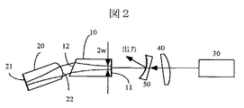
二つ目は図2に示すように面11から出力を取り出すもので、この場合、面21のコーティングは発振光に対して一部透過する反射コーティングにする。最適な透過率は使用する利得媒体により異なるが数%以下である。Cr:YAGレーザーの場合には0.5%程度のものを用いる。面21は高反射コーティングにする。面11から取り出した出力光は励起光と同一の光路を通るためダイクロイックミラー50により励起光の光路から分離する必要がある。ダイクロイックミラー50は励起光を透過し出力光を反射するミラーである。面11からの出力光は面11で最小ビーム径になっており出力後のビーム径は次第に広がる。したがってダイクロイックミラー50を凹面鏡にして出力光を平行光にすることが有利である。その場合、ダイクロイックミラー50は励起光に対しては凹レンズとして働きそれを考慮して収束レンズ40を選定する必要がある。凹レンズ50は励起光の光軸に対して垂直でないので非点収差を生じる。この非点収差は、特願平12-34306に開示のように、収束レンズ40を凹レンズ50の傾き方向と同方向又は逆方向に傾けることにより補償できる。
【0011】
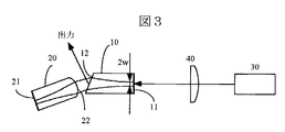
三つ目の方法は図3に示す通りで、面12を僅かにBrewster角からずらして研磨した場合、あるいは面12を垂直方向からある角度を持って研磨して僅かに無反射コーティングに反射成分を持たせた場合であり、面12を出力カプラにしている。この場合、面11と面12は発振光に対して高反射コーティングにする。
【0012】
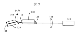
(実施例2)
実施例1に於いては利得媒体10は平面研磨し固体材料20の1つの面22を曲面研磨することによりレンズの機能を持たせ共振器の安定領域を形成した。逆に、固体材料120を平面研磨し、利得媒体110の一つの面112を曲面研磨しても安定な共振器を形成できる。それらを図示したものが図5、6、7である。図1、2、3と同様出力光の取り出しかたの違いで3つの図を示している。固体材料120の面122の研磨角度は実施例1の場合と同様に、Brewster角の場合、垂直研磨の場合、垂直方向からずらした角度の研磨の場合がある。利得媒体110の曲面112の曲率半径は、Cr:YAGレーザーの場合、例えば利得結晶長18mm、固体材料120として合成石英13mm、繰り返しレート2.4 GHzとすれば半径6mm程度に取れば良い。この曲率半径は実施例1の場合に比べて約2倍大きい。曲率半径は利得結晶110の面111でのビーム径が最適になるように決定する。実施例2では曲面によるレンズの位置が実施例1に比べて面111に近いので実施例1ほど短い焦点距離のレンズが必要なく面111の曲率半径が大きくて済む。この場合、球面収差が小さくなる、曲面研磨も容易になる、等の効果がある。
【0013】
その他、コーティングの方法、共振器内の非点収差の補正法、ダイクロイックミラー150の仕様、収束レンズ140の仕様等は実施例1の場合と同様である。
【0014】
(実施例3)
実施例1、2に於いては利得媒体又は固体材料の互いに向き合ったの面一つを曲面研磨することによりレンズの機能を持たせ共振器の安定領域を形成した。本実施例では図8、9に示すように利得媒体210及び固体材料220の両者の互いに向き合った面212、222を曲面研磨し安定な共振器を形成する。共振器内に曲面部を2つ設けたことで球面収差を軽減できる。出力光の取り出し方は2種類あり、固体材料220の面221から取り出す場合が図8であり、利得媒体210の面211から取り出す場合が図9である。各面のコーティングの方法は実施例1、2と同様である。図9の場合は実施例1、2と同様にダイクロイックミラー250により出力光を反射させる。ダイクロイックミラー250に凹面鏡を用いた場合は、励起光の非点収差を補償するために収束レンズ240を傾ける。
【0015】
図8、9では共に共振器内は回転対称になっている。回転対称の場合には発振光の偏波が安定しない場合があるが、実施例1、2と同様に発振光の光軸を共振器の回転中心軸からずらせば回転対称性がくずれ偏波を安定させることができる。
【0016】
(実施例4)
実施例1、2、3に於いては利得媒体と、それと逆の波長依存性を持った固体材料を対にして共振器を形成し、固体材料の長さを調整することにより共振器内の分散値を所為の値に設定した。本実施例では固体材料の代わりに、反射時に分散を生じるチャープミラーを用いる(図10、11)。チャープミラーを用いた固体レーザーの例は本願発明者らによる出願(特開平11-168252)に見られる。チャープミラーは誘電体又は半導体の多層膜で形成され、層厚を少しずつ変化させたもので分散を伴うミラーである(例えば、N. Matuschek, F.X. Krtner, and U. Keller, IEEE Journal of Quantum Electronics, Vol. 35, No. 2, pp. 129 - 137 (1999)艨j。分散の符号、大きさは層厚の制御で任意の値に設定でき、利得媒体の分散値に合わせて設計する。安定な共振器を形成するためには共振器内にレンズ機能が必要になるが、これは利得媒体310の面312を曲面研磨することにより達成する。出力光の取り出しかたは2種類あり、チャープミラー側から取り出すのが図10であり、利得媒体側から取り出すのが図11である。後者の場合にダイクロイックミラー350を用いるが、方法は実施例1、2、3と同様である。図10、11の共振器内は回転対称であり偏波が安定しない場合があるが、実施例3と同様に発振光の光軸を回転対称の軸からずらすことにより対称性を壊し偏波を安定させることができる。
【0017】
カーレンズモード同期可能な固体レーザーは自発的に超短パルス発振可能であるが、共振器内に可飽和吸収層を作りつければ超短パルス発振はさらに安定する。可飽和吸収層は光強度が強いときに透過率が高く、光強度が低いときに透過率が小さい性質を持つため、パルス部の光が存在する部分で透過率が高く、光の存在しないところで透過率が下がり、パルス発振を助長する働きがある。可飽和吸収層は半導体により作製されることも可能で(例えば、U. Keller, K.J. Weingarten, F.X. Krtner, D. Kopf, B. Braun, I.D. Jung, R. Fluck, C. H蔕nninger, N. Matuschek, and J.A. der Au, IEEE Journal of Selected Topics in Quantum Electronics, Vol. 2, No. 3, pp. 435 - 453 (1996))、チャープミラー360のチャープミラーコーティングの上に可飽和吸収層を積層すれば、つまり、チャープミラーの構造を分散を伴った多層膜反射コーティングと可飽和吸収層との積層構造にすれば、安定な超短パルス固体レーザーを作製できる。
【0018】
(実施例5)
超短パルス固体レーザーは広いスペクトルを有しており、これを波長毎に切り出せば波長多重光伝送用の多波長光源として用いることができる。それを具体的にブロック図で示したものが図12である。光伝送は通常1.5μ m帯の波長を用いるので、それに適当な固体レーザーはCr:YAGレーザーである。固体レーザー510の出力は、回折格子や導波路型回折格子(例えば、A, Kaneko, T. Goh, H. Yamada, T. Tanaka, and I. Ogawa, IEEE. Journal of Selected Topics in Quantum Electronics, Vol. 5, No. 5, pp. 1227 - 1236 (1999) )からなる分波器520に導かれ波長別に分離される。分離された各波長成分はそれぞれ個別の変調器に導かれ信号が乗せられる。変調された各波長成分は回折格子や導波路型回折格子からなる合波器540により合波され伝送される。以上の各部分をまとめて光送信機500が形成される。
【0019】
図12では合波器540により各波長成分が一つにまとめられ一個所に伝送されるが、ネットワーク管理の都合で波長別に伝送先が違う場合もある。その場合は図13に示すように合波器を設置せず、各々の波長別に出力すればよい。
【0020】
幹線系の光伝送では通常2.4 GHz又は10 GHzのビットレートを用いる。実施例1−4の超短パルス固体レーザーを用いればそのようなビットレートも可能であるが、共振器長が10 cmから数mの他の固体レーザーを用いた場合にはビットレートが小さくなる。その場合は図14、15に示すように固体レーザー510の出力を、パルスの繰り返しレートを整数倍する機能の時間多重器550に入力してビットレートを大きくする。時間多重器550から出力後は図12、13と同様である。
【0021】
時間多重器550の構成は色々なものがあり、代表的なものを図16−18に示す。図16は遅延線を用いた方法で、入力光を2つの光路551と552に分割しその後合波する。光路551と552は光路長が異なるので合波後はビットレートが2倍になる。光路553と554の対と、光路555と556の対も同様な働きをし、図15の時間多重器550は全体ではビットレートが8倍になる。
【0022】
図17は線形チャープファイバ回折格子557を用いた時間多重器550の例である。時間多重器550への入力光は光サーキュレータにより線形チャープファイバ回折格子557へ導かれる。線形チャープファイバ回折格子557ではチャープミラーと同様に分散を伴い反射される。その後光サーキュレータに再び戻って時間多重器から出力される。線形チャープファイバ回折格子557で設定する分散量は分散の結果パルス幅が広がり、隣り合うパルスが重なり合う程度に大きくする。分散量を適当な値に設定すればパルス同士の干渉の結果、ビットレートの大きくなったパルス列に変換される。分散量の設定の方法については文献(J. Azaa and M.A. Muriel, Optics Letters, Vol. 24, No. 23, pp. 1672 - 1674 (1999) jに記載されている。
【0023】
図17に於いてはパルス列に分散を与えるのに線形チャープファイバ回折格子557を用いたが、これは必ずしも線形チャープファイバ回折格子557である必要はなく所定の分散量を与えるものであればどのような分散媒体でも良い。これを図示したものが図18である。
【0024】
【発明の効果】
レンズの機能を、利得媒体又は固体材料に曲面研磨を施すことで達成し小型で高繰り返しレートの超短パルス固体レーザーを可能にする。また、固体レーザーを波長多重光伝送の送信機の光源に用いることにより、送信機における光源の数を大幅に減らすことができる。
【図面の簡単な説明】
【図1】本発明に関わる実施例1の固体レーザーの構成例の一つを示す図である。
【図2】本発明に関わる実施例1の固体レーザーの構成例の一つを示す図である。
【図3】本発明に関わる実施例1の固体レーザーの構成例の一つを示す図である。
【図4】図1、2、3の共振器部を拡大し、発振光の光軸を表わした図。
【図5】本発明に関わる実施例2の固体レーザーの構成例の一つを示す図である。
【図6】本発明に関わる実施例2の固体レーザーの構成例の一つを示す図である。
【図7】本発明に関わる実施例2の固体レーザーの構成例の一つを示す図である。
【図8】本発明に関わる実施例3の固体レーザーの構成例の一つを示す図である。
【図9】本発明に関わる実施例3の固体レーザーの構成例の一つを示す図である。
【図10】本発明に関わる実施例4の固体レーザーの構成例の一つを示す図である。
【図11】本発明に関わる実施例4の固体レーザーの構成例の一つを示す図である。
【図12】本発明に関わる実施例5の固体レーザーの構成例の一つを示す図である。
【図13】本発明に関わる実施例5の固体レーザーの構成例の一つを示す図である。
【図14】本発明に関わる実施例5の固体レーザーの構成例の一つを示す図である。
【図15】本発明に関わる実施例5の固体レーザーの構成例の一つを示す図である。
【図16】本発明に関わる実施例5の中の時間多重器550の構成例の一つを示す図である。
【図17】本発明に関わる実施例5の中の時間多重器550の構成例の一つを示す図である。
【図18】本発明に関わる実施例5の中の時間多重器550の構成例の一つを示す図である。
【符号の説明】
10:利得媒体、11:共振器のエンドミラーの働きをする利得媒体の一つの面、12:面11の反対側の面、20:分散材料、21:共振器のエンドミラーの働きをする分散材料の一つの面、22:面21の反対側の面、30:励起光源、40:収束レンズ、50:ダイクロイックミラー、
110:利得媒体、111:共振器のエンドミラーの働きをする利得媒体の一つの面、112:面111の反対側の面、120:分散材料、121:共振器のエンドミラーの働きをする分散材料の一つの面、122:面121の反対側の面、130:励起光源、140:収束レンズ、150:ダイクロイックミラー、
210:利得媒体、211:共振器のエンドミラーの働きをする利得媒体の一つの面、212:面211の反対側の面、220:分散材料、221:共振器のエンドミラーの働きをする分散材料の一つの面、222:面221の反対側の面、230:励起光源、240:収束レンズ、250:ダイクロイックミラー、
310:利得媒体、311:共振器のエンドミラーの働きをする利得媒体の一つの面、312:面311の反対側の面、330:励起光源、340:収束レンズ、350:ダイクロイックミラー、360:チャープミラー、
500:送信機、510:固体レーザー、520:分波器、530:変調器の一群、540:合波器、550:時間多重器、551:光路、552:光路、553:光路、554:光路、555:光路、556:光路、557:線形チャープファイバ回折格子、558:分散媒体、570:時間多重器550に入力前のパルス列、571:時間多重器550を出力後のパルス列。[0001]
BACKGROUND OF THE INVENTION
The present invention relates to an optical transmitter using a small solid laser and a solid laser.
[0002]
[Prior art]
With the rapid increase in demand for optical transmission capacity, the number of multiplexed lights in wavelength division multiplexing transmission is rapidly increasing. Currently, the number of wavelength multiplexing is ensured by arranging the number of semiconductor lasers as many as possible (for example, Hiroshi Toba, O plus E, Vol. 21, No. 8, pp. 965-974). However, if the number of multiplexing increases in the future, alternative means will be necessary from the viewpoint of cost, the size of the apparatus, the necessity of precise wavelength control, and the like.
[0003]
[Problems to be solved by the invention]
The problem in wavelength division multiplexing optical transmission is to reduce the number of light sources, reduce the cost, downsize the apparatus, and facilitate the wavelength control.
[0004]
[Means for Solving the Problems]
In order to answer this problem, in the present invention, an ultrashort pulse solid-state laser having a pulse width of 1 ps or less is used as the light source of the optical transmitter. Since the ultrashort pulse solid-state laser has a wide spectrum, many wavelength components necessary for wavelength multiplexing optical transmission can be extracted from one laser. Since the wavelength component of each channel is extracted from the output of the ultrashort pulse solid-state laser through a passive element, the wavelength control becomes easy. As a result, the cost is reduced and the apparatus is downsized. In order to use an ultrashort pulse solid-state laser as a multi-wavelength light source for wavelength multiplexing optical transmission, it is necessary to output a pulse train at a rate that matches the optical transmission rate. In trunk optical transmission, transmission is usually performed at a rate of 2.4 GHz or 10 GHz, but a general ultrashort pulse solid-state laser outputs a pulse train at a repetition rate of about 100 MHz. The ultrashort pulse laser has also been improved and recently a 1.2 GHz repetition rate (Tomaru et al., Opt. Lett. Vol. 25. In press.) Is possible, but higher repetition rates are required. In response to this need, the present invention produces a resonator consisting of only two points: a gain medium and a solid material or chirp mirror having a wavelength dependency opposite to that of the gain medium, thereby achieving miniaturization and high repetition. . When operating a solid-state laser with ultrashort pulses, it is necessary to set the dispersion value in the resonator to an appropriate value and to set the minimum beam diameter of the resonator mode in the gain medium to an appropriate value. The value can be set by adjusting the type and length of the solid material or the chirp amount of the chirp mirror, and the minimum beam diameter can be adjusted by the curvature of the curved surface polishing applied to the gain medium or solid material. This can be set.
[0005]
DETAILED DESCRIPTION OF THE INVENTION
(Example 1)
The configuration of this embodiment is shown in FIG. The resonator is composed of a
[0006]
In order to obtain a stable resonator, it is generally necessary to arrange a lens or a concave mirror as an element in the resonator and narrow the beam of oscillation light. In this embodiment, a stable resonator is obtained by polishing the
[0007]
The
[0008]
Excitation of the laser resonator is achieved by guiding the excitation light from the
[0009]
There are three ways to extract the output light from the resonator. The first is a method of taking out from the
[0010]
The second is to extract the output from the
[0011]
The third method is as shown in FIG. 3. When the
[0012]
(Example 2)
In the first embodiment, the
[0013]
In addition, the coating method, the astigmatism correction method in the resonator, the specification of the
[0014]
Example 3
In the first and second embodiments, one surface of the gain medium or solid material facing each other is subjected to curved surface polishing so as to have a lens function to form a stable region of the resonator. In this embodiment, as shown in FIGS. 8 and 9, the
[0015]
8 and 9, the inside of the resonator is rotationally symmetric. In the case of rotational symmetry, the polarization of the oscillation light may not be stable. However, if the optical axis of the oscillation light is shifted from the rotation center axis of the resonator as in the first and second embodiments, the rotational symmetry is lost and the polarization is changed. It can be stabilized.
[0016]
Example 4
In Examples 1, 2, and 3, a resonator is formed by pairing a gain medium and a solid material having a wavelength dependency opposite to that of the gain medium, and the length of the solid material is adjusted to adjust the length in the resonator. The variance value was set to the desired value. In this embodiment, a chirp mirror that generates dispersion upon reflection is used instead of a solid material (FIGS. 10 and 11). An example of a solid-state laser using a chirp mirror can be found in an application by the present inventors (Japanese Patent Laid-Open No. 11-168252). A chirped mirror is formed of a dielectric or semiconductor multilayer film, and is a mirror with dispersion by gradually changing the layer thickness (for example, N. Matuschek, FX Krtner, and U. Keller, IEEE Journal of Quantum Electronics , Vol. 35, No. 2, pp. 129-137 (1999) 艨 j. The sign and size of the dispersion can be set to any value by controlling the layer thickness, and designed according to the dispersion value of the gain medium. In order to form a stable resonator, a lens function is required in the resonator, which is achieved by polishing the
[0017]
The solid-state laser that can synchronize the car lens mode can spontaneously oscillate an ultrashort pulse, but if a saturable absorption layer is formed in the resonator, the ultrashort pulse oscillation is further stabilized. Since the saturable absorption layer has a property that the transmittance is high when the light intensity is strong and the transmittance is small when the light intensity is low, the transmittance is high in the portion where the light of the pulse portion exists, and the light does not exist. It has a function of reducing the transmittance and promoting pulse oscillation. The saturable absorber layer can also be made of a semiconductor (for example, U. Keller, KJ Weingarten, FX Krtner, D. Kopf, B. Braun, ID Jung, R. Fluck, C. H 蔕 nninger, N. Matuschek, and JA der Au, IEEE Journal of Selected Topics in Quantum Electronics, Vol. 2, No. 3, pp. 435-453 (1996)), stacking a saturable absorbing layer on the chirp mirror coating of
[0018]
(Example 5)
The ultrashort pulse solid-state laser has a wide spectrum, and if it is cut out for each wavelength, it can be used as a multi-wavelength light source for wavelength multiplexing optical transmission. This is specifically shown in a block diagram in FIG. Since the light transmission using the wavelength of the normal 1.5 mu m band, it suitable solid state laser is Cr: a YAG laser. The output of the solid-
[0019]
In FIG. 12, the wavelength components are combined into one by the
[0020]
For trunk line optical transmission, a bit rate of 2.4 GHz or 10 GHz is usually used. Such a bit rate is possible if the ultrashort pulse solid-state laser of Example 1-4 is used, but the bit rate decreases when other solid-state lasers having a resonator length of 10 cm to several m are used. . In this case, as shown in FIGS. 14 and 15, the output of the solid-
[0021]
There are various configurations of the
[0022]
FIG. 17 shows an example of a
[0023]
In FIG. 17, the linear chirped
[0024]
【The invention's effect】
The lens function is achieved by subjecting the gain medium or solid material to curved polishing, enabling a compact, high repetition rate ultrashort pulse solid state laser. Moreover, the number of light sources in the transmitter can be greatly reduced by using a solid-state laser as the light source of the transmitter for wavelength division multiplexing optical transmission.
[Brief description of the drawings]
FIG. 1 is a diagram showing one configuration example of a solid-state laser of Example 1 according to the present invention.
FIG. 2 is a diagram showing one configuration example of the solid-state laser according to the first embodiment of the present invention.
FIG. 3 is a diagram showing one configuration example of the solid-state laser according to the first embodiment of the present invention.
FIG. 4 is an enlarged view of the resonator unit shown in FIGS. 1, 2, and 3, and represents the optical axis of oscillation light.
FIG. 5 is a diagram showing one configuration example of a solid-state laser according to a second embodiment related to the present invention.
FIG. 6 is a diagram showing one configuration example of a solid-state laser according to a second embodiment related to the present invention.
FIG. 7 is a diagram showing one configuration example of a solid-state laser according to a second embodiment of the present invention.
FIG. 8 is a diagram showing one configuration example of a solid-state laser according to a third embodiment of the present invention.
FIG. 9 is a diagram showing one configuration example of a solid-state laser according to a third embodiment of the present invention.
FIG. 10 is a diagram showing one configuration example of a solid-state laser according to a fourth embodiment of the present invention.
FIG. 11 is a diagram showing one configuration example of a solid-state laser of Example 4 according to the present invention.
FIG. 12 is a diagram showing one configuration example of a solid-state laser according to a fifth embodiment of the present invention.
FIG. 13 is a view showing one configuration example of a solid-state laser according to a fifth embodiment of the present invention.
FIG. 14 is a diagram showing one configuration example of a solid-state laser according to a fifth embodiment of the invention.
FIG. 15 is a diagram showing one configuration example of a solid-state laser according to a fifth embodiment of the invention.
FIG. 16 is a diagram showing one configuration example of a
FIG. 17 is a diagram showing one configuration example of a
FIG. 18 is a diagram showing one configuration example of a
[Explanation of symbols]
10: gain medium, 11: one surface of gain medium acting as an end mirror of the resonator, 12: surface opposite to the
110: gain medium, 111: one surface of the gain medium that functions as an end mirror of the resonator, 112: a surface opposite to the
210: gain medium, 211: one surface of the gain medium that functions as an end mirror of the resonator, 212: a surface opposite to the
310: gain medium, 311: one surface of the gain medium serving as an end mirror of the resonator, 312: a surface opposite to the
500: transmitter, 510: solid state laser, 520: duplexer, 530: modulator group, 540: multiplexer, 550: time multiplexer, 551: optical path, 552: optical path, 553: optical path, 554: optical path 555: optical path, 556: optical path, 557: linear chirped fiber diffraction grating, 558: dispersion medium, 570: pulse train before input to the
Claims (18)
Priority Applications (6)
| Application Number | Priority Date | Filing Date | Title |
|---|---|---|---|
| JP2000107973A JP3858563B2 (en) | 2000-04-05 | 2000-04-05 | Solid-state laser capable of car lens mode synchronization |
| CA002319892A CA2319892A1 (en) | 2000-04-05 | 2000-09-15 | Solid-state laser and optical transmitter |
| US09/665,619 US6560267B1 (en) | 2000-04-05 | 2000-09-19 | Solid-state laser and optical transmitter |
| EP00120122A EP1143581A3 (en) | 2000-04-05 | 2000-09-19 | Solid-state laser and optical transmitter |
| CN00128674.9A CN1316809A (en) | 2000-04-05 | 2000-09-20 | Solid-state laser and optical transmitting machine |
| US10/420,902 US6754248B2 (en) | 2000-04-05 | 2003-04-23 | Solid-state laser and optical transmitter |
Applications Claiming Priority (1)
| Application Number | Priority Date | Filing Date | Title |
|---|---|---|---|
| JP2000107973A JP3858563B2 (en) | 2000-04-05 | 2000-04-05 | Solid-state laser capable of car lens mode synchronization |
Publications (3)
| Publication Number | Publication Date |
|---|---|
| JP2001291918A JP2001291918A (en) | 2001-10-19 |
| JP2001291918A5 JP2001291918A5 (en) | 2004-12-16 |
| JP3858563B2 true JP3858563B2 (en) | 2006-12-13 |
Family
ID=18620894
Family Applications (1)
| Application Number | Title | Priority Date | Filing Date |
|---|---|---|---|
| JP2000107973A Expired - Fee Related JP3858563B2 (en) | 2000-04-05 | 2000-04-05 | Solid-state laser capable of car lens mode synchronization |
Country Status (5)
| Country | Link |
|---|---|
| US (2) | US6560267B1 (en) |
| EP (1) | EP1143581A3 (en) |
| JP (1) | JP3858563B2 (en) |
| CN (1) | CN1316809A (en) |
| CA (1) | CA2319892A1 (en) |
Families Citing this family (14)
| Publication number | Priority date | Publication date | Assignee | Title |
|---|---|---|---|---|
| JP3858563B2 (en) * | 2000-04-05 | 2006-12-13 | 株式会社日立製作所 | Solid-state laser capable of car lens mode synchronization |
| US7453486B2 (en) * | 2000-12-13 | 2008-11-18 | Orbotech Ltd | Pulse light pattern writer |
| WO2003028177A1 (en) * | 2001-09-24 | 2003-04-03 | Giga Tera Ag | Pulse-generating laser |
| US20030058904A1 (en) * | 2001-09-24 | 2003-03-27 | Gigatera Ag | Pulse-generating laser |
| KR100442658B1 (en) * | 2002-08-14 | 2004-08-02 | 삼성전자주식회사 | Light source device for wavelength division multiplexing optical communication system |
| JP2008028379A (en) * | 2006-06-22 | 2008-02-07 | Fujifilm Corp | Mode-locked laser device |
| EP1870972A1 (en) * | 2006-06-22 | 2007-12-26 | Fujifilm Corporation | Mode-locked laser device |
| AT505021B1 (en) * | 2006-06-27 | 2008-10-15 | Nxp Semiconductors Austria Gmb | MEMBRANLESS MICROPHONE WITH THE HELP OF LIGHT INTERFERENCE |
| JP2010045147A (en) * | 2008-08-12 | 2010-02-25 | Fujifilm Corp | Mode synchronous laser device, pulse laser light source device, and microscope device |
| JP2010103291A (en) * | 2008-10-23 | 2010-05-06 | Fujifilm Corp | Mode synchronous laser device |
| US10333266B2 (en) | 2013-10-25 | 2019-06-25 | Alta Lasers As | Graphene-based optical sub-system |
| US9851570B2 (en) | 2014-09-18 | 2017-12-26 | Ipg Photonics Corporation | Beam shaping of high intensity high frequency optical output |
| WO2017175344A1 (en) * | 2016-04-07 | 2017-10-12 | ギガフォトン株式会社 | Solid-state laser device, solid-state laser system, and laser device for light exposure device |
| CN105932534A (en) * | 2016-06-17 | 2016-09-07 | 北京国科世纪激光技术有限公司 | Intracavity frequency doubling astigmatism compensation type laser |
Family Cites Families (12)
| Publication number | Priority date | Publication date | Assignee | Title |
|---|---|---|---|---|
| US5212698A (en) * | 1990-05-02 | 1993-05-18 | Spectra-Physics Lasers, Incorporated | Dispersion compensation for ultrashort pulse generation in tuneable lasers |
| US5856996A (en) * | 1992-12-07 | 1999-01-05 | The United States Of America As Represented By The Secretary Of The Air Force | Compact efficient solid state laser |
| WO1995031023A1 (en) * | 1994-05-09 | 1995-11-16 | Massachusetts Institute Of Technology | Dispersion-compensated laser using prismatic end elements |
| US5586996A (en) | 1994-05-12 | 1996-12-24 | Manookian, Jr.; Arman K. | Vapor separating device |
| US5761227A (en) * | 1994-08-23 | 1998-06-02 | Laser Power Corporation | Efficient frequency-converted laser |
| DE19603637C1 (en) * | 1996-02-01 | 1997-07-31 | Lambda Physik Gmbh | Narrow band radiation emitting laser |
| US5912915A (en) * | 1997-05-19 | 1999-06-15 | Coherent, Inc. | Ultrafast laser with multiply-folded resonant cavity |
| JPH11168252A (en) | 1997-12-05 | 1999-06-22 | Hitachi Ltd | Small solid-state laser |
| US6229835B1 (en) * | 1997-12-05 | 2001-05-08 | Hitachi, Ltd. | Compact solid-state laser and transmitter using the same |
| US6393037B1 (en) * | 1999-02-03 | 2002-05-21 | Lambda Physik Ag | Wavelength selector for laser with adjustable angular dispersion |
| US6393035B1 (en) * | 1999-02-01 | 2002-05-21 | Gigatera Ag | High-repetition rate passively mode-locked solid-state laser |
| JP3858563B2 (en) * | 2000-04-05 | 2006-12-13 | 株式会社日立製作所 | Solid-state laser capable of car lens mode synchronization |
-
2000
- 2000-04-05 JP JP2000107973A patent/JP3858563B2/en not_active Expired - Fee Related
- 2000-09-15 CA CA002319892A patent/CA2319892A1/en not_active Abandoned
- 2000-09-19 US US09/665,619 patent/US6560267B1/en not_active Expired - Fee Related
- 2000-09-19 EP EP00120122A patent/EP1143581A3/en not_active Withdrawn
- 2000-09-20 CN CN00128674.9A patent/CN1316809A/en active Pending
-
2003
- 2003-04-23 US US10/420,902 patent/US6754248B2/en not_active Expired - Fee Related
Also Published As
| Publication number | Publication date |
|---|---|
| EP1143581A2 (en) | 2001-10-10 |
| CN1316809A (en) | 2001-10-10 |
| JP2001291918A (en) | 2001-10-19 |
| US20030210730A1 (en) | 2003-11-13 |
| US6754248B2 (en) | 2004-06-22 |
| US6560267B1 (en) | 2003-05-06 |
| EP1143581A3 (en) | 2004-09-15 |
| CA2319892A1 (en) | 2001-10-05 |
Similar Documents
| Publication | Publication Date | Title |
|---|---|---|
| JP3858563B2 (en) | Solid-state laser capable of car lens mode synchronization | |
| US8005122B2 (en) | Mode-locked laser | |
| US6055261A (en) | Ultrafast laser with multiply-folded resonant cavity | |
| US4797893A (en) | Microlaser system | |
| US8130802B2 (en) | Tunable laser | |
| US20060251132A1 (en) | Ultrashort pulsed laser and optical head using the same | |
| US6256434B1 (en) | Method and dielectric and/or semiconductor device for influencing the dispersion of electromagnetic radiation | |
| US6940879B2 (en) | External cavity laser with dispersion compensation for mode-hop-free tuning | |
| WO2007007848A1 (en) | External resonator variable wavelength laser and its packaging method | |
| JPH11168252A (en) | Small solid-state laser | |
| JP2001291918A5 (en) | ||
| US6351484B1 (en) | Output couplers for lasers | |
| US6498799B1 (en) | Single-mode fiber ring laser | |
| EP2218150B1 (en) | Phase stabilized mode-locked laser with two output couplers having different spectral transmission | |
| JP2004165652A (en) | Ultrashort pulsed laser device and optical head using the same | |
| US20220255284A1 (en) | Tunable external cavity laser with dual gain chips | |
| JPS616888A (en) | External resonator type semiconductor laser device | |
| Jacobsson et al. | Widely Tunable Yb: KYW Laser Locked by a Volume Bragg Grating | |
| JPH1051051A (en) | Ring laser equipment | |
| JP2001284688A (en) | Optical amplifier | |
| JP2000012930A (en) | Laser resonator |
Legal Events
| Date | Code | Title | Description |
|---|---|---|---|
| A521 | Request for written amendment filed |
Free format text: JAPANESE INTERMEDIATE CODE: A523 Effective date: 20040109 |
|
| A621 | Written request for application examination |
Free format text: JAPANESE INTERMEDIATE CODE: A621 Effective date: 20040109 |
|
| A977 | Report on retrieval |
Free format text: JAPANESE INTERMEDIATE CODE: A971007 Effective date: 20050623 |
|
| RD01 | Notification of change of attorney |
Free format text: JAPANESE INTERMEDIATE CODE: A7421 Effective date: 20060417 |
|
| A131 | Notification of reasons for refusal |
Free format text: JAPANESE INTERMEDIATE CODE: A131 Effective date: 20060516 |
|
| A521 | Request for written amendment filed |
Free format text: JAPANESE INTERMEDIATE CODE: A523 Effective date: 20060622 |
|
| TRDD | Decision of grant or rejection written | ||
| A01 | Written decision to grant a patent or to grant a registration (utility model) |
Free format text: JAPANESE INTERMEDIATE CODE: A01 Effective date: 20060829 |
|
| A61 | First payment of annual fees (during grant procedure) |
Free format text: JAPANESE INTERMEDIATE CODE: A61 Effective date: 20060911 |
|
| FPAY | Renewal fee payment (event date is renewal date of database) |
Free format text: PAYMENT UNTIL: 20090929 Year of fee payment: 3 |
|
| FPAY | Renewal fee payment (event date is renewal date of database) |
Free format text: PAYMENT UNTIL: 20100929 Year of fee payment: 4 |
|
| FPAY | Renewal fee payment (event date is renewal date of database) |
Free format text: PAYMENT UNTIL: 20100929 Year of fee payment: 4 |
|
| FPAY | Renewal fee payment (event date is renewal date of database) |
Free format text: PAYMENT UNTIL: 20110929 Year of fee payment: 5 |
|
| FPAY | Renewal fee payment (event date is renewal date of database) |
Free format text: PAYMENT UNTIL: 20120929 Year of fee payment: 6 |
|
| FPAY | Renewal fee payment (event date is renewal date of database) |
Free format text: PAYMENT UNTIL: 20120929 Year of fee payment: 6 |
|
| FPAY | Renewal fee payment (event date is renewal date of database) |
Free format text: PAYMENT UNTIL: 20130929 Year of fee payment: 7 |
|
| LAPS | Cancellation because of no payment of annual fees |