US6256434B1 - Method and dielectric and/or semiconductor device for influencing the dispersion of electromagnetic radiation - Google Patents
Method and dielectric and/or semiconductor device for influencing the dispersion of electromagnetic radiation Download PDFInfo
- Publication number
- US6256434B1 US6256434B1 US09/352,248 US35224899A US6256434B1 US 6256434 B1 US6256434 B1 US 6256434B1 US 35224899 A US35224899 A US 35224899A US 6256434 B1 US6256434 B1 US 6256434B1
- Authority
- US
- United States
- Prior art keywords
- substrate
- electromagnetic radiation
- multilayer structure
- index
- coating
- Prior art date
- Legal status (The legal status is an assumption and is not a legal conclusion. Google has not performed a legal analysis and makes no representation as to the accuracy of the status listed.)
- Expired - Lifetime
Links
Images


Classifications
-
- H—ELECTRICITY
- H01—ELECTRIC ELEMENTS
- H01S—DEVICES USING THE PROCESS OF LIGHT AMPLIFICATION BY STIMULATED EMISSION OF RADIATION [LASER] TO AMPLIFY OR GENERATE LIGHT; DEVICES USING STIMULATED EMISSION OF ELECTROMAGNETIC RADIATION IN WAVE RANGES OTHER THAN OPTICAL
- H01S3/00—Lasers, i.e. devices using stimulated emission of electromagnetic radiation in the infrared, visible or ultraviolet wave range
- H01S3/05—Construction or shape of optical resonators; Accommodation of active medium therein; Shape of active medium
- H01S3/06—Construction or shape of active medium
- H01S3/0627—Construction or shape of active medium the resonator being monolithic, e.g. microlaser
-
- G—PHYSICS
- G02—OPTICS
- G02B—OPTICAL ELEMENTS, SYSTEMS OR APPARATUS
- G02B1/00—Optical elements characterised by the material of which they are made; Optical coatings for optical elements
- G02B1/10—Optical coatings produced by application to, or surface treatment of, optical elements
- G02B1/11—Anti-reflection coatings
- G02B1/113—Anti-reflection coatings using inorganic layer materials only
- G02B1/115—Multilayers
-
- H—ELECTRICITY
- H01—ELECTRIC ELEMENTS
- H01S—DEVICES USING THE PROCESS OF LIGHT AMPLIFICATION BY STIMULATED EMISSION OF RADIATION [LASER] TO AMPLIFY OR GENERATE LIGHT; DEVICES USING STIMULATED EMISSION OF ELECTROMAGNETIC RADIATION IN WAVE RANGES OTHER THAN OPTICAL
- H01S3/00—Lasers, i.e. devices using stimulated emission of electromagnetic radiation in the infrared, visible or ultraviolet wave range
- H01S3/005—Optical devices external to the laser cavity, specially adapted for lasers, e.g. for homogenisation of the beam or for manipulating laser pulses, e.g. pulse shaping
- H01S3/0057—Temporal shaping, e.g. pulse compression, frequency chirping
-
- G—PHYSICS
- G02—OPTICS
- G02B—OPTICAL ELEMENTS, SYSTEMS OR APPARATUS
- G02B6/00—Light guides; Structural details of arrangements comprising light guides and other optical elements, e.g. couplings
- G02B6/24—Coupling light guides
- G02B6/26—Optical coupling means
- G02B6/28—Optical coupling means having data bus means, i.e. plural waveguides interconnected and providing an inherently bidirectional system by mixing and splitting signals
- G02B6/293—Optical coupling means having data bus means, i.e. plural waveguides interconnected and providing an inherently bidirectional system by mixing and splitting signals with wavelength selective means
- G02B6/29346—Optical coupling means having data bus means, i.e. plural waveguides interconnected and providing an inherently bidirectional system by mixing and splitting signals with wavelength selective means operating by wave or beam interference
- G02B6/29361—Interference filters, e.g. multilayer coatings, thin film filters, dichroic splitters or mirrors based on multilayers, WDM filters
-
- G—PHYSICS
- G02—OPTICS
- G02B—OPTICAL ELEMENTS, SYSTEMS OR APPARATUS
- G02B6/00—Light guides; Structural details of arrangements comprising light guides and other optical elements, e.g. couplings
- G02B6/24—Coupling light guides
- G02B6/26—Optical coupling means
- G02B6/28—Optical coupling means having data bus means, i.e. plural waveguides interconnected and providing an inherently bidirectional system by mixing and splitting signals
- G02B6/293—Optical coupling means having data bus means, i.e. plural waveguides interconnected and providing an inherently bidirectional system by mixing and splitting signals with wavelength selective means
- G02B6/29379—Optical coupling means having data bus means, i.e. plural waveguides interconnected and providing an inherently bidirectional system by mixing and splitting signals with wavelength selective means characterised by the function or use of the complete device
- G02B6/29392—Controlling dispersion
- G02B6/29394—Compensating wavelength dispersion
-
- H—ELECTRICITY
- H01—ELECTRIC ELEMENTS
- H01S—DEVICES USING THE PROCESS OF LIGHT AMPLIFICATION BY STIMULATED EMISSION OF RADIATION [LASER] TO AMPLIFY OR GENERATE LIGHT; DEVICES USING STIMULATED EMISSION OF ELECTROMAGNETIC RADIATION IN WAVE RANGES OTHER THAN OPTICAL
- H01S3/00—Lasers, i.e. devices using stimulated emission of electromagnetic radiation in the infrared, visible or ultraviolet wave range
- H01S3/05—Construction or shape of optical resonators; Accommodation of active medium therein; Shape of active medium
- H01S3/06—Construction or shape of active medium
- H01S3/0602—Crystal lasers or glass lasers
- H01S3/0606—Crystal lasers or glass lasers with polygonal cross-section, e.g. slab, prism
-
- H—ELECTRICITY
- H01—ELECTRIC ELEMENTS
- H01S—DEVICES USING THE PROCESS OF LIGHT AMPLIFICATION BY STIMULATED EMISSION OF RADIATION [LASER] TO AMPLIFY OR GENERATE LIGHT; DEVICES USING STIMULATED EMISSION OF ELECTROMAGNETIC RADIATION IN WAVE RANGES OTHER THAN OPTICAL
- H01S3/00—Lasers, i.e. devices using stimulated emission of electromagnetic radiation in the infrared, visible or ultraviolet wave range
- H01S3/05—Construction or shape of optical resonators; Accommodation of active medium therein; Shape of active medium
- H01S3/06—Construction or shape of active medium
- H01S3/0619—Coatings, e.g. AR, HR, passivation layer
- H01S3/0621—Coatings on the end-faces, e.g. input/output surfaces of the laser light
-
- H—ELECTRICITY
- H01—ELECTRIC ELEMENTS
- H01S—DEVICES USING THE PROCESS OF LIGHT AMPLIFICATION BY STIMULATED EMISSION OF RADIATION [LASER] TO AMPLIFY OR GENERATE LIGHT; DEVICES USING STIMULATED EMISSION OF ELECTROMAGNETIC RADIATION IN WAVE RANGES OTHER THAN OPTICAL
- H01S3/00—Lasers, i.e. devices using stimulated emission of electromagnetic radiation in the infrared, visible or ultraviolet wave range
- H01S3/05—Construction or shape of optical resonators; Accommodation of active medium therein; Shape of active medium
- H01S3/08—Construction or shape of optical resonators or components thereof
- H01S3/08059—Constructional details of the reflector, e.g. shape
-
- H—ELECTRICITY
- H01—ELECTRIC ELEMENTS
- H01S—DEVICES USING THE PROCESS OF LIGHT AMPLIFICATION BY STIMULATED EMISSION OF RADIATION [LASER] TO AMPLIFY OR GENERATE LIGHT; DEVICES USING STIMULATED EMISSION OF ELECTROMAGNETIC RADIATION IN WAVE RANGES OTHER THAN OPTICAL
- H01S3/00—Lasers, i.e. devices using stimulated emission of electromagnetic radiation in the infrared, visible or ultraviolet wave range
- H01S3/05—Construction or shape of optical resonators; Accommodation of active medium therein; Shape of active medium
- H01S3/08—Construction or shape of optical resonators or components thereof
- H01S3/08095—Zig-zag travelling beam through the active medium
-
- H—ELECTRICITY
- H01—ELECTRIC ELEMENTS
- H01S—DEVICES USING THE PROCESS OF LIGHT AMPLIFICATION BY STIMULATED EMISSION OF RADIATION [LASER] TO AMPLIFY OR GENERATE LIGHT; DEVICES USING STIMULATED EMISSION OF ELECTROMAGNETIC RADIATION IN WAVE RANGES OTHER THAN OPTICAL
- H01S5/00—Semiconductor lasers
- H01S5/005—Optical components external to the laser cavity, specially adapted therefor, e.g. for homogenisation or merging of the beams or for manipulating laser pulses, e.g. pulse shaping
- H01S5/0057—Optical components external to the laser cavity, specially adapted therefor, e.g. for homogenisation or merging of the beams or for manipulating laser pulses, e.g. pulse shaping for temporal shaping, e.g. pulse compression, frequency chirping
-
- H—ELECTRICITY
- H01—ELECTRIC ELEMENTS
- H01S—DEVICES USING THE PROCESS OF LIGHT AMPLIFICATION BY STIMULATED EMISSION OF RADIATION [LASER] TO AMPLIFY OR GENERATE LIGHT; DEVICES USING STIMULATED EMISSION OF ELECTROMAGNETIC RADIATION IN WAVE RANGES OTHER THAN OPTICAL
- H01S5/00—Semiconductor lasers
- H01S5/02—Structural details or components not essential to laser action
- H01S5/028—Coatings ; Treatment of the laser facets, e.g. etching, passivation layers or reflecting layers
Definitions
- the invention relates to the field of reflective dielectric and/or semiconductor devices, and more particularly to broadband reflective dielectric and/or semiconductor devices used as mirrors in laser resonators.
- a chirped mirror The basic idea behind a chirped mirror is relatively simple: layers with increasing thicknesses (e.g., quarter-wave layers with a gradually increasing Bragg wavelength) are stacked such that longer wavelengths penetrate deeper into the mirror structure, producing a negative group delay dispersion (GDD). The whole principle can also be inverted by decreasing the layer thicknesses, which results in chirped mirrors with a positive GDD.
- layers with increasing thicknesses e.g., quarter-wave layers with a gradually increasing Bragg wavelength
- GDD group delay dispersion
- chirped mirrors have one major disadvantage, as far as has been demonstrated.
- the designed group delay (GD) and GDD generally show unwanted oscillations around their desired target functions.
- GD group delay
- GDD group delay
- these oscillations are reduced as much as possible by more or less sophisticated numerical optimization techniques (R. Szipöcs, K. Ferencz, Ch. Spielmann, and F. Krausz, Opt. Lett. 19, 201, (1994); G. Tempea, F. Krausz, Ch. Spielmann, and K. Ferencz, IEEE JSTQE 4, 193, (1997); R. Szipöcs, and A. Kohazi-Kis, Apl.
- a GTI is formed due to an impedance mismatch of the designed stricture to the theoretically assumed refractive index of the ambient medium.
- the matching problem b) does not exist.
- the matching problem b) also does not exist, if the refractive index of the ambient medium is identical to the theoretically assumed index for the ambient medium.
- the assumed refractive index can have any value that is appropriate for the generation of the theoretical design. From the theoretical point of view, for the case of a binary multilayer system, promising candidates are the refractive index of the low- or high-index layer, the arithmetic or geometric average refractive index, or the effective refractive index. However, the choice is not limited to these indices.
- a typical solution for problem b) is a multilayer subsection, which acts as an antireflection (AR) coating, that matches the theoretically assumed refractive index to the index of the ambient medium.
- a double-chirped mirror is a multilayer interference coating that can be considered as a composition of four sections.
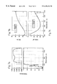
- FIG. 1 is a schematic drawing of a standard DCM 101 according to the prior art, composed of four multilayer sections 104 , 131 - 133 deposited on a substrate 102 . Each of the sections 104 , 131 - 133 serves a different task (see, e.g., N. Matuschek, F. X. Kärtner, and U. Keller, IEEE J. Quantum Electron. 35, 129 (1999)).
- the first section 104 is a broadband AR coating, typically consisting of 10-14 layers (not shown separately). This AR coating 104 solves the matching problem b), as mentioned above.
- Double-chirping means that, in addition to the local Bragg wavelength, the local coupling of an incident electromagnetic wave to a reflected electromagnetic wave is independently chirped. This corresponds to an adiabatic matching of the impedance. In terms of optical thicknesses, this means that for a fixed Bragg wavelength, the coupling strength is independently increased by increasing the duty cycle of the high-index layer from layer pair to layer pair from zero to 0.5.
- duty cycle denotes the ratio of the optical thickness of the low-index layer 103 . 11 or high-index layer 103 . 21 to the optical thickness of the whole layer pair 103 . 11 , 103 . 21 .
- the same impedance matching is achieved by inverse double-chirping, i.e., the duty cycle of the low-index layer is increased for a fixed Bragg wavelength.
- the AR-coating section 104 has to match from air 105 to the index of the high-index layer.
- a simple-chirp section 132 only the Bragg wavelength is chirped, whereas in a quarter-wave section 133 the Bragg wavelength is kept constant.
- This method produces a high reflectance for the long wavelengths (F. X. Kärtner, N. Matuschek, T. Schibli, U. Keller, H. Haus, C. Heine, R. Morf, V. Scheuer, M. Tilsch and T. Tschudi, Opt. Lett.
- the bandwidth is limited to about 240 nm (680-920 nm) (see FIG. 6 ( a ) dashed line, and N. Matuschek, F. X. Kärtner, and U. Keller, IEEE J Sel. Topics Quantum Electron. 4, 197 (1998)).
- This bandwidth gives a good estimate for the bandwidth of a DCM with relatively small oscillations in the GDD.
- the invention discloses a way for almost completely avoiding oscillations in the GDD.
- the layers are coated on the back side of a substrate with a refractive index equal or close to the theoretically assumed refractive index of the ambient medium.
- the refractive index of the substrate should be close to the index of the low-index layer (or high-index layer if the structure is inversely double-chirped).
- An almost perfect impedance matching of the double-chirp section and the substrate can be achieved if the low-index layer consists of sputtered SiO 2 and the substrate is made of fused silica.
- BASIC chirped mirrors we call chirped mirror structures, which are coated on the back side of the substrate, back-side coated chirped mirrors (BASIC chirped mirrors).
- BASIC chirped mirrors back-side coated chirped mirrors
- the substrate is treated as a non-interfering thick layer.
- the condition of a non-interfering substrate layer is fulfilled if the substrate is sufficiently thick, i.e., much thicker than the spatial extension of the light pulse. Additionally, the front side must not be parallel to the back side of the substrate. This can be accomplished either by wedging of the substrate or by choosing different centers of curvature for both sides.
- a light pulse reflected by a BASIC chirped mirror has to pass the AR coating (if there is one coated on the front side) and the substrate, is reflected by the chirped mirror structure, and passes the substrate and AR coating once again.
- the total GDD of a BASIC chirped mirror (including an AR coating) for one bounce is given by the GDD upon reflection of the theoretical DCM structure and two times the GDD upon transmission of the AR coating and the substrate.
- the thicker the substrate the more positive GDD is added to the negative GDD of the theoretical DCM structure because of the positive material dispersion.
- the substrate is too thin the stability of the coating is reduced and the surface might become distorted.
- the basic idea of the invention is the use of a back-side coating to provide impedance matching and thus to suppress GD and GDD oscillations of a chirped mirror structure.
- a chirped mirror any mirror structure that provides a controlled dispersion characteristic is meant.
- back-side coating on a substrate means any realization of a chirped mirror structure, where the incident light travels through a non-interfering thick layer (bulk material).
- this thick layer the “substrate”.
- An example for another realization is that the chirped mirror structure is surrounded on both ends by a thick layer, from which one can be called substrate.
- the idea of using substrate materials for achieving impedance matching covers any realization in which a chirped mirror structure is designed assuming a refractive index for the ambient medium which is different from the index of the actual ambient medium. This covers also the case if the actual ambient medium is not air but any other material.
- An important extension of the functionality of the BASIC chirped mirror is an AR coating on the opposite side of the substrate. However, it is important that the reflection of this coating does not interfere with the reflection of the back-side coating. For the invention, the AR coating is not necessarily required. Computer optimization or complete generation of the coating design significantly enhances the performance.
- FIG. 1 is a schematic drawing of a standard double-chirped mirror (DCM) according to the prior art.
- FIG. 2 a is a schematic drawing of a first embodiment of a backside coated chirped mirror (BASIC chirped mirror) according to the invention, namely a BASIC single-chirped mirror (SCM).
- BASIC chirped mirror backside coated chirped mirror
- FIG. 2 b is a schematic drawing of a second embodiment of a backside coated chirped mirror (BASIC chirped mirror) according to the invention, namely a BASIC double-chirped mirror (DCM).
- BASIC chirped mirror backside coated chirped mirror
- FIG. 3 a shows the reflectance calculated for two BASIC chirped mirror structures according to the invention.
- FIG. 3 b shows the group delay (GD) calculated for two BASIC chirped mirror structures according to the invention.
- two BASIC chirped mirror structures according to the invention It is assumed that the refractive index of the substrate is equal to the refractive index of the low-index material.
- FIG. 4 a shows the reflectance calculated for two BASIC chirped mirror structures according to the invention.
- FIG. 4 b shows the GD calculated for two BASIC chirped mirror structures according to the invention. In contrast to FIGS. 3 a and 3 b, it is assumed that the refractive index of the substrate is equal to the refractive index of the high-index material.
- FIG. 5 a shows the reflectance calculated for two BASIC SCM structures according to the invention.
- FIG. 6 a shows a reflectance calculated for an 18-layer AR coating on the front side of a fused silica substrate, and, with a dashed line, the reflectance of an AR coating of a standard DCM according to the state of the art is shown,
- FIG. 6 b shows a global transmittance calculated for an 18-layer AR coating on the front side of a fused silica substrate.
- FIG. 7 a shows the reflectance calculated for a 60-layer DCM structure on the back side of the fused silica substrate according to the invention.
- FIG. 7 b shows the GD upon reflection calculated for a 60-layer DCM structure on the back side of the fused silica substrate according to the invention.
- FIG. 7 c shows the GDD upon reflection calculated for a 60-layer DCM structure on the back side of the fused silica substrate according to the invention.
- the dispersion of the coating only has been shown; the dispersion of the substrate has not been added.
- the dashed line represents the desired target GD and GDD, respectively.
- FIG. 8 a shows the calculated differences between the designed and desired GD.
- FIG. 8 b shows the calculated differences between the designed and desired GDD.
- the solid lines show results for the BASIC-DCM according to the invention, and the dashed lines for a standard DCM according to the state of the art.
- FIG. 9 a shows the measured GDD; the the dotted line represents the desired GDD of a theoretical DCM structure (without substrate and AR coating) coated on the back side of a substrate.
- the dash-dotted and dashed lines show the desired GDD upon transmission of the substrate and the AR coating is added to the dotted curve, for two different substrate thicknesses.
- FIG. 9 b shows the difference between the measured and desired target GDD; the result of a typical GDD measurement for a BASIC-DCM according to the invention (solid line) is compared with the result for an ultra broadband standard DCM according to the state of the art (dashed line). upon transmission of the substrate and the AR coating is added to the dotted curve, for two different substrate thicknesses.
- the result of a typical GDD measurement for a BASIC-DCM according to the invention (solid line) is compared with the result for an ultrabroadband standard DCM according to the state of the art (dashed line).
- FIG. 10 is a schematic drawing of a BASIC chirped mirror on a wedged substrate.
- FIG. 11 is a schematic drawing of a BASIC chirped mirror on a thin lens substrate.
- FIG. 12 is a schematic drawing of a BASIC chirped mirror on a semicylindrical or a semispherical substrate.
- FIG. 13 is a schematic drawing of a modified prism pair, one of the prisms bearing a BASIC chirped mirror.
- FIG. 14 is a schematic drawing of a BASIC chirped mirror on a half Brewster prism.
- FIG. 15 is a schematic drawing of a BASIC chirped mirror on a wedged substrate.
- FIGS. 16-17 are schematic drawings of three embodiments of a laser cavity with a laser slab crystal bearing BASIC chirped mirrors on two parallel sides.
- FIGS. 18 and 19 are schematic drawings of two embodiments of a microchip laser bearing BASIC chirped mirrors on two facets.
- FIGS. 2 a and 2 b are schematic drawings of two embodiments of back-side coated chirped mirrors 1 (BASIC chirped mirrors) according to the invention.
- a chirped-mirror structure 3 is coated on a back side 22 of a dielectric and/or semiconductor substrate 2 .
- the mirror structure 3 of FIG. 2 a is a BASIC simple-chirped mirror (SCM), whereas the mirror structure 3 of FIG. 2 b is a BASIC double-chirped mirror (DCM).
- the chirped-mirror structure 3 preferably comprises a stack of alternately high-index layers 3 . 2 l , . . . , 3 . 2 m and low-index layers 3 . 1 l , . . . , 3 .
- the low-index layers 3 . 1 l , . . . , 3 . 1 m may consist, e.g., of SiO 2 , and the high-index layers 2 . 1 l , . . . , 3 . 2 m of TiO 2 .
- the substrate 2 may consist of a standard optical substrate material such as fused silica or BK 7 glass. If the chirped-mirror structure 3 is a DCM (FIG. 2 b ), the refractive index of the substrate 2 is chosen to be close to the refractive index of the low-index layers 3 .
- the refractive index of the substrate 2 is chosen to be close to the refractive index of the high-index layers 2 . 1 l , . . . , 3 . 2 m.
- the refractive index of sputtered SiO, (n SiO 2 ⁇ 1.49 @800 nm) is close to the refractive index of standard substrate materials (fused silica n FS ⁇ 1.45, BK 7 n BK7 ⁇ 1.51 @800 nm).
- the BASIC chirped mirrors 3 of FIGS. 2 a and 2 b include an optional AR-coating section 4 on a front side 21 of the substrate 2 .
- AR coatings are well known in the art; they typically include a stack of alternately low-index and high-index dielectric and/or semiconductor quarter-wave layers (not shown in detail) Such as SiO 2 and TiO 2 layers, respectively.
- Incident light 61 travels through both the AR coating 4 and the substrate 2 and is then reflected somewhere inside the chirped mirror structure 3 .
- no additional AR coating 4 would be required in order to eliminate oscillations.
- such a coating is required on the front side 21 of the substrate 2 in order to avoid additional losses, i.e., to increase the net reflectance of the device.
- the substrate 2 is supposed to be a non-interfering layer.
- the condition of a non-interfering substrate layer 2 is fulfilled if the substrate 2 is sufficiently thick, i.e., much thicker than the spatial extension of the light pulse.
- Another condition for non-interference is that the front side 21 must not be parallel to the back side 22 of the substrate 2 . This can be accomplished either by wedging of the substrate 2 (cf. FIG. 10) or by choosing different centers of curvature for both surfaces 21 , 22 (cf. FIG. 11 ).
- FIGS. 3 a and 3 b show results for two special realizations of a BASIC chirped mirror.
- the solid lines correspond to a BASIC chirped mirror, where the back-side coating 3 is a DCM structure in which double-chirping is achieved by increasing the duty cycle of the high-index layer from zero to 0.5.
- the dashed lines correspond to a BASIC SCM structure, i.e., the duty cycle is kept constant on the value 0.5 for all layer pairs.
- the refractive index of the substrate material 2 is assumed to be equal to the index of the low-index material 3 . 11 , . . . , 3 . 1 m.
- FIGS. 4 a and 4 b show results for two other realizations of a BASIC chirped mirror 1 similar to the mirror structures used for FIGS. 3 a and 3 b .
- the refractive index of the substrate 2 is assumed to be equal to the refractive index of the high-index layers 2 . 1 l , . . . , 3 . 2 m .
- the solid lines show results for a DCM structure where double-chirping is achieved by increasing the duty cycle of the low-index layer form zero to 0.5, and the dashed lines correspond to a BASIC SCM with a duty cycle kept constant on the value 0.5.
- the refractive index of the substrate 2 leads to a very good impedance matching for an inverse DCM, i.e., the duty cycle of the low-index layers 3 . 1 l , . . . , 3 . 1 m is monotonically increased from zero to 0.5.
- the results for reflectance and GD are almost exactly the same as in FIGS. 3 a and 3 b .
- FIGS. 5 a and 5 b we demonstrate one realization for a chirped mirror device 1 for which a substrate index can be found that yields impedance matching (at least partially), although the back-side coating 3 is not a DCM. More precisely, we use an SCM structure, i.e., the duty cycle is kept constant on the value 0.5 for all pairs, and the refractive index of the substrate 2 is chosen to be the geometric average of the refractive indices n h of the high-index layers 2 . 1 l , . . . , 3 . 2 m and the refractive indices of the low-index layers 3 . 1 l , . . . , 3 . 1 m :
- FIG. 5 a the reflectance and FIG. 5 b GD, respectively, for this device.
- the oscillations are better suppressed for the longer wavelengths than for the shorter wavelengths.
- a theoretical analysis shows that, indeed, a better impedance matching is achieved for the longer wavelengths.
- the substrate index is chosen to be equal to the index n 1 of the low-index layers 3 . 1 l , . . . , 3 . 1 m .
- FIGS. 6 a, 6 b, 6 c, and 6 d shows the spectral response characteristic of an 18 layer AR coating 4 on the front side 21 of a fused silica substrate 2 .
- the angle of incidence is 5°, and the incident light 61 is p-polarized.
- FIG. 6 a additionally the reflectance of the AR coating 104 of a standard DCM 101 is shown (dashed line).
- the AR coating 4 analyzed in FIG. 6 a (solid line) has a residual reflectance of about 1%. We decided that such a loss level is acceptable for the use of these devices 1 in our laser. This reflectance has to be compared with the reflectance of an AR coating 104 of a standard DCM 101 .
- the dashed line shows the reflectance of such an AR coating 104 consisting of 14 layers (N. Matuschek, F. X. Kärtner, and U. Keller, IEEE J. Sel. Topics Quantum Electron. 4, 197 (1998)).
- FIGS. 6 b and 6 c show the corresponding transmittance of the AR coating 4 .
- FIG. 6 d the GDD upon transmission is depicted. Obviously, the GDD is smooth and almost vanishing over the operating wavelength range of the AR coating 4 .
- the design goal was to achieve a high reflectance and a smooth GDD over the wavelength range, for which the AR coating 4 was designed. Additionally, the mirror 3 should be highly transparent around 500 nm for light of an argon-ion pump laser. As can be seen, all requirements are excellently fulfilled.
- the designed properties agree perfectly with the desired properties over a bandwidth of 440 nm (630 nm-1070 nm). The quality of this design is only obtained because of the almost perfect matching of the substrate refractive index to the index of the low-index material 3 . 1 l , . . . , 3 . 1 m , as has been already mentioned above.
- the GD and GDD are extremely smooth over an unprecedented bandwidth.
- FIGS. 8 a and 8 b the difference between the desired target functions and the designed properties FIG. 8 a GD and FIG. 8 b GDD.
- the solid lines show results for a BASIC DCM 1 .
- the oscillations can still be reduced by giving up the transmission window around 500 nm and by allowing the reflectance to degrade to a certain level.
- dashed lines the differences in the GD and GDD for a typical ultrabroadband standard DCM 101 .
- the GD oscillates with an amplitude of more than 0.5 fs over a bandwidth of “only” about 380 nm.
- the GDD oscillates with an amplitude of about 20 fs 2 -30 fs 2 .
- Multiple bounces on a device 101 with such large oscillations set a fundamental limit in the generation of ultrashort laser pulses.
- phase properties of chirped mirrors are very sensitive on deposition errors (R. Szipöcs, and A. Kohazi-Kis, Apl. Phys. B 65, 115 (1997); N. Matuschek, I. D. Jung, D. H. Sutter, F. X. Kärtner, U. Keller, V. Scheuer, M. Tilsch, and T. Tschudi, Conference on Ultrafast Optics, Monterey, Calif., Aug. 4-7, paper TA-5 (1997)).
- An average error of only a few ⁇ per layer can lead to strong deviations from the designed phase characteristics.
- the solid line in FIG. 9 a shows the measured GDD for a BASIC DCM (without substrate and AR coating) which is coated on the back side of a substrate.
- the dotted line is the desired target GDD for a BASIC DCM structure (back-side coating without substrate and AR coating), which is the same as shown in FIG. 7 c, dashed line.
- the thickness of the substrate 2 was specified to be 0.5 mm.
- the total target GDD (including twice the GDD upon transmission of a 0.5 mm thick substrate 2 and twice the GDD upon transmission of the AR coating 4 shown in FIG.
- BASIC DCMs 1 can be implemented in a Ti:sapphire laser, making possible new record-breaking ultrashort laser pulses.
- very thin but still very stable substrates 2 must be fabricated. These substrates 2 should guarantee a distortion free surface.
- FIGS. 10-19 show different technical implementations of backside coated mirrors 1 (BASICs) for dispersion compensation.
- BASICs backside coated mirrors 1
- FIG. 10 shows a simple implementation with the backside coating 3 on one side of a substrate 2 .
- Detrimental reflections 63 from the front surface 21 of the substrate 2 are suppressed by an antireflection coating 4 .
- An additional suppression of interfering front surface reflections can be achieved by wedging the substrate 2 at an angle larger or comparable to the numerical aperture of the input beam 61 .
- a beam 63 reflected of the front surface 21 is clearly separated from a beam 62 reflected of the back surface 22 . It should be pointed out that wedging improves the performance for intracavity applications, but is not absolutely required for most applications.
- FIG. 11 depicts a different implementation on a thin lens substrate 2 .
- an AR-coating 4 is used to reduce reflections of the front surface 21 .
- a substrate 2 with different radii of curvature of the front surface 21 and the back surface 22 is used to additionally suppress unwanted interference.
- the plano-convex case shown is a special case that is simplest to fabricate. More generally, plane, convex, or concave surfaces 21 , 22 can be used on either side in any combination. To effectively suppress spurious back-reflections it is only required that both surfaces do not share the same center of curvature.
- FIG. 13 illustrates the use of a modified prism pair 7 , 2 together with a BASIC coating 3 .
- the p-polarized input beam 61 hits the first surface 71 of the prism 7 at Brewster's angle ⁇ B ′.
- the central wavelength ray can be also made to exactly exit at Brewster's angle ⁇ B ′.
- the input beam 61 is spread due to the spectral dispersion of the prism 7 , as indicated by the long wavelength ray 64 and a short wavelength ray 65 .
- the rays 64 , 65 hit the first surface 21 of the second prism 2 close to Brewster's angle ⁇ B to allow for minimum losses.
- the prism 2 simultaneously serves as a substrate for the BASIC coating 3 on the back surface 22 .
- FIG. 14 depicts another way of using a half Brewster-prism 2 for use with a beam 61 with high numerical aperture.
- the beam 61 is focused on to the BASIC coated back surface 22 of the prism 2 with the aid of a lens 8 . If the numerical aperture of the input beam 61 ′ is larger than the angular spread of the beam 61 inside the prism 2 , spatial chirp of the reflected beam can be neglected.
- the arrangement of FIG. 14 provides a relatively simple way to combine the advantage of a front Brewster surface 21 with the BASIC coating 3 .
- the back surface 22 can be angled such to provide ideal retroreflection, or, more generally, reflection at an arbitrary angle.
- FIGS. 15-17 several applications of a BASIC coating to achieve ultrabroadband and ultracompact dispersion compensation in a laser is illustrated.
- the same principles apply for wavguide geometries, which are commonly used in integrated optics. However, these have much smaller dimensions close to the wavelength.
- a laser slab crystal or waveguide 2 is coated on two parallel sides 22 . 1 , 22 . 2 with BASIC coatings 3 . 1 , 3 . 2 .
- the ray 6 inside the crystal 2 follows a zig-zag geometry.
- a laser cavity 9 is built using external end mirrors 91 , 92 . In this case the input and output facets 21 . 1 , 21 .
- the facets 21 . 1 , 21 . 2 are most suitably Brewster cut to avoid back reflections. More generally, any angle can be used with a suitable antireflection coating.
- the facets 21 . 1 , 21 . 2 can also be cut to provide normal incidence.
- Mirror coatings 91 ′, 92 ′ can be applied to the facets 21 . 1 , 21 . 2 to provide partial or high reflection, as shown in FIG. 17 .
- dispersion compensation in a truly monolithic laser can be achieved.
- a semiconductor absorber mirror (not shown) can be coated on one of the facets 21 . 1 or 21 . 2 , or, alternatively used instead of external mirrors 91 and/or 92 .
- a saturable absorber mirror allows constructing a completely mirror-compensated modelocked laser with ultrahigh repetition rate in the range from 10 to 100 GHz.
- Other mechanisms to provide mode-locking might be used instead.
- Combination of the monolithic design of FIG. 17 and the external mirror design of FIG. 15 is depicted in FIG. 16 . Ring geometries are also feasible.
- the laser can be pumped collinear to the beam path or, provided a suitable transmission window of the coatings 3 . 1 or 3 . 2 , from either of the BASIC coated sides 22 . 1 or 22 . 2 . In any case, excellent heat sinking of the crystal 2 can be achieved due to the thin disc geometry.
- FIGS. 18 and 19 Similar cases for a microchip laser geometry are shown in FIGS. 18 and 19. With such embodiments according to the invention, very compact lasers with very high repetition rates can be realized, e.g., for telecommunication purposes.
- a laser gain material is used for the substrate 2 .
- Either of the coatings on the two facets 21 , 22 of the lasing substrate 2 can be a BASIC mirror 3 , a semiconductor saturable absorber minor, or an output coupler 91 ′ with partial transmission for laser light 62 .
- Different cases of curvature for both facets 21 and 22 are possible as shown in FIG. 19 .
Abstract
Description
Claims (16)
Priority Applications (3)
| Application Number | Priority Date | Filing Date | Title |
|---|---|---|---|
| US09/352,248 US6256434B1 (en) | 1999-07-13 | 1999-07-13 | Method and dielectric and/or semiconductor device for influencing the dispersion of electromagnetic radiation |
| PCT/IB2000/000982 WO2001004998A1 (en) | 1999-07-13 | 2000-07-11 | Method and dielectric and/or semiconductor device for influencing the dispersion of electromagnetic radiation |
| EP00940703A EP1194986A1 (en) | 1999-07-13 | 2000-07-11 | Method and dielectric and/or semiconductor device for influencing the dispersion of electromagnetic radiation |
Applications Claiming Priority (1)
| Application Number | Priority Date | Filing Date | Title |
|---|---|---|---|
| US09/352,248 US6256434B1 (en) | 1999-07-13 | 1999-07-13 | Method and dielectric and/or semiconductor device for influencing the dispersion of electromagnetic radiation |
Publications (1)
| Publication Number | Publication Date |
|---|---|
| US6256434B1 true US6256434B1 (en) | 2001-07-03 |
Family
ID=23384373
Family Applications (1)
| Application Number | Title | Priority Date | Filing Date |
|---|---|---|---|
| US09/352,248 Expired - Lifetime US6256434B1 (en) | 1999-07-13 | 1999-07-13 | Method and dielectric and/or semiconductor device for influencing the dispersion of electromagnetic radiation |
Country Status (3)
| Country | Link |
|---|---|
| US (1) | US6256434B1 (en) |
| EP (1) | EP1194986A1 (en) |
| WO (1) | WO2001004998A1 (en) |
Cited By (16)
| Publication number | Priority date | Publication date | Assignee | Title |
|---|---|---|---|---|
| US20030058904A1 (en) * | 2001-09-24 | 2003-03-27 | Gigatera Ag | Pulse-generating laser |
| EP1317034A2 (en) * | 2001-11-01 | 2003-06-04 | The Furukawa Electric Co., Ltd. | Semiconductor laser comprising low reflectivity coatings |
| US20030118060A1 (en) * | 2001-09-24 | 2003-06-26 | Gigatera Ag | Pulse-generating laser |
| US6590925B1 (en) * | 1999-11-01 | 2003-07-08 | Massachusetts Institute Of Technology | Double-chirped mirror systems and methods |
| US20040085661A1 (en) * | 2001-02-26 | 2004-05-06 | Tempea Gabriel Florin | Chirped multilayer mirror |
| US20040190567A1 (en) * | 2003-02-19 | 2004-09-30 | Osram Opto Semiconductors Gmbh | Optically pumped laser device for generating laser pulses |
| US20040214451A1 (en) * | 2000-11-07 | 2004-10-28 | Johnson Wayne L. | Method of fabricating oxides with low defect densities |
| US6826205B1 (en) * | 2000-05-22 | 2004-11-30 | Lightwave Electronics Corporation | Etalon enhanced saturable reflector for mode-locked lasers |
| US6850366B2 (en) | 2002-10-09 | 2005-02-01 | Jds Uniphase Corporation | Multi-cavity optical filter |
| US6873464B1 (en) * | 1999-12-09 | 2005-03-29 | Femtolasers Produktions Gmbh | Multilayer mirror |
| US20050174664A1 (en) * | 2004-02-03 | 2005-08-11 | The Furukawa Electric Co., Ltd. | Dielectric multi layer thin film optical filter having predetermined wavelength optical characteristics, a method of manufacturing the same, a program for designing the same, and an optical add-drop system using the dielectric multi layer thin film optical filter |
| WO2006034519A1 (en) * | 2004-09-28 | 2006-04-06 | Femtolasers Produktions Gmbh | Multiple-reflection delay line for a laser beam and resonator or short pulse laser device comprising a delay line of this type |
| US20090086771A1 (en) * | 2007-09-28 | 2009-04-02 | Usui Makio | Negative dispersion mirror and mode-locked solid-state laser apparatus including the mirror |
| US20150229093A1 (en) * | 2014-02-13 | 2015-08-13 | Deutsches Elektronen-Synchrotron Desy | Chirped dichroic mirror and a source for broadband light pulses |
| US20200056889A1 (en) * | 2018-08-17 | 2020-02-20 | Honeywell International Inc. | Enhanced solid-state gain medium for ring laser gyroscopes |
| US10739137B2 (en) | 2018-08-17 | 2020-08-11 | Honeywell International Inc. | Solid state ring laser gyroscope using rare-earth gain dopants in glassy hosts |
Families Citing this family (5)
| Publication number | Priority date | Publication date | Assignee | Title |
|---|---|---|---|---|
| DE10243839B4 (en) * | 2002-09-13 | 2010-07-15 | Forschungsverbund Berlin E.V. | Method and layer system for the broadband compensation of group delay effects with low dispersion oscillations in optical systems |
| US7311526B2 (en) | 2005-09-26 | 2007-12-25 | Apple Inc. | Magnetic connector for electronic device |
| WO2019169140A1 (en) * | 2018-03-01 | 2019-09-06 | Newport Corporation | Optical components having hybrid nano-textured anti-reflective coatings and methods of manufacture |
| CN111142178B (en) * | 2020-01-20 | 2021-02-02 | 中国科学院上海光学精密机械研究所 | Microstructure low-oscillation back coated chirped mirror and preparation method thereof |
| US11424573B2 (en) | 2020-09-24 | 2022-08-23 | Apple Inc. | Magnetic connectors with self-centering floating contacts |
Citations (4)
| Publication number | Priority date | Publication date | Assignee | Title |
|---|---|---|---|---|
| US5230029A (en) | 1989-05-31 | 1993-07-20 | The Regents Of The University Of California | Electromagnetic scattering in active guides |
| US5734503A (en) | 1993-08-23 | 1998-03-31 | Szipocs; Robert | Dispersive dielectric mirror |
| US5982963A (en) | 1997-12-15 | 1999-11-09 | University Of Southern California | Tunable nonlinearly chirped grating |
| US6081379A (en) | 1998-10-28 | 2000-06-27 | Coherent, Inc. | Multiple coupled Gires-Tournois interferometers for group-delay-dispersion control |
-
1999
- 1999-07-13 US US09/352,248 patent/US6256434B1/en not_active Expired - Lifetime
-
2000
- 2000-07-11 EP EP00940703A patent/EP1194986A1/en not_active Withdrawn
- 2000-07-11 WO PCT/IB2000/000982 patent/WO2001004998A1/en not_active Application Discontinuation
Patent Citations (4)
| Publication number | Priority date | Publication date | Assignee | Title |
|---|---|---|---|---|
| US5230029A (en) | 1989-05-31 | 1993-07-20 | The Regents Of The University Of California | Electromagnetic scattering in active guides |
| US5734503A (en) | 1993-08-23 | 1998-03-31 | Szipocs; Robert | Dispersive dielectric mirror |
| US5982963A (en) | 1997-12-15 | 1999-11-09 | University Of Southern California | Tunable nonlinearly chirped grating |
| US6081379A (en) | 1998-10-28 | 2000-06-27 | Coherent, Inc. | Multiple coupled Gires-Tournois interferometers for group-delay-dispersion control |
Non-Patent Citations (19)
| Title |
|---|
| A. Baltuska, Z. Wei, M. S. Pshenichnikov, D. A. Wiersma, and R. Szipöcs, Appl. Phys. B 65, 175 (1997). |
| D. H. Sutter, G. Steinmeyer, L. Gallmann, N. Matuschek, F. F. Morier-Genoud, U. Keller, V. Scheuer, G. Angelow, and T. Tschudi, Opt. Lett. 24, accepted for publication ( 1999). |
| D. H. Sutter, I. D. Jung, N. Matuschek, F. Morier-Genoud, F. X. Kärtner, and U. Keller, Conference on Lasers and Electrooptics (CLEO '98), San Francisco, CA, May 3-8, paper CThC5 (1998). |
| E. J. Mayer, J. Möbius, A. Euteneur, W. W. Rühle, and R. Szipöcs, Opt. Lett. 22, 528 (1997). |
| F. X. Kärtner, N. Matuschek, T. Schibli, U. Keller, H. Haus, C. Heine, R. Morf, V. Scheuer, M. Tilsch and T. Tschudi, Opt. Lett. 22, 831 (1997). |
| G. Tempea, F. Krausz, Ch. Spielmann, and K. Ferencz, IEEE JSTQE 4, 193, (1998). |
| I. D. Jung, F. X. Kärnter, N. Matuschek, D. H. Sutter, F. Morier-Genoud, G. Zhang, U. Keller, V. Scheuer, M. Tilsch, and T. Tschudi, Opt. Lett. 22, 1009 (1997). |
| L. Xu, Ch. Spielmann, F. Krausz, and R. Szipöocs, Opt. Lett. 21, 1259 (1996). |
| M. Nisoli, S. De Silvestri, O. Svelto, R. Szipöcs, K. Ferenz, Ch. Spielmann, S. Sartania, and F. Krausz, Opt. Lett. 22, 522 (1977). |
| M. Tilsch, V. Scheuer, T. Tschudi, SPIE Conf. Proc. 2253, 414 (1994). |
| N. Matuschek, F. X. Kärtner, and U. Keller, IEEE J. Sel. Topics Quantum Electron. 4, 197 (1998). |
| N. Matuschek, F. X. Kärtner, and U. Keller,IEEE J. Quantum Electron. 35, 129 (1999). |
| N. Matuschek, F. X. Kätner, and U. Keller, Conference on Lasers and Electrooptics (CLEO '98), San Francisco, CA, May 3-8, paper CThC6 (1998). |
| N. Matuschek, I. D. Jung, D. H. Sutter, F. X. Kärtner, U. Keller, V. Scheuer, M. Tilsch, and T. Tschudi, Conference on Ultrafast Optics, Monterey, CA, Aug. 4-7, paper TA-5 (1997). |
| R. Paschotta, G. J. Spühler, D. H. Sutter, N. Matuschek, U. Keller, M. Moser, R. Hövel, V. Scheuer, G. Angelow and T. Tschudi, to be submitted to Appl. Phys. Lett., (1999). |
| R. Szipöcs, and A. Kohazi-Kis, Apl. Phys. B 65, 115 (1997). |
| R. Szipöcs, K. Ferencz, Ch. Spielmann, and F. Krausz,Opt. Lett. 19, 201, (1994). |
| U. Morgner, F. X. Kärtner, S. H. Cho, A. Haus, J. G. Fujimoto, E. P. Ippen, V. Scheuer, G. Angelow, and T. Tschudi, Opt. Lett. 24, 411 (1999). |
| V. Scheuer M. Tilsch, T. Tschudi,SPIE Conf. Proc. 2253, 445 (1994). |
Cited By (26)
| Publication number | Priority date | Publication date | Assignee | Title |
|---|---|---|---|---|
| US6590925B1 (en) * | 1999-11-01 | 2003-07-08 | Massachusetts Institute Of Technology | Double-chirped mirror systems and methods |
| US6873464B1 (en) * | 1999-12-09 | 2005-03-29 | Femtolasers Produktions Gmbh | Multilayer mirror |
| US6826205B1 (en) * | 2000-05-22 | 2004-11-30 | Lightwave Electronics Corporation | Etalon enhanced saturable reflector for mode-locked lasers |
| US7030045B2 (en) * | 2000-11-07 | 2006-04-18 | Tokyo Electron Limited | Method of fabricating oxides with low defect densities |
| US20040214451A1 (en) * | 2000-11-07 | 2004-10-28 | Johnson Wayne L. | Method of fabricating oxides with low defect densities |
| US7180670B2 (en) * | 2001-02-26 | 2007-02-20 | Femtolasers Produktions Gmbh | Chirped multilayer mirror |
| US20040085661A1 (en) * | 2001-02-26 | 2004-05-06 | Tempea Gabriel Florin | Chirped multilayer mirror |
| US20030118060A1 (en) * | 2001-09-24 | 2003-06-26 | Gigatera Ag | Pulse-generating laser |
| US6778565B2 (en) * | 2001-09-24 | 2004-08-17 | Gigatera Ag | Pulse-generating laser |
| US20030058904A1 (en) * | 2001-09-24 | 2003-03-27 | Gigatera Ag | Pulse-generating laser |
| EP1317034A3 (en) * | 2001-11-01 | 2005-04-06 | The Furukawa Electric Co., Ltd. | Semiconductor laser comprising low reflectivity coatings |
| US20030108076A1 (en) * | 2001-11-01 | 2003-06-12 | Yoon Young Duk | Semiconductor laser device and semiconductor laser module using the device and method for low reflectivity |
| EP1317034A2 (en) * | 2001-11-01 | 2003-06-04 | The Furukawa Electric Co., Ltd. | Semiconductor laser comprising low reflectivity coatings |
| US20050099691A1 (en) * | 2002-10-09 | 2005-05-12 | Jds Uniphase Corporation | Multi-cavity optical filter |
| US6850366B2 (en) | 2002-10-09 | 2005-02-01 | Jds Uniphase Corporation | Multi-cavity optical filter |
| US7006292B2 (en) | 2002-10-09 | 2006-02-28 | Jds Uniphase Corporation | Multi-cavity optical filter |
| US20040190567A1 (en) * | 2003-02-19 | 2004-09-30 | Osram Opto Semiconductors Gmbh | Optically pumped laser device for generating laser pulses |
| US20050174664A1 (en) * | 2004-02-03 | 2005-08-11 | The Furukawa Electric Co., Ltd. | Dielectric multi layer thin film optical filter having predetermined wavelength optical characteristics, a method of manufacturing the same, a program for designing the same, and an optical add-drop system using the dielectric multi layer thin film optical filter |
| AT414285B (en) * | 2004-09-28 | 2006-11-15 | Femtolasers Produktions Gmbh | MULTI-REFLECTION DELAY RANGE FOR A LASER BEAM AND RESONATOR BZW. SHORT-PULSE LASER DEVICE WITH SUCH A DELAYED TRACK |
| WO2006034519A1 (en) * | 2004-09-28 | 2006-04-06 | Femtolasers Produktions Gmbh | Multiple-reflection delay line for a laser beam and resonator or short pulse laser device comprising a delay line of this type |
| US20080013587A1 (en) * | 2004-09-28 | 2008-01-17 | Gabriel Tempea | Multiple-Reflection Delay Line For A Laser Beam And Resonator Or Short Pulse Laser Device Comprising A Delay Line Of This Type |
| US20090086771A1 (en) * | 2007-09-28 | 2009-04-02 | Usui Makio | Negative dispersion mirror and mode-locked solid-state laser apparatus including the mirror |
| US8199397B2 (en) * | 2007-09-28 | 2012-06-12 | Fujifilm Corporation | Negative dispersion mirror and mode-locked solid-state laser apparatus including the mirror |
| US20150229093A1 (en) * | 2014-02-13 | 2015-08-13 | Deutsches Elektronen-Synchrotron Desy | Chirped dichroic mirror and a source for broadband light pulses |
| US20200056889A1 (en) * | 2018-08-17 | 2020-02-20 | Honeywell International Inc. | Enhanced solid-state gain medium for ring laser gyroscopes |
| US10739137B2 (en) | 2018-08-17 | 2020-08-11 | Honeywell International Inc. | Solid state ring laser gyroscope using rare-earth gain dopants in glassy hosts |
Also Published As
| Publication number | Publication date |
|---|---|
| WO2001004998A1 (en) | 2001-01-18 |
| EP1194986A1 (en) | 2002-04-10 |
Similar Documents
| Publication | Publication Date | Title |
|---|---|---|
| US6256434B1 (en) | Method and dielectric and/or semiconductor device for influencing the dispersion of electromagnetic radiation | |
| US5912915A (en) | Ultrafast laser with multiply-folded resonant cavity | |
| Matuschek et al. | Theory of double-chirped mirrors | |
| Matuschek et al. | Back-side-coated chirped mirrors with ultra-smooth broadband dispersion characteristics | |
| CA1262956A (en) | Ultra-narrow bandwidth optical thin film interference coatings for single wave-length lasers | |
| US6081379A (en) | Multiple coupled Gires-Tournois interferometers for group-delay-dispersion control | |
| US20080013587A1 (en) | Multiple-Reflection Delay Line For A Laser Beam And Resonator Or Short Pulse Laser Device Comprising A Delay Line Of This Type | |
| US6940879B2 (en) | External cavity laser with dispersion compensation for mode-hop-free tuning | |
| JP2011154387A (en) | Multilayer mirror | |
| US20020163727A1 (en) | Double chirped mirror | |
| CN111142178B (en) | Microstructure low-oscillation back coated chirped mirror and preparation method thereof | |
| JP3858563B2 (en) | Solid-state laser capable of car lens mode synchronization | |
| AU769695B2 (en) | Dispersive multi-layer mirror | |
| US6351484B1 (en) | Output couplers for lasers | |
| CN112152060A (en) | Photonic crystal micro laser resonant cavity based on Brewster angle | |
| Pervak et al. | Synthesis and manufacturing the mirrors for ultrafast optics | |
| JP3338869B2 (en) | Method for optimizing refractive index distribution of dispersion compensating mirror, dispersion compensating mirror manufactured based on the method, and its application device | |
| US7180670B2 (en) | Chirped multilayer mirror | |
| JP3646158B2 (en) | Dielectric multilayer dispersion compensating reflector | |
| JP3303270B2 (en) | Dispersion correction device | |
| US20210066881A1 (en) | Laser Oscillator System Having Optical Element For Injection Seeding and Method of Manufacture | |
| Tikhonravov et al. | Designing of coatings for femtosecond lasers with phase derivative targets | |
| Li | Highly Dispersive Chirped Mirror Designs with Total Internal Reflection | |
| Tempea et al. | PROOF COPY [B-10193] 007111JOB | |
| Gallmann et al. | Smooth dispersion compensation over one octave: novel chirped mirrors with suppressed dispersion oscillations |
Legal Events
| Date | Code | Title | Description |
|---|---|---|---|
| AS | Assignment |
Owner name: ULTRAFAST LASER PHYSICS LABORATORY INSTITUTE OF QU Free format text: ASSIGNMENT OF ASSIGNORS INTEREST;ASSIGNORS:SUTTER, DIRK H.;GALLMANN, LUKAS;STEINMEYER, GUENTER;AND OTHERS;REEL/FRAME:010244/0575 Effective date: 19990723 |
|
| AS | Assignment |
Owner name: TIME-BANDWIDTH PRODUCTS AG, SWITZERLAND Free format text: ASSIGNMENT OF ASSIGNORS INTEREST;ASSIGNOR:ULTRAFAST LASER PHYSICS LABORATORY, INSTITUTE OF QUANTUM ELECTRONICS, SWISS FEDERAL INSTITUTE OF TECHNOLOGY;REEL/FRAME:011030/0172 Effective date: 20000721 |
|
| AS | Assignment |
Owner name: GIGATERA AG, SWITZERLAND Free format text: ASSIGNMENT OF ASSIGNORS INTEREST;ASSIGNOR:TIME-BANDWIDTH PRODUCTS AG;REEL/FRAME:011825/0918 Effective date: 20010410 |
|
| STCF | Information on status: patent grant |
Free format text: PATENTED CASE |
|
| FPAY | Fee payment |
Year of fee payment: 4 |
|
| FPAY | Fee payment |
Year of fee payment: 8 |
|
| FPAY | Fee payment |
Year of fee payment: 12 |
|
| AS | Assignment |
Owner name: TIME-BANDWIDTH PRODUCTS AG, SWITZERLAND Free format text: MERGER;ASSIGNOR:GIGATERA AG;REEL/FRAME:034725/0732 Effective date: 20040622 Owner name: JDSU ULTRAFAST LASERS AG, SWITZERLAND Free format text: CHANGE OF NAME;ASSIGNOR:TIME-BANDWIDTH PRODUCTS AG;REEL/FRAME:034709/0383 Effective date: 20140619 |
|
| FEPP | Fee payment procedure |
Free format text: PAYOR NUMBER ASSIGNED (ORIGINAL EVENT CODE: ASPN); ENTITY STATUS OF PATENT OWNER: SMALL ENTITY |
|
| AS | Assignment |
Owner name: LUMENTUM SWITZERLAND AG, SWITZERLAND Free format text: ASSIGNMENT OF ASSIGNORS INTEREST;ASSIGNOR:JDSU ULTRAFAST LASERS AG;REEL/FRAME:038028/0974 Effective date: 20151015 |
|
| FEPP | Fee payment procedure |
Free format text: PAYOR NUMBER ASSIGNED (ORIGINAL EVENT CODE: ASPN); ENTITY STATUS OF PATENT OWNER: SMALL ENTITY Free format text: PAYER NUMBER DE-ASSIGNED (ORIGINAL EVENT CODE: RMPN); ENTITY STATUS OF PATENT OWNER: SMALL ENTITY |