JP3854233B2 - Wire bonding method - Google Patents
Wire bonding method Download PDFInfo
- Publication number
- JP3854233B2 JP3854233B2 JP2003038313A JP2003038313A JP3854233B2 JP 3854233 B2 JP3854233 B2 JP 3854233B2 JP 2003038313 A JP2003038313 A JP 2003038313A JP 2003038313 A JP2003038313 A JP 2003038313A JP 3854233 B2 JP3854233 B2 JP 3854233B2
- Authority
- JP
- Japan
- Prior art keywords
- bump
- conductor
- bonding
- wire
- capillary
- Prior art date
- Legal status (The legal status is an assumption and is not a legal conclusion. Google has not performed a legal analysis and makes no representation as to the accuracy of the status listed.)
- Expired - Lifetime
Links
Images


Classifications
-
- H—ELECTRICITY
- H01—ELECTRIC ELEMENTS
- H01L—SEMICONDUCTOR DEVICES NOT COVERED BY CLASS H10
- H01L24/00—Arrangements for connecting or disconnecting semiconductor or solid-state bodies; Methods or apparatus related thereto
- H01L24/74—Apparatus for manufacturing arrangements for connecting or disconnecting semiconductor or solid-state bodies
- H01L24/78—Apparatus for connecting with wire connectors
-
- E—FIXED CONSTRUCTIONS
- E04—BUILDING
- E04B—GENERAL BUILDING CONSTRUCTIONS; WALLS, e.g. PARTITIONS; ROOFS; FLOORS; CEILINGS; INSULATION OR OTHER PROTECTION OF BUILDINGS
- E04B2/00—Walls, e.g. partitions, for buildings; Wall construction with regard to insulation; Connections specially adapted to walls
- E04B2/02—Walls, e.g. partitions, for buildings; Wall construction with regard to insulation; Connections specially adapted to walls built-up from layers of building elements
- E04B2/42—Walls having cavities between, as well as in, the elements; Walls of elements each consisting of two or more parts, kept in distance by means of spacers, at least one of the parts having cavities
-
- E—FIXED CONSTRUCTIONS
- E04—BUILDING
- E04B—GENERAL BUILDING CONSTRUCTIONS; WALLS, e.g. PARTITIONS; ROOFS; FLOORS; CEILINGS; INSULATION OR OTHER PROTECTION OF BUILDINGS
- E04B2/00—Walls, e.g. partitions, for buildings; Wall construction with regard to insulation; Connections specially adapted to walls
- E04B2/02—Walls, e.g. partitions, for buildings; Wall construction with regard to insulation; Connections specially adapted to walls built-up from layers of building elements
- E04B2002/0256—Special features of building elements
- E04B2002/026—Splittable building elements
-
- H—ELECTRICITY
- H01—ELECTRIC ELEMENTS
- H01L—SEMICONDUCTOR DEVICES NOT COVERED BY CLASS H10
- H01L2224/00—Indexing scheme for arrangements for connecting or disconnecting semiconductor or solid-state bodies and methods related thereto as covered by H01L24/00
- H01L2224/01—Means for bonding being attached to, or being formed on, the surface to be connected, e.g. chip-to-package, die-attach, "first-level" interconnects; Manufacturing methods related thereto
- H01L2224/42—Wire connectors; Manufacturing methods related thereto
- H01L2224/47—Structure, shape, material or disposition of the wire connectors after the connecting process
- H01L2224/48—Structure, shape, material or disposition of the wire connectors after the connecting process of an individual wire connector
- H01L2224/4805—Shape
- H01L2224/4809—Loop shape
- H01L2224/48091—Arched
-
- H—ELECTRICITY
- H01—ELECTRIC ELEMENTS
- H01L—SEMICONDUCTOR DEVICES NOT COVERED BY CLASS H10
- H01L2224/00—Indexing scheme for arrangements for connecting or disconnecting semiconductor or solid-state bodies and methods related thereto as covered by H01L24/00
- H01L2224/01—Means for bonding being attached to, or being formed on, the surface to be connected, e.g. chip-to-package, die-attach, "first-level" interconnects; Manufacturing methods related thereto
- H01L2224/42—Wire connectors; Manufacturing methods related thereto
- H01L2224/47—Structure, shape, material or disposition of the wire connectors after the connecting process
- H01L2224/48—Structure, shape, material or disposition of the wire connectors after the connecting process of an individual wire connector
- H01L2224/481—Disposition
- H01L2224/48151—Connecting between a semiconductor or solid-state body and an item not being a semiconductor or solid-state body, e.g. chip-to-substrate, chip-to-passive
- H01L2224/48221—Connecting between a semiconductor or solid-state body and an item not being a semiconductor or solid-state body, e.g. chip-to-substrate, chip-to-passive the body and the item being stacked
- H01L2224/48225—Connecting between a semiconductor or solid-state body and an item not being a semiconductor or solid-state body, e.g. chip-to-substrate, chip-to-passive the body and the item being stacked the item being non-metallic, e.g. insulating substrate with or without metallisation
- H01L2224/48227—Connecting between a semiconductor or solid-state body and an item not being a semiconductor or solid-state body, e.g. chip-to-substrate, chip-to-passive the body and the item being stacked the item being non-metallic, e.g. insulating substrate with or without metallisation connecting the wire to a bond pad of the item
-
- H—ELECTRICITY
- H01—ELECTRIC ELEMENTS
- H01L—SEMICONDUCTOR DEVICES NOT COVERED BY CLASS H10
- H01L2224/00—Indexing scheme for arrangements for connecting or disconnecting semiconductor or solid-state bodies and methods related thereto as covered by H01L24/00
- H01L2224/01—Means for bonding being attached to, or being formed on, the surface to be connected, e.g. chip-to-package, die-attach, "first-level" interconnects; Manufacturing methods related thereto
- H01L2224/42—Wire connectors; Manufacturing methods related thereto
- H01L2224/47—Structure, shape, material or disposition of the wire connectors after the connecting process
- H01L2224/48—Structure, shape, material or disposition of the wire connectors after the connecting process of an individual wire connector
- H01L2224/484—Connecting portions
- H01L2224/4845—Details of ball bonds
-
- H—ELECTRICITY
- H01—ELECTRIC ELEMENTS
- H01L—SEMICONDUCTOR DEVICES NOT COVERED BY CLASS H10
- H01L2224/00—Indexing scheme for arrangements for connecting or disconnecting semiconductor or solid-state bodies and methods related thereto as covered by H01L24/00
- H01L2224/01—Means for bonding being attached to, or being formed on, the surface to be connected, e.g. chip-to-package, die-attach, "first-level" interconnects; Manufacturing methods related thereto
- H01L2224/42—Wire connectors; Manufacturing methods related thereto
- H01L2224/47—Structure, shape, material or disposition of the wire connectors after the connecting process
- H01L2224/48—Structure, shape, material or disposition of the wire connectors after the connecting process of an individual wire connector
- H01L2224/484—Connecting portions
- H01L2224/48463—Connecting portions the connecting portion on the bonding area of the semiconductor or solid-state body being a ball bond
- H01L2224/48465—Connecting portions the connecting portion on the bonding area of the semiconductor or solid-state body being a ball bond the other connecting portion not on the bonding area being a wedge bond, i.e. ball-to-wedge, regular stitch
-
- H—ELECTRICITY
- H01—ELECTRIC ELEMENTS
- H01L—SEMICONDUCTOR DEVICES NOT COVERED BY CLASS H10
- H01L2224/00—Indexing scheme for arrangements for connecting or disconnecting semiconductor or solid-state bodies and methods related thereto as covered by H01L24/00
- H01L2224/01—Means for bonding being attached to, or being formed on, the surface to be connected, e.g. chip-to-package, die-attach, "first-level" interconnects; Manufacturing methods related thereto
- H01L2224/42—Wire connectors; Manufacturing methods related thereto
- H01L2224/47—Structure, shape, material or disposition of the wire connectors after the connecting process
- H01L2224/48—Structure, shape, material or disposition of the wire connectors after the connecting process of an individual wire connector
- H01L2224/484—Connecting portions
- H01L2224/4847—Connecting portions the connecting portion on the bonding area of the semiconductor or solid-state body being a wedge bond
- H01L2224/48471—Connecting portions the connecting portion on the bonding area of the semiconductor or solid-state body being a wedge bond the other connecting portion not on the bonding area being a ball bond, i.e. wedge-to-ball, reverse stitch
-
- H—ELECTRICITY
- H01—ELECTRIC ELEMENTS
- H01L—SEMICONDUCTOR DEVICES NOT COVERED BY CLASS H10
- H01L2224/00—Indexing scheme for arrangements for connecting or disconnecting semiconductor or solid-state bodies and methods related thereto as covered by H01L24/00
- H01L2224/01—Means for bonding being attached to, or being formed on, the surface to be connected, e.g. chip-to-package, die-attach, "first-level" interconnects; Manufacturing methods related thereto
- H01L2224/42—Wire connectors; Manufacturing methods related thereto
- H01L2224/47—Structure, shape, material or disposition of the wire connectors after the connecting process
- H01L2224/48—Structure, shape, material or disposition of the wire connectors after the connecting process of an individual wire connector
- H01L2224/484—Connecting portions
- H01L2224/48475—Connecting portions connected to auxiliary connecting means on the bonding areas, e.g. pre-ball, wedge-on-ball, ball-on-ball
- H01L2224/48476—Connecting portions connected to auxiliary connecting means on the bonding areas, e.g. pre-ball, wedge-on-ball, ball-on-ball between the wire connector and the bonding area
- H01L2224/48477—Connecting portions connected to auxiliary connecting means on the bonding areas, e.g. pre-ball, wedge-on-ball, ball-on-ball between the wire connector and the bonding area being a pre-ball (i.e. a ball formed by capillary bonding)
- H01L2224/48478—Connecting portions connected to auxiliary connecting means on the bonding areas, e.g. pre-ball, wedge-on-ball, ball-on-ball between the wire connector and the bonding area being a pre-ball (i.e. a ball formed by capillary bonding) the connecting portion being a wedge bond, i.e. wedge on pre-ball
- H01L2224/48479—Connecting portions connected to auxiliary connecting means on the bonding areas, e.g. pre-ball, wedge-on-ball, ball-on-ball between the wire connector and the bonding area being a pre-ball (i.e. a ball formed by capillary bonding) the connecting portion being a wedge bond, i.e. wedge on pre-ball on the semiconductor or solid-state body
-
- H—ELECTRICITY
- H01—ELECTRIC ELEMENTS
- H01L—SEMICONDUCTOR DEVICES NOT COVERED BY CLASS H10
- H01L2224/00—Indexing scheme for arrangements for connecting or disconnecting semiconductor or solid-state bodies and methods related thereto as covered by H01L24/00
- H01L2224/01—Means for bonding being attached to, or being formed on, the surface to be connected, e.g. chip-to-package, die-attach, "first-level" interconnects; Manufacturing methods related thereto
- H01L2224/42—Wire connectors; Manufacturing methods related thereto
- H01L2224/47—Structure, shape, material or disposition of the wire connectors after the connecting process
- H01L2224/48—Structure, shape, material or disposition of the wire connectors after the connecting process of an individual wire connector
- H01L2224/484—Connecting portions
- H01L2224/48475—Connecting portions connected to auxiliary connecting means on the bonding areas, e.g. pre-ball, wedge-on-ball, ball-on-ball
- H01L2224/48476—Connecting portions connected to auxiliary connecting means on the bonding areas, e.g. pre-ball, wedge-on-ball, ball-on-ball between the wire connector and the bonding area
- H01L2224/48477—Connecting portions connected to auxiliary connecting means on the bonding areas, e.g. pre-ball, wedge-on-ball, ball-on-ball between the wire connector and the bonding area being a pre-ball (i.e. a ball formed by capillary bonding)
- H01L2224/48478—Connecting portions connected to auxiliary connecting means on the bonding areas, e.g. pre-ball, wedge-on-ball, ball-on-ball between the wire connector and the bonding area being a pre-ball (i.e. a ball formed by capillary bonding) the connecting portion being a wedge bond, i.e. wedge on pre-ball
- H01L2224/4848—Connecting portions connected to auxiliary connecting means on the bonding areas, e.g. pre-ball, wedge-on-ball, ball-on-ball between the wire connector and the bonding area being a pre-ball (i.e. a ball formed by capillary bonding) the connecting portion being a wedge bond, i.e. wedge on pre-ball outside the semiconductor or solid-state body
-
- H—ELECTRICITY
- H01—ELECTRIC ELEMENTS
- H01L—SEMICONDUCTOR DEVICES NOT COVERED BY CLASS H10
- H01L2224/00—Indexing scheme for arrangements for connecting or disconnecting semiconductor or solid-state bodies and methods related thereto as covered by H01L24/00
- H01L2224/74—Apparatus for manufacturing arrangements for connecting or disconnecting semiconductor or solid-state bodies and for methods related thereto
- H01L2224/78—Apparatus for connecting with wire connectors
- H01L2224/7825—Means for applying energy, e.g. heating means
- H01L2224/783—Means for applying energy, e.g. heating means by means of pressure
- H01L2224/78301—Capillary
- H01L2224/78302—Shape
-
- H—ELECTRICITY
- H01—ELECTRIC ELEMENTS
- H01L—SEMICONDUCTOR DEVICES NOT COVERED BY CLASS H10
- H01L2224/00—Indexing scheme for arrangements for connecting or disconnecting semiconductor or solid-state bodies and methods related thereto as covered by H01L24/00
- H01L2224/80—Methods for connecting semiconductor or other solid state bodies using means for bonding being attached to, or being formed on, the surface to be connected
- H01L2224/85—Methods for connecting semiconductor or other solid state bodies using means for bonding being attached to, or being formed on, the surface to be connected using a wire connector
- H01L2224/85009—Pre-treatment of the connector or the bonding area
- H01L2224/85051—Forming additional members, e.g. for "wedge-on-ball", "ball-on-wedge", "ball-on-ball" connections
-
- H—ELECTRICITY
- H01—ELECTRIC ELEMENTS
- H01L—SEMICONDUCTOR DEVICES NOT COVERED BY CLASS H10
- H01L2224/00—Indexing scheme for arrangements for connecting or disconnecting semiconductor or solid-state bodies and methods related thereto as covered by H01L24/00
- H01L2224/80—Methods for connecting semiconductor or other solid state bodies using means for bonding being attached to, or being formed on, the surface to be connected
- H01L2224/85—Methods for connecting semiconductor or other solid state bodies using means for bonding being attached to, or being formed on, the surface to be connected using a wire connector
- H01L2224/8512—Aligning
- H01L2224/85148—Aligning involving movement of a part of the bonding apparatus
- H01L2224/85169—Aligning involving movement of a part of the bonding apparatus being the upper part of the bonding apparatus, i.e. bonding head, e.g. capillary or wedge
- H01L2224/8518—Translational movements
- H01L2224/85181—Translational movements connecting first on the semiconductor or solid-state body, i.e. on-chip, regular stitch
-
- H—ELECTRICITY
- H01—ELECTRIC ELEMENTS
- H01L—SEMICONDUCTOR DEVICES NOT COVERED BY CLASS H10
- H01L2224/00—Indexing scheme for arrangements for connecting or disconnecting semiconductor or solid-state bodies and methods related thereto as covered by H01L24/00
- H01L2224/80—Methods for connecting semiconductor or other solid state bodies using means for bonding being attached to, or being formed on, the surface to be connected
- H01L2224/85—Methods for connecting semiconductor or other solid state bodies using means for bonding being attached to, or being formed on, the surface to be connected using a wire connector
- H01L2224/8512—Aligning
- H01L2224/85148—Aligning involving movement of a part of the bonding apparatus
- H01L2224/85169—Aligning involving movement of a part of the bonding apparatus being the upper part of the bonding apparatus, i.e. bonding head, e.g. capillary or wedge
- H01L2224/8518—Translational movements
- H01L2224/85186—Translational movements connecting first outside the semiconductor or solid-state body, i.e. off-chip, reverse stitch
-
- H—ELECTRICITY
- H01—ELECTRIC ELEMENTS
- H01L—SEMICONDUCTOR DEVICES NOT COVERED BY CLASS H10
- H01L2924/00—Indexing scheme for arrangements or methods for connecting or disconnecting semiconductor or solid-state bodies as covered by H01L24/00
- H01L2924/0001—Technical content checked by a classifier
- H01L2924/00014—Technical content checked by a classifier the subject-matter covered by the group, the symbol of which is combined with the symbol of this group, being disclosed without further technical details
-
- H—ELECTRICITY
- H01—ELECTRIC ELEMENTS
- H01L—SEMICONDUCTOR DEVICES NOT COVERED BY CLASS H10
- H01L2924/00—Indexing scheme for arrangements or methods for connecting or disconnecting semiconductor or solid-state bodies as covered by H01L24/00
- H01L2924/01—Chemical elements
- H01L2924/01004—Beryllium [Be]
-
- H—ELECTRICITY
- H01—ELECTRIC ELEMENTS
- H01L—SEMICONDUCTOR DEVICES NOT COVERED BY CLASS H10
- H01L2924/00—Indexing scheme for arrangements or methods for connecting or disconnecting semiconductor or solid-state bodies as covered by H01L24/00
- H01L2924/01—Chemical elements
- H01L2924/01005—Boron [B]
-
- H—ELECTRICITY
- H01—ELECTRIC ELEMENTS
- H01L—SEMICONDUCTOR DEVICES NOT COVERED BY CLASS H10
- H01L2924/00—Indexing scheme for arrangements or methods for connecting or disconnecting semiconductor or solid-state bodies as covered by H01L24/00
- H01L2924/01—Chemical elements
- H01L2924/01006—Carbon [C]
-
- H—ELECTRICITY
- H01—ELECTRIC ELEMENTS
- H01L—SEMICONDUCTOR DEVICES NOT COVERED BY CLASS H10
- H01L2924/00—Indexing scheme for arrangements or methods for connecting or disconnecting semiconductor or solid-state bodies as covered by H01L24/00
- H01L2924/01—Chemical elements
- H01L2924/01033—Arsenic [As]
-
- H—ELECTRICITY
- H01—ELECTRIC ELEMENTS
- H01L—SEMICONDUCTOR DEVICES NOT COVERED BY CLASS H10
- H01L2924/00—Indexing scheme for arrangements or methods for connecting or disconnecting semiconductor or solid-state bodies as covered by H01L24/00
- H01L2924/01—Chemical elements
- H01L2924/01082—Lead [Pb]
-
- H—ELECTRICITY
- H01—ELECTRIC ELEMENTS
- H01L—SEMICONDUCTOR DEVICES NOT COVERED BY CLASS H10
- H01L2924/00—Indexing scheme for arrangements or methods for connecting or disconnecting semiconductor or solid-state bodies as covered by H01L24/00
- H01L2924/15—Details of package parts other than the semiconductor or other solid state devices to be connected
- H01L2924/151—Die mounting substrate
- H01L2924/156—Material
- H01L2924/15786—Material with a principal constituent of the material being a non metallic, non metalloid inorganic material
- H01L2924/15787—Ceramics, e.g. crystalline carbides, nitrides or oxides
Description
【0001】
【発明の属する技術分野】
本発明は、2つの導体間をワイヤボンディングするワイヤボンディング方法に関する。
【0002】
【従来の技術】
第2導体上にバンプを形成した後、第1導体と第2導体上のバンプ間にワイヤを接続するワイヤボンディング方法として、特許文献1及び特許文献2が挙げられる。
【0003】
【特許文献1】
特開平10−112471号公報
【特許文献2】
特開2002−280410号公報
【0004】
特許文献1は、第2導体上にボールボンディングを行ってバンプを形成し、そのウェッジボンディングをバンプに対して第1導体と反対側の位置にて行った後、第1導体上に1次ボンディングを行い、続いてバンプに対し第1導体側からワイヤをルーピングしてバンプ上に2次ボンディングを行っている。
【0005】
特許文献2は、第2導体上にボールボンディングを行いバンプを形成した後、キャピラリを上方へ移動させ、次に前記キャピラリを第1導体と反対側の位置に移動させ、再度前記キャピラリを下方に移動させて傾斜ウェッジを形成した後、第1導体上に1次ボンディングを行い、続いて前記バンプに対して前記第1導体側からワイヤをルーピングして前記バンプ上部の傾斜ウェッジ上に2次ボンディングを行っている。
【0006】
【発明が解決しようとする課題】
特許文献1は、特許文献2の〔0006〕項に記載されているような問題点を有する。バンプ形成後のウェッジボンディングとワイヤ部の接合になり、即ち曲面同士での接合となり接合位置ずれを起こした場合、結果としてワイヤ曲がりを発生させ、隣り合うワイヤ間で接触が発生する。又、バンプ後のウェッジボンディングを後方へ湾曲形状に形成することによりワイヤテールの発生は抑制できるが、ワイヤとバンプ接合において十分な傾斜及び平面が確保できないため、バンプとワイヤを接合した後に発生するワイヤと回路基板との接触、ワイヤと配線間の接触を防止できない。
【0007】
特許文献2は、請求項2及び〔0011〕項に記載されているように、配線部上にボールボンディングを行ってバンプを形成し、キャピラリを上昇させた後、バンプの中心から第1導体側と反対方向へ移動させ、その後に再度キャピラリを下方に押し下げキャピラリ外壁面で傾斜ウェッジをバンプ上に形成する。そして、傾斜ウェッジ上に2次ボンディングを行うので、特許文献1におけるような問題点は生じない。
【0008】
しかし、特許文献2は、キャピラリを下方に押し下げてキャピラリの外壁面で傾斜ウェッジをバンプ上に形成するので、傾斜ウェッジの傾斜角度は、キャピラリの外壁面の形状によって決まる。ところで、第1導体と第2導体間の距離が短い場合には、ワイヤループの垂れ下がりは小さいので、傾斜ウェッジの傾斜角度は小さくても良い。しかし、第1導体と第2導体間の距離が長い場合には、ワイヤループの垂れ下がりは大きいので、傾斜ウェッジの傾斜角度を大きくする必要がある。このような場合、特許文献2ではそれに適合するキャピラリに変更する必要があった。
【0009】
本発明の課題は、バンプ上に形成する傾斜面の傾斜角度を自由に設定できるワイヤボンディング方法を提供することにある。
【0010】
【課題を解決するための手段】
上記課題を解決するための本発明の請求項1は、第1導体上に1次ボンディングを行った後、第2導体上に2次ボンディングを行い、前記第1導体と前記第2導体間をワイヤボンディングする方法において、前記第2導体上にボールボンディングを行いバンプを形成した後にキャピラリを上昇させ、この場合におけるキャピラリを上昇させる高さは、バンプ形成時に前記キャピラリの貫通孔に盛り上がったホール部分の高さ以内であり、続いてキャピラリを前記第1導体側と反対方向で斜め下方に移動させてバンプの上部に傾斜面を形成させ、その後前記1次ボンディングを行い、次に前記バンプに対して前記第1導体側からワイヤをルーピングして前記バンプ上部の傾斜面上に前記2次ボンディングを行うことを特徴とする。
【0012】
【発明の実施の形態】
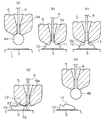
本発明の一実施の形態に係るワイヤボンディング方法を図1及び図2により説明する。図2(b)は本発明の一実施の形態に係るワイヤボンディング方法を用いてダイと配線間にワイヤボンディングした状態の1例を示す。セラミック基板やプリント基板等の基板又はリードフレーム等よりなる回路基板1上には、パット2aが形成されたダイ2がマウントされている。また回路基板1には配線3が形成されている。配線3上にはバンプ10が形成されており、パット2aとバンプ10間にはワイヤ4が接続されている。5はワイヤ4が挿通されたキャピラリを示す。
【0013】
次に図2(b)に示すワイヤボンディングは次の工程によって行われる。まず、図1(a)に示すように、キャピラリ5の貫通孔5aに挿通されたワイヤ4の先端に図示しない電気トーチによりボール4aを形成する。次に図1(b)に示すように、キャピラリ5を下降させて配線3上にボールボンディングを行う。これにより、ボール4aの一部は貫通孔5a内に盛り上がり、バンプ10上にホール部分11が形成される。続いて図1(c)に示すように、キャピラリ5の下端のエッジ部5bがホール部分11の高さ以内に位置するようにキャピラリ5を上昇させる。
【0014】
次に図1(d)に示すように、キャピラリ5をパット2a側(図2(b)参照)と反対方向で斜め下方に移動させた後、キャピラリ5を上昇させてワイヤ4を切断する。これにより、バンプ10上にキャピラリ5のエッジ部5bによって傾斜面12が形成される。この傾斜面12の傾斜角度θは、キャピラリ5を斜め下方に移動させる傾斜角度によって自由に設定できる。またキャピラリ5のエッジ部5bでホール部分11を斜め下方に押すので、面積が大きくて平坦な傾斜面12が形成される。
【0015】
次に図1(e)に示すように、ワイヤ4の先端に電気トーチによりボール4bを形成させる。続いて図2(a)に示すように、キャピラリ5をダイ2のパット2a上に位置させ1次ボンディングを行う。次に図2(b)に示すように、ワイヤ4のルーピングを行い、ワイヤ4をバンプ10の傾斜面12の上部に位置させ、ワイヤ4を傾斜面12に2次ボンディングを行い、ワイヤ4を切断する。
【0016】
図3は本発明の一実施の形態に係るワイヤボンディング方法を用いてダイと配線間にワイヤボンディングした状態の他の例を示す。前記実施の形態においては、配線3上にバンプ10を形成し、パット2a上に1次ボンディングを行い、バンプ10上の傾斜面12に2次ボンディングを行った。図3の場合は、パット2a上に図1(a)乃至図1(e)の工程でバンプ10を形成し、バンプ10上の傾斜面12を配線3側の反対側に形成した。そして、図2(a)及び図2(b)の工程で配線3上に1次ボンディングを行い、バンプ10上の傾斜面12に2次ボンディングを行ってワイヤ4を切断した。即ち、図1及び図2の場合は、パット2aが第1導体となり、配線3が第2導体となる。図3の場合は、配線3が第1導体となり、パット2aが第2導体となる。
【0017】
【発明の効果】
本発明は、第1導体上に1次ボンディングを行った後、第2導体上に2次ボンディングを行い、前記第1導体と前記第2導体間をワイヤボンディングする方法において、前記第2導体上にボールボンディングを行いバンプを形成した後にキャピラリを上昇させ、この場合におけるキャピラリを上昇させる高さは、バンプ形成時に前記キャピラリの貫通孔に盛り上がったホール部分の高さ以内であり、続いてキャピラリを前記第1導体側と反対方向で斜め下方に移動させてバンプの上部に傾斜面を形成させ、その後前記1次ボンディングを行い、次に前記バンプに対して前記第1導体側からワイヤをルーピングして前記バンプ上部の傾斜面上に前記2次ボンディングを行うので、バンプ上に形成する傾斜面の傾斜角度を自由に設定できる。
【図面の簡単な説明】
【図1】本発明の一実施の形態に係るワイヤボンディング方法の工程を示す工程図である。
【図2】図1の続きの工程を示す工程図である。
【図3】本発明の一実施の形態に係るワイヤボンディング方法を用いてダイと配線間がワイヤボンディングされた状態の他の例を示す図である。
【符号の説明】
1 回路基板
2 ダイ
2a パット
3 配線
4 ワイヤ
4a、4b ボール
5 キャピラリ
5a 貫通孔
5b エッジ部
10 バンプ
11 ホール部分
12 傾斜面[0001]
BACKGROUND OF THE INVENTION
The present invention relates to a wire bonding method for wire bonding between two conductors.
[0002]
[Prior art]
As a wire bonding method for connecting a wire between the first conductor and the bump on the second conductor after the bump is formed on the second conductor, Patent Document 1 and
[0003]
[Patent Document 1]
Japanese Patent Laid-Open No. 10-112471 [Patent Document 2]
JP 2002-280410 A [0004]
In Patent Document 1, bump bonding is performed on a second conductor to form a bump, and the wedge bonding is performed at a position opposite to the first conductor with respect to the bump, and then primary bonding is performed on the first conductor. Subsequently, a wire is looped from the first conductor side to the bump, and secondary bonding is performed on the bump.
[0005]
In
[0006]
[Problems to be solved by the invention]
Patent Document 1 has a problem as described in [0006] in
[0007]
In
[0008]
However, in
[0009]
An object of the present invention is to provide a wire bonding method capable of freely setting an inclination angle of an inclined surface formed on a bump.
[0010]
[Means for Solving the Problems]
According to a first aspect of the present invention for solving the above-mentioned problem, after performing primary bonding on the first conductor, secondary bonding is performed on the second conductor, and the gap between the first conductor and the second conductor is performed. In the method of wire bonding , the capillary is raised after ball bonding is performed on the second conductor to form a bump . In this case, the height at which the capillary is raised is a hole raised in the through hole of the capillary at the time of bump formation. Next, the capillary is moved obliquely downward in the direction opposite to the first conductor side to form an inclined surface on the bump, and then the primary bonding is performed, and then the bump is applied to the bump. On the other hand, a wire is looped from the first conductor side, and the secondary bonding is performed on the inclined surface above the bump.
[0012]
DETAILED DESCRIPTION OF THE INVENTION
A wire bonding method according to an embodiment of the present invention will be described with reference to FIGS. FIG. 2B shows an example of a state where wire bonding is performed between the die and the wiring using the wire bonding method according to the embodiment of the present invention. A
[0013]
Next, wire bonding shown in FIG. 2B is performed by the following process. First, as shown in FIG. 1A, a
[0014]
Next, as shown in FIG. 1D, after the capillary 5 is moved obliquely downward in the direction opposite to the
[0015]
Next, as shown in FIG.1 (e), the ball |
[0016]
FIG. 3 shows another example of a state in which wire bonding is performed between a die and wiring using the wire bonding method according to the embodiment of the present invention. In the embodiment, the
[0017]
【The invention's effect】
The present invention relates to a method for performing secondary bonding on a second conductor after performing primary bonding on the first conductor, and wire bonding between the first conductor and the second conductor. After forming the bump by ball bonding to the capillary , the capillary is raised . In this case, the height for raising the capillary is within the height of the hole raised in the through hole of the capillary at the time of bump formation. Is moved obliquely downward in the opposite direction to the first conductor side to form an inclined surface on the upper part of the bump, and then the primary bonding is performed, and then the wire is looped from the first conductor side to the bump. And since the said secondary bonding is performed on the inclined surface of the said bump upper part, the inclination angle of the inclined surface formed on a bump can be set freely.
[Brief description of the drawings]
FIG. 1 is a process diagram showing processes of a wire bonding method according to an embodiment of the present invention.
FIG. 2 is a process diagram illustrating a process continued from FIG. 1;
FIG. 3 is a diagram showing another example of a state where a die and a wiring are wire-bonded using the wire bonding method according to the embodiment of the present invention.
[Explanation of symbols]
DESCRIPTION OF SYMBOLS 1
Claims (1)
Priority Applications (3)
| Application Number | Priority Date | Filing Date | Title |
|---|---|---|---|
| JP2003038313A JP3854233B2 (en) | 2003-02-17 | 2003-02-17 | Wire bonding method |
| TW092135142A TW200416911A (en) | 2003-02-17 | 2003-12-12 | Wire bonding method |
| KR1020040000473A KR100577586B1 (en) | 2003-02-17 | 2004-01-06 | Wire bonding method |
Applications Claiming Priority (1)
| Application Number | Priority Date | Filing Date | Title |
|---|---|---|---|
| JP2003038313A JP3854233B2 (en) | 2003-02-17 | 2003-02-17 | Wire bonding method |
Publications (2)
| Publication Number | Publication Date |
|---|---|
| JP2004247673A JP2004247673A (en) | 2004-09-02 |
| JP3854233B2 true JP3854233B2 (en) | 2006-12-06 |
Family
ID=33022872
Family Applications (1)
| Application Number | Title | Priority Date | Filing Date |
|---|---|---|---|
| JP2003038313A Expired - Lifetime JP3854233B2 (en) | 2003-02-17 | 2003-02-17 | Wire bonding method |
Country Status (3)
| Country | Link |
|---|---|
| JP (1) | JP3854233B2 (en) |
| KR (1) | KR100577586B1 (en) |
| TW (1) | TW200416911A (en) |
Families Citing this family (1)
| Publication number | Priority date | Publication date | Assignee | Title |
|---|---|---|---|---|
| JP4625858B2 (en) * | 2008-09-10 | 2011-02-02 | 株式会社カイジョー | Wire bonding method, wire bonding apparatus, and wire bonding control program |
-
2003
- 2003-02-17 JP JP2003038313A patent/JP3854233B2/en not_active Expired - Lifetime
- 2003-12-12 TW TW092135142A patent/TW200416911A/en unknown
-
2004
- 2004-01-06 KR KR1020040000473A patent/KR100577586B1/en active IP Right Grant
Also Published As
| Publication number | Publication date |
|---|---|
| KR100577586B1 (en) | 2006-05-08 |
| KR20040074913A (en) | 2004-08-26 |
| JP2004247673A (en) | 2004-09-02 |
| TW200416911A (en) | 2004-09-01 |
| TWI302721B (en) | 2008-11-01 |
Similar Documents
| Publication | Publication Date | Title |
|---|---|---|
| JP3913134B2 (en) | Bump forming method and bump | |
| JP3854232B2 (en) | Bump forming method and wire bonding method | |
| JP4298665B2 (en) | Wire bonding method | |
| US7453156B2 (en) | Wire bond interconnection | |
| US20070029367A1 (en) | Semiconductor device | |
| JP4106039B2 (en) | Wire bonding method | |
| US7025247B2 (en) | Wire bonding method | |
| JP4021378B2 (en) | Wire bonding method | |
| JP3854233B2 (en) | Wire bonding method | |
| JP2002280410A (en) | Wire-bonding method | |
| JP2004179303A (en) | Element package and its manufacturing method | |
| JP2007012642A (en) | Wire bonding method | |
| JP4879923B2 (en) | Semiconductor device | |
| JP2006196597A (en) | Electronic apparatus and manufacturing method thereof | |
| JP5048990B2 (en) | Semiconductor device and manufacturing method thereof | |
| JP2004221264A (en) | Semiconductor device and its manufacturing method | |
| JPH0744018Y2 (en) | Projection electrode structure | |
| JP4313958B2 (en) | Wire bonding method | |
| JP3855523B2 (en) | Connection method between IC chip and circuit board | |
| JPH0982742A (en) | Wire bonding method | |
| JP4547405B2 (en) | Wire bonding method | |
| JPH10294397A (en) | Flip chip mounting board | |
| JP2006054383A (en) | Wire bonding method | |
| JP2000323514A (en) | Method for connecting between ic chip and circuit board | |
| JP2004273904A (en) | Semiconductor device and wire bonding method |
Legal Events
| Date | Code | Title | Description |
|---|---|---|---|
| A621 | Written request for application examination |
Free format text: JAPANESE INTERMEDIATE CODE: A621 Effective date: 20050331 |
|
| A977 | Report on retrieval |
Free format text: JAPANESE INTERMEDIATE CODE: A971007 Effective date: 20060607 |
|
| A131 | Notification of reasons for refusal |
Free format text: JAPANESE INTERMEDIATE CODE: A131 Effective date: 20060613 |
|
| A521 | Request for written amendment filed |
Free format text: JAPANESE INTERMEDIATE CODE: A523 Effective date: 20060724 |
|
| TRDD | Decision of grant or rejection written | ||
| A01 | Written decision to grant a patent or to grant a registration (utility model) |
Free format text: JAPANESE INTERMEDIATE CODE: A01 Effective date: 20060825 |
|
| A61 | First payment of annual fees (during grant procedure) |
Free format text: JAPANESE INTERMEDIATE CODE: A61 Effective date: 20060907 |
|
| R150 | Certificate of patent or registration of utility model |
Ref document number: 3854233 Country of ref document: JP Free format text: JAPANESE INTERMEDIATE CODE: R150 Free format text: JAPANESE INTERMEDIATE CODE: R150 |
|
| FPAY | Renewal fee payment (event date is renewal date of database) |
Free format text: PAYMENT UNTIL: 20100915 Year of fee payment: 4 |
|
| R250 | Receipt of annual fees |
Free format text: JAPANESE INTERMEDIATE CODE: R250 |
|
| FPAY | Renewal fee payment (event date is renewal date of database) |
Free format text: PAYMENT UNTIL: 20100915 Year of fee payment: 4 |
|
| FPAY | Renewal fee payment (event date is renewal date of database) |
Free format text: PAYMENT UNTIL: 20110915 Year of fee payment: 5 |
|
| R250 | Receipt of annual fees |
Free format text: JAPANESE INTERMEDIATE CODE: R250 |
|
| FPAY | Renewal fee payment (event date is renewal date of database) |
Free format text: PAYMENT UNTIL: 20110915 Year of fee payment: 5 |
|
| FPAY | Renewal fee payment (event date is renewal date of database) |
Free format text: PAYMENT UNTIL: 20120915 Year of fee payment: 6 |
|
| R250 | Receipt of annual fees |
Free format text: JAPANESE INTERMEDIATE CODE: R250 |
|
| FPAY | Renewal fee payment (event date is renewal date of database) |
Free format text: PAYMENT UNTIL: 20120915 Year of fee payment: 6 |
|
| FPAY | Renewal fee payment (event date is renewal date of database) |
Free format text: PAYMENT UNTIL: 20130915 Year of fee payment: 7 |
|
| EXPY | Cancellation because of completion of term |