JP3839733B2 - Imaging apparatus and image data output method - Google Patents
Imaging apparatus and image data output method Download PDFInfo
- Publication number
- JP3839733B2 JP3839733B2 JP2002039914A JP2002039914A JP3839733B2 JP 3839733 B2 JP3839733 B2 JP 3839733B2 JP 2002039914 A JP2002039914 A JP 2002039914A JP 2002039914 A JP2002039914 A JP 2002039914A JP 3839733 B2 JP3839733 B2 JP 3839733B2
- Authority
- JP
- Japan
- Prior art keywords
- image data
- pixel
- camera
- defect
- pattern
- Prior art date
- Legal status (The legal status is an assumption and is not a legal conclusion. Google has not performed a legal analysis and makes no representation as to the accuracy of the status listed.)
- Expired - Fee Related
Links
Images


Classifications
-
- H—ELECTRICITY
- H04—ELECTRIC COMMUNICATION TECHNIQUE
- H04N—PICTORIAL COMMUNICATION, e.g. TELEVISION
- H04N25/00—Circuitry of solid-state image sensors [SSIS]; Control thereof
- H04N25/60—Noise processing, e.g. detecting, correcting, reducing or removing noise
- H04N25/68—Noise processing, e.g. detecting, correcting, reducing or removing noise applied to defects
Landscapes
- Engineering & Computer Science (AREA)
- Multimedia (AREA)
- Signal Processing (AREA)
- Transforming Light Signals Into Electric Signals (AREA)
- Solid State Image Pick-Up Elements (AREA)
- Facsimile Image Signal Circuits (AREA)
Description
【0001】
【発明の属する技術分野】
本発明は、CCDイメージセンサ,CMOSイメージセンサなどの固定撮像素子を備える撮像装置および画像データ出力方法に関する。
【0002】
【従来の技術】
デジタルスチルカメラ,デジタルビデオカメラなどの撮像装置は、CCDイメージセンサなどの固体撮像素子を備えている。このような固体撮像素子の中には、その製造時に、受光量に応じた電荷を生成することができない画素や,暗電流の不均一によるノイズが規定値以上に発生してしまう画素などのいわゆる欠陥画素が形成される場合がある。
【0003】
欠陥画素は、その画像信号を表示させた際に、黒傷,白傷などの傷となって撮像画像に現れ、画像品質を著しく低下させる。そのため、固体撮像素子の製造時においては、その検査過程で、欠陥画素であるか否かを判断する。欠陥画素であると判断された場合は、その欠陥画素の位置(座標)などを表わす「欠陥画素データ」を、撮像装置の記憶部(メモリ)に予め記憶していた。
【0004】
そして、撮像装置は画像欠陥補正装置を備え、この画像欠陥補正装置は上記「欠陥画素データ」に基づいて欠陥画素に対する欠陥補正を行っていた。この画像欠陥補正装置に関する技術としては、特開平1−105671号公報に記載のものがある。
【0005】
即ち、上述した画像欠陥補正装置は、実際の撮像時において、予め記憶してした「欠陥画素データ」に対応する欠陥画素のみを、この欠陥画素の周辺画素データに基づき補正処理していた。欠陥画素を補正する方法としてメモリに予め記憶した「欠陥画素データ」のみを用いるのは、連写,動画などの実際の撮影処理を速くするためである。このような欠陥画素補正方法は、小型軽量で低価格のデジタルスチルカメラにおいて、要請されるものである。
【0006】
そして、上記デジタルスチルカメラでは、「欠陥画素データ」を記憶するメモリの上限値(限界)が、コストなどによって予め決められていた。上記メモリの個数は、256個乃至1000個の範囲内に抑えられていた。そのため、上記メモリの範囲内における欠陥画素は、その周辺画素データに基づき、適切に補正され、良好な画像を得ていた。
【0007】
また、従来のデジタルスチルカメラの中には、画像データの画像を第三者に見られないようにするため、画像データ自体を暗号化する暗号処理手段を有するものがあった。この暗号処理に関する技術としては、特開2000−165720号公報に記載のものがある。
【0008】
【発明が解決しようとする課題】
ところで、不特定多数のユーザに貸し出し回収する、いわゆる使い捨てタイプのデジタルスチルカメラなどを販売する販売システムが、構築されることを仮に想定すると、上記デジタルスチルカメラを借りた第三者が、そのCCDイメージセンサ,CMOSイメージセンサなどの撮像素子を他の撮像装置に利用(流用)することが考えられる。なお、上述した画像データ自体を暗号する場合には、撮像装置における処理などに負荷が生じる。
【0009】
本発明の目的は、上記事実を考慮して、撮像素子の流用を阻止し得る撮像装置および画像データ出力方法を提供することにある。
【0010】
【課題を解決するための手段】
請求項1記載の撮像装置では、欠陥補正ができる限界以上の個数の欠陥画素を、予め定めた配列パターンに応じて形成した撮像素子を備える。請求項1記載に係る発明において、予め定めた配列パターンに応じて形成した欠陥画素を、欠陥補正できるメモリなどの限界以上の個数としたので、上記欠陥画素の配列パターンに対応するパターンデータが認識できない場合には上記撮像素子によって撮像された画像データを正常に再生させることができない。
【0011】
一方、上記欠陥画素の配列パターンに対応するパターンデータを認識し得る場合には、既知のパターンデータに基づき、予め形成した欠陥画素を適切に補正し、良好な画像データを得る。即ち、請求項1記載に係る発明によれば、撮像素子に欠陥補正ができる限界以上の個数の欠陥画素を、予め定めた配列パターンに応じて形成したので、CCDイメージセンサ,CMOSイメージセンサなどの撮像素子の流用を阻止できる。なお、請求項1記載に係る発明は、撮像素子の流用を阻止し得るように構成したので、不特定多数のユーザに貸し出し回収する、使い捨てタイプのデジタルカメラなどの撮像装置に適している。
【0012】
また、請求項1記載に係る発明では、撮像素子(ハード)自体に欠陥補正ができる限界以上の個数の欠陥画素を、予め定めた配列パターンに応じて形成することにより、撮像された画像データを正常に再生できないようにしたので、画像データ自体を暗号する場合と異なり、撮像装置における処理などに負荷が全く生じない。
【0013】
請求項2記載に係る発明では、請求項1に係る撮像装置において、G画素を前記欠陥画素とすることを特徴とする。請求項2記載に係る発明によれば、欠陥画素を、撮像素子において画素数の多いG画素としたので、S/N(信号対雑音比)の劣化を最小限にできる。
【0014】
請求項3記載の画像データ出力方法では、欠陥補正ができる限界以上の個数の欠陥画素を予め定めた配列パターンに応じて形成した撮像素子によって撮像された画像データを読出すと共に、前記欠陥画素の配列パターンに対応するパターンデータを読出し、前記パターンデータに基づき、前記画像データを補正し出力する。
【0015】
欠陥補正ができる限界以上の個数の欠陥画素を予め定めた配列パターンに応じて形成した撮像素子によって撮像された画像データを、撮像装置における例えばフラッシュROMなどの記録媒体から読出す。上記欠陥画素の配列パターンは予め異なる複数種類が存在し、そのため上記画像データに記録された欠陥画素の配列パターンに対応するパターンデータを読出す。そして、読出したパターンデータに基づき、画像データを補正すると共に、例えばプリンタなどに出力する。
【0016】
請求項3記載に係る発明によれば、予め定めた配列パターンに応じて形成した欠陥画素を、欠陥補正できるメモリなどの限界以上の個数としたので、上記欠陥画素の配列パターンに対応するパターンデータが認識できない場合には上記撮像素子によって撮像された画像データを正常に再生させることができない。すなわち、請求項3記載に係る発明によれば、撮像素子に欠陥補正ができる限界以上の個数の欠陥画素を、予め定めた配列パターンに応じて形成したので、撮像素子の流用を阻止できる。
【0017】
なお、本発明では、画像データを記録する記録媒体を、スマート・メディア(SmartMedia(R))、コンパクト・フラッシュ(CompactFlash)、ATA(AT Attachment)カード、フロッピィディスク、CD−R(Compact Disc-Recordable)、CD−RW(Compact Disc-ReWritable)などとしても良い。また、本発明に係る撮像装置は、デジタルスチルカメラ,デジタルビデオカメラ,撮像機能を備えた携帯電話,パーソナル・コンピュータ,PDA(Personal Digital Assistance)などを含む概念である。
【0018】
【発明の実施の形態】
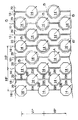
以下、図1乃至図6に基づいて、本発明の実施形態であるデジタルスチルカメラ(以下、単に「カメラ」という)について説明する。なお、図1は本実施形態のカメラにおけるCCDイメージセンサの要部を示す平面図、図2は図1に示すCCDイメージセンサとは異なるタイプの要部を示す平面図である。
【0019】
ここで、本実施形態のカメラは、不特定多数のユーザに貸し出し回収する、いわゆる使い捨てタイプである。また、本実施形態では、小型軽量で低価格なカメラとしたので、「欠陥画素データ」を記憶するメモリの個数(限界)が、256個となっている。
【0020】
カメラに内蔵された撮像素子であるCCDイメージセンサは、図1に示すように、半導体基板(図示省略)上に、平面形状が正八角形のフォトダイオード(光電変換素子である画素)14を所定間隔(垂直画素ピッチVP)で垂直方向に複数配列した第1の光電変換素子列16と、複数のフォトダイオード14を第1の光電変換素子列16と同じ間隔で垂直方向に配列し、かつ第1の光電変換素子列16に対して垂直方向に垂直画素ピッチVPに対して1/2ずらして配置された第2の光電変換素子列18と、で構成された素子列の組を水平方向に複数組並べて構成されている。
【0021】
そして、隣り合う第1の光電変換素子列16及び隣り合う第2の光電変換素子列18は、垂直画素ピッチと同じ間隔(水平画素ピッチHP)で配置され、第1の光電変換素子列16に含まれるフォトダイオード14により構成される光電変換素子行に対して、第2の光電変換素子列18に含まれるフォトダイオード14により構成される光電変換素子行は、水平方向に水平画素ピッチHPに対して1/2ずらして配置されている。即ち、フォトダイオード14は、いわゆるハニカム状に配列されている。
【0022】
なお、相互に接近して配列された第1の光電変換素子列16と第2の光電変換素子列18との間には、フォトダイオード14で発生した信号電荷を読み出して垂直方向に転送する垂直電荷転送チャネル20が各々設けられている。垂直電荷転送チャネル20は、両側に位置する光電変換素子列の各フォトダイオード間に侵入した侵入部20Aと非侵入部20Bとが交互に位置するように連続して構成され、ハニカム状に配列したフォトダイオード14の間を蛇行しながら垂直方向に延びている。
【0023】
また、図1の想像線に示すように、所定位置のフォトダイオード14は、故意に欠陥を設けたフォトダイオード(以下、単に「故意欠陥画素」という)15としている。この故意欠陥画素15は、黒を検出するための領域(オプティカルブラック部分)を形成する工程において、フォトダイオード14の表面部分をアルミニウムで覆い隠す(マスクする)ことによって形成する。
【0024】
即ち、本実施形態では、故意欠陥画素15を予め定めた配列パターンに応じて形成すると共に、故意欠陥画素15の個数をカメラのメモリ(「欠陥画素データ」を記憶するメモリ)で欠陥補正ができる限界(256個)以上の個数としている。故意欠陥画素15は欠陥補正できるメモリの限界に対する数値として例えば1000個以上を形成し、かつ故意欠陥画素15の配列パターンは規則正しくなっている。
【0025】
なお、本実施形態においても、CCDイメージセンサの製造時に不慮に形成された欠陥画素に対し、その欠陥画素の位置(座標)などを表わす「欠陥画素データ」がカメラの記憶部(メモリ)に予め記憶されている。そして、本実施形態においても、実際の撮像時において、予め記憶していた上記「欠陥画素データ」に対応する欠陥画素を、この周辺画素データに基づいて補正処理する。
【0026】
上述のように構成されたCCDイメージセンサは、被写界に向けて配置された撮像レンズによって結像される被写体像を電気信号に変換する。CCDイメージセンサの撮像面には、GストライプR/B完全市松配列のRGB原色フィルタが被着されている。即ち、R(レッド),G(グリーン),およびB(ブルー)の各フィルタに対応する画素(フォトダイオード)14において、G画素は、R画素またはB画素の2倍の画素数となっている。
【0027】
そして、本実施形態では、R・Bの画素よりも画素数の多いG画素を、上述した故意欠陥画素15の主対象としている。そのため、本実施形態においては、故意欠陥画素15を、画素数の多いG画素としたので、S/N(信号対雑音比)の劣化を最小限にし得る。
【0028】
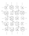
図2には、図1とは平面形状および配列が異なる画素を備えたCCDイメージセンサが示されている。即ち、図2に示すように、平面形状が正四角形のフォトダイオード(画素)22は、図示しない半導体基板上に、垂直方向および平行方向において所定間隔をもって整列している。
【0029】
また、図2の想像線に示すように、所定位置のフォトダイオード22は、故意に欠陥を設けたフォトダイオード(以下、単に「故意欠陥画素」という)23としている。この故意欠陥画素23は、オプティカルブラック(OB)部分を形成する工程において、フォトダイオード22の表面部分をアルミニウムでマスクすることによって形成する。その他の構成は図1に示すCCDイメージセンサと同様であるので、説明は省略する。
【0030】
なお、カメラには、CCDイメージセンサからの出力信号に基づき被写体像を示すデジタル画像データを生成すると共にCCDイメージセンサなどを駆動するためのタイミング信号を生成する信号処理部と、主としてCCDイメージセンサによる撮像によって得られたデジタル画像データを記憶するSDRAM(Synchronous Dynamic RAM)と、カメラの全体的な動作を司る制御部(CPU)と、を含んで構成されている。
【0031】
また、CPUは、図示しない所定容量のラインバッファを内蔵した撮像制御部と、所定の圧縮形式(本実施形態ではJPEG(Joint Photographic Experts Group)形式)でデジタル画像データに対して圧縮処理を施すと共に、圧縮処理されたデジタル画像データに対して伸張処理を施す圧縮・伸張部と、がバスを介して相互に接続されて構成されている。
【0032】
さらに、カメラは、CCDイメージセンサによる撮像によって得られた被写体像や各種情報を表示する表示部(LCD)と、電源スイッチなどの各種操作キーを備える操作部と、カメラのID(このIDは故意欠陥画素15,23の配列パターンを特定するための「カメラID」である)や各種パラメータなどを記憶した記憶部(フラッシュROM)と、USBコネクタなどのインターフェイス32(図3参照)を接続する外部接続部と、を含んで構成されている。
【0033】
即ち、上記配列パターンは複数種類が存在し、カメラ(撮像素子)毎に異なるよう設定されている。また、フラッシュROMは、装置本体に内蔵され、取外し不可能となっている。
【0034】
外部接続部は、CPUに接続されており、I/F32を介して接続された外部端末(図3に示すような再生装置30など)との間の通信を司る。なお、信号処理部は、相関2重サンプリング回路(CDS)と、ゲインコントローラと、A/Dコンバータと、タイミングジェネレータと、を含んで構成されている。
【0035】
そして、信号処理部は、RGB原色フィルタのフィルタ配列に対応するCCDイメージセンサの各画素を3つの原色RGBとして表わす画素補間機能を有し、R,G,およびB各原色の画素から1つのRGB画素を補間処理によって生成する機能を有している。即ち、CCDイメージセンサから出力された信号は、相関2重サンプリング回路によって相関2重サンプリング処理が施され、ゲインコントローラによってCCDイメージセンサにおけるR(赤),G(緑),B(青)毎の感度調整が施された後、各画素毎のR、G、B信号としてA/Dコンバータに加えられる。
【0036】
A/Dコンバータは、ゲインコントローラから順次加えられるR,G,B信号を、各々12ビットのR,G,B信号(以下、「デジタル画像データ」という。)に変換してCPUに出力する。そして、CPUは、内蔵しているラインバッファにA/Dコンバータから順次入力されるデジタル画像データを、蓄積して一旦SDRAMに格納する。
【0037】
SDRAMに格納されたデジタル画像データは、CPUによって読み出され、これらに光源種に応じたデジタルゲインをかけることでホワイトバランス調整を行なうと共に、ガンマ処理及びシャープネス処理を行なって8ビットのデジタル画像データを生成し、更にYC信号処理して輝度信号Yとクロマ信号Cr、Cb(以下、単に「YC信号」という。)を生成し、YC信号を再びSDRAMに格納する。
【0038】
シャッターボタンが撮影者によって押圧操作された場合には、SDRAMに格納されたYC信号を、圧縮・伸張部によって所定の圧縮形式で圧縮した後にフラッシュROMに記憶する。即ち、フラッシュROMには、被写体の画像データが記憶される。また、図3に示すように、I/F32には再生装置30が接続され、そしてフラッシュROMに記憶されているデジタル画像データ,カメラIDなどの各種情報は再生装置30に読込まれる。
【0039】
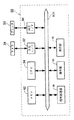
次に、図3に基づき、再生装置30の構成を説明する。なお、本実施形態の再生装置30は、いわゆるラボ(写真現像店)に設置されたパーソナル・コンピュータ(パソコン)である。
【0040】
再生装置30には、その装置全体の動作を司るCPU(中央演算処理装置)34と,カメラ28などが接続される入力用のI/F32と,I/F32から入力されたデジタル画像データを処理する信号処理部36と,テンキーなど配置された操作部38と,デジタル画像データなどを表示する表示部40と,欠陥画素の配列パターンに対応する欠陥パターンデータおよびカメラIDなどの各種情報が記憶されたメモリ42と,信号処理部36で画像処理などされたデジタル画像データを外部に出力する出力用のI/F44と,がバスBUSを介して相互に接続されて構成されている。なお、再生装置30であるパソコンは一般的なものであるので、その詳細な説明は省略する。
【0041】
図4に示すように、メモリ42の記憶領域45は、カメラIDと欠陥パターンとを対応付けるデータ(図5参照)を予め記憶したテーブル領域46,カメラ28からのデジタル画像データなどを記憶する画像領域47,欠陥パターンに基づいてデジタル画像データを欠陥補正するプログラムなどが予め記憶されたプログラム領域48,テーブル領域46の欠陥パターンに対応する欠陥パターンデータ(故意欠陥画素の座標などのデータ)が予め記憶された欠陥パターンデータ領域49などを備えている。
【0042】
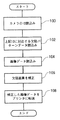
引続き、図6に基づき、図3に示す再生装置30におけるデジタル画像データの出力処理について説明する。なお、図6に示す処理は使い捨てタイプのカメラを販売する販売システムが構築されることが前提であり、そして撮像済みのカメラ28をラボに持ち込む。また、本処理は、I/F32にカメラ28を接続し、かつI/F44にプリンタ50を接続していることが前提である。
【0043】
図6に示すように、ステップ100ではカメラ28のフラッシュROMに記憶されているカメラIDを読込み、ステップ102では読込んだカメラIDに対応する欠陥パターンデータを図3に示すメモリ42の欠陥パターンデータ領域49(図4参照)から読込む。即ち、欠陥パターンデータは、カメラIDと欠陥パターンとが対応付けられたテーブル(図5参照)に基づき、欠陥パターンデータ領域49から読出す。
【0044】
また、ステップ104ではカメラ28のフラッシュROMから出力されたデジタル画像データを画像領域47(図4参照)から読込み、ステップ106では欠陥パターンデータに基づいて故意欠陥画素15(図1参照)または23(図2参照)を補正する。即ち、上記「欠陥パターンデータ」に対応する欠陥画素を、この周辺画素データに基づいて補正処理する。
【0045】
そして、ステップ108では、補正処理されたデジタル画像データを、図3に示すプリンタ50に転送する。プリンタ50は、信号処理部36で画像処理されたデジタル画像データに基づく画像を、プリントアウトする。即ち、本実施形態においては、故意欠陥画素15,23の配列パターンに対応する既知の欠陥パターンデータに基づき、予め形成した故意欠陥画素15,23を適切に補正し、良好な画像データを得ることができる。
【0046】
なお、上述したように、本実施形態に係るカメラ28は使い捨てタイプであるので、プリントアウト後に、業者がカメラ28を回収する。また、本処理の終了後は、カメラ28のフラッシュROMに記録されたデジタル画像データを、全て消去し、その後の再利用を図る。
【0047】
本実施形態においては、予め定めた配列パターンに応じて形成した故意欠陥画素15,23を、欠陥補正できるメモリなどの限界以上の個数としたので、故意欠陥画素15,23の配列パターンに対応する欠陥パターンデータが認識できない(読出すことができない)場合すなわち欠陥パターンデータを記憶している再生装置30以外ではデジタル画像データを正常に再生させることができない。
【0048】
従って、本実施形態によれば、CCDイメージセンサに欠陥補正ができる限界以上の個数の故意欠陥画素15,23を、予め定めた配列パターンに応じて形成したので、カメラ28に配置されたCCDイメージセンサを他の撮像装置に利用(流用)することができない。なお、上述したように、本実施形態のCCDイメージセンサは、その流用を阻止し得るように構成したので、使い捨てタイプのデジタルカメラに適している。
【0049】
また、本実施形態では、CCDイメージセンサ(ハード)自体に欠陥補正ができる限界以上の個数の故意欠陥画素15,23を予め定めた配列パターンに応じて形成することにより、撮像された画像データを正常に再生できないようにしたので、画像データ自体を暗号する場合と異なり、カメラ28における処理などに負荷が全く生じない。
【0050】
なお、上記各実施形態では撮像素子をCCDイメージセンサとした例であるが、本発明に係る撮像素子はCMOSイメージセンサなどとしても良い。また、故意欠陥画素15,23の形成は、物理的手段であるアルミニウム等でマスクする他に、転送電極を部分的に欠損させたり,所定位置に配置するべきフォトダイオード(画素)を設けない(開口させる)ようにしても良い。さらに、本発明に係る欠陥画素の形成は、上述した遮光の他に、白傷などが形成できるように開光させても良い。
【0051】
本発明では、欠陥パターンデータ(故意欠陥画素15,23の座標データなど)を、暗号化させても良い。この場合には、画像データのセキュリティが確保される。また、本実施形態ではカメラ28をI/F32に接続した例であるが、本発明はこれに限定されるものではなく、例えばカメラに対して着脱可能なスマート・メディアなどを再生装置30に装着できるようにしても良い。
【0052】
本実施形態ではプリンタ50をI/F44に接続しプリントアウトする例であるが、上記「欠陥パターンデータ」に基づいて補正処理されたデジタル画像データをCD−R,スマート・メディア,コンパクト・フラッシュ,ATAカード,フロッピィディスク,CD−RWなどの記録媒体に記録させるようにしても良い。また、本実施形態において説明したプログラムの処理の流れ(図6参照)は一例であり、本発明の主旨を逸脱しない範囲内において適宜変更可能であることは言うまでもない。
【0053】
【発明の効果】
以上説明したように、本発明によれば、予め定めた配列パターンに応じて形成した欠陥画素を、欠陥補正できるメモリなどの限界以上の個数としたので、上記欠陥画素の配列パターンに対応するパターンデータが認識できない場合には上記撮像素子によって撮像された画像データを正常に再生させることができない。即ち、本発明によれば、撮像素子に欠陥補正ができる限界以上の個数の欠陥画素を、予め定めた配列パターンに応じて形成したので、撮像素子の流用を阻止できる。
【図面の簡単な説明】
【図1】本発明の実施形態に係るCCDイメージセンサの要部を示す平面図である。
【図2】図1に示すCCDイメージセンサとは異なるタイプの要部を示す平面図である。
【図3】本実施形態に係る再生装置の構成を示すブロック図である。
【図4】図3に示すメモリのメモリマップを示す図である。
【図5】図4に示すテーブル領域のメモリマップを示す図である。
【図6】本実施形態に係る再生装置におけるデジタル画像データの出力処理の流れを示すフローチャートである。
【符号の説明】
14、22 フォトダイオード(画素)
15、23 故意欠陥画素
28 デジタルカメラ(撮像装置)[0001]
BACKGROUND OF THE INVENTION
The present invention relates to an image pickup apparatus including a fixed image pickup device such as a CCD image sensor or a CMOS image sensor, and an image data output method.
[0002]
[Prior art]
Imaging devices such as digital still cameras and digital video cameras include solid-state imaging devices such as CCD image sensors. Among such solid-state image sensors, so-called pixels that cannot generate charges according to the amount of received light or pixels that generate noise exceeding a specified value due to non-uniform dark current at the time of manufacture. A defective pixel may be formed.
[0003]
When the image signal is displayed, the defective pixel appears as a flaw such as a black flaw or a white flaw in the captured image, and the image quality is significantly reduced. Therefore, at the time of manufacturing the solid-state imaging device, it is determined whether or not it is a defective pixel in the inspection process. If it is determined that the pixel is a defective pixel, “defective pixel data” indicating the position (coordinates) of the defective pixel is stored in advance in a storage unit (memory) of the imaging apparatus.
[0004]
The imaging device includes an image defect correction device, and the image defect correction device performs defect correction on the defective pixel based on the “defective pixel data”. A technique related to this image defect correction apparatus is disclosed in Japanese Patent Laid-Open No. 1-105671.
[0005]
That is, the above-described image defect correction apparatus corrects only defective pixels corresponding to “defective pixel data” stored in advance based on the peripheral pixel data of the defective pixels at the time of actual imaging. The reason for using only “defective pixel data” stored in the memory in advance as a method for correcting defective pixels is to speed up actual photographing processing such as continuous shooting and moving images. Such a defective pixel correction method is required for a small, light and low-cost digital still camera.
[0006]
In the digital still camera, the upper limit value (limit) of the memory for storing “defective pixel data” is determined in advance according to the cost. The number of the memories is limited to the range of 256 to 1000. For this reason, defective pixels within the memory range are appropriately corrected based on the peripheral pixel data to obtain a good image.
[0007]
Also, some conventional digital still cameras have encryption processing means for encrypting the image data itself so that an image of the image data cannot be viewed by a third party. As a technique related to this encryption processing, there is one described in Japanese Patent Laid-Open No. 2000-165720.
[0008]
[Problems to be solved by the invention]
By the way, if it is assumed that a sales system that sells and collects so-called disposable digital still cameras that are lent out and collected to an unspecified number of users is constructed, a third party who borrows the digital still camera will have its CCD. It is conceivable to use (appropriate) an image sensor such as an image sensor or a CMOS image sensor for another imaging device. Note that when the above-described image data itself is encrypted, there is a load on processing in the imaging apparatus.
[0009]
An object of the present invention is to provide an imaging apparatus and an image data output method that can prevent the diversion of an imaging element in consideration of the above fact.
[0010]
[Means for Solving the Problems]
According to another aspect of the present invention, there is provided an imaging device in which a defective pixel having a number exceeding a limit capable of correcting a defect is formed in accordance with a predetermined arrangement pattern. In the invention according to
[0011]
On the other hand, when the pattern data corresponding to the arrangement pattern of the defective pixels can be recognized, the defective pixels formed in advance are appropriately corrected based on the known pattern data to obtain good image data. In other words, according to the first aspect of the present invention, since the defective pixels of the image sensor more than the limit capable of correcting the defect are formed in accordance with the predetermined arrangement pattern, the CCD image sensor, the CMOS image sensor, etc. Diversion of the image sensor can be prevented. Since the invention according to
[0012]
According to the first aspect of the present invention, the imaged image data is obtained by forming a defective pixel having a number larger than a limit capable of defect correction in the image pickup device (hardware) itself according to a predetermined arrangement pattern. Since normal reproduction is not possible, unlike the case where the image data itself is encrypted, there is no load on the processing in the imaging apparatus.
[0013]
According to a second aspect of the present invention, in the imaging device according to the first aspect, a G pixel is the defective pixel. According to the second aspect of the present invention, since the defective pixel is a G pixel having a large number of pixels in the image sensor, the deterioration of S / N (signal to noise ratio) can be minimized.
[0014]
According to another aspect of the image data output method of the present invention, the image data picked up by the image pickup device formed according to a predetermined array pattern is read out from a defect pixel having a number exceeding the limit capable of correcting the defect. Pattern data corresponding to the array pattern is read, and the image data is corrected and output based on the pattern data.
[0015]
Image data captured by an imaging device in which a defect pixel exceeding the limit capable of defect correction is formed according to a predetermined array pattern is read from a recording medium such as a flash ROM in the imaging apparatus. There are a plurality of different types of defective pixel array patterns in advance, and therefore pattern data corresponding to the defective pixel array pattern recorded in the image data is read. Then, based on the read pattern data, the image data is corrected and output to a printer, for example.
[0016]
According to the third aspect of the present invention, the number of defective pixels formed in accordance with the predetermined array pattern is set to a number exceeding the limit of a memory or the like that can correct the defect, so that the pattern data corresponding to the array pattern of the defective pixels Cannot be recognized, the image data picked up by the image pickup device cannot be reproduced normally. That is, according to the third aspect of the invention, the number of defective pixels exceeding the limit capable of correcting the defect in the image sensor is formed in accordance with the predetermined arrangement pattern, so that diversion of the image sensor can be prevented.
[0017]
In the present invention, recording media for recording image data are smart media (SmartMedia®), compact flash (CompactFlash), ATA (AT Attachment) card, floppy disk, CD-R (Compact Disc-Recordable). CD-RW (Compact Disc-ReWritable) or the like. The imaging apparatus according to the present invention is a concept including a digital still camera, a digital video camera, a mobile phone having an imaging function, a personal computer, a PDA (Personal Digital Assistance), and the like.
[0018]
DETAILED DESCRIPTION OF THE INVENTION
Hereinafter, a digital still camera (hereinafter simply referred to as “camera”) according to an embodiment of the present invention will be described with reference to FIGS. 1 to 6. FIG. 1 is a plan view showing the main part of the CCD image sensor in the camera of this embodiment, and FIG. 2 is a plan view showing the main part of a type different from the CCD image sensor shown in FIG.
[0019]
Here, the camera of the present embodiment is a so-called disposable type that is lent out and collected to an unspecified number of users. In this embodiment, since the camera is small and light and inexpensive, the number (limit) of memories storing “defective pixel data” is 256.
[0020]
As shown in FIG. 1, a CCD image sensor, which is an image sensor incorporated in a camera, has a regular octagonal photodiode (pixel which is a photoelectric conversion element) 14 on a semiconductor substrate (not shown) at a predetermined interval. A plurality of first photoelectric conversion element rows 16 arranged in the vertical direction at (vertical pixel pitch VP) and a plurality of
[0021]
The adjacent first photoelectric conversion element array 16 and the adjacent second photoelectric
[0022]
Note that, between the first photoelectric conversion element array 16 and the second photoelectric
[0023]
Further, as indicated by an imaginary line in FIG. 1, the
[0024]
That is, in the present embodiment, the intentionally
[0025]
Also in the present embodiment, “defective pixel data” indicating the position (coordinates) of the defective pixel, which is formed inadvertently at the time of manufacturing the CCD image sensor, is stored in advance in the storage unit (memory) of the camera. It is remembered. Also in the present embodiment, at the time of actual imaging, a defective pixel corresponding to the “defective pixel data” stored in advance is corrected based on the peripheral pixel data.
[0026]
The CCD image sensor configured as described above converts a subject image formed by an imaging lens arranged toward the object field into an electrical signal. An RGB primary color filter having a G-strip R / B complete checkered arrangement is attached to the imaging surface of the CCD image sensor. That is, in the pixel (photodiode) 14 corresponding to the R (red), G (green), and B (blue) filters, the G pixel has twice the number of pixels as the R pixel or the B pixel. .
[0027]
In this embodiment, the G pixel having a larger number of pixels than the R / B pixels is set as the main target of the intentional
[0028]
FIG. 2 shows a CCD image sensor provided with pixels having a different planar shape and arrangement from FIG. That is, as shown in FIG. 2, the photodiodes (pixels) 22 having a regular tetragonal planar shape are aligned on the semiconductor substrate (not shown) with a predetermined interval in the vertical direction and the parallel direction.
[0029]
Further, as indicated by an imaginary line in FIG. 2, the
[0030]
The camera includes a signal processing unit that generates digital image data indicating a subject image based on an output signal from the CCD image sensor and generates a timing signal for driving the CCD image sensor and the like, and a CCD image sensor. It includes an SDRAM (Synchronous Dynamic RAM) that stores digital image data obtained by imaging, and a control unit (CPU) that controls the overall operation of the camera.
[0031]
In addition, the CPU performs compression processing on the digital image data in a predetermined compression format (in this embodiment, JPEG (Joint Photographic Experts Group) format) and an imaging control unit having a predetermined capacity line buffer (not shown). A compression / decompression unit that performs decompression processing on the compressed digital image data is connected to each other via a bus.
[0032]
The camera further includes a display unit (LCD) for displaying a subject image and various information obtained by imaging by a CCD image sensor, an operation unit having various operation keys such as a power switch, and a camera ID (this ID is intentionally An external that connects a storage unit (flash ROM) storing various parameters and the like to an interface 32 (see FIG. 3) such as a USB connector, which is a “camera ID” for specifying an array pattern of
[0033]
That is, there are a plurality of types of array patterns, which are set to be different for each camera (imaging device). The flash ROM is built in the main body of the apparatus and cannot be removed.
[0034]
The external connection unit is connected to the CPU and manages communication with an external terminal (such as the
[0035]
The signal processing unit has a pixel interpolation function that represents each pixel of the CCD image sensor corresponding to the filter arrangement of the RGB primary color filter as three primary colors RGB, and outputs one RGB from the R, G, and B primary colors. It has a function of generating pixels by interpolation processing. That is, the signal output from the CCD image sensor is subjected to correlated double sampling processing by the correlated double sampling circuit, and the gain controller controls each of R (red), G (green) and B (blue) in the CCD image sensor. After the sensitivity adjustment, the R / G / B signals for each pixel are added to the A / D converter.
[0036]
The A / D converter converts R, G, and B signals sequentially added from the gain controller into 12-bit R, G, and B signals (hereinafter referred to as “digital image data”) and outputs the signals to the CPU. Then, the CPU accumulates digital image data sequentially input from the A / D converter in the built-in line buffer and temporarily stores it in the SDRAM.
[0037]
The digital image data stored in the SDRAM is read out by the CPU, white balance adjustment is performed by applying a digital gain corresponding to the light source type to these, and gamma processing and sharpness processing are performed to obtain 8-bit digital image data. Are further processed to generate a luminance signal Y and chroma signals Cr and Cb (hereinafter simply referred to as “YC signal”), and the YC signal is stored again in the SDRAM.
[0038]
When the shutter button is pressed by the photographer, the YC signal stored in the SDRAM is compressed in a predetermined compression format by the compression / expansion unit and then stored in the flash ROM. In other words, the image data of the subject is stored in the flash ROM. As shown in FIG. 3, a
[0039]
Next, based on FIG. 3, the structure of the reproducing | regenerating
[0040]
The
[0041]
As shown in FIG. 4, the
[0042]
The digital image data output process in the
[0043]
As shown in FIG. 6, in
[0044]
In
[0045]
In
[0046]
As described above, since the
[0047]
In the present embodiment, the intentional
[0048]
Therefore, according to the present embodiment, since the CCD image sensor has the number of intentional
[0049]
In the present embodiment, the CCD image sensor (hardware) itself forms a larger number of intentionally
[0050]
In each of the above embodiments, the image sensor is a CCD image sensor. However, the image sensor according to the present invention may be a CMOS image sensor or the like. In addition, the intentionally
[0051]
In the present invention, defect pattern data (such as the coordinate data of the intentionally
[0052]
In this embodiment, the
[0053]
【The invention's effect】
As described above, according to the present invention, the number of defective pixels formed in accordance with a predetermined array pattern is set to a number that exceeds a limit of a memory that can perform defect correction. When the data cannot be recognized, the image data picked up by the image pickup device cannot be normally reproduced. That is, according to the present invention, since the number of defective pixels exceeding the limit that can correct the defect in the image sensor is formed in accordance with the predetermined arrangement pattern, diversion of the image sensor can be prevented.
[Brief description of the drawings]
FIG. 1 is a plan view showing a main part of a CCD image sensor according to an embodiment of the present invention.
FIG. 2 is a plan view showing a main part of a type different from the CCD image sensor shown in FIG.
FIG. 3 is a block diagram showing a configuration of a playback apparatus according to the present embodiment.
4 is a diagram showing a memory map of the memory shown in FIG. 3. FIG.
FIG. 5 is a diagram showing a memory map of the table area shown in FIG. 4;
FIG. 6 is a flowchart showing a flow of output processing of digital image data in the reproducing apparatus according to the embodiment.
[Explanation of symbols]
14, 22 Photodiode (pixel)
15, 23 Intentionally
Claims (3)
前記欠陥画素の配列パターンに対応するパターンデータを読出し、
前記パターンデータに基づき、前記画像データを補正し出力する画像データ出力方法。While reading out the image data imaged by the imaging device formed in accordance with a predetermined array pattern of a defective pixel more than the limit capable of defect correction,
Read pattern data corresponding to the defective pixel array pattern,
An image data output method for correcting and outputting the image data based on the pattern data.
Priority Applications (2)
| Application Number | Priority Date | Filing Date | Title |
|---|---|---|---|
| JP2002039914A JP3839733B2 (en) | 2002-02-18 | 2002-02-18 | Imaging apparatus and image data output method |
| US10/367,797 US7271833B2 (en) | 2002-02-18 | 2003-02-19 | Image pickup apparatus, image data processing apparatus, image data outputting method, image data processing system and image pickup device |
Applications Claiming Priority (1)
| Application Number | Priority Date | Filing Date | Title |
|---|---|---|---|
| JP2002039914A JP3839733B2 (en) | 2002-02-18 | 2002-02-18 | Imaging apparatus and image data output method |
Publications (2)
| Publication Number | Publication Date |
|---|---|
| JP2003244552A JP2003244552A (en) | 2003-08-29 |
| JP3839733B2 true JP3839733B2 (en) | 2006-11-01 |
Family
ID=27780800
Family Applications (1)
| Application Number | Title | Priority Date | Filing Date |
|---|---|---|---|
| JP2002039914A Expired - Fee Related JP3839733B2 (en) | 2002-02-18 | 2002-02-18 | Imaging apparatus and image data output method |
Country Status (2)
| Country | Link |
|---|---|
| US (1) | US7271833B2 (en) |
| JP (1) | JP3839733B2 (en) |
Families Citing this family (9)
| Publication number | Priority date | Publication date | Assignee | Title |
|---|---|---|---|---|
| US7369167B2 (en) * | 2003-06-02 | 2008-05-06 | Micron Technology, Inc. | Photo diode ID for CMOS imagers |
| GB0506566D0 (en) * | 2005-03-31 | 2005-05-04 | E2V Tech Uk Ltd | Method of identifying a photoelectric sensor array |
| JP2007184905A (en) * | 2005-12-07 | 2007-07-19 | Pentax Corp | Image signal processing apparatus and image signal processing method |
| US7787034B2 (en) * | 2006-04-27 | 2010-08-31 | Avago Technologies General Ip (Singapore) Pte. Ltd. | Identification of integrated circuits using pixel or memory cell characteristics |
| JP4662966B2 (en) * | 2007-07-19 | 2011-03-30 | 富士フイルム株式会社 | Imaging device |
| US20110199512A1 (en) * | 2010-02-18 | 2011-08-18 | Win-How Chen | Single Use Digital Camera |
| US9224030B2 (en) | 2014-01-10 | 2015-12-29 | Qualcomm Incorporated | Sensor identification |
| CN106851135B (en) * | 2016-09-09 | 2019-07-09 | 安霸公司 | The method and apparatus being replaced for determining sensor |
| US11626442B2 (en) * | 2020-08-10 | 2023-04-11 | Taiwan Semiconductor Manufacturing Company, Ltd. | Methods for forming image sensors |
Family Cites Families (8)
| Publication number | Priority date | Publication date | Assignee | Title |
|---|---|---|---|---|
| JP2565263B2 (en) | 1987-10-17 | 1996-12-18 | ソニー株式会社 | Image defect correction device for solid-state imaging device |
| WO1993014602A1 (en) * | 1992-01-08 | 1993-07-22 | Ikegami Tsushinki Co., Ltd. | Solid-state imaging device and solid-state imaging element used therefor |
| WO1998024186A2 (en) * | 1996-11-12 | 1998-06-04 | California Institute Of Technology | Semiconductor imaging sensor with on-chip encryption |
| US7324133B2 (en) * | 1998-11-06 | 2008-01-29 | Fotomedia Technologies, Llc | Method and apparatus for controlled camera useability |
| JP2000165720A (en) | 1998-11-26 | 2000-06-16 | Konica Corp | Image formation system and digital still camera and printing device |
| JP3337067B2 (en) * | 1999-05-07 | 2002-10-21 | 日本電気株式会社 | Manufacturing method of cylindrical capacitor lower electrode |
| WO2003024094A1 (en) * | 2001-09-10 | 2003-03-20 | Nikon Corporation | Digital camera system, image storage apparatus, and digital camera |
| JP4018456B2 (en) * | 2002-06-03 | 2007-12-05 | 富士フイルム株式会社 | Imaging device |
-
2002
- 2002-02-18 JP JP2002039914A patent/JP3839733B2/en not_active Expired - Fee Related
-
2003
- 2003-02-19 US US10/367,797 patent/US7271833B2/en not_active Expired - Fee Related
Also Published As
| Publication number | Publication date |
|---|---|
| US20040160520A1 (en) | 2004-08-19 |
| JP2003244552A (en) | 2003-08-29 |
| US7271833B2 (en) | 2007-09-18 |
Similar Documents
| Publication | Publication Date | Title |
|---|---|---|
| JP5026951B2 (en) | Imaging device driving device, imaging device driving method, imaging device, and imaging device | |
| JP4253634B2 (en) | Digital camera | |
| JP2003032694A (en) | Solid-state image sensor and digital camera | |
| US8111298B2 (en) | Imaging circuit and image pickup device | |
| JP4129338B2 (en) | Color imaging device and imaging apparatus | |
| JP3839733B2 (en) | Imaging apparatus and image data output method | |
| JP5033711B2 (en) | Imaging device and driving method of imaging device | |
| US6034724A (en) | Imaging device utilizing a line-crawling correction coefficient | |
| JP4817529B2 (en) | Imaging apparatus and image processing method | |
| CN101827226A (en) | Camera device and control method thereof | |
| JP2005198319A (en) | Image sensor and method | |
| JP2001016598A (en) | Color imaging device and imaging device | |
| JP4581633B2 (en) | Color signal correction method, apparatus and program | |
| JP2000106678A (en) | Image pickup device | |
| JP2005109993A (en) | Imaging device | |
| JP2001203969A (en) | Image pickup device and its operation control method | |
| JPH1169226A (en) | Electronic camera | |
| JP3925914B2 (en) | Pixel defect correction apparatus and pixel defect correction method | |
| JP4284282B2 (en) | Imaging apparatus and solid-state imaging device | |
| JP2009118430A (en) | Imaging device, driving method of the imaging device, image generation device, and image generation method | |
| JPH11266468A (en) | Test pattern generator for picture display device | |
| JP4105556B2 (en) | Digital camera and recorded image data recording method | |
| JP2007235877A (en) | Multi-plate type solid-state imaging device module and imaging apparatus | |
| JP2009302653A (en) | Image pickup device | |
| JP2004297614A (en) | Imaging apparatus and display method in imaging apparatus |
Legal Events
| Date | Code | Title | Description |
|---|---|---|---|
| A621 | Written request for application examination |
Free format text: JAPANESE INTERMEDIATE CODE: A621 Effective date: 20040315 |
|
| TRDD | Decision of grant or rejection written | ||
| A01 | Written decision to grant a patent or to grant a registration (utility model) |
Free format text: JAPANESE INTERMEDIATE CODE: A01 Effective date: 20060801 |
|
| A61 | First payment of annual fees (during grant procedure) |
Free format text: JAPANESE INTERMEDIATE CODE: A61 Effective date: 20060803 |
|
| R150 | Certificate of patent or registration of utility model |
Free format text: JAPANESE INTERMEDIATE CODE: R150 |
|
| FPAY | Renewal fee payment (event date is renewal date of database) |
Free format text: PAYMENT UNTIL: 20090811 Year of fee payment: 3 |
|
| S111 | Request for change of ownership or part of ownership |
Free format text: JAPANESE INTERMEDIATE CODE: R313111 |
|
| FPAY | Renewal fee payment (event date is renewal date of database) |
Free format text: PAYMENT UNTIL: 20090811 Year of fee payment: 3 |
|
| R350 | Written notification of registration of transfer |
Free format text: JAPANESE INTERMEDIATE CODE: R350 |
|
| FPAY | Renewal fee payment (event date is renewal date of database) |
Free format text: PAYMENT UNTIL: 20090811 Year of fee payment: 3 |
|
| FPAY | Renewal fee payment (event date is renewal date of database) |
Free format text: PAYMENT UNTIL: 20100811 Year of fee payment: 4 |
|
| FPAY | Renewal fee payment (event date is renewal date of database) |
Free format text: PAYMENT UNTIL: 20110811 Year of fee payment: 5 |
|
| FPAY | Renewal fee payment (event date is renewal date of database) |
Free format text: PAYMENT UNTIL: 20110811 Year of fee payment: 5 |
|
| FPAY | Renewal fee payment (event date is renewal date of database) |
Free format text: PAYMENT UNTIL: 20120811 Year of fee payment: 6 |
|
| FPAY | Renewal fee payment (event date is renewal date of database) |
Free format text: PAYMENT UNTIL: 20120811 Year of fee payment: 6 |
|
| FPAY | Renewal fee payment (event date is renewal date of database) |
Free format text: PAYMENT UNTIL: 20130811 Year of fee payment: 7 |
|
| R250 | Receipt of annual fees |
Free format text: JAPANESE INTERMEDIATE CODE: R250 |
|
| R250 | Receipt of annual fees |
Free format text: JAPANESE INTERMEDIATE CODE: R250 |
|
| LAPS | Cancellation because of no payment of annual fees |