JP3833859B2 - Semiconductor device and manufacturing method thereof - Google Patents
Semiconductor device and manufacturing method thereof Download PDFInfo
- Publication number
- JP3833859B2 JP3833859B2 JP29270399A JP29270399A JP3833859B2 JP 3833859 B2 JP3833859 B2 JP 3833859B2 JP 29270399 A JP29270399 A JP 29270399A JP 29270399 A JP29270399 A JP 29270399A JP 3833859 B2 JP3833859 B2 JP 3833859B2
- Authority
- JP
- Japan
- Prior art keywords
- substrate
- semiconductor chip
- semiconductor
- protruding electrode
- semiconductor device
- Prior art date
- Legal status (The legal status is an assumption and is not a legal conclusion. Google has not performed a legal analysis and makes no representation as to the accuracy of the status listed.)
- Expired - Lifetime
Links
Images


Classifications
-
- H—ELECTRICITY
- H01—ELECTRIC ELEMENTS
- H01L—SEMICONDUCTOR DEVICES NOT COVERED BY CLASS H10
- H01L24/00—Arrangements for connecting or disconnecting semiconductor or solid-state bodies; Methods or apparatus related thereto
- H01L24/93—Batch processes
- H01L24/95—Batch processes at chip-level, i.e. with connecting carried out on a plurality of singulated devices, i.e. on diced chips
- H01L24/97—Batch processes at chip-level, i.e. with connecting carried out on a plurality of singulated devices, i.e. on diced chips the devices being connected to a common substrate, e.g. interposer, said common substrate being separable into individual assemblies after connecting
-
- H—ELECTRICITY
- H01—ELECTRIC ELEMENTS
- H01L—SEMICONDUCTOR DEVICES NOT COVERED BY CLASS H10
- H01L2224/00—Indexing scheme for arrangements for connecting or disconnecting semiconductor or solid-state bodies and methods related thereto as covered by H01L24/00
- H01L2224/01—Means for bonding being attached to, or being formed on, the surface to be connected, e.g. chip-to-package, die-attach, "first-level" interconnects; Manufacturing methods related thereto
- H01L2224/10—Bump connectors; Manufacturing methods related thereto
- H01L2224/15—Structure, shape, material or disposition of the bump connectors after the connecting process
- H01L2224/16—Structure, shape, material or disposition of the bump connectors after the connecting process of an individual bump connector
- H01L2224/161—Disposition
- H01L2224/16151—Disposition the bump connector connecting between a semiconductor or solid-state body and an item not being a semiconductor or solid-state body, e.g. chip-to-substrate, chip-to-passive
- H01L2224/16221—Disposition the bump connector connecting between a semiconductor or solid-state body and an item not being a semiconductor or solid-state body, e.g. chip-to-substrate, chip-to-passive the body and the item being stacked
- H01L2224/16225—Disposition the bump connector connecting between a semiconductor or solid-state body and an item not being a semiconductor or solid-state body, e.g. chip-to-substrate, chip-to-passive the body and the item being stacked the item being non-metallic, e.g. insulating substrate with or without metallisation
Description
【0001】
【発明の属する技術分野】
この発明は、三次元実装に有利な半導体装置およびその製造方法に関する。
【0002】
【従来の技術】
半導体パッケージの薄型化とその三次元実装とにより、半導体装置の設置スペースの削減を図ることが提案されている。
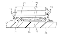
図9には、このような目的のために提案されている半導体装置70の構成例を示す断面図である。この半導体装置70は、テープ状基板71の打ち抜き部に薄い半導体チップ72を配置して、その活性表面側(図9の上面側)保護樹脂73で封止して構成されている。半導体チップ72には、シングルポイントボンディングによりインナーリード74が接続されていて、外部の実装基板80との接続は、基板71上でインナーリード74に接続されたアウターリード75によって行うようになっている。この半導体装置70の三次元実装は、アウターリード75をそれぞれ実装基板80に接続することによって行われる。
【0003】
【発明が解決しようとする課題】
しかし、このような構成では、三次元実装の際に、各半導体装置70のアウターリード75を個別に実装基板80に接続する必要があるから、三次元実装の工程が複雑で、かつ、困難である。
また、アウターリード75を外方に引き出す構成であるので、半導体装置70全体の専有面積が比較的大きいという問題もある。
【0004】
そこで、この発明の目的は、上述の技術的課題を解決し、三次元実装に有利な半導体装置およびその製造方法を提供することである。
【0005】
【課題を解決するための手段および発明の効果】
上記の目的を達成するための請求項1記載の発明は、基板と、この基板の表面に活性表面を対向させたフェースダウン状態で接合された半導体チップと、前記基板の前記半導体チップが接合された表面から突出させて設けられた突起電極と、この突起電極の頭部が露出する状態で、この突起電極および前記半導体チップを封止する保護樹脂とを含み、前記基板には、この基板の裏面側から前記突起電極の基部への電気接続を可能とするための貫通孔が形成されており、前記保護樹脂、前記突起電極の頭部および前記半導体チップの非活性表面が面一をなしていることを特徴とする半導体装置である。
【0006】
前記突起電極は、半導体チップの周囲(可及的に半導体チップの近傍)に設けられていることが好ましい。
また、前記基板は、テープ状基板等の薄型の基板であることが好ましい。
請求項1の発明によれば、半導体チップと、外部接続用の電極としての突起電極とが基板の同じ側の表面に設けられている。また、前記基板の裏面側から前記突起電極の基部への電気接続を可能とするための貫通孔が形成されている。この貫通孔を介して、三次元的に積層された複数の半導体装置相互間の接続を容易に図ることができる。
【0007】
しかも、突起電極を用いていることにより、半導体装置の占有面積を少なくすることができるうえ、三次元実装された半導体装置間の配線長も短くできる。
なお、前記貫通孔は、突起電極の直下の位置に形成されることが好ましい。
請求項2記載の発明は、基板の表面に活性表面を対向させたフェースダウン状態で、半導体チップを前記基板に接合するチップ接合工程と、前記基板の表面に、この表面から突出した突起電極を形成する電極形成工程と、前記半導体チップおよび突起電極を、前記突起電極の頭部を露出させた状態で保護樹脂により封止する樹脂封止工程と、前記基板に、この基板の裏面側から前記突起電極の基部への電気接続を可能とするための貫通孔を形成する工程とを含むことを特徴とする半導体装置の製造方法である。
【0008】
この方法により、請求項1に記載された半導体装置を作製することができる。前記貫通孔は、突起電極の基部の直下に形成することが好ましい。
請求項3記載の発明は、前記チップ接合工程では、複数の半導体チップが前記基板に接合され、前記電極形成工程では、前記複数の半導体チップに対応した複数の突起電極が形成され、前記製造方法は、さらに、前記基板を予め定める切断ラインに沿って切断することにより、半導体装置の個片を切り出す切り出し工程を含むことを特徴とする請求項2記載の半導体装置の製造方法である。
【0009】
この方法により、複数個の半導体装置を一括して生産することができる。
なお、この場合に、樹脂封止工程は、複数の半導体チップおよび複数の突起電極を一括して封止するようにして行われることが好ましい。複数の半導体チップを封止する保護樹脂は、一体化されていてもよいし、個別の半導体チップごとに分かれていてもよい。複数の半導体チップを封止する保護樹脂が一体化されている場合には、切り出し工程では、保護樹脂および基板が同時に切断されることが好ましい。したがって、切り出し工程は、樹脂封止工程の後に行われることが好ましい。
【0010】
なお、樹脂封止工程は、突起電極および半導体チップを保護樹脂で封止する工程と、突起電極の頭部を露出させるために保護樹脂の表層部を除去する工程とを含んでいてもよい。
また、前記製造方法には、半導体チップの非活性表面を研磨または研削して半導体チップを薄型化する工程がさらに含まれていることが好ましい。この工程では、保護樹脂が同時に研磨または研削されて、装置全体の薄型化が図られてもよい。
【0012】
【発明の実施の形態】
以下では、この発明の実施の形態を、添付図面を参照して詳細に説明する。
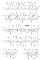
図1は、この発明の一実施形態に係る半導体装置の構成を示す斜視図である。この半導体装置10は、ポリイミド基板やガラスエボキシ基板などのテープ状の基板1の表面に、半導体チップCを、その表面(活性表面)を対向させたフェースダウン状態で接合した構造を有している。この実施形態においては、半導体チップCは、平面視において矩形形状に成形されていて、半導体チップCの周囲の領域には、基板1の表面から突出した外部接続電極としての突起電極(この実施形態では柱状の電極)Tが複数個形成されている。
【0013】
基板1の表面において半導体チップCまたは突起電極Tが形成されていない領域は、保護樹脂(たとえばエポキシ樹脂など)5で樹脂封止されており、半導体装置10全体を補強しているとともに、突起電極Tの変形を防止する役割などをに担っている。半導体チップCの表面は、基板1に対向しており、かつ、その側面が保護樹脂5で封止されていることにより、外部から保護されている。
【0014】
この実施形態では、保護樹脂5、突起電極Tの頭部および半導体チップCの非活性表面Cbは、面一をなしている。
図2は、上記の半導体装置の組立工程を工程順に示す断面図である。図2(a)は、半導体チップ接合工程を示す。ポリイミド基板などの基板1には、予め配線パターンが、たとえば銅の電解めっきなどによって形成されている。この配線パターン上には、複数の突起電極Tが形成される(電極形成工程)。この突起電極Tが形成された基板1の表面1aには、複数の半導体チップCがフェースダウンで接合される。すなわち、半導体チップCは、トランジスタや抵抗などの素子が形成された活性表層領域側の表面である活性表面Caを基板1に対向させた状態で、その表面に形成されたバンプBを介して、基板1に接合され、この基板1に形成された配線パターンに電気的に接続される。これにより、半導体チップCは、基板1上の配線パターンを介して突起電極Tと電気的に接続されることになる。
【0015】
基板1に接合される半導体チップCは、比較的大きな厚み、たとえば、300〜700μm程度の厚みを有している。このような半導体チップCは、300〜700μmの厚い半導体ウエハ(図示せず)をダイシングソーで分割することによって得られる。このように十分に厚いウエハは、ダイシング工程において割れや欠けが生じることがなく、かつ、このダイシング工程を経て得られる厚い半導体チップCは、その後に基板1に接合するためのハンドリング時においても割れや欠けが生じるおそれがない。
【0016】
半導体チップCが基板1に接合された後には、必要に応じて、活性表面Caと基板1との間の空隙に液状樹脂(アンダーフィル)が注入される。
図2(b)は、半導体チップ接合工程に続いて行われる樹脂封止工程を示す。この樹脂封止工程では、基板1に接合された複数個の半導体チップCおよびその周囲に配置された複数の突起電極Tを一括して収容するキャビティが形成された金型(図示せず)が用いられ、基板1上の複数個の半導体チップCおよび突起電極Tが保護樹脂5によって一括して封止される(樹脂封止工程)。これにより、各半導体チップCの側壁12と、活性表面Caとは反対側の非活性表面Cbとが保護樹脂5で覆われ、突起電極Tはその全体が保護樹脂5中に埋没する。また、活性表面Caと基板1との間の空隙の側方が、保護樹脂5で封止され、こうして活性表面Caが保護される。
【0017】
なお、この樹脂封止工程では、突起電極Tの頭部および/または半導体チップCの裏面(非活性表面)Cbが保護樹脂5から露出するようにされてもよい。
図2(c)は、樹脂封止工程に続いて、保護樹脂5の硬化後に行われる研削工程を示す。研削工程では、研削目標厚Toまで、グラインダーを用いて研削が行われる。すなわち、保護樹脂5が研削され、半導体チップCの非活性表面Cbが露出させられる。その後は、保護樹脂5および半導体チップCの非活性表面Cb側の研削が同時に進行し、研削目標厚Toまで研削される。この研削目標厚Toは、たとえば、研削後の半導体チップCの厚みtが、100〜200μm程度となるように設定される。
【0018】
続いて、図2(d)に示すように、たとえば、ダイシングソー15を用いて、半導体チップC同士の間に設定された切断ラインDに沿って、保護樹脂5および基板1が切断され、図2(e)に示すように、半導体装置10の個片が切り出される。この切り出し工程によって切り出された半導体装置10は、半導体チップCの側壁が全周にわたって保護樹脂5で覆われている。そして、この保護樹脂5の上面5aと研削後の非活性表面Cbとは面一になっており、半導体チップCの角部は保護樹脂5により覆われていて、いずれの位置においても保護されている。
【0019】
こうして切り出された半導体装置10の個片には、必要に応じて、図2(e)に示すように、突起電極Tの基部の直下において、基板1に貫通孔7が形成される。この貫通孔7は、基板1の裏側から、貫通孔7を介して突起電極Tへの電気接続を図るためのものである。
そこで、さらに、必要に応じて、図2(f)に示すように、貫通孔7には、たとえば、半田ボール8が印刷により転写されて形成される。この半田ボール8は、必要に応じてリフローを施すことにより、図3に示すように、貫通孔7を通って、基板1の表面1a側に形成された配線パターン13に接続される。この配線パターン13には、半導体チップCがバンプBを介して接続されており、かつ、別の位置で突起電極Tが接合されている。
【0020】
図4は、上述のような半導体装置10の三次元実装を説明するための斜視図である。実装基板50の表面には、銅などによる印刷配線51が形成されており、半導体装置10の実装領域52が設定されている。この実装領域52上に、複数の半導体装置10が積み重ねられて実装される。ただし、複数の半導体装置10は、同じ種類の半導体チップCを内蔵したものであってもよく、また、異なる種類の半導体チップCを内蔵したものであってもよい。
【0021】
各層の半導体装置10の相互間の接続は、各層の半導体装置10の突起電極T同士が、基板1の貫通孔7(図2および図3参照)を介して接続されることにより達成されている。そして、各層の半導体装置10の実装基板50上の回路への電気接続は、最下層(実装基板50の最も近い層)の半導体装置10の突起電極Tが、実装基板50の表面の印刷配線51に貫通孔7を介して接続されることにより達成される。各層の半導体装置10間の接合および最下層の半導体装置10の印刷配線51に対する接合は、半田ボール8をリフローにより溶融させることにより達成される。
【0022】
以上のようにこの実施形態によれば、基板1の同じ表面側に半導体チップCおよび突起電極Tを設け、これらを樹脂封止することにより、薄型の半導体パッケージを実現している。したがって、パッケージの外方にリードを引き出す必要がないので、実装基板50上での占有面積が少なくなる。また、半導体装置10の三次元実装は、基板1に貫通孔7を設けることによって達成されており、上述の従来技術のように、各層の半導体装置のリードを個別に実装基板に接合する必要がない。したがって、半導体装置10の三次元実装を極めて簡単に行うことができる。
【0023】
また、突起電極Tは、その周囲が保護樹脂5(絶縁物)に包囲されているので、リーク電流などが生じることがなく電気的に安定であり、かつ、変形や破損のおそれがなく機械的にも安定である。
さらには、突起電極Tを用いていることにより、上下の半導体装置10の各半導体チップCの間の配線距離が短く、電気的動作を高速化することができるという利点もある。
【0024】
なお、上下に積層される複数の半導体装置10のうち、いずれか1つの特定の半導体装置10の特定の突起電極Tのみを独立して実装基板50に接続したい場合には、図5に示す構成を採用すればよい。すなわち、当該特定の半導体装置10よりも下層の半導体装置10の基板1には、当該特定の突起電極Tに対応する位置に、独立した(すなわち、当該下層の半導体装置10の半導体チップCとは電気的に接続されていない)中継用の突起電極Tcを設ける。これにより、この中継用の突起電極Tcを介して、上記特定の半導体装置の特定の突起電極Tを、他の半導体装置10とは独立した状態で、実装基板50に接続することができる。
【0025】
以上、この発明の一実施形態について説明したが、この発明は、他の形態で実施することもできる。
たとえば、上述の実施形態では、同じ大きさの半導体チップCを有する複数の半導体装置10を積層して三次元実装する例を説明したが、図6に示すように、異なる大きさの半導体チップCを内蔵した複数の半導体装置100についても、突起電極Tの配置を合わせておくことによって、上述の実施形態の場合と同様な三次元実装が可能である。
【0026】
また、上述の実施形態では、半導体チップCを上方に向けたフェースアップ状態で半導体装置10,100を実装基板50上に実装する例について説明したが、半導体チップCを実装基板50に対向させたフェースダウン状態で半導体装置10,100の実装を行ってもよい。
さらに、上述の実施形態では、基板1の貫通孔7に半田ボール8を設けるようにしているが、半田ボール8を設ける代わりに、貫通孔7にクリーム半田を配置し、リフロー法により、実装基板50または他の層の半導体装置10との接続を行うようにしてもよい。
【0027】
図7および図8は、参考例の構成を示す断面図である。上述の実施形態では、保護樹脂5、突起電極Tおよび半導体チップCの非活性表面Cbが面一になるようにしているが、図7の参考例では、突起電極Tの頭部が保護樹脂5の表面から突出しており、図8の参考例では、保護樹脂5の表面から半導体チップCの非活性表面Cb側が突出している。図7または図8の構造は、たとえば、保護樹脂5を十分に薄く形成することにより作製可能である。この場合に、突起電極Tの頭部に保護樹脂5が付着するおそれがあれば、グラインダーなどによる研磨または研削やエッチングによって、突起電極Tの頭部に付着した保護樹脂を除去すればよい。
【0028】
また、上記の実施形態では、基板1上に1つの半導体チップCが接合されて1つの半導体装置10,100が構成される例について説明したが、基板1上に2つ以上の半導体チップCを共通に接合し、2つ以上の半導体チップCを内蔵した半導体装置を構成してもよい。
さらに、上述の実施形態では、突起電極Tは、柱状のものとしたが、バンプ形状のものであっても構わない。
【0029】
また、上述の実施形態においては、製造工程において、複数の半導体チップCを一括して樹脂封止することとしているが、個々の半導体チップCまたは2〜3個ずつ(すなわち、所定の複数個)の半導体チップCごとに、樹脂封止を行ってもよい。
さらに、上述の各実施形態では、研削工程では、グラインダーによる機械的研削が行われることとしたが、この研削工程は、エッチング液を用いた化学的研削工程であってもよく、また、CMP(化学的機械的研磨)法のような化学的機械的研磨工程であってもよい。ただし、半導体チップの非活性表面側の研削または研磨は、研削精度よりも研削速度の方が重視されるから、上述の3つの方法のなかでは、グラインダーによる機械的研削方法が、生産効率の向上の観点からは、もっとも好ましい。
【0030】
グラインダーによる機械的研削が行われた樹脂および半導体チップの非活性表面は、連続した削り跡を有することになろうが、この削り跡は、必要に応じて、エッチングなどの化学的方法によって消すことができる。
また、上述の実施形態では、半導体装置の個片を切り出すための切り出し工程に、ダイシングソーを用いることとしたが、たとえば、レーザビームによる切断などの他の切断手法が採用されてもよい。
【0031】
その他、特許請求の範囲に記載された事項の範囲で種々の設計変更を施すことが可能である。
【図面の簡単な説明】
【図1】この発明の一実施形態に係る半導体装置の構成を示す斜視図である。
【図2】上記半導体装置の製造方法を工程順に示す断面図である。
【図3】突起電極の近傍の構成を拡大して示す断面図である。
【図4】上記半導体装置の三次元実装を説明するための斜視図である。
【図5】特定の半導体装置の特定の突起電極を他の半導体装置から独立して実装基板に接続するための構成を示す斜視図である。
【図6】異なるサイズの半導体チップを内蔵した半導体装置の三次元実装例を示す断面図である。
【図7】参考例に係る半導体装置の構成を示す断面図である。
【図8】他の参考例に係る半導体装置の構成を示す断面図である。
【図9】先行技術による薄型半導体装置の三次元実装例を示す断面図である。
【符号の説明】
1 基板
5 保護樹脂
10 半導体装置
50 実装基板
100 半導体装置
B バンプ
C 半導体チップ
Ca 活性表面
Cb 非活性表面
To 研削目標厚
T 突起電極
Tc 中継用の突起電極[0001]
BACKGROUND OF THE INVENTION
The present invention relates to a semiconductor device advantageous for three-dimensional mounting and a manufacturing method thereof.
[0002]
[Prior art]
It has been proposed to reduce the installation space of the semiconductor device by thinning the semiconductor package and its three-dimensional mounting.
FIG. 9 is a cross-sectional view showing a configuration example of a
[0003]
[Problems to be solved by the invention]
However, in such a configuration, it is necessary to individually connect the
Further, since the
[0004]
SUMMARY OF THE INVENTION An object of the present invention is to solve the above technical problem and provide a semiconductor device advantageous for three-dimensional mounting and a method for manufacturing the same.
[0005]
[Means for Solving the Problems and Effects of the Invention]
In order to achieve the above object, according to the first aspect of the present invention, a substrate, a semiconductor chip bonded in a face-down state with an active surface facing the surface of the substrate, and the semiconductor chip of the substrate are bonded. a protruding electrode formed to protrude from the surface, with the head of the protruding electrode is exposed, see contains a protective resin for sealing the protruding electrodes and the semiconductor chip, the substrate, the substrate A through hole is formed to allow electrical connection from the back surface side of the protruding electrode to the base of the protruding electrode, and the protective resin, the head of the protruding electrode, and the inactive surface of the semiconductor chip are flush with each other. It is a semiconductor device characterized by the above.
[0006]
The protruding electrode is preferably provided around the semiconductor chip (possibly near the semiconductor chip).
The substrate is preferably a thin substrate such as a tape substrate.
According to the first aspect of the present invention, the semiconductor chip and the protruding electrode as the external connection electrode are provided on the same surface of the substrate. In addition, a through hole is formed to enable electrical connection from the back side of the substrate to the base of the protruding electrode . Through this through-hole, it is possible to easily connect a plurality of semiconductor devices stacked three-dimensionally.
[0007]
In addition, by using the protruding electrode, the area occupied by the semiconductor device can be reduced, and the wiring length between the semiconductor devices mounted three-dimensionally can be shortened.
The through hole is preferably formed at a position directly below the protruding electrode.
According to a second aspect of the present invention, there is provided a chip bonding step of bonding a semiconductor chip to the substrate in a face-down state in which an active surface faces the surface of the substrate, and a protruding electrode protruding from the surface on the surface of the substrate. wherein the electrode forming step of forming, the semiconductor chip and the projection electrodes, a resin sealing step of sealing the protective resin while exposing the head of the protruding electrodes, to the substrate, from the back side of the substrate Forming a through-hole for enabling electrical connection to the base of the protruding electrode .
[0008]
By this method, the semiconductor device described in
According to a third aspect of the present invention, in the chip bonding step, a plurality of semiconductor chips are bonded to the substrate, and in the electrode forming step, a plurality of protruding electrodes corresponding to the plurality of semiconductor chips are formed, and the manufacturing method 3. The method of manufacturing a semiconductor device according to claim 2 , further comprising a cutting-out step of cutting out the individual pieces of the semiconductor device by cutting the substrate along a predetermined cutting line.
[0009]
By this method, a plurality of semiconductor devices can be produced at once.
In this case, the resin sealing step is preferably performed so as to collectively seal the plurality of semiconductor chips and the plurality of protruding electrodes. The protective resin for sealing a plurality of semiconductor chips may be integrated or may be separated for each individual semiconductor chip. When the protective resin for sealing the plurality of semiconductor chips is integrated, it is preferable that the protective resin and the substrate are cut at the same time in the cutting step. Therefore, it is preferable that the cutting process is performed after the resin sealing process.
[0010]
The resin sealing step may include a step of sealing the protruding electrode and the semiconductor chip with a protective resin, and a step of removing the surface layer portion of the protective resin to expose the head of the protruding electrode.
Moreover, it is preferable that the manufacturing method further includes a step of thinning the semiconductor chip by polishing or grinding the inactive surface of the semiconductor chip. In this step, the protective resin may be simultaneously polished or ground to reduce the thickness of the entire apparatus.
[0012]
DETAILED DESCRIPTION OF THE INVENTION
Hereinafter, embodiments of the present invention will be described in detail with reference to the accompanying drawings.
FIG. 1 is a perspective view showing a configuration of a semiconductor device according to an embodiment of the present invention. The
[0013]
A region where the semiconductor chip C or the protruding electrode T is not formed on the surface of the
[0014]
In this embodiment, the
FIG. 2 is a sectional view showing the assembly process of the semiconductor device in the order of steps. FIG. 2A shows a semiconductor chip bonding process. On the
[0015]
The semiconductor chip C bonded to the
[0016]
After the semiconductor chip C is bonded to the
FIG. 2B shows a resin sealing process performed following the semiconductor chip bonding process. In this resin sealing step, a mold (not shown) in which a cavity for collectively housing a plurality of semiconductor chips C bonded to the
[0017]
In this resin sealing step, the heads of the protruding electrodes T and / or the back surface (inactive surface) Cb of the semiconductor chip C may be exposed from the
FIG. 2 (c) shows a grinding process performed after the
[0018]
Subsequently, as shown in FIG. 2D, for example, the dicing saw 15 is used to cut the
[0019]
In the individual pieces of the
Therefore, if necessary, as shown in FIG. 2F, for example,
[0020]
FIG. 4 is a perspective view for explaining the three-dimensional mounting of the
[0021]
Connection between the
[0022]
As described above, according to this embodiment, the semiconductor chip C and the protruding electrode T are provided on the same surface side of the
[0023]
Further, since the periphery of the protruding electrode T is surrounded by the protective resin 5 (insulator), there is no leakage current or the like, it is electrically stable, and there is no risk of deformation or breakage. It is also stable.
Furthermore, the use of the protruding electrodes T has an advantage that the wiring distance between the semiconductor chips C of the upper and
[0024]
In the case where it is desired to independently connect only a specific protruding electrode T of any one of the plurality of
[0025]
As mentioned above, although one Embodiment of this invention was described, this invention can also be implemented with another form.
For example, in the above-described embodiment, the example in which a plurality of
[0026]
In the above-described embodiment, the example in which the
Furthermore, in the above-described embodiment, the
[0027]
7 and 8 are cross-sectional views showing the configuration of the reference example. In the above-described embodiment, the
[0028]
In the above embodiment, an example in which one semiconductor chip C is bonded to the
Furthermore, in the above-described embodiment, the protruding electrode T has a columnar shape, but may have a bump shape.
[0029]
In the above-described embodiment, in the manufacturing process, a plurality of semiconductor chips C are collectively sealed with resin, but each semiconductor chip C or two to three (that is, a predetermined plurality) is used. For each semiconductor chip C, resin sealing may be performed.
Further, in each of the above-described embodiments, in the grinding process, mechanical grinding with a grinder is performed. However, this grinding process may be a chemical grinding process using an etchant, and CMP ( It may be a chemical mechanical polishing step such as a chemical mechanical polishing method. However, in grinding or polishing of the semiconductor chip on the non-active surface side, the grinding speed is more important than the grinding accuracy. Among the above three methods, the mechanical grinding method using a grinder improves the production efficiency. From the viewpoint of, it is most preferable.
[0030]
Inactive surfaces of resin and semiconductor chips that have been mechanically ground by a grinder will have continuous traces, which can be erased by chemical methods such as etching, if necessary. Can do.
In the above-described embodiment, the dicing saw is used in the cutting process for cutting out individual pieces of the semiconductor device. However, other cutting methods such as cutting with a laser beam may be employed.
[0031]
In addition, various design changes can be made within the scope of matters described in the claims.
[Brief description of the drawings]
FIG. 1 is a perspective view showing a configuration of a semiconductor device according to an embodiment of the present invention.
FIG. 2 is a cross-sectional view showing the method of manufacturing the semiconductor device in the order of steps.
FIG. 3 is an enlarged sectional view showing a configuration in the vicinity of a protruding electrode.
FIG. 4 is a perspective view for explaining three-dimensional mounting of the semiconductor device.
FIG. 5 is a perspective view showing a configuration for connecting a specific protruding electrode of a specific semiconductor device to a mounting substrate independently of other semiconductor devices.
FIG. 6 is a cross-sectional view showing a three-dimensional mounting example of a semiconductor device incorporating semiconductor chips of different sizes.
FIG. 7 is a cross-sectional view illustrating a configuration of a semiconductor device according to a reference example .
FIG. 8 is a cross-sectional view showing a configuration of a semiconductor device according to another reference example .
FIG. 9 is a cross-sectional view showing an example of three-dimensional mounting of a thin semiconductor device according to the prior art.
[Explanation of symbols]
1
Claims (3)
この基板の表面に活性表面を対向させたフェースダウン状態で接合された半導体チップと、
前記基板の前記半導体チップが接合された表面から突出させて設けられた突起電極と、
この突起電極の頭部が露出する状態で、この突起電極および前記半導体チップを封止する保護樹脂とを含み、
前記基板には、この基板の裏面側から前記突起電極の基部への電気接続を可能とするための貫通孔が形成されており、
前記保護樹脂、前記突起電極の頭部および前記半導体チップの非活性表面が面一をなしていることを特徴とする半導体装置。A substrate,
A semiconductor chip bonded in a face-down state with the active surface facing the surface of the substrate;
A protruding electrode provided to protrude from the surface of the substrate to which the semiconductor chip is bonded;
In a state where the head portion of the protruding electrode is exposed, see contains a protective resin for sealing the protruding electrodes and the semiconductor chip,
The substrate has a through hole for enabling electrical connection from the back side of the substrate to the base of the protruding electrode,
A semiconductor device , wherein the protective resin, the head of the protruding electrode, and the inactive surface of the semiconductor chip are flush with each other .
前記基板の表面に、この表面から突出した突起電極を形成する電極形成工程と、
前記半導体チップおよび突起電極を、前記突起電極の頭部を露出させた状態で保護樹脂により封止する樹脂封止工程と、
前記基板に、この基板の裏面側から前記突起電極の基部への電気接続を可能とするための貫通孔を形成する工程とを含むことを特徴とする半導体装置の製造方法。A chip bonding step of bonding a semiconductor chip to the substrate in a face-down state in which the active surface faces the surface of the substrate;
An electrode forming step of forming a protruding electrode protruding from the surface of the substrate;
A resin sealing step of sealing the semiconductor chip and the protruding electrode with a protective resin in a state where the head of the protruding electrode is exposed ;
Forming a through hole in the substrate for enabling electrical connection from the back side of the substrate to the base of the protruding electrode .
前記電極形成工程では、前記複数の半導体チップに対応した複数の突起電極が形成され、
前記製造方法は、さらに、前記基板を予め定める切断ラインに沿って切断することにより、半導体装置の個片を切り出す切り出し工程を含むことを特徴とする請求項2記載の半導体装置の製造方法。In the chip bonding step, a plurality of semiconductor chips are bonded to the substrate,
In the electrode forming step, a plurality of protruding electrodes corresponding to the plurality of semiconductor chips are formed,
3. The method of manufacturing a semiconductor device according to claim 2 , further comprising: a cutting step of cutting a piece of the semiconductor device by cutting the substrate along a predetermined cutting line.
Priority Applications (5)
| Application Number | Priority Date | Filing Date | Title |
|---|---|---|---|
| JP29270399A JP3833859B2 (en) | 1999-10-14 | 1999-10-14 | Semiconductor device and manufacturing method thereof |
| PCT/JP2000/005596 WO2001015223A1 (en) | 1999-08-23 | 2000-08-22 | Semiconductor device and method of manufacture thereof |
| KR1020017004814A KR100699649B1 (en) | 1999-08-23 | 2000-08-22 | Semiconductor device and method of manufacture thereof |
| EP00953542A EP1154474A4 (en) | 1999-08-23 | 2000-08-22 | Semiconductor device and method of manufacture thereof |
| US09/830,092 US7129110B1 (en) | 1999-08-23 | 2000-08-22 | Semiconductor device and method for manufacturing the same |
Applications Claiming Priority (1)
| Application Number | Priority Date | Filing Date | Title |
|---|---|---|---|
| JP29270399A JP3833859B2 (en) | 1999-10-14 | 1999-10-14 | Semiconductor device and manufacturing method thereof |
Publications (2)
| Publication Number | Publication Date |
|---|---|
| JP2001110829A JP2001110829A (en) | 2001-04-20 |
| JP3833859B2 true JP3833859B2 (en) | 2006-10-18 |
Family
ID=17785221
Family Applications (1)
| Application Number | Title | Priority Date | Filing Date |
|---|---|---|---|
| JP29270399A Expired - Lifetime JP3833859B2 (en) | 1999-08-23 | 1999-10-14 | Semiconductor device and manufacturing method thereof |
Country Status (1)
| Country | Link |
|---|---|
| JP (1) | JP3833859B2 (en) |
Families Citing this family (15)
| Publication number | Priority date | Publication date | Assignee | Title |
|---|---|---|---|---|
| JP4320492B2 (en) * | 1999-12-08 | 2009-08-26 | 株式会社デンソー | Semiconductor device mounting structure and method of manufacturing semiconductor device mounting structure |
| JP2008118152A (en) * | 2001-03-26 | 2008-05-22 | Nec Electronics Corp | Semiconductor device and multilayer semiconductor device |
| JP2002343904A (en) * | 2001-05-21 | 2002-11-29 | Matsushita Electric Ind Co Ltd | Semiconductor device |
| JP4595265B2 (en) * | 2001-08-13 | 2010-12-08 | 日本テキサス・インスツルメンツ株式会社 | Manufacturing method of semiconductor device |
| JP2003224087A (en) | 2002-01-28 | 2003-08-08 | Disco Abrasive Syst Ltd | Method for machining semiconductor wafer |
| JP4271590B2 (en) * | 2004-01-20 | 2009-06-03 | 新光電気工業株式会社 | Semiconductor device and manufacturing method thereof |
| JP2007059767A (en) * | 2005-08-26 | 2007-03-08 | Shinko Electric Ind Co Ltd | Substrate with electronic component mounted thereon employing underfill material and its manufacturing method |
| US7344917B2 (en) * | 2005-11-30 | 2008-03-18 | Freescale Semiconductor, Inc. | Method for packaging a semiconductor device |
| JP5477999B2 (en) * | 2006-10-04 | 2014-04-23 | 三菱電機株式会社 | Semiconductor device and manufacturing method of semiconductor device |
| JP5010316B2 (en) * | 2007-03-16 | 2012-08-29 | 日本電気株式会社 | Wiring board having a metal post, semiconductor device |
| US7816176B2 (en) * | 2007-05-29 | 2010-10-19 | Headway Technologies, Inc. | Method of manufacturing electronic component package |
| WO2009017758A2 (en) * | 2007-07-27 | 2009-02-05 | Tessera, Inc. | Reconstituted wafer stack packaging with after-applied pad extensions |
| JP2009094457A (en) * | 2007-09-18 | 2009-04-30 | Olympus Corp | Laminated mounting structure and production process of laminated mounting structure |
| JP4489821B2 (en) * | 2008-07-02 | 2010-06-23 | 新光電気工業株式会社 | Semiconductor device and manufacturing method thereof |
| JP5120305B2 (en) * | 2009-03-18 | 2013-01-16 | 住友ベークライト株式会社 | Manufacturing method of semiconductor element sealing body and manufacturing method of semiconductor package |
-
1999
- 1999-10-14 JP JP29270399A patent/JP3833859B2/en not_active Expired - Lifetime
Also Published As
| Publication number | Publication date |
|---|---|
| JP2001110829A (en) | 2001-04-20 |
Similar Documents
| Publication | Publication Date | Title |
|---|---|---|
| KR100699649B1 (en) | Semiconductor device and method of manufacture thereof | |
| JP3339838B2 (en) | Semiconductor device and method of manufacturing the same | |
| TWI606563B (en) | Thin stacked chip package and the method for manufacturing the same | |
| US7045899B2 (en) | Semiconductor device and fabrication method of the same | |
| JP3833859B2 (en) | Semiconductor device and manufacturing method thereof | |
| KR100284459B1 (en) | Manufacturing Method of Semiconductor Device | |
| EP1360882B1 (en) | Method of making a stackable microcircuit layer strating from a plastic encapsulated microcircuit | |
| KR100297451B1 (en) | Semiconductor package and method for manufacturing thereof | |
| TWI646607B (en) | Coreless integrated circuit packaging system and method of manufacturing same | |
| JP2003078106A (en) | Chip-stacked package and its manufacturing method | |
| JP2008277570A (en) | Semiconductor device and manufacturing method therefor | |
| JP2003086762A (en) | Semiconductor device and manufacturing method therefor | |
| JP3673442B2 (en) | Manufacturing method of semiconductor device | |
| JP2002134661A (en) | Semiconductor device and its manufacturing method | |
| KR20090130701A (en) | Semiconductor package and method for manufacturing thereof | |
| JPH11307673A (en) | Semiconductor device and manufacture thereof | |
| JPH10150069A (en) | Semiconductor package and its manufacture | |
| JP3544655B2 (en) | Semiconductor device | |
| JP7056910B2 (en) | Semiconductor devices and their manufacturing methods | |
| KR100577015B1 (en) | Stacked chip package of the semiconductor device and method for manufacturing thereof | |
| JP2000091363A (en) | Manufacture of semiconductor device | |
| KR20010004611A (en) | Chip size package | |
| JP2000049178A (en) | Semiconductor device and production thereof | |
| JP2006147992A (en) | Semiconductor device, and manufacturing method thereof | |
| JP2003060123A (en) | Semiconductor device and method for manufacturing the same |
Legal Events
| Date | Code | Title | Description |
|---|---|---|---|
| A621 | Written request for application examination |
Free format text: JAPANESE INTERMEDIATE CODE: A621 Effective date: 20040407 |
|
| A131 | Notification of reasons for refusal |
Free format text: JAPANESE INTERMEDIATE CODE: A131 Effective date: 20060425 |
|
| A521 | Written amendment |
Free format text: JAPANESE INTERMEDIATE CODE: A523 Effective date: 20060622 |
|
| TRDD | Decision of grant or rejection written | ||
| A01 | Written decision to grant a patent or to grant a registration (utility model) |
Free format text: JAPANESE INTERMEDIATE CODE: A01 Effective date: 20060718 |
|
| A61 | First payment of annual fees (during grant procedure) |
Free format text: JAPANESE INTERMEDIATE CODE: A61 Effective date: 20060720 |
|
| R150 | Certificate of patent or registration of utility model |
Ref document number: 3833859 Country of ref document: JP Free format text: JAPANESE INTERMEDIATE CODE: R150 Free format text: JAPANESE INTERMEDIATE CODE: R150 |
|
| FPAY | Renewal fee payment (event date is renewal date of database) |
Free format text: PAYMENT UNTIL: 20090728 Year of fee payment: 3 |
|
| FPAY | Renewal fee payment (event date is renewal date of database) |
Free format text: PAYMENT UNTIL: 20100728 Year of fee payment: 4 |
|
| FPAY | Renewal fee payment (event date is renewal date of database) |
Free format text: PAYMENT UNTIL: 20110728 Year of fee payment: 5 |
|
| FPAY | Renewal fee payment (event date is renewal date of database) |
Free format text: PAYMENT UNTIL: 20110728 Year of fee payment: 5 |
|
| FPAY | Renewal fee payment (event date is renewal date of database) |
Free format text: PAYMENT UNTIL: 20120728 Year of fee payment: 6 |
|
| FPAY | Renewal fee payment (event date is renewal date of database) |
Free format text: PAYMENT UNTIL: 20130728 Year of fee payment: 7 |
|
| R250 | Receipt of annual fees |
Free format text: JAPANESE INTERMEDIATE CODE: R250 |
|
| EXPY | Cancellation because of completion of term |