JP3828745B2 - Television tuner - Google Patents
Television tuner Download PDFInfo
- Publication number
- JP3828745B2 JP3828745B2 JP2000384917A JP2000384917A JP3828745B2 JP 3828745 B2 JP3828745 B2 JP 3828745B2 JP 2000384917 A JP2000384917 A JP 2000384917A JP 2000384917 A JP2000384917 A JP 2000384917A JP 3828745 B2 JP3828745 B2 JP 3828745B2
- Authority
- JP
- Japan
- Prior art keywords
- resistor
- circuit
- anode
- tuning circuit
- tuning
- Prior art date
- Legal status (The legal status is an assumption and is not a legal conclusion. Google has not performed a legal analysis and makes no representation as to the accuracy of the status listed.)
- Expired - Fee Related
Links
Images


Classifications
-
- H—ELECTRICITY
- H04—ELECTRIC COMMUNICATION TECHNIQUE
- H04N—PICTORIAL COMMUNICATION, e.g. TELEVISION
- H04N5/00—Details of television systems
- H04N5/44—Receiver circuitry for the reception of television signals according to analogue transmission standards
- H04N5/50—Tuning indicators; Automatic tuning control
-
- H—ELECTRICITY
- H03—ELECTRONIC CIRCUITRY
- H03J—TUNING RESONANT CIRCUITS; SELECTING RESONANT CIRCUITS
- H03J5/00—Discontinuous tuning; Selecting predetermined frequencies; Selecting frequency bands with or without continuous tuning in one or more of the bands, e.g. push-button tuning, turret tuner
- H03J5/24—Discontinuous tuning; Selecting predetermined frequencies; Selecting frequency bands with or without continuous tuning in one or more of the bands, e.g. push-button tuning, turret tuner with a number of separate pretuned tuning circuits or separate tuning elements selectively brought into circuit, e.g. for waveband selection or for television channel selection
- H03J5/242—Discontinuous tuning; Selecting predetermined frequencies; Selecting frequency bands with or without continuous tuning in one or more of the bands, e.g. push-button tuning, turret tuner with a number of separate pretuned tuning circuits or separate tuning elements selectively brought into circuit, e.g. for waveband selection or for television channel selection used exclusively for band selection
- H03J5/244—Discontinuous tuning; Selecting predetermined frequencies; Selecting frequency bands with or without continuous tuning in one or more of the bands, e.g. push-button tuning, turret tuner with a number of separate pretuned tuning circuits or separate tuning elements selectively brought into circuit, e.g. for waveband selection or for television channel selection used exclusively for band selection using electronic means
Description
【0001】
【発明の属する技術分野】
本発明はVHF帯のテレビジョン信号を受信するテレビジョンチューナに関する。
【0002】
【従来の技術】
従来のテレビジョンチューナの構成を図3に示す。VHF帯のテレビジョン信号が入力される入力端31には不要な信号を除去するフィルタ32を介して入力同調回路33が結合される。入力同調回路33は直列に接続された四個のインダクタンス素子33a乃至33dとこれらに並列に接続されるバラクタダイオード33eとから構成される。また、これらのインダクタンス素子33a乃至33dの二つの接続点の間にスイッチダイオード33fの両端が高周波的に接続され、そのアノードは抵抗34を介して直流的に接地されると共に、抵抗35を介してバンド切替回路36の第一端子36aに接続される。また、アノードは抵抗37を介してバンド切替回路36の第二端子36bに接続される。バラクタダイオード33eのアノードは接地され、カソードには同調電圧が印加される。
【0003】
入力同調回路33の次段には高周波増幅器を構成するFET(デュアルゲートFET)38が設けられ、バラクタダイオード33eのカソードとインダクタンス素子33dとの接続点がFET38の入力端子である第一ゲートに結合される。FET38のソースは接地され、ドレインはFET38の次段に設けられた段間同調回路39に結合される。
【0004】
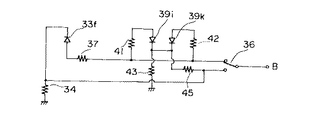
段間同調回路39は復同調回路で構成され、一次側には直列接続された二つのインダクタンス素子39a、39bが設けられ、インダクタンス素子39aがFET38のドレインに接続される。また、二次側にも直流カットコンデンサ39cを介して直列接続された二つのインダクタンス素子39d、39eが設けられ、インダクタンス素子39dが次段の混合器(図示せず)に結合される。また、インダクタンス素子39bと39eとは結合用インダクタンス素子39fに接続され、結合用インダクタンス素子39fは直流カットコンデンサ39gを介して高周波的に接地される。そして、結合用インダクタンス素子39fと直流カットコンデンサ39gとの接続点には抵抗40を介して電源電圧Bが印加される。この結果、FET38のドレインには抵抗40、インダクタンス素子39a、39b等を介して電圧が印加される。
【0005】
また、一次側のインダクタンス素子39aと39bとの接続点が直流カットコンデンサ39hを介してスイッチダイオード39iのアノードに接続され、二次側の直流カットコンデンサ39cとインダクタンス素子39eとの接続点が直流カットコンデンサ39jを介してスイッチダイオード39kのアノードに接続される。そしてスイッチダイオード39iのアノードが抵抗41を介して第二端子36bに接続され、スイッチダイオード39kのアノードが抵抗42を介して第二端子」36bに接続される。また、それらのカソードは、共に抵抗抵抗43、直流カットコンデンサ44を介して接地され、また抵抗45を介して第一端子36aに接続される。
【0006】
また、一次側にはインダクタンス素子39a、39b等に並列に接続されるバラクタダイオード39mが設けられ、二次側にもインダクタンス素子39d、39eなどに並列に接続されるバラクタダイオード39nが設けられる。それぞれのバラクタダイオード39m、39nのアノードは接地され、カソードには同調電圧が印加される。
【0007】
バンド切替回路36は入力同調回路33及び段間同調回路39をVHF帯のローバンド又はハイバンドの周波数帯に同調可能なように切り替えるためのものであり、ローバンドに同調するときには第一端子36aにハイレベルの電圧(例えば電源電圧)を出力し、ハイバンドに同調するときには第二端子36bにハイレベルの電圧を出力する。なお、バンド切替回路36は図示しない選局手段からの選局信号によって制御される。
【0008】
以上の構成において、ローバンドに同調するときには各スイッチダイオード33f、39i、39kのカソードに電圧が印加され、アノードには電圧が印加されないのでオフとなり、全てのインダクタンス素子が有効となって同調周波数バンドは低くなる。また、ハイバンドに同調するときにはスイッチダイオード33fには抵抗34を介して電流が流れてオンとなり、スイッチダイオード39i、39kには抵抗43を介して電流が流れてオンとなる。この結果、入力同調回路33においては二つのインダクタンス素子33b、33cが同調回路から外れ、段間同調回路39においては四つのインダクタンス素子39b、39e、39d、39eと結合インダクタンス素子39gとが同調回路から外れる。これによって各同調回路33、39の同調周波数バンドは高くなる。各バンドでの同調周波数は各バラクタダイオード33e、39m、39nに印加する同調電圧によって変えられる。
【0009】
【発明が解決しようとする課題】
上記の構成においては、先ず、各スイッチダイオードがオフになったときに歪みを発生するという問題があった。すなわち、図4に示すように、各スイッチダイオードは各カソードにバンド切替回路からカソードに印加される電圧によってオフとなるが、このとき各アノードには電圧が印加されない。従って、各スイッチダイオードの両端には逆方向の電圧が印加されず、いわゆる0バイアス状態となる。従って、高いレベルのテレビジョン信号が入力されると、スイッチダイオードが整流作用を起こし、此によって歪みを発生する。
【0010】
また、段間同調回路においては、スイッチダイオードをオンにするときに電流を流す抵抗43が設けられているが、この抵抗にはスイッチダイオードをオフにしたときにも電流が流れ、消費電流を大きくしていた。
【0011】
さらに、各スイッチダイオードをオン又はオフにするための直流回路には七個の抵抗を使用し、部品点数が多かった。
【0012】
そこで、本発明のテレビジョンチューナでは、スイッチダイオードをオン又はオフにするための直流回路に使用する抵抗の数を減らし、スイッチダイオードをオフにするときにはアノードとカソードとの間に逆方向の電圧が印加されるようにして大振幅のテレビジョン信号が入力されても歪みを発生しないようにすると共に、消費電流を少なくすることを目的とする。
【0013】
【課題を解決するための手段】
上記の課題を解決するための手段として、本発明のテレビジョンチューナは、入力端に結合された入力同調回路と、前記入力同調回路の次段に設けられた高周波増幅器と、前記高周波増幅器の次段に設けられた段間同調回路とを備え、前記入力同調回路及び前記段間同調回路はそれぞれ同調用インダクタンス素子と前記インダクタンス素子のインダクタンス値を切り替えるスイッチダイオードとを有するバンド切替型の同調回路で構成され、前記スイッチダイオードの各アノードにそれぞれ独立したアノード側給電抵抗を介して電源電圧を印加すると共に各アノードを電流通流手段を介して直流的に接地し、前記各カソードに各カソード側給電抵抗を介してハイレベル又はローレベルの切換電圧を印加して前記各同調回路の同調周波数帯域を切り替えた。
【0014】
また、前記高周波増幅器は増幅素子を有し、前記入力同調回路におけるスイッチダイオードのアノードを直流的に接地する前記電流通流手段を第一の抵抗とし、前記段間同調回路におけるスイッチダイオードのアノードを前記増幅素子の動作電圧印加端子に接続して前記電流通流手段を前記増幅素子とした。
【0015】
また、前記切換電圧を発生するバンド切替回路を備え、前記バンド切替回路にはオン又はオフに切り替えられるスイッチトランジスタを設け、前記スイッチトランジスタのエミッタを接地すると共に、コレクタには第二の抵抗を介して前記電源電圧を印加し、前記各カソードを前記各カソード側給電抵抗を介して前記スイッチトランジスタのコレクタに接続した。
【0016】
また、前記スイッチトランジスタと前記第二の抵抗とを前記バンド切替回路内に集積回路化した。
【0017】
【発明の実施の形態】
本発明のテレビジョンチューナの構成を図1に示す。VHF帯のローバンド及びハイバンドのテレビジョン信号が入力される入力端1には不要な信号を除去するフィルタ2を介して入力同調回路3が結合される。入力同調回路3は直列に接続された四個の同調用インダクタンス素子3a乃至3dとこれらに並列に接続される同調用バラクタダイオード3eとから構成される。また、これらのインダクタンス素子3a乃至3dの二つの接続点の間にスイッチダイオード3fの両端が高周波的に接続され、そのアノードは電流通流手段である第一の抵抗4を介して直流的に接地されると共に、第一のアノード側給電抵抗5を介して電源端子Bに接続される。また、カソードは第一のカソード側給電抵抗6を介してバンド切替回路7の出力端子7aに接続される。バラクタダイオード3eのアノードは接地され、カソードには図示はしないが同調電圧が印加される。
【0018】
入力同調回路3の次段には高周波増幅器を構成する増幅素子であると共に電流通流手段となるFET(デュアルゲートFET)8が設けられ、バラクタダイオード3eのカソードとインダクタンス素子3dとの接続点がFET8の入力端子である第一ゲートに結合される。FET8のソースは接地され、動作電圧印加端子であるドレインはFET8の次段に設けられた段間同調回路9に結合される。
【0019】
段間同調回路9は復同調回路で構成され、一次側には直列接続された二つの同調用インダクタンス素子9a、9bが設けられ、インダクタンス素子9aがFET8のドレインに接続される。また、二次側にも直流カットコンデンサ9cを間に挟んで直列接続された二つの同調用インダクタンス素子9d、9eが設けられ、インダクタンス素子9dが次段の混合器(図示せず)に結合される。また、インダクタンス素子9bと9eとは結合用インダクタンス素子9fに接続され、結合用インダクタンス素子9fは直流カットコンデンサ9gを介して高周波的に接地される。そして、結合用インダクタンス素子9fと直流カットコンデンサ9gとの接続点には第二のアノード側給電抵抗10を介して電源電圧Bが印加される。この結果、FET8のドレインには第二のアノード側給電抵抗10、インダクタンス素子9b、9a等を介して電圧が印加される。
【0020】
また、一次側のインダクタンス素子9aと9bとの接続点にスイッチダイオード9hのアノードが直接接続され、二次側の直流カットコンデンサ9cとインダクタンス素子9eとの接続点にもスイッチダイオード9iのアノードが直接接続される。そしてスイッチダイオード9hのカソードとスイッチダイオード9iのカソードとが共に直流カットコンデンサ11を介して接地され、さらに第二のカソード側給電抵抗12を介してバンド切替回路7の出力端子7aに接続される。
【0021】
また、一次側にはインダクタンス素子9a、9b等に並列に接続される同調用バラクタダイオード9jが設けられ、二次側にもインダクタンス素子9d、9e等に並列に接続される同調用バラクタダイオード9kが設けられる。それぞれのバラクタダイオード9j、9kのアノードは接地され、カソードには図示はしないが同調電圧が印加される。
【0022】
バンド切替回路7は入力同調回路3及び段間同調回路9をVHF帯のローバンド又はハイバンドの各周波数帯に同調可能なように切り替えるためのものであり、集積回路化されている。そして、スイッチトランジスタ7bと第二の抵抗7cとを内蔵し、スイッチトランジスタ7bのエミッタは接地され、コレクタは出力端子7aに接続される。また、コレクタには第二の抵抗7cを介して電源電圧が印加される。スイッチトランジスタ7bは図示しない選局手段からの選局信号によってオン又はオフに制御され、各同調回路3、9をローバンドに同調するときにはオフとなって出力端子7aをハイレベルとし、ハイバンドに同調するときにはオンとなって出力端子7aをローレベルとする。
【0023】
以上の構成における各スイッチダイオードに対する直流回路を図2に示し、上記構成の動作を説明する。まず、ローバンドに同調するときにはバンド切替回路7のスイッチトランジスタ7bがオフとなるので、各スイッチダイオード3f、9h、9iのカソードには出力端子7aから電圧が印加される。そして、入力同調回路3のスイッチダイオード3fのアノードは第一の抵抗4を介して接地されているので、第一のスイッチダイオード3fの両端には逆方向の電圧が加わり、完全にオフとなる。一方、段間同調回路9におけるスイッチダイオード9h、9iのアノードはFET8のドレインに接続されており、しかも、FET8には第二のアノード側給電抵抗10を介してドレイン電流が流れているので各スイッチダイオード9h、9iのアノード電圧は低くなっている。従って、これらスイッチダイオード9h、9iの両端にも逆方向の電圧が加わり、完全にオフとなる。この場合、段間同調回路のスイッチダイオード9h、9iのカソードには第二のカソード側給電抵抗12のみによって電圧が印加されるので、無駄な電流消費は生じない。
そして、全てのインダクタンス素子が有効となって各同調回路3、9の同調周波数バンドは低くなる。
【0024】
また、ハイバンドに同調するときにはスイッチトランジスタ7bがオンとなり、一方、入力同調回路3のスイッチダイオード3fのアノードには第一のアノード側給電抵抗5を介して電圧が印加されると共に、段間同調回路9のスイッチダイオード9h、9iのアノードには第二のアノード側給電抵抗10を介して電圧が印加される。従って、各スイッチダイオード3f、9h、9iにはスイッチトランジスタ7bを介して電流が流れてオンとなる。この結果、入力同調回路3においては二つのインダクタンス素子3b、3cが同調回路から外れ、段間同調回路9においては四つのインダクタンス素子9b、9e、9d、9eと結合インダクタンス素子9fとが同調回路から外れる。これによって各同調回路3、9の同調周波数バンドは高くなる。
【0025】
以上のように、四個の給電抵抗5、6,10、12と第一の抵抗4との五個の抵抗によって各スイッチダイオード3f、9h、9iをオン又はオフにすることが出来る。また、直流カットコンデンサの数も少なくなる。
そして、同調周波数は各バラクタダイオード3e、9j、9kに印加する同調電圧によって変えられる。
【0026】
【発明の効果】
以上のように、本発明のテレビジョンチューナは、入力同調回路及び段間同調回路はそれぞれ同調用インダクタンス素子とインダクタンス値を切り替えるスイッチダイオードとを有するバンド切替型の同調回路で構成され、スイッチダイオードの各アノードにそれぞれ独立したアノード側給電抵抗を介して電源電圧を印加すると共に各アノードを電流通流手段を介して直流的に接地し、各カソードに各カソード側給電抵抗を介してハイレベル又はローレベルの切換電圧を印加して各同調回路の同調周波数帯域を切り替えたので、各スイッチダイオードをオフにするときには両端に逆方向の電圧が加わって完全にオフとなり、大振幅のテレビジョン信号に対しても歪みを発生しない。また、段間同調回路のスイッチダイオードのカソードにはカソード側給電抵抗のみによって電圧が印加されるので、無駄な電流消費は生じない。さらに、スイッチダイオードに電圧を印加する給電抵抗の数や直流カットコンデンサの数が削減出来る。さらに、バンド切替回路の出力端子が最低の一個で済むのでコストを下げられる。
【0027】
また、入力同調回路におけるスイッチダイオードのアノードを直流的に接地する電流通流手段を第一の抵抗とし、段間同調回路におけるスイッチダイオードのアノードを増幅素子の動作電圧印加端子に接続して電流通流手段を増幅素子としたことによって、段間同調回路におけるスイッチダイオードのアノードは増幅素子に流れる電流によって低くなるので、このスイッチダイオードの両端には簡単に逆方向の電圧を加えることが出来る。
【0028】
また、切換電圧を発生するバンド切替回路を備え、バンド切替回路にはオン又はオフに切り替えられるスイッチトランジスタを設け、スイッチトランジスタのエミッタを接地すると共に、コレクタには第二の抵抗を介して電源電圧を印加し、各カソードを各カソード側給電抵抗を介してスイッチトランジスタのコレクタに接続したので、スイッチトランジスタをオンにすることで各スイッチダイオードの電流をスイッチトランジスタに流すことができる。
【0029】
また、スイッチトランジスタと第二の抵抗とをバンド切替回路内に集積回路化したので、切換電圧が簡単に得られる。
【図面の簡単な説明】
【図1】本発明のテレビジョンチューナの構成を示す回路図である。
【図2】本発明のテレビジョンチューナにおけるスイッチダイオードに対する直流回路図である。
【図3】従来のテレビジョンチューナの構成を示す回路図である。
【図4】従来のテレビジョンチューナにおけるスイッチダイオードに対する直流回路図である。
【符号の説明】
1 入力端
2 フィルタ
3 入力同調回路
3a〜3d 同調用インダクタンス素子
3e 同調用バラクタダイオード
3f スイッチダイオード
4 第一の抵抗(電流通流手段)
5 第一のアノード側給電抵抗
6 第一のカソード側給電抵抗
7 バンド切替回路
7a 出力端子
7b スイッチトランジスタ
7c 第二の抵抗
8 FET(電流通流手段)
9 段間同調回路
9a、9b、9d、9e 同調用インダクタンス素子
9c、9g 直流カットコンデンサ
9f 結合用インダクタンス素子
9h、9i スイッチダイオード
9j、9k 同調用バラクタダイオード
10 第二のアノード側給電抵抗
11 直流カットコンデンサ
12 第二のカソード側給電抵抗[0001]
BACKGROUND OF THE INVENTION
The present invention relates to a television tuner for receiving a VHF band television signal.
[0002]
[Prior art]
The configuration of a conventional television tuner is shown in FIG. An
[0003]
The next stage of the
[0004]
The
[0005]
Further, the connection point between the primary side inductance elements 39a and 39b is connected to the anode of the switch diode 39i via the DC cut capacitor 39h, and the connection point between the secondary side
[0006]
Further, a
[0007]
The
[0008]
In the above configuration, when tuning to the low band, a voltage is applied to the cathodes of the
[0009]
[Problems to be solved by the invention]
In the above configuration, first, there is a problem that distortion occurs when each switch diode is turned off. That is, as shown in FIG. 4, each switch diode is turned off by a voltage applied to the cathode from the band switching circuit to each cathode, but at this time, no voltage is applied to each anode. Therefore, a reverse voltage is not applied to both ends of each switch diode, and a so-called zero bias state is established. Therefore, when a high level television signal is input, the switch diode causes rectification, which causes distortion.
[0010]
Further, in the interstage tuning circuit, a
[0011]
Furthermore, seven resistors are used in the DC circuit for turning on or off each switch diode, and the number of parts is large.
[0012]
Therefore, in the television tuner of the present invention, the number of resistors used in the DC circuit for turning on or off the switch diode is reduced, and when the switch diode is turned off, a reverse voltage is applied between the anode and the cathode. An object is to prevent distortion even when a large-amplitude television signal is input as it is applied, and to reduce current consumption.
[0013]
[Means for Solving the Problems]
As means for solving the above-described problems, a television tuner of the present invention includes an input tuning circuit coupled to an input terminal, a high-frequency amplifier provided at the next stage of the input tuning circuit, and a next to the high-frequency amplifier. An interstage tuning circuit provided in a stage, and each of the input tuning circuit and the interstage tuning circuit is a band switching type tuning circuit having a tuning inductance element and a switch diode for switching an inductance value of the inductance element. The power supply voltage is applied to each anode of the switch diode via an independent anode-side power supply resistor, and each anode is grounded in a DC manner through a current flow means, and each cathode-side power is supplied to each cathode. Applying a high-level or low-level switching voltage via a resistor to adjust the tuning frequency band of each tuning circuit. Ri was replaced.
[0014]
The high-frequency amplifier includes an amplifying element, and the current passing means for DC-grounding the anode of the switch diode in the input tuning circuit is a first resistor, and the anode of the switch diode in the interstage tuning circuit is The current passing means is connected to the operating voltage application terminal of the amplifying element as the amplifying element.
[0015]
The band switching circuit for generating the switching voltage is provided. The band switching circuit is provided with a switch transistor that can be switched on or off. The emitter of the switch transistor is grounded, and the collector is connected via a second resistor. The power supply voltage was applied, and each cathode was connected to the collector of the switch transistor via each cathode-side power supply resistor.
[0016]
The switch transistor and the second resistor are integrated in the band switching circuit.
[0017]
DETAILED DESCRIPTION OF THE INVENTION
The configuration of the television tuner of the present invention is shown in FIG. An input tuning circuit 3 is coupled to an input terminal 1 to which a VHF band low-band and high-band television signal is input via a
[0018]
The next stage of the input tuning circuit 3 is provided with an FET (dual gate FET) 8 which is an amplifying element constituting a high frequency amplifier and serves as a current passing means, and a connection point between the cathode of the varactor diode 3e and the inductance element 3d is provided. It is coupled to the first gate which is the input terminal of the FET 8. The source of the FET 8 is grounded, and the drain which is an operating voltage application terminal is coupled to an interstage tuning circuit 9 provided at the next stage of the FET 8.
[0019]
The interstage tuning circuit 9 is composed of a post-tuning circuit. On the primary side, two tuning inductance elements 9 a and 9 b connected in series are provided, and the inductance element 9 a is connected to the drain of the FET 8. Also, two tuning
[0020]
The anode of the
[0021]
A tuning varactor diode 9j connected in parallel to the inductance elements 9a and 9b is provided on the primary side, and a tuning varactor diode 9k connected in parallel to the
[0022]
The
[0023]
FIG. 2 shows a DC circuit for each switch diode in the above configuration, and the operation of the above configuration will be described. First, since the switch transistor 7b of the
And all the inductance elements become effective, and the tuning frequency band of each tuning circuit 3 and 9 becomes low.
[0024]
When tuning to the high band, the switch transistor 7b is turned on. On the other hand, a voltage is applied to the anode of the switch diode 3f of the input tuning circuit 3 via the first anode-side
[0025]
As described above, the
The tuning frequency is changed by the tuning voltage applied to each varactor diode 3e, 9j, 9k.
[0026]
【The invention's effect】
As described above, in the television tuner of the present invention, the input tuning circuit and the interstage tuning circuit are each composed of a band switching type tuning circuit having a tuning inductance element and a switching diode for switching an inductance value. A power supply voltage is applied to each anode via an independent anode-side power supply resistor, and each anode is grounded in a direct current manner via a current flow means, and each cathode is connected to a high level or a low level via each cathode-side power supply resistor. Since the tuning frequency band of each tuning circuit was switched by applying a level switching voltage, when turning off each switch diode, a reverse voltage was applied to both ends to completely turn it off, and for a large amplitude television signal Even without distortion. Further, since a voltage is applied only to the cathode of the switch diode of the interstage tuning circuit by the cathode side feeding resistor, no wasteful current consumption occurs. Furthermore, the number of power supply resistors for applying a voltage to the switch diode and the number of DC cut capacitors can be reduced. Furthermore, since the output terminal of the band switching circuit can be at least one, the cost can be reduced.
[0027]
In addition, the current passing means for grounding the anode of the switch diode in the input tuning circuit in a DC manner is a first resistor, and the anode of the switch diode in the interstage tuning circuit is connected to the operating voltage application terminal of the amplifying element. By using the amplifying element as the flow means, the anode of the switch diode in the interstage tuning circuit is lowered by the current flowing through the amplifying element, so that a reverse voltage can be easily applied to both ends of the switch diode.
[0028]
In addition, a band switching circuit for generating a switching voltage is provided. The band switching circuit is provided with a switch transistor that can be switched on or off. The emitter of the switch transistor is grounded, and the power supply voltage is connected to the collector through a second resistor. Since each cathode is connected to the collector of the switch transistor via each cathode-side power supply resistor, the current of each switch diode can be passed through the switch transistor by turning on the switch transistor.
[0029]
Further, since the switch transistor and the second resistor are integrated in the band switching circuit, the switching voltage can be easily obtained.
[Brief description of the drawings]
FIG. 1 is a circuit diagram showing a configuration of a television tuner of the present invention.
FIG. 2 is a DC circuit diagram for a switch diode in the television tuner of the present invention.
FIG. 3 is a circuit diagram showing a configuration of a conventional television tuner.
FIG. 4 is a DC circuit diagram for a switch diode in a conventional television tuner.
[Explanation of symbols]
DESCRIPTION OF SYMBOLS 1
5 First anode side feeding resistor 6 First cathode
9
Claims (4)
Priority Applications (7)
| Application Number | Priority Date | Filing Date | Title |
|---|---|---|---|
| JP2000384917A JP3828745B2 (en) | 2000-12-14 | 2000-12-14 | Television tuner |
| MYPI20015546A MY126827A (en) | 2000-12-14 | 2001-12-05 | Television tuner having less distortion |
| EP01310237A EP1217737B1 (en) | 2000-12-14 | 2001-12-07 | Television tuner |
| DE60117732T DE60117732T2 (en) | 2000-12-14 | 2001-12-07 | TV tuner |
| KR10-2001-0078763A KR100407493B1 (en) | 2000-12-14 | 2001-12-13 | Television tuner |
| CNB011403268A CN1187966C (en) | 2000-12-14 | 2001-12-13 | Television tuner |
| US10/017,433 US6864925B2 (en) | 2000-12-14 | 2001-12-14 | Television tuner having less distortion |
Applications Claiming Priority (1)
| Application Number | Priority Date | Filing Date | Title |
|---|---|---|---|
| JP2000384917A JP3828745B2 (en) | 2000-12-14 | 2000-12-14 | Television tuner |
Publications (2)
| Publication Number | Publication Date |
|---|---|
| JP2002185878A JP2002185878A (en) | 2002-06-28 |
| JP3828745B2 true JP3828745B2 (en) | 2006-10-04 |
Family
ID=18852278
Family Applications (1)
| Application Number | Title | Priority Date | Filing Date |
|---|---|---|---|
| JP2000384917A Expired - Fee Related JP3828745B2 (en) | 2000-12-14 | 2000-12-14 | Television tuner |
Country Status (7)
| Country | Link |
|---|---|
| US (1) | US6864925B2 (en) |
| EP (1) | EP1217737B1 (en) |
| JP (1) | JP3828745B2 (en) |
| KR (1) | KR100407493B1 (en) |
| CN (1) | CN1187966C (en) |
| DE (1) | DE60117732T2 (en) |
| MY (1) | MY126827A (en) |
Families Citing this family (5)
| Publication number | Priority date | Publication date | Assignee | Title |
|---|---|---|---|---|
| JP3096170U (en) * | 2003-02-27 | 2003-09-05 | アルプス電気株式会社 | Television tuner input circuit |
| JP3101830U (en) * | 2003-11-21 | 2004-06-24 | アルプス電気株式会社 | Band switching type tuning circuit |
| JP3103017U (en) * | 2004-01-27 | 2004-07-22 | アルプス電気株式会社 | Television tuner |
| JP3106152U (en) * | 2004-06-24 | 2004-12-16 | アルプス電気株式会社 | Television tuner |
| KR20090003013A (en) * | 2007-07-05 | 2009-01-09 | 엘지이노텍 주식회사 | Input resonance circuit of tuner |
Family Cites Families (18)
| Publication number | Priority date | Publication date | Assignee | Title |
|---|---|---|---|---|
| JPS5330212Y2 (en) * | 1972-09-22 | 1978-07-28 | ||
| JPS51118301A (en) * | 1975-04-11 | 1976-10-18 | Hitachi Ltd | Circuit distribution for switching tuner s receiving frequency band |
| JPS6040216B2 (en) * | 1977-03-31 | 1985-09-10 | 株式会社村田製作所 | tv jiyeon chiyuna |
| US4189678A (en) * | 1977-08-18 | 1980-02-19 | Sanyo Electric Co., Ltd. | Combination VHF-UHF tuner for use in a television receiver |
| JPS6038063B2 (en) * | 1978-05-29 | 1985-08-29 | 株式会社日立製作所 | TV tuner circuit |
| JPS6121882Y2 (en) * | 1980-11-14 | 1986-07-01 | ||
| JPS5899927U (en) * | 1981-12-25 | 1983-07-07 | アルプス電気株式会社 | Tuner band switching circuit |
| JPS6352510A (en) * | 1986-08-22 | 1988-03-05 | Toshiba Corp | Electronic tuner |
| JP2956098B2 (en) * | 1989-12-20 | 1999-10-04 | 松下電器産業株式会社 | Television tuner |
| DE4028572A1 (en) * | 1990-09-08 | 1992-03-12 | Telefunken Sendertechnik | Electronically switched resonance circuit with extra capacitor - has switching diode energised by diode polarised in control line for control voltage flow |
| JPH0993091A (en) | 1995-09-25 | 1997-04-04 | Alps Electric Co Ltd | Input tuning circuit of television tuner |
| JP3264811B2 (en) * | 1995-11-20 | 2002-03-11 | アルプス電気株式会社 | Voltage control variable tuning circuit |
| JPH104315A (en) * | 1996-06-14 | 1998-01-06 | Matsushita Electric Ind Co Ltd | High frequency oscillation circuit |
| JP3250785B2 (en) * | 1996-08-09 | 2002-01-28 | アルプス電気株式会社 | TV tuner |
| JPH11205700A (en) * | 1998-01-12 | 1999-07-30 | Alps Electric Co Ltd | Double-tuning circuit |
| DE19819544A1 (en) * | 1998-04-30 | 1999-11-11 | Siemens Ag | Circuit arrangement for range switching in high-frequency receivers |
| JP3612241B2 (en) * | 1999-05-31 | 2005-01-19 | アルプス電気株式会社 | Intermediate frequency circuit of television tuner |
| JP2001156593A (en) * | 1999-12-01 | 2001-06-08 | Alps Electric Co Ltd | Input circuit for television power |
-
2000
- 2000-12-14 JP JP2000384917A patent/JP3828745B2/en not_active Expired - Fee Related
-
2001
- 2001-12-05 MY MYPI20015546A patent/MY126827A/en unknown
- 2001-12-07 EP EP01310237A patent/EP1217737B1/en not_active Expired - Lifetime
- 2001-12-07 DE DE60117732T patent/DE60117732T2/en not_active Expired - Lifetime
- 2001-12-13 KR KR10-2001-0078763A patent/KR100407493B1/en not_active IP Right Cessation
- 2001-12-13 CN CNB011403268A patent/CN1187966C/en not_active Expired - Fee Related
- 2001-12-14 US US10/017,433 patent/US6864925B2/en not_active Expired - Fee Related
Also Published As
| Publication number | Publication date |
|---|---|
| US20020075414A1 (en) | 2002-06-20 |
| CN1359233A (en) | 2002-07-17 |
| JP2002185878A (en) | 2002-06-28 |
| US6864925B2 (en) | 2005-03-08 |
| DE60117732T2 (en) | 2006-11-09 |
| KR100407493B1 (en) | 2003-11-28 |
| EP1217737A1 (en) | 2002-06-26 |
| DE60117732D1 (en) | 2006-05-04 |
| EP1217737B1 (en) | 2006-03-08 |
| KR20020046991A (en) | 2002-06-21 |
| MY126827A (en) | 2006-10-31 |
| CN1187966C (en) | 2005-02-02 |
Similar Documents
| Publication | Publication Date | Title |
|---|---|---|
| US20080116974A1 (en) | Pulse amplifier | |
| JP3828745B2 (en) | Television tuner | |
| US7509111B2 (en) | Integrated circuit having a mixer circuit | |
| JPH07107961B2 (en) | Local oscillator for television receiver | |
| US6903783B2 (en) | Tuner for receiving television signal in VHF band and UHF band | |
| JPH11205700A (en) | Double-tuning circuit | |
| US6904271B2 (en) | High-frequency-signal switching circuit suppressing high-frequency-signal distortion | |
| US7412219B2 (en) | High-frequency amplifier having simple circuit structure and television tuner using high-frequency amplifier | |
| US6900850B2 (en) | Television tuner having simplified wiring for interconnection and having miniaturized integrated circuit | |
| US7398070B2 (en) | Variable gain amplifying circuit with matchable input/output impedance | |
| JP3101830U (en) | Band switching type tuning circuit | |
| JP3979519B2 (en) | Television tuner | |
| JP2007068069A (en) | Tuner circuit | |
| JP4024541B2 (en) | Integrated circuit for tuner and television tuner using the integrated circuit for tuner | |
| JP3847122B2 (en) | Television tuner band switching circuit | |
| JP3105564U (en) | Television tuner | |
| JP3891926B2 (en) | Television signal switching circuit | |
| JP3765974B2 (en) | Television tuner | |
| US7414675B2 (en) | Television tuner being capable of receiving FM broadcast signal | |
| JP3106226U (en) | Television tuner | |
| JP3713419B2 (en) | Band switching voltage generation circuit and television tuner using the band switching voltage generation circuit | |
| JP3100212U (en) | Television tuner | |
| JP3095332U (en) | Band switching type tuning circuit | |
| JP3106152U (en) | Television tuner | |
| JP2001211397A (en) | High frequency tuning circuit |
Legal Events
| Date | Code | Title | Description |
|---|---|---|---|
| A977 | Report on retrieval |
Free format text: JAPANESE INTERMEDIATE CODE: A971007 Effective date: 20060126 |
|
| A131 | Notification of reasons for refusal |
Free format text: JAPANESE INTERMEDIATE CODE: A131 Effective date: 20060328 |
|
| A521 | Written amendment |
Free format text: JAPANESE INTERMEDIATE CODE: A523 Effective date: 20060523 |
|
| RD03 | Notification of appointment of power of attorney |
Free format text: JAPANESE INTERMEDIATE CODE: A7423 Effective date: 20060523 |
|
| TRDD | Decision of grant or rejection written | ||
| A01 | Written decision to grant a patent or to grant a registration (utility model) |
Free format text: JAPANESE INTERMEDIATE CODE: A01 Effective date: 20060620 |
|
| A61 | First payment of annual fees (during grant procedure) |
Free format text: JAPANESE INTERMEDIATE CODE: A61 Effective date: 20060707 |
|
| R150 | Certificate of patent or registration of utility model |
Free format text: JAPANESE INTERMEDIATE CODE: R150 |
|
| FPAY | Renewal fee payment (event date is renewal date of database) |
Free format text: PAYMENT UNTIL: 20100714 Year of fee payment: 4 |
|
| FPAY | Renewal fee payment (event date is renewal date of database) |
Free format text: PAYMENT UNTIL: 20110714 Year of fee payment: 5 |
|
| FPAY | Renewal fee payment (event date is renewal date of database) |
Free format text: PAYMENT UNTIL: 20120714 Year of fee payment: 6 |
|
| FPAY | Renewal fee payment (event date is renewal date of database) |
Free format text: PAYMENT UNTIL: 20130714 Year of fee payment: 7 |
|
| LAPS | Cancellation because of no payment of annual fees |