JP3825862B2 - Synchronous dynamic semiconductor memory device - Google Patents
Synchronous dynamic semiconductor memory device Download PDFInfo
- Publication number
- JP3825862B2 JP3825862B2 JP04388897A JP4388897A JP3825862B2 JP 3825862 B2 JP3825862 B2 JP 3825862B2 JP 04388897 A JP04388897 A JP 04388897A JP 4388897 A JP4388897 A JP 4388897A JP 3825862 B2 JP3825862 B2 JP 3825862B2
- Authority
- JP
- Japan
- Prior art keywords
- signal
- clock signal
- wiring
- data
- external
- Prior art date
- Legal status (The legal status is an assumption and is not a legal conclusion. Google has not performed a legal analysis and makes no representation as to the accuracy of the status listed.)
- Expired - Fee Related
Links
Images


Classifications
-
- G—PHYSICS
- G11—INFORMATION STORAGE
- G11C—STATIC STORES
- G11C11/00—Digital stores characterised by the use of particular electric or magnetic storage elements; Storage elements therefor
- G11C11/21—Digital stores characterised by the use of particular electric or magnetic storage elements; Storage elements therefor using electric elements
- G11C11/34—Digital stores characterised by the use of particular electric or magnetic storage elements; Storage elements therefor using electric elements using semiconductor devices
- G11C11/40—Digital stores characterised by the use of particular electric or magnetic storage elements; Storage elements therefor using electric elements using semiconductor devices using transistors
- G11C11/401—Digital stores characterised by the use of particular electric or magnetic storage elements; Storage elements therefor using electric elements using semiconductor devices using transistors forming cells needing refreshing or charge regeneration, i.e. dynamic cells
- G11C11/4063—Auxiliary circuits, e.g. for addressing, decoding, driving, writing, sensing or timing
- G11C11/407—Auxiliary circuits, e.g. for addressing, decoding, driving, writing, sensing or timing for memory cells of the field-effect type
-
- G—PHYSICS
- G11—INFORMATION STORAGE
- G11C—STATIC STORES
- G11C7/00—Arrangements for writing information into, or reading information out from, a digital store
- G11C7/22—Read-write [R-W] timing or clocking circuits; Read-write [R-W] control signal generators or management
-
- G—PHYSICS
- G11—INFORMATION STORAGE
- G11C—STATIC STORES
- G11C7/00—Arrangements for writing information into, or reading information out from, a digital store
- G11C7/10—Input/output [I/O] data interface arrangements, e.g. I/O data control circuits, I/O data buffers
- G11C7/1051—Data output circuits, e.g. read-out amplifiers, data output buffers, data output registers, data output level conversion circuits
Description
【0001】
【発明の属する技術分野】
この発明は、外部クロック信号に同期して動作する同期型ダイナミック型半導体記憶装置に関し、特に、外部クロック信号に応じて、データ読出動作を制御する同期型ダイナミック型半導体記憶装置の構成に関する。
【0002】
【従来の技術】
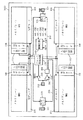
図17は、従来のLOC(リード・オン・チップ)構造に適したパッド配置を有する半導体記憶装置のチップレイアウトを概略的に示す図である。図17において、半導体記憶装置チップ1の第2の方向(以下、単に短辺方向と称す)の中央領域CRに、第1の方向(以下、単に長辺方向と称す)に沿ってパッドPDが整列して配置される。この半導体記憶装置チップ1の中央領域CRの両側に、メモリセルアレイを含むメモリセルプレーンM♯0〜M♯3が配置される。パッドPDは、この半導体記憶装置チップ1上にわたって中央部にまで延在するリードフレームFRと、中央領域CR近傍でボンディングワイヤにより接続される。
【0003】
すなわち、LOC構造においては、パッケージの外部端子と接続されているリードフレームが、チップの上面に載る構造となる。従来は、リードフレームの上部にチップが載る構造であるため、リードフレーム端のボンディング部分からチップ周辺部にあるボンディングパッド部に、金線でボンディングせざるを得ず、収容するチップサイズに上限があった。
【0004】
LOC構造では、リードフレームをチップ上に覆いかぶさるようにチップ中央部まで延長し、そこからボンディングできるので、チップ上のボンディングパッドの位置を従来のチップ周辺部からチップの中央部に移すことが可能である。このため、収容できるチップサイズを大きくしたり、パッケージ端子の自己インダクタンスや静電容量を小さくすることが可能である。さらには、チップのボンディングパッドからバッファ回路までのアルミ引出し線を短くできるので、この部分の配線遅延を短くすることも可能である。さらには後述するように、ボンディングパッドと周辺回路の両者をチップの真ん中に十字形に配置することが可能で、周辺回路内の回路ブロック間の平均的な配線長を最も短くすることができ、高速設計を行なうことが容易となる。
【0005】
すなわち、図17に示したように、半導体記憶装置チップ1は、ボンディングパッドと周辺回路を、メモリセルプレーンM♯0〜M♯3を配置した後の空き領域であるチップ中央部の十字領域に配置した構成となっている。このような構成は、以下に説明するように周辺回路の配線遅延を減らすために有効である。
【0006】
周辺回路内の遅延を減らすために回路の配置および配線の配置において留意すべきことは、ボンディングパッドと入出力パッドを近接配置すること、関連回路を集中・近接配置して速度を支配する信号経路(クリティカル・パス)の配線をできるだけ局所化すること、クリティカル・パスでない信号はできるだけグローバル配線に回すこと、それでもグローバル配線がクリティカル・パスになる場合は、その長さができるだけ短くなるように周辺回路全体の配置を行なうこと、などである。
【0007】
行と列のいずれの方向から見ても、上述したようなこれらの条件をすべて満足させる場合には、ボンディングパッドと周辺回路を行の中心と列の中心に配置する、すなわちそれらをチップの中心部に十字形に配置・配線するのが望ましい。
【0008】
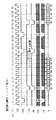
図18は、JEDEC(Joint Electron device Engineering Council)の基準により標準化された、256MDRAMのパッケージのピン配置を示す模式図である。
【0009】
図18に示したピン配置の標準においては、アクセス時間の高速化を目的として、パッケージのピン配置においては、クロック信号、コントロール信号(たとえば、ext./RAS,ext./CASなど)、アドレス信号用のピンを、パッケージの両端部側に配置されたデータ入出力用のDQピンの内側に配置する構成となっている。
【0010】
この構成においては、外部クロック信号(ext.CLK)ピンは、パッケージの中心位置、すなわち、同期型ダイナミック型半導体記憶装置のチップ中心よりもずれた位置に存在する(ピン番号50番または51番)。
【0011】
このように、外部クロック信号入力ピンがチップ中心部よりもずれた位置に存在することは、以下に説明するように、同期型ダイナミック型半導体記憶装置のデータ出力動作において、信号のスキューの発生等の問題をもたらし、このことが動作速度の向上を阻害する要因となる。
【0012】
以下では、従来の同期型ダイナミック型半導体記憶装置の動作について簡単に説明する。
【0013】
一般に、主記憶として用いられるダイナミック型ランダムアクセスメモリ(以下、DRAMと呼ぶ。)は高速化されてはいるものの、その動作速度はマイクロプロセッサ(以下、MPUと呼ぶ。)の動作速度に追随することはできない。このために、DRAMのアクセスタイムおよびサイクルタイムがボトルネックとなりシステム全体の性能が低下するという問題点が従来存在した。近年、高速MPUのための主記憶としてクロック信号に同期して動作する同期型DRAM(同期型ダイナミック型ランダムアクセスメモリ:以下、適宜SDRAMと呼ぶ。)がシステムに用いられるようになっている。
【0014】
SDRAMにおいては、高速でアクセスするために、システムクロック信号(外部クロック信号)に同期して、連続した、たとえば1つのデータ入出力端子当り8ビットの連続ビットにアクセスする仕様が存在する。この連続アクセスの仕様を満たす標準的なタイミングチャートを図19に示す。図19においては、データ入出力端子DQ0ないしDQ7の8ビット(1バイト)のデータ入力および出力が可能なSDRAMにおいて、連続して8ビットのデータを読出す動作を示している。すなわち、8ビット×8=64ビットのデータを連続して書込むことが可能である。
【0015】
連続して、読出あるいは書込が行なわれるデータのビット数はバースト長BLと呼ばれ、SDRAMにおいては、モードレジスタによって変更することが可能である。
【0016】
図19に示すように、SDRAMにおいては、たとえば外部からのクロック信号CLKの立上がりエッジで外部からの制御信号、すなわちロウアドレスストローブ信号/RAS、コラムアドレスストローブ信号/CAS、アドレス信号Addとが取込まれる。
【0017】
アドレス信号Addは、時分割的に多重化された行アドレス信号Xaと列アドレス信号Ybを含む。
【0018】
サイクル1におけるクロック信号CLKの立上がりのエッジにおいて、外部ロウアドレスストローブ信号ext./RASが活性状態の“L”レベル、外部コラムアドレスストローブ信号ext./CASおよび外部ライトイネーブル信号ext./WEが“H”レベルであれば、そのときのアドレス信号Addが行アドレス信号のXaとして取込まれる。
【0019】
次いで、サイクル4におけるクロック信号CLKの立上がりのエッジにおいて、外部コラムアドレスストローブ信号ext./CASが活性状態である“L”レベルにあれば、そのときのアドレス信号Addが列アドレス信号Ybとして取込まれる。この取込まれた行アドレス信号Xaおよび列アドレス信号Ybに従って、SDRAM内において行および列の選択動作が実施される。外部ロウアドレスストローブ信号ext./RASが“L”レベルに立下がってから、所定のクロック期間(図19においては6クロックサイクル)が経過した後、データ入出力端子DQから出力される8ビットデータのうちの最初のデータb0が出力される。
【0020】
以後、クロック信号CLKの立上がりに応答して、データb1〜b7が出力される。
【0021】
図20は、SDRAMにおいて、1つのデータ入出力端子DQ当り連続して8ビットのデータを書込む動作を行なう場合の外部信号の状態を示すタイミングチャートである。
【0022】
書込動作においては、行アドレス信号Xaの取込はデータ読出時と同様である。すなわち、サイクル1におけるクロック信号CLKの立上がりエッジにおいて信号ext./RASが活性状態の“L”レベル、信号ext./CASおよびext.WEが“H”レベルであれば、そのときのアドレス信号Addが行アドレス信号Xaとして取込まれる。
【0023】
サイクル4におけるクロック信号CLKの立上がりのエッジにおいて、信号ext./CASおよびext./WEがともに活性状態の“L”レベルであれば、列アドレス信号Ybが取込まれるとともに、そのときにデータ入出力端子DQに与えられていたデータb0が、連続して書込まれた8ビットのデータのうち最初の書込データとして取込まれる。
【0024】
この信号ext./RASおよびext./CASの立上がりエッジに応答してSDRAM内において行および列選択動作が実行される。以後は、クロック信号CLKに同期して、順次入力データb1〜b7が取込まれ、順次対応するメモリセルにこの入力データが書込まれていく。
【0025】
上述のように、SDRAMにおいては、従来のDRAMにおけるロウアドレスストローブ信号ext./RASおよびコラムアドレスストローブ信号ext./CASという外部制御信号に同期してアドレス信号および入力データなどを取込んで動作させる方式と異なり、外部から与えられるシステムクロックであるクロック信号CLKの立上がりエッジで、アドレスストローブ信号ext./RAS、ext./CAS、アドレス信号および入力データなどの外部信号の取込が行なわれる。
【0026】
このように、SDRAMは、外部からのクロック信号に同期して、制御信号およびデータ信号を取込む同期動作を行なうので、アドレス信号のスキュー(タイミングのずれ)によるデータ入出力時間に対するマージンを確保する必要がない。したがって、サイクルタイムを短縮することができるという利点を有する。このように、クロック信号に同期して連続データの書込および読出を実行することができるため、連続したアドレスに対して連続アクセスを行なう場合のアクセスタイムの短縮が可能となる。
【0027】
図21は、従来のSDRAM4000の構成の一部を示す概略ブロック図である。
【0028】
図21においては、図17において示した複数のパッドPDのうち、チップの短辺近傍にそれぞれ存在する2つのデータ入出力端子DQと、外部クロック信号ext.CLKが入力される外部クロック入力端子の3つの入出力端子のみを示し、他の入出力端子、たとえば、アドレス信号入力端子等は図示省略している。
【0029】
従来のSDRAM4000は、4つのメモリセルプレーンM♯0〜M♯3に分割されたメモリセルアレイと、各メモリセルプレーンごとに設けられ、外部から与えられる行アドレス信号Xaに応じて、対応する行の選択を行なう行デコーダ106と、各メモリセルプレーンごとに設けられ、外部から与えられる列アドレス信号Ybに応じて、対応する列の選択を行なう列デコーダ108と、外部から与えられる制御信号、チップセレクト信号ext./CS、クロックイネーブル信号ext.CKE、ロウアドレスストローブ信号ext./RAS、コラムアドレスストローブ信号ext./CAS、ライトイネーブル信号ext./WE等を受けて、内部回路の読出動作および書込動作を制御する制御回路100と、外部クロック入力パッド112を介して与えられる外部クロック信号ext./CLKを受ける初段の入力バッファ回路104と、初段入力バッファ回路104の出力を、配線116を介して受け、内部クロック信号を発生するクロック発生回路102と、外部から選択されたメモリセルから読出され、入出力回路110を介して出力される読出データを受け、クロック発生回路102からの内部クロック信号に同期して、読出データを出力する出力バッファ118と、出力バッファ118の出力を受けて、読出データを出力するデータ入出力パッド114とを含む。
【0030】
以下では、便宜上チップ左側に存在するデータ入出力パッドを特にDQLで、チップ右側に存在するデータ入出力パッドをDQRで表わすことにする。
【0031】
ここで、上記制御信号のうち、信号ext./CKEは、それが活性状態(“L”レベル)である期間は、セルフリフレッシュモードであることを指定するための信号であり、信号ext./CSは、それが活性状態(“L”レベル)であるときに、制御信号を読取むことを指示する信号であり、ext./RASは、それが活性状態(“L”レベル)のときに、行系の回路の動作を活性状態とすることを指示するための信号であり、信号ext./CASは、それが活性状態(“L”レベル)であるときに、列系の回路の動作を活性とすることを指示するための信号であり、信号ext./WEは、それが活性状態となることで、データ書込モードの開始を指定するための信号である。
【0032】
ただし、上述したような各制御信号の機能は、原則的なものであって、それらの特殊な組合せによっては、後に説明するように、制御回路100に対して、一定の動作モードの開始または終了を指示することになる。
【0033】
一般的には、信号の入出力を行なうパッド近傍に入力初段バッファ回路を設置し、その出力をチップ中央付近に存在するマスタ制御回路群に入力して、このマスタ制御回路群がチップ全体を制御する信号を発生する。このような構成は、内部クロック発生回路102に対しても一般に用いられており、外部クロック入力パッド112近傍にある入力初段回路104は、外部から与えられる外部クロック信号を外部レベル(たとえば、フルスイングで5V)から、チップ内部レベル(たとえば、フルスイングで3.3V)にレベル変換した後、マスタ制御回路群内にあるクロック発生回路102に対して、外部クロック信号を伝達する。
【0034】
クロック発生回路102は、クロック信号のパルス幅の調整とともに、チップ内部に使用目的に応じた内部クロック信号を供給する。この内部クロック信号が供給される相手側の回路としては、大まかに分類すると、ロウ系回路、コラム系回路、データ出力系回路等が存在する。
【0035】
すなわち、SDRAM等の外部クロック同期型メモリにおいては、外部クロック信号に同期しつつ、行選択動作、列選択動作、データ読出動作、データ出力動作等が行なわれることになるが、このうち、データ出力系回路に供給される内部クロック信号を、データ出力パッド114に対するデータ出力バッファ回路118に対して、いかに短い遅延時間で到達させるかがチップ性能に大きく関係している。
【0036】
つまり、このデータ出力バッファに対する内部クロック信号供給の高速化は、チップのアクセス時間等の性能向上のための重要なポイントとなる。
【0037】
【発明が解決しようとする課題】
図21に示すように、従来のSDRAM4000においては、外部クロック信号入力パッド112から、一旦チップ中央付近まで、この外部クロック信号が伝達された後、クロック発生回路102が、データ出力バッファに対する内部クロック信号と他のロウ系またはコラム系回路に対して供給する内部クロック信号とを同時に発生する構成となっている。
【0038】
したがって、データ出力バッファに対して与える内部クロック信号を高速化するためには、入力初段バッファ回路104を構成するトランジスタの電流駆動能力を大きくする必要がある。このことは、言い換えると、入力初段バッファ回路104を構成するトランジスタサイズ(ゲート幅)を大きくする必要があることを意味する。
【0039】
しかしながら、入力初段バッファ回路104は、他の内部クロック信号についても共有される構成となっているため、SDRAM4000が動作中は、常にこの入力初段バッファ回路104は大電流を消費することになる。
【0040】
図22は、外部クロック信号入力パッド112および入力初段バッファ回路104ならびにクロック発生回路102のみを構成部分を抽出して示した概略ブロック図である。
【0041】
図18に示したようなピン配置の標準に対応して、チップ内にパッドを配置した場合、外部クロック信号入力パッド112の近傍に設けられている入力初段バッファ回路104から、チップ中央部に設けられているクロック発生回路102とを接続する配線116の配線長lは、1〜2mmに達する場合がある。
【0042】
したがって、上述したとおり、入力初段バッファ回路104は、この比較的長い配線116を駆動するだけの電流駆動能力が必要となる。
【0043】
図23は、初段入力バッファ回路104および内部クロック発生回路102の構成を示す概略ブロック図である。
【0044】
図23に示すように、入力初段回路104は、差動増幅回路1042と、ドライバ回路1044とを含む。
【0045】
差動増幅回路1042は、一方の入力端に、基準電位Vrefを受け、他の入力端に、外部クロック入力パッド112からの外部クロック信号の電位レベルを受ける構成となっている。また、差動増幅回路1042は、電源パワーオフ時に活性状態(“L”レベル)となるパワーダウンモード活性化信号/PDEにより制御される構成となっている。
【0046】
すなわち、SDRAM4000に対して、電源供給が開始され、パワーダウンモード活性化信号/PDEが不活性状態(“H”レベル)となった場合にのみ、差動増幅回路1042は動作する。
【0047】
ドライバ回路1044は、差動増幅回路1042の出力を受けて、配線116の電位レベルおよび、クロック発生回路102中の、パッドDQLに対するデータ出力バッファへの内部クロック信号を供給するドライバ回路1022と、パッドDQRに対するデータ出力バッファへの内部クロック信号を供給するドライバ回路1044と、他のロウ系あるいはコラム系の回路への内部クロック信号を発生するドライバ回路1026とを同時に駆動する必要がある。
【0048】
すなわち、入力初段バッファ回路104は、データ出力バッファへの内部クロックおよび他の内部回路への内部クロックを発生するすべての回路に対して共通に外部クロック信号を伝達することが可能な程度に、この入力初段回路104を構成するトランジスタのトランジスタサイズを大きくする必要がある。入力初段バッファ回路は、図23に示すとおり差動アンプ型の構成を有するため、常に貫通電流が流れ、このため、スタンバイ状態においても、この入力初段バッファ回路において大電流が消費され、SDRAM4000のスタンバイ電流の増大を招いてしまうという問題点があった。
【0049】
本発明は、上記のような問題点を解決するためになされたものであって、その目的は、同期型ダイナミック型半導体記憶装置においては、データ出力のタイミングを規定する内部クロック信号を高速にデータ出力バッファに対して伝達することが可能な同期型ダイナミック型半導体記憶装置を提供することである。
【0050】
この発明の他の目的は、スタンバイ状態において、消費電力の低減を図ることが可能な同期型ダイナミック型半導体記憶装置を提供することである。
【0051】
【課題を解決するための手段】
請求項1記載の同期型ダイナミック型半導体記憶装置は、一連のパルス列からなる外部クロック信号に同期して、制御信号およびアドレス信号を含む複数の外部信号を取込み、かつ、記憶データを出力する長方形形状の同期型ダイナミック型半導体記憶装置であって、行列状に配置される複数のメモリセルを有するメモリセルアレイと、外部クロック信号を受けて、第1の内部クロック信号を出力する第1のクロック発生手段と、第1の内部クロック信号および外部信号に応じて、同期型ダイナミック型半導体記憶装置のデータ出力動作を制御する制御手段と、複数の外部信号を受け、または記憶データを出力し、長方形形状の第1の辺方向に沿って配置される複数の入出力端子とを備え、複数の入出力端子は、外部クロック信号を受ける外部クロック入力端子と、外部クロック入力端子および制御手段を挟むように配置される第1および第2のデータ入出力端子とを含み、制御手段により制御され、第1の内部クロック信号に同期して外部からの行アドレス信号に応じてメモリセルアレイの対応する行を選択する行選択手段と、制御手段により制御され、第1の内部クロック信号に同期して列アドレス信号に応じてメモリセルアレイの対応する複数の列を選択し、選択された行および列に対応する複数のメモリセルの記憶データを読出す列選択手段と、外部クロック入力端子からの外部クロック信号を受けて、第2の内部クロック信号を出力する第2のクロック発生手段と、列選択手段からの対応する記憶データを受けて、第2の内部クロック信号に同期して、対応する第1および第2のデータ入出力端子に記憶データをそれぞれ出力する第1および第2のデータ出力手段と、外部クロック入力端子に対応して設けられ、第1のクロック発生手段に外部クロック信号をバッファ処理して伝達する第1のクロック入力バッファ手段と、外部クロック入力端子に対応して設けられ、第2のクロック発生手段に外部クロック信号をバッファ処理して伝達する、第1のクロック入力バッファ手段よりも電流駆動能力の大きな第2のクロック入力バッファ手段とをさらに備える。
請求項2記載の同期型ダイナミック型半導体記憶装置は、一連のパルス列からなる外部クロック信号に同期して、制御信号およびアドレス信号を含む複数の外部信号を取込み、かつ、記憶データを出力する長方形形状の同期型ダイナミック型半導体記憶装置であって、長方形形状の、少なくとも長辺方向の中心軸および短辺方向の中心軸のいずれかに沿った所定の幅を有する余裕領域を残すように配置され、各々が行列状に配置される複数のメモリセルを含む偶数個のメモリセルプレーンを備え、余裕領域は、外部クロック信号を受けて、第1の内部クロック信号を出力する第1のクロック発生手段と、第1の内部クロック信号および外部信号に応じて、同期型ダイナミック型半導体記憶装置のデータ出力動作を制御する制御手段と、複数の外部信号を受け、または記憶データを出力し、余裕領域の沿う中心軸方向に沿って配置される複数の入出力端子とを含み、複数の入出力端子は、外部クロック信号を受ける外部クロック入力端子と、外部クロック入力端子および制御手段を挟むように配置される第1および第2のデータ入出力端子とを有し、余裕領域は、さらに、制御手段により制御され、第1の内部クロック信号に同期して外部からの行アドレス信号に応じてメモリセルプレーンの対応する行を選択する行選択手段と、制御手段により制御され、第1の内部クロック信号に同期して列アドレス信号に応じてメモリセルプレーンの対応する複数の列を選択し、選択された行および列に対応する複数のメモリセルの記憶データを読出す列選択手段と、外部クロック入力端子からの外部クロック信号を受けて、第2の内部クロック信号を出力する第2のクロック発生手段と、列選択手段からの対応する記憶データを受けて、第2の内部クロック信号に同期して、対応する第1および第2のデータ入出力端子に記憶データをそれぞれ出力する第1および第2のデータ出力手段と、外部クロック入力端子に対応して設けられ、第1のクロック発生手段に外部クロック信号をバッファ処理して伝達する第1のクロック入力バッファ手段と、外部クロック入力端子に対応して設けられ、第2のクロック発生手段に外部クロック信号をバッファ処理して伝達する、第1のクロック入力バッファ手段よりも電流駆動能力の大きな第2のクロック入力バッファ手段とを含む。
【0053】
請求項3記載の同期型ダイナミック型半導体記憶装置は、請求項1または2記載の同期型ダイナミック型半導体記憶装置の構成において、第2のクロック入力バッファ手段は、制御手段と前記第2のクロック発生手段間の距離に比較して第2のクロック発生手段に、より近接して配置される。
【0054】
請求項4記載の同期型ダイナミック型半導体記憶装置は、請求項3記載の同期型ダイナミック型半導体記憶装置の構成において、制御手段は、外部信号に応じて、データ読出モードが指定されている期間は、第2のクロック入力バッファ手段を活性状態とする。
【0055】
請求項5記載の同期型ダイナミック型半導体記憶装置は、請求項3記載の同期型ダイナミック型半導体記憶装置の構成において、制御手段は、外部信号に応じて、セルフリフレッシュモードが指定されている期間中は、第1のクロック入力バッファ手段を非活性状態とする。
【0056】
請求項6記載の同期型ダイナミック型半導体記憶装置は、請求項3記載の同期型ダイナミック型半導体記憶装置の構成に加えて、第2のクロック発生手段から第2のデータ出力手段に向かって配置され、第2のデータ出力手段に、第2の内部クロック信号を伝達する第1の配線と、第2のクロック発生手段から第1のデータ出力手段に向かって設置され、第1のデータ出力手段に、第2の内部クロック信号を伝達する第2の配線と、外部クロック入力端子から第1のクロック発生手段に向かって配置され、第1のクロック発生手段に外部クロック信号を伝達する第3の配線とをさらに備え、第1および第2の配線幅は、第3の配線の配線幅の1.5倍以上である。
【0057】
請求項7記載の同期型ダイナミック型半導体記憶装置は、請求項3記載の同期型ダイナミック型半導体記憶装置の構成に加えて、第2のクロック発生手段から第2のデータ出力手段に向かって設置され、第2のデータ出力手段に、第2の内部クロック信号を伝達する第1の配線と、第2のクロック発生手段から第1のデータ出力手段に向かって配置され、第1のデータ出力手段に、第2の内部クロック信号を伝達する第2の配線と、外部クロック入力端子から第1のクロック発生手段に向かって配置され、第1のクロック発生手段に外部クロック信号を伝達する第3の配線と、制御手段と行選択手段および列選択手段とを接続する第4の配線とをさらに備え、第1および第2の配線と隣接する第4の配線との間の間隔は、第3の配線と隣接する第4の配線との間の間隔の1.5倍以上である。
【0058】
請求項8記載の同期型ダイナミック型半導体記憶装置は、請求項3記載の同期型ダイナミック型半導体記憶装置の構成に加えて、列選択手段により選択された複数のメモリセルからの記憶データをそれぞれ受けて、増幅する複数のプリアンプ手段と、プリアンプ手段に対応して設けられ、対応するプリアンプ手段の指定された時点での出力を保持する複数のラッチ手段と、第2の内部クロック信号を受けて、ラッチ手段のデータ保持を行なうタイミングを制御する、複数のローカル制御手段とをさらに備える。
請求項9記載の同期型ダイナミック型半導体記憶装置は、請求項1記載の同期型ダイナミック型半導体記憶装置の構成において、第2のクロック入力バッファ手段は、制御手段と前記第2のクロック発生手段間の距離に比較して第2のクロック発生手段に、より近接して配置され、第2のクロック入力バッファ手段および第2のクロック発生手段は、前記制御手段よりも、第1のデータ入出力端子側に設けられ、請求項1記載の同期型ダイナミック型半導体記憶装置の構成に加えて、第1の辺方向に沿って、第2のクロック発生手段から第2のデータ出力手段に向かって設置され、第2のデータ出力手段に、第2の内部クロック信号を伝達する第1の配線と、第1の辺方向に沿って、第1の配線と同一方向に第1の所定の長さ設置され、さらに折返されて、第1の辺方向に沿った第1の配線とは逆方向に第2の所定長さ設置されて、前記第1のデータ出力手段に、第2の内部クロック信号を伝達する第2の配線とをさらに備える。
【0066】
請求項10記載の同期型ダイナミック型半導体記憶装置は、請求項2記載の同期型ダイナミック型半導体記憶装置の構成において、第2のクロック入力バッファ手段は、制御手段と前記第2のクロック発生手段間の距離に比較して第2のクロック発生手段に、より近接して配置され、第2のクロック入力バッファ手段および第2のクロック発生手段は、制御手段よりも、第1のデータ入出力端子側に設けられ、請求項2記載の同期型ダイナミック型半導体記憶装置の構成に加えて、余裕領域の沿う中心軸方向に沿って、第2のクロック発生手段から第2のデータ出力手段に向かって設置され、第2のデータ出力手段に、第2の内部クロック信号を伝達する第1の配線と、余裕領域の沿う中心軸方向に沿って、第1の配線と同一方向に第1の所定長さ設置され、さらに折返されて、余裕領域の沿う中心軸方向に沿った第1の配線とは逆方向に第2の所定長さ設置されて、第1のデータ出力手段に、第2の内部クロック信号を伝達する第2の配線とをさらに備える。
【0068】
【発明の実施の形態】
[実施の形態1]
図1は、本発明の実施の形態1の同期型型半導体記憶装置、たとえば、SDRAM1000の構成を示す概略ブロック図である。
【0069】
SDRAM1000は、4つのメモリセルプレーンM♯0〜M♯3に分割されたメモリセルアレイを含む。各メモリセルプレーンM♯0〜M♯3は、チップ中央部に、パッドと周辺回路の両者をチップの真ん中に十字形形状に配置することができるように、所定の余裕領域を残して配置されている。
【0070】
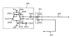
SDRAM1000は、さらに、各メモリセルプレーンM♯0〜M♯3に対応して設けられ、外部から与えられる行アドレス信号Xaに応じて、対応するメモリプレーンの行を選択する行デコーダ106と、メモリプレーンM♯0〜M♯3に対応して設けられ、内部からの列アドレス信号Ybに応じて、対応するメモリプレーンの列を選択する列デコーダ108と、読出動作において、選択されたメモリセルからのデータの読出を行ない、書込動作において選択されたメモリセルに対してデータの書込を行なう入出力回路110と、外部から与えられる制御信号ext.CKE、ext./CS、ext./RAS、ext./CASおよびext./WEに応じて、各内部回路の動作を制御し、たとえばセルフリフレッシュモードにおいては、活性なセルフリフレッシュモード指定信号/REFSを出力し、後に説明するように、データ出力動作を制御する信号/CACTを活性状態(“L”レベル)とする制御回路100と、外部クロック信号ext.CLKが与えられる外部クロック入力パッド112と、外部クロック入力パッドからの外部クロック信号ext.CLKを受けて、バッファ処理して出力する第1の入力初段バッファ回路202と、入力初段バッファ回路202の出力を受けて、第1の内部クロック信号int.CLK1を出力する第1のクロック発生回路102と、外部クロック入力パッド112からの外部クロック信号を受けて、バッファ処理して出力する第2の入力初段バッファ回路200と、入力初段バッファ回路200の出力を受けて、データ出力動作を制御する第2の内部クロック信号int.CLK2を出力する第2のクロック発生回路204と、メモリプレーンM♯0から読出されたデータを受けて、第2の内部クロック信号CLK2に制御されてデータ入出力パッド114を駆動する出力バッファ回路118と、第2のクロック発生回路とチップ左側に存在するデータ入出力パッドDQLに対応する出力バッファ118との間を接続する配線206と、チップ左側に存在するデータ入出力パッドDQRに対応する出力バッファ回路118と第2のクロック発生回路204との間を接続する配線208とを含む。
【0071】
なお、図1においては、メモリセルプレーンM♯0〜M♯3は4つ存在し、パッドと周辺回路の両者をチップの真ん中に十字形形状に配置することができるように、所定の余裕領域を残して配置されている構成としたが、以下の説明で明らかとなるように、本発明はこのような構成に限定されることなく、より一般的なメモリセルプレーンの個数および配置に対して適用することが可能である。たとえば、メモリセルプレーンは2つ存在し、パッドと周辺回路の両者をチップの真ん中に一文字形状に配置することができるように、所定の余裕領域を残して配置されている構成とすることも可能である。
【0072】
ここで、第1のクロック発生回路102から出力される内部クロック信号int.CLK1は、SDRAM1000のロウ系回路、たとえば行デコーダ106等の動作や、コラム系回路、たとえば列デコーダ108や入出力回路110等の動作の制御に用いられる。
【0073】
また、第1の入力初段回路202の動作は、信号/REFSが活性状態(“L”レベル)である期間は不活性状態となるものとする。
【0074】
一方、第2の入力初段バッファ回路200の動作は、後に説明するように信号/CACTにより制御され、読出動作期間中においてのみ活性状態となるものとする。
【0075】
ここで、信号/REFSや、信号/CACTが、活性状態となるかあるいは不活性状態となるかは、後に説明するように、制御回路100に与えられる外部からの制御信号の組合せによって規定されるものとする。
【0076】
図1に示したSDRAM1000の構成が、図21に示した従来のSDRAM4000の構成と異なる点は、以下のとおりである。
【0077】
まず第1に、外部クロック信号ext.CLKが与えられる外部クロック入力パッド112に接続する入力初段バッファ回路は、第1の入力初段バッファ回路202および第2の入力初段バッファ回路200の2つに分けられ、第1の入力初段バッファ回路202は、上述のとおり、ロウ系あるいはコラム系またはさらに他の内部回路等を制御するための内部クロック信号を発生する第1のクロック発生回路102に対して、外部クロック信号を伝達する。これに対して、第2の入力初段バッファ回路200は、出力バッファ回路118の動作を制御する内部クロック信号を出力する第2のクロック発生回路204に対して外部クロック信号ext.CLKを伝達する。
【0078】
第2には、上記第2の入力初段バッファ回路200は、第1の入力初段バッファ回路202に比べて、電流駆動能力が大きくなるように構成されている点である。すなわち、第2の入力初段バッファ回路200を構成するトランジスタのトランジスタサイズは、第1の入力初段バッファ回路202を構成するトランジスタのトランジスタサイズに比べて大きくなるように設定されている。
【0079】
第3には、第1の入力初段バッファ回路202は、信号/REFSに制御されて、リフレッシュ期間中以外は活性状態となる構成となっており、第2の入力初段バッファ回路200は、信号/CACTに制御されて、読出動作期間中においてのみ活性状態となる構成となっている点である。
【0080】
第4には、第2のクロック発生回路204から出力される信号をパッドDQLに対応する出力バッファ118に対して伝達する配線206は、一度チップ中央部まで延びた後、折返されて、出力バッファ118に到達するように形成されている点である。
【0081】
図2は、図1に示したSDRAM1000の構成のうち、外部クロック入力パッド112、第2の入力初段バッファ回路200、第2のクロック発生回路204、出力バッファ118へ内部クロック信号を伝達する配線206および208の部分を抽出して示す概略ブロック図である。
【0082】
上述したとおり、配線206は、一旦配線208と同一方向に延在した後、折返されて、配線208とは反対方向に向かうように形成されている。
【0083】
図3は、図2に示した第2の入力初段バッファ回路200および第2のクロック発生回路204の構成をより詳細に示すブロック図である。
【0084】
第2の入力初段バッファ回路200は、ともにソースに電源電位Vccを受け、カレントミラー回路を構成するpチャネルMOSトランジスタ対2002および2004と、pチャネルMOSトランジスタ2002のドレインとドレインが接続し、ゲートに基準電位Vrefを受けるnチャネルMOSトランジスタ2008と、pチャネルMOSトランジスタ2004のドレインとドレインが接続し、ゲートに外部クロック信号ext.CLKを受けるnチャネルMOSトランジスタ2010と、ソースが接地電位GNDと接続し、ドレインが、nチャネルMOSトランジスタ2008および2010のソースと共通に接続し、ゲートに信号/CACTがインバータ2014によって反転された信号を受けるnチャネルMOSトランジスタ2012と、ゲートに、インバータ2014の出力を受け、pチャネルMOSトランジスタ2004と並列に接続されるpチャネルMOSトランジスタ2006と、pチャネルMOSトランジスタ2004およびnチャネルMOSトランジスタ2010の接続点の電位を受け、外部に反転して出力するドライバ回路2016とを含む。
【0085】
一方、第2のクロック発生回路204は、ドライバ回路2016の出力を受けて、配線208に対して、内部クロック信号を出力するドライバ回路として動作するインバータ2042と、ドライバ回路2016の出力を受けて、配線206に対して、内部クロック信号int.CLKを出力するドライバ回路として動作するインバータ2044とを含む。
【0086】
なお、第1の入力初段バッファ回路202の構成も、制御信号が信号/REFSとなっている点を除いては、基本的に第2の入力初段バッファ回路200の構成と同様である。
【0087】
図3に示した本発明の実施の形態1の第2の入力初段バッファ回路および第2のクロック発生回路の構成を、図23に示した従来の入力初段バッファ回路およびクロック発生回路の構成と比較すると、以下の有利な点が存在する。
【0088】
すなわち、第1には、第2の入力初段バッファ回路200は、信号/CACTにより制御されて、信号/CACTが活性である期間、すなわち読出動作モードが指定されている期間のみ活性状態となるため、第2の入力初段バッファ回路200を構成するトランジスタサイズ等を大きくした場合でも、スタンバイ状態におけるSDRAM1000の動作電流を増大させるということがない。
【0089】
言い換えると、 第1の入力初段バッファ回路と第2の入力初段バッファ回路とを独立して構成しているので、データ出力動作のクリティカルパスであって、大きな電流駆動能力が要求される第2の入力初段回路200等に十分な電流駆動能力を有するような設計を行なった場合でも、第2の入力初段バッファ回路は、読出期間のみしか動作しないため、SDRAM1000の待機動作中の動作電流が増大するということがない。
【0090】
さらに、第2のクロック発生回路204は、第2の入力初段バッファ回路200の近傍に隣接して設けられるため、ドライバ回路2016は、大きな配線容量を駆動する必要がなく、しかも、ドライバ回路2016は、配線206および208を駆動するインバータ2042および2044のみを駆動すればよいため、このドライバ回路2016の電流駆動能力等に対する設計の自由度を広げることができる。
【0091】
また、上述したとおり、配線206は、チップ中央部近傍まで配線208と同一方向に走った後、配線208とは逆転した方向に走り、出力バッファ回路118と接続される構成となっているので、配線206の総配線長を適当な値に設定することで、第2のクロック発生回路204から出力された内部クロック信号int.CLK2がチップ両端に存在する出力バッファ回路118にそれぞれ到達する時間の時間差を抑制するように構成することが可能である。
【0092】
このため、データ出力時に生じる出力データのスキュー等が低減され、より速いサイクルタイムに対応して動作させることが可能となる。
【0093】
図4は、図1に示したSDRAM1000の動作を説明するためのタイミングチャートである。
【0094】
時刻t0〜時刻t1の期間において、信号ext.CKEが活性状態(“L”レベル)へと変化する。
【0095】
時刻t1における外部クロック信号ext.CLKの立上がりのエッジにおいて、信号ext.CKE、信号ext./CS、ext.RAS、およびext./CASがすべて活性状態(“L”レベル)であり、かつ信号ext./WEが非活性状態(“H”レベル)であることに応じて、制御回路100は、セルフリフレッシュモードが指定されたことを検知して、信号/REFSを活性状態(“L”レベル)とする。
【0096】
このとき、図1において説明したとおり、第1の入力初段バッファ回路202は、信号/REFSが活性状態となるのに応じて、非活性状態となる。
【0097】
一方、信号/CACTは、非活性状態の(“H”レベル)であるため、第2の入力初段バッファ回路200も非活性状態である。
【0098】
セルフリフレッシュモードにおいては、制御回路100から出力される内部アドレス信号に応じて、メモリプレーンM♯0〜M♯3中の各行が順次選択され、データの再書込動作、すなわちリフレッシュ動作が行なわれることになる。
【0099】
時刻t3〜時刻t4の期間において、信号ext.CKEが非活性状態(“H”レベル)へと変化する。
【0100】
したがって、時刻t4における外部クロック信号ext.CLKの立上がりのエッジにおいて、制御信号ext.CKE、ext./CS、ext./RAS、ext./CASおよびext./WEが非活性状態(“H”レベル)であることに応じて、制御回路100は、セルフリフレッシュモードの終了が指定されたことを検出して、セルフリフレッシュ動作を終了する。
【0101】
時刻t6における外部クロック信号ext.CLKの立上がりのエッジにおいて、信号ext./CSおよびext./RASがともに活性状態(“L”レベル)であって、信号ext.CKE、ext./CASおよびext./WEが不活性状態(“H”レベル)であることに応じて、制御回路100は、この時点において、外部アドレス入力端子(パッド)に与えられている信号を行アドレス信号として取込むように制御する。
【0102】
この時点においては、信号/REFSは非活性状態(“H”レベル)であって、第1の入力初段バッファ回路202は動作しており、それに応じて、第1のクロック発生回路102も動作して、内部クロック信号int.CLK1を対応する内部回路に供給している。
【0103】
時刻t8における外部クロック信号ext.CLKの立上がりのエッジにおいて、制御信号ext./CSおよびext./CASがともに活性状態であって、信号ext.CKE、ext./RAS、およびext./WEがすべて非活性状態であることに応じて、制御回路100は、この時点でアドレス信号入力端子(パッド)に与えられている信号を、列アドレス信号として取込むように指示する。
【0104】
図4に示した場合においては、CASレイテンシー、すなわち、このようにして、列アドレス信号が取込まれるサイクルから、データ出力が開始されるまでのサイクル数CLが2であるように指定されているものとする。
【0105】
このような指定は、たとえば、読出動作のセットサイクル(図示せず)において、制御信号と、アドレス信号との組合せによって指定されているものとする。
【0106】
信号ext./CSおよびext./CASがともに活性状態であることに応じて、制御回路100は、信号/CACTを活性状態(“L”レベル)へと変化させる。これに応じて、図3において説明したとおり、第2の入力初段バッファ回路200は活性状態へと変化する。
【0107】
したがって、第2のクロック発生回路204から、出力バッファ回路118に対して、第2の内部クロック信号int.CLK2の供給が開始されることになる。
【0108】
時刻t8から2サイクル経過した後の時刻t10において、選択されたメモリセルから読出されたデータの出力動作が開始される。
【0109】
本実施の形態においては、1回の読出動作において、1つのデータ入出力端子(パッド)当り出力されるデータ数、すなわちバースト長BLは2が指定されているものとする。
【0110】
このバースト長の指定も、読出動作モードのセットサイクル(図示せず)における、制御信号の組合せおよびアドレス信号の組合せによって指定されているものとする。
【0111】
時刻t10において、1ビット目の読出データが出力された後、時刻t11において2ビット目のデータの出力が行なわれる。このとき、同時に、時刻t11において、制御信号ext./CS、ext./RAS、ext./WEがすべて活性状態であって、信号ext.CKEおよび信号ext./CASが不活性状態であることに応じて、読出動作の終了が指定され、これに応じて制御回路100は、時刻t12において、信号/CACTを非活性状態(“H”レベル)へと変化させる。
【0112】
以上の動作において説明したとおり、実施の形態1のSDRAM1000においては、リフレッシュ動作期間中においては、第1および第2の入力初段バッファ回路202および200は、ともに非活性状態であるため、この期間中において、差動増幅器による貫通電流による消費電流の増加が抑制される。
【0113】
さらに、第2の入力初段バッファ回路200の電流駆動能力を大きくするために、それを構成するトランジスタのトランジスタサイズを大きくした場合でも、第2の入力初段バッファ回路は、読出動作モード期間中のみ活性状態とされるため、スタンバイ状態における消費電流が増大するということがない。
【0114】
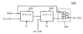
図5は、図4に示したように、読出動作期間中のみ信号CACTを活性状態とするために制御回路100に含まれる部分回路1100を示す図である。
【0115】
図6は、図5に示した回路からの出力を受けて、所定のサイクル数の期間のみ信号/CACTを活性状態とするための制御回路100中の部分回路1200の構成を示す概略ブロック図である。
【0116】
図5を参照して、回路1100は、信号ext./RASの反転信号である信号RAS、信号ext./CAS、信号ext./CSおよび信号ext./WWEの反転信号である信号WEを受ける4入力NAND回路1002と、NAND回路1002の出力を受け、内部クロック信号int.CLK1およびその反転信号int./CLK1に制御されて、信号READを出力するクロックドインバータ回路1104とを含む。
【0117】
図6を参照して、回路1200は、CASレイテンシーCLおよび内部クロック信号int.CLK1を受けて、信号READの活性化に応じて、計数動作を開始し、計数した外部クロック信号int.CLK1のサイクル数がCASレイテンシーCLと一致することに応じて、出力信号のレベルを活性状態とするカウンタ1202と、カウンタ1202の出力の信号レベルの活性化に応じて計数動作を開始して、内部クロック信号int.CLK1のサイクル数を計数し、バースト長BLと一致した時点で、出力信号レベルを活性状態とするカウンタ1204と、信号READの活性化に応じて、信号/CACTを活性状態とし、カウンタ1204の出力信号の活性化に応じて、信号/CACTを不活性状態とするラッチ回路1206とを含む。
【0118】
図5および図6に示した回路1100および1200の構成によって、図4に示したような信号/CACTを生成することが可能となる。
【0119】
[実施の形態2]
実施の形態1におけるSDRAM1000においては、第2の入力初段回路200は、読出動作モードにおいてのみ活性状態となる構成であった。
【0120】
実施の形態2のSDRAMにおいては、第2の入力初段バッファ回路200は、SDRAM1000がアクティブ状態、すなわち、ロウ系の回路の動作が活性状態となった後、読出動作が終了して、ロウ系回路等のプリチャージ動作が開始されるまでの期間において、第2の入力初段バッファ回路200が活性となる構成となっている。
【0121】
その他の点は図1に示したSDRAM1000の構成と同様であるので、説明は繰返さない。
【0122】
図7は、制御回路100中に含まれ、第2の入力初段バッファ回路200の動作を制御するための制御信号/CACTを発生する初段バッファ制御回路の第1の部分回路1300を示す図であり、図8は、初段バッファ制御回路の第2の部分回路1400の構成を示す概略ブロック図である。
【0123】
第1の部分回路1300は、信号ext./RAS、信号ext./CASの反転信号の信号/CAS、信号ext./CS、信号ext./WEの反転信号の信号WEを受ける4入力NAND回路1302と、NAND回路1302の出力を受けて、信号int.CLK1およびその反転信号であるint./CLK1に制御されて、信号ACTを出力するクロックドインバータ回路1304と、信号ext./RAS、信号CAS、信号ext./CSおよび信号ext./WEを受ける4入力NAND回路1306と、NAND回路1306の出力を受けて、信号int.CLK1、int./CLK1に制御されて、信号PRCを出力するクロックドインバータ回路1308とを含む。
【0124】
図8を参照して、第2の部分回路1400は、信号PRCの反転信号と信号ACTとを受けるNOR回路1402と、信号PRCと、信号ACTの判定信号とを受けるNOR回路1404と、NOR回路1406および1408を交差接続させて構成させるSRフリップフロップ回路1410とを含む。
【0125】
ここで、NOR回路1402の出力は、SRフリップフロップ回路1410のリセット信号として入力し、NOR回路1404の出力は、SRフリップフロップ回路のセット信号Sとして入力する。SRフリップフロップ回路1410の反転出力が、信号/CACTとして出力される。
【0126】
図9は、本発明の実施の形態2のSDRAMの動作を説明するためのタイミングチャートである。
【0127】
図4に示した実施の形態1のSDRAM1000の動作と異なる点は、以下のとおりである。
【0128】
すなわち、本実施の形態においては、時刻t1において、信号ext./CSおよび信号ext./RASが活性状態となって、行アドレス信号が取込まれた後、時刻t3において、信号ext./CSおよび信号ext./CASが活性状態となって、列アドレス信号が取込まれると、時刻t5において、データの出力が開始される点では、実施の形態1のSDRAM1000の動作と同様である。
【0129】
しかしながら、バースト長BLが2であって、時刻t6において、2ビット目の読出データDQ2が出力される時点においては、信号ext./CS、ext./RAS、およびext./WEは活性状態とならず、プリチャージ状態の指定は行なわれない。続いて、時刻t13において、再びデータの読出が行なわれ、バースト長で指定されたデータ分だけデータの出力が行なわれる時刻t14において、信号ext./CS、ext./RASおよびext./WEが活性状態となって、ロウ系回路のプリチャージ動作の指定が行なわれる。
【0130】
すなわち、図9に示した実施の形態2のSDRAMの動作においては、時刻t1において、ロウ系の回路の活性化が指示された後、時刻t14において、プリチャージ動作が指定されて、ロウ系の回路のプリチャージ動作が指示されるまでの期間は、その間に2回ないしはそれ以上の回数の読出動作が存在する場合においても、信号/CACTは活性状態を維持する。
【0131】
これに対して、実施の形態1のSDRAM1000においては、リード動作が終了するたびにプリチャージ動作が開始されてしまうため、引続いて読出動作を行なう場合には、このプリチャージ動作が完了するまでの期間だけ余分に時間が必要となる。
【0132】
つまり、実施の形態2のSDRAMは、連続して読出モードが指定されるような場合において、より高速な動作を行なうことが可能である。
【0133】
[実施の形態3]
図10は、本発明の実施の形態3のSDRAM2000の構成を示す概略ブロック図である。
【0134】
図1に示した実施の形態1のSDRAM1000の構成と異なる点は、以下のとおりである。
【0135】
第1には、各メモリセルプレーンM♯0〜M♯3が各々4つのメモリセルブロックMB0〜MB3に分割されている点である。
【0136】
さらに、各メモリセルブロックMB0〜MB3ごとに対応して、行デコーダ106a〜106dがそれぞれ設けられ、各メモリセルブロックに対応して、それぞれ列デコーダ108a〜108dおよび入出力回路110a〜110dが設けられている。
【0137】
ここで、図10においては、列デコーダおよび入出力回路を1つのブロックで示している。
【0138】
さらに、メモリセルブロックの対MB0およびMB1ならびにもう1つのメモリセルブロックの対MB2およびMB3ごとに、ローカルクロック発生回路300および302が設けられる構成となっている。つまり、第2のクロック発生回路204の出力の内部クロック信号は、出力バッファ118にではなく、ローカルクロック発生回路300および302に対して与えられる構成となっている。これに応じて、ローカルクロック発生回路300および302は、対応するメモリセルブロックに対して、内部クロック信号を供給する。
【0139】
また、入出力回路110から出力されたデータは、一旦各メモリセルブロックに対応して設けられているバスドライバ回路304a〜304dにおいてその値が保持される構成となっている。さらに、選択されたメモリセルに応じて、バスドライバ回路304a〜304dのいずれかから出力される読出データは、バスドライバ回路304a〜304dに対して共通に接続する中間ラッチ回路306において再び保持される構成となっている。
【0140】
中間バッファ回路306は、保持している読出データを、出力バッファ118に対して与える構成となっている。
【0141】
なお、図10においては、メモリプレーンM♯2およびM♯3に対応する構成のみを示したが、同様の構成が、メモリプレーンM♯0およびM♯1に対応しても存在している。
【0142】
なお、図10においては、出力バッファ118には、図示を容易とするため、メモリセルプレーンM♯2およびM♯3からの読み出しデータが与えられる構成としているが、図1の構成と本質的に相違するわけではない。
【0143】
その他、図1に示した実施の形態1のSDRAM1000と同一部分には同一参照符号を付してその説明は繰返さない。
【0144】
図11は、図10に示したSDRAM2000の構成において、図示されていなかった外部アドレス入力パッドおよび列アドレスバッファを含めて、メモリセルブロックから、出力バッファまでの信号の流れを示すための模式図である。
【0145】
以下では、外部から与えられた行アドレス信号に応じて、1本のワード線WLが既に選択されているものとする。
【0146】
続いて、外部アドレス入力パッド310に与えられる列アドレス信号Ybを受けて、列アドレスバッファ312は、プリデコーダ314に対して、列アドレス信号を出力する。
【0147】
ここで、プリデコーダ314中にはラッチ回路が含まれ、列アドレスバッファ312から出力される列アドレス信号は、図10に示した第1のクロック発生回路102からの内部クロック信号int.CLK1の活性化に応じて、アドレスバッファ312からのデータのラッチ動作を行なう。
【0148】
続いて、プリデコーダ314において選択されたメモリセルブロックに対して、対応する列アドレス信号が与えられる。これに応じて、列デコーダ108は、対応する列の選択を行なう。
【0149】
すなわち、選択されたワード線WLに接続するメモリセルMC中の記憶データに応じて、センスアンプ316は、対応するビット線対BLおよび/BLの電位差を増幅する。このセンスアンプ316によって増幅された電位レベルは、列デコーダ108により制御されるトランスファーゲート320を介して、ローカルIO線対(図示せず)に伝達された後、グローバルIO線対GI/Oおよび/GI/Oへと伝達される。
【0150】
グローバルIO線対GI/Oおよび/GI/Oまで読出された記憶データは、プリアンプ318により増幅され、バスドライバ304に伝達される。バスドライバ304中には、後に説明するようにラッチ回路が含まれており、このバスドライバ304中のラッチ回路は、ローカルクロック発生回路300または302から出力される内部クロック信号int.CLKLにより制御される。
【0151】
続いて、バスドライバ320により駆動されるデータバスの出力に応じて、中間バッファ306は、内部クロック信号int.CLKLに応じて動作するラッチ回路によりそのデータを保持して、かつ出力する。
【0152】
中間バッファ306からの出力を受けて、出力バッファ118は、第1のクロック発生回路からの内部クロック信号int.CLK1に応じて、データを保持し、かつ対応するデータ入出力パッド114の電位レベルを、読出データに応じて駆動する。
【0153】
すなわち、実施の形態3のSDRAM2000においては、メモリセルブロックから読出され、プリアンプにより増幅された読出データの、バスドライバ304におけるデータラッチ動作および中間バッファ306のデータラッチ動作は、ローカルクロック発生回路300または302からの内部クロック信号int.CLKLにより制御される構成となっている。
【0154】
図12は、図11に示したバスドライバ回路304、中間バッファ306、および出力バッファ回路118の構成を示すブロック図である。
【0155】
以下では、バスドライバ304の構成として説明するが、中間バッファまたは出力バッファにおいても、その制御される内部クロック信号が異なるのみで、その基本的な構成は全く同様である。
【0156】
バスドライバ304は、クロック信号CLKLが“L”レベルにおいて導通状態となるトランスミッションゲート3042と、トランスミッションゲート3042の出力を受けて保持するラッチ回路3044と、ラッチ回路3044の出力を受けて、反転するインバータ3046と、インバータ3046の出力を受けて、内部クロック信号int.CLKLが“H”レベルにおいて導通状態となるトランスミッションゲート3048と、トランスミッションゲート3048の出力を受けて、保持するラッチ回路3050と、ラッチ回路3050の出力を受けて、反転して出力するインバータ3052とを含む。
【0157】
つまり、ラッチ回路3050およびインバータ3052で、出力側を駆動するドライバ回路が構成される。
【0158】
図12に示したその構成から明らかなように、バスドライバ304は、内部クロック信号int.CLKLが“L”レベルにある状態において、データの取込を行ない、そのデータを、クロック信号int.CLKLが“H”レベルとなった時点で、ラッチ回路3050に伝達し、そのデータを外部に出力する構成となっている。
【0159】
図13は、図10および図11に示したSDRAM2000の動作を説明するためのタイミングチャートである。
【0160】
時刻t1において、信号ext./CSおよびext./RASが活性状態となるのに応じて、行アドレス信号が取込まれ、時刻t3において、信号ext./CSおよび信号ext./CASが活性状態となることで、列アドレス信号の取込が行なわれることは、実施の形態1のSDRAM1000と同様である。
【0161】
なお、本実施の形態においては、時刻t1において、ロウ系の回路が活性となるのに応じて、第2の入力初段バッファ回路200の動作を活性化する信号/CACTが活性状態(“L”レベル)となるものとする。
【0162】
ただし、図4に示したように、読出動作においてのみこの信号/CACTが活性状態となる構成とすることも可能である。
【0163】
図13に示した構成においては、CASレイテンシーCLは4に設定されているものとする。
【0164】
したがって、時刻t3から4サイクル後の時刻t7においてデータの出力が開始されることになる。
【0165】
以下では、図11を参照して、信号ext./CASが活性状態となって、列アドレス信号Ybが取込まれる時刻t3から、データ出力が開始される時刻t7までの動作についてより詳しく説明することにする。
【0166】
時刻t3において、列アドレス信号が取込まれる時点では、第1のクロック発生回路102からの内部クロック信号int.CLK1に応じて、プリデコーダ314における列アドレス信号のラッチ動作およびプリデコード動作が行なわれる。
【0167】
プリデコーダ314から出力される内部列アドレス信号に応じて、列デコーダ108が対応する列の選択を行ない、グローバルIO線対GI/Oおよび/GI/Oに読出データが伝達され、プリアンプ318により増幅動作が行なわれる。
【0168】
時刻t4においては、プリアンプ318により増幅された読出データは、内部クロック信号int.CLKLにより制御されるパスドライバ304においてラッチされ、対応するデータがデータバスに出力される。
続いて時刻t5において、データバス上の読出データは、中間バッファ306において、内部クロック信号int.CLKLに同期してラッチされ、出力バッファ118に対して出力される。
【0169】
時刻t6において、出力バッファ118は、第1のクロック発生回路からの内部クロック信号int.CLK1に応じて、中間バッファ306からのデータをラッチし、かつデータ入出力パッド114に対して、読出データの出力を行なう。
【0170】
すなわち、実施の形態3のSDRAM1000においては、プリアンプで増幅後、出力バッファ回路にデータが伝送されるまでの、SDRAMのパイプライン動作におけるデータラッチ動作が、ローカルクロック発生回路300または302から出力される内部クロック信号int.CLKLにより制御される構成となっている。
【0171】
このため、実施の形態1のSDRAM1000においては、外部クロック信号が、第1の入力初段バッファ回路202によりバッファ処理された後、第1のクロック発生回路102により発生される内部クロック信号int.CLK1において、上記一連の動作が同期して制御される構成となっていた。このため、これらの動作の高速化を図るためには、第1の入力初段バッファ回路および第1のクロック発生回路102の駆動能力を増大させることが必要で、これらの回路を構成するトランジスタサイズを大きくしたり、あるいはバッファを構成するインバータ等の段数を増加させる必要があった。
【0172】
これに対して、実施の形態2のSDRAM2000においては、図13に示した第2ステージ(プリアンプ318からの読出データをバスドライバがラッチするサイクル)および第3ステージ(バスドライバ304からの読出データを中間バッファ306が保持するサイクル)の動作が、独立したローカルクロック発生回路300または302からの出力の内部クロック信号int.CLKLにより制御される構成となっているので、チップ中央部から、ローカルのクロック発生回路までの配線長が、メモリ容量の大容量化とともに長くなり、この配線の時定数が読出動作のクリティカルパスとなった場合でも、この配線の電位を駆動する駆動回路の段数の削減や、内部クロック信号のスキューの発生等を緩和することで、低消費電力でかつ高速な動作を図ることが可能となる。
【0173】
図14は、実施の形態3のSDRAM2000の変形例のSDRAM3000の構成を示す概略ブロック図である。
【0174】
図10に示した実施の形態3のSDRAM2000の構成と異なる点は、出力バッファ回路118が、第2のクロック発生回路204からの内部クロック信号int.CLK2により制御される構成となっている点である。
【0175】
その他の点は、図10に示した実施の形態3のSDRAM2000の構成と同様であるので、同一部分には同一符号を付してその説明は繰返さない。
【0176】
実施の形態3のSDRAM3000においては、出力バッファ回路118が、第2のクロック発生回路204から出力される内部クロック信号int.CLK2により制御される構成となっているので、実施の形態1において説明したとおり、出力バッファ回路が、チップ中央部から離れたチップ端部に位置している場合でも、外部クロック信号に応じて発生される内部クロック信号の伝達に要する遅延時間を低減でき、動作可能なクロック周波数を増加させることが可能となる。
【0177】
さらには、このような構成とした場合においても、第2のクロック発生回路204に対して、外部クロック信号を伝達する入力初段バッファ回路200は、信号/CACTにより制御され、SDRAM3000のデータ読出モード期間中または、アクティブ期間中においてのみ動作する構成となっているので、高速なアクセスを可能とするために、それを構成するトランジスタサイズ等を増加させた場合でも、スタンバイ状態における消費電力の増大を抑制することが可能となる。
【0178】
[実施の形態4]
実施の形態のSDRAMの基本的な構成は、以下に説明する点を除いて、図1に示したSDRAM1000の構成と同様である。
【0179】
すなわち、実施の形態4のSDRAMにおいては、実施の形態1のSDRAM1000の構成において、第2のクロック発生回路204から出力バッファ回路118に対して、内部クロック信号int.CLK2を伝達する配線206または208の配線幅または隣接する配線との配線間距離とをより高速動作に適した構成としている。
【0180】
図15は、配線206または208と隣接する他の配線との関係を模式的に示す図である。
【0181】
ここで、配線幅をL、配線間距離をSで表わすこととする。
図16は、配線ピッチ、すなわち配線幅Lと配線間距離Sとの和に対する、配線遅延時間と、配線面積との関係を示すグラフである。
【0182】
ここでは、配線幅Lと配線間距離Sとの比を1に固定した場合について示している。
【0183】
配線幅に対する配線間距離が一定値に保持されている場合、配線遅延は、ピッチの増加に伴い、初期的には減少していく。これは、配線幅の増大に伴って、配線抵抗が減少するためである。
【0184】
ただし、配線ピッチが4μmを超えると、逆に配線遅延量は増大していく。これは、配線幅が増大したことにより、対地容量が増大し、逆に配線遅延量が増加していくためである。
【0185】
すなわち、配線遅延には、配線幅と配線間距離を一定とした場合、最適値が存在することになる。
【0186】
しかしながら、配線遅延の大きさのみから、配線幅を決定するのは、配線面積の観点からすると妥当ではない。
【0187】
つまり、配線ピッチが増大するにつれて、配線面積は一様に増加していくため、単純は配線遅延の最適点が、チップ面積等も考慮した場合の最適点であるとは限らない。
【0188】
そこで、逆にチップ面積等も考慮して、配線遅延を決定することとすると、L/S=1μm/1μm程度が最適点となる。
【0189】
このため、チップ内部の信号線は、ほとんどこのピッチでレイアウトされている。しかしながら、クロック信号を伝達する配線は、高速性が要求されるため、配線ピッチを最適点に設定するとすると、図16に示すとおり、L/S=2μ/2μが最適となる。
【0190】
L/Sの比が1である場合、上述のとおり、L/S=2μ/2μ程度が最適となるが、L/S<1にすれば、配線遅延はさらに小さくすることが可能となる。
【0191】
また、配線幅Lおよび配線間距離Sの最適点は、配線の厚み、配線周りの絶縁膜の誘電率等によっても変化する。
【0192】
したがって、クロック配線に対する配線幅Lまたは配線間距離Sは、その周りに使用されている配線の配線幅もしくは配線間間隔よりも大きくすることが必要であって、クロック配線の配線幅または配線間距離は、周囲の配線に比べて1.5倍以上の値とすることが必要である。
【0193】
このような値とすることで、他の信号配線よりも高速動作が要求されるクロック信号配線の配線遅延を、チップ全体として見た場合に最適化することが可能となる。
【0194】
【発明の効果】
請求項1記載の同期型ダイナミック型半導体記憶装置は、出力バッファ回路を駆動するための内部クロック信号を発生するクロック発生手段を、独立した構成としたので、出力バッファ回路への内部クロック信号の伝達が、データ読出動作において、クリティカルパスとなる場合であっても、その動作速度を向上させることが可能である。さらに、出力バッファ回路を制御するための第2の内部クロック信号を発生する第2のクロック発生手段に外部クロック信号を伝達する第2のクロック入力バッファ手段の電流駆動能力を、他の内部回路を駆動するための第1の内部クロックを発生する第1のクロック発生手段に対する第1のクロック入力バッファ手段よりも大きくする構成としたので、出力バッファへのクロック信号の伝達が動作速度のクリティカルパスとなる場合でも、その動作速度を高速化することが可能である。
請求項2記載の同期型ダイナミック型半導体記憶装置は、制御手段や、第1および第2のクロック発生手段が、偶数個のメモリセルプレーンの配置されていないチップ中央の余流領域に配置される構成となっているので、チップの行および列のいずれの方向から見ても、各メモリセルプレーンに対する制御手段等からの配線長が最短となるように配置することが可能で、配線遅延によるアクセス時間の増大を抑制することができる。さらに、データ出力手段への内部クロック信号は、独立した第2のクロック発生手段により供給されるので、データ出力手段への内部クロック信号の伝達遅延を抑制することが可能で、アクセス時間の増大を抑制することが可能である。さらに、出力バッファ回路を制御するための第2の内部クロック信号を発生する第2のクロック発生手段に外部クロック信号を伝達する第2のクロック入力バッファ手段の電流駆動能力を、他の内部回路を駆動するための第1の内部クロックを発生する第1のクロック発生手段に対する第1のクロック入力バッファ手段よりも大きくする構成としたので、出力バッファへのクロック信号の伝達が動作速度のクリティカルパスとなる場合でも、その動作速度を高速化することが可能である。
【0196】
請求項3記載の同期型ダイナミック型半導体記憶装置は、請求項1または2記載の同期型ダイナミック型半導体記憶装置の構成において、出力バッファ回路を制御するための第2の内部クロック信号を発生する第2のクロック発生手段およびそれに近接し外部クロック信号を伝達する第2のクロック入力バッファ手段を、他の内部回路を駆動するための第1の内部クロックを発生する第1のクロック発生手段および第1のクロック入力バッファ手段とは別系統としたので、出力バッファへのクロック信号の伝達が動作速度のクリティカルパスとなる場合でも、その動作速度を高速化するための設計の自由度が向上する。
【0197】
請求項4記載の同期型ダイナミック型半導体記憶装置は、請求項3記載の同期型ダイナミック型半導体記憶装置の構成において、第2のクロック入力バッファ手段は、データ読出モード中において活性状態となる構成としたので、スタンバイ状態における消費電力の増大を抑制することが可能である。
【0198】
請求項5記載の同期型ダイナミック型半導体記憶装置は、請求項3記載の同期型ダイナミック型半導体記憶装置の構成に加えて、第1のクロック入力バッファ手段は、セルフリフレッシュモード期間中は非活性状態となるので、スタンバイ期間中の消費電力の増加を抑制することが可能となる。
【0199】
請求項6記載の同期型ダイナミック型半導体記憶装置は、請求項3記載の同期型ダイナミック型半導体記憶装置の構成に加えて、第2のクロック発生手段から、チップ端部に存在する出力バッファに対して第2の内部クロック信号を伝達する配線の配線幅が、それに隣接する他の配線幅よりも大きな構成としたので、第2の内部クロック信号の伝達を行なう配線の配線遅延を抑制することが可能である。
【0200】
請求項7記載の同期型ダイナミック型半導体記憶装置は、請求項3記載の同期型ダイナミック型半導体記憶装置の構成において、第2のクロック発生手段から、チップ端部に存在する出力バッファ回路へ第2の内部クロック信号を伝達する配線の配線間隔が、他の配線の配線間隔よりも大きくする構成としたので、出力バッファ回路に対して、第2の内部クロック信号を伝達する配線の配線遅延を抑制することが可能である。
【0201】
請求項8記載の同期型ダイナミック型半導体記憶装置は、メモリセルから読出された読出データのラッチ動作のタイミングが、独立に設けられた第2のクロック発生手段からの第2の内部クロックによって制御される構成となっているので、メモリ容量の大容量化とともに、第2の内部クロック信号を伝達する配線長が長くなった場合でも、読出動作におけるアクセス時間の増大を抑制することが可能である。
請求項9記載の同期型ダイナミック型半導体記憶装置は、第2のクロック発生手段から、チップの両端部に存在する出力バッファ回路へ第2の内部クロック信号を伝達する配線の配線長が、チップの両側に対して同一となるように構成することが可能で、第2の内部クロック信号のスキューを抑制することが可能である。
【0210】
請求項10記載の同期型ダイナミック型半導体記憶装置は、第2のクロック発生手段から、チップの両端部に存在する出力バッファ回路へ第2の内部クロック信号を伝達する配線の配線長が、チップの両側に対して同一となるように構成することが可能で、第2の内部クロック信号のスキューを抑制することが可能である。
【図面の簡単な説明】
【図1】 本発明の実施の形態1のSDRAM1000の構成を示す概略ブロック図である。
【図2】 SDRAM1000の内部クロック発生の主要部を示すブロック図である。
【図3】 図2に示した内部クロック発生の主要部の構成をさらに詳しく示す概略ブロック図である。
【図4】 SDRAM1000の動作を説明するためのタイミングチャートである。
【図5】 制御回路100中に含まれる第1の部分回路1100の構成を示す概略ブロック図である。
【図6】 制御回路100中に含まれる第2の部分回路1200の構成を示す概略ブロック図である。
【図7】 本発明の実施の形態2のSDRAMの制御回路100中に含まれる第1の部分回路1300の構成を示す概略ブロック図である。
【図8】 実施の形態2のSDRAMの制御回路100中に含まれる第2の部分回路1400の構成を示す概略ブロック図である。
【図9】 実施の形態2のSDRAMの動作を説明するためのタイミングチャートである。
【図10】 実施の形態3のSDRAM2000の構成を示す概略ブロック図である。
【図11】 SDRAM2000の列系の回路構成を抜き出して示す部分拡大図である。
【図12】 図11に示したバッファ回路の構成を示す回路図である。
【図13】 実施の形態3のSDRAM2000の動作を説明するためのタイミングチャートである。
【図14】 実施の形態3のSDRAM2000の変形例のSDRAM3000の構成を示す概略ブロック図である。
【図15】 クロック信号を伝達するための配線を模式的に示す図である。
【図16】 配線ピッチと配線遅延および配線面積との関係を示す図である。
【図17】 従来のSDRAMのパッド配置の一例を示す模式図である。
【図18】 従来のSDRAMのピン配置を説明するための模式図である。
【図19】 従来のSDRAMの読出動作を説明するためのタイミングチャートである。
【図20】 従来のSDRAMの書込動作を説明するためのタイミングチャートである。
【図21】 従来のSDRAM4000の構成を示す概略ブロック図である。
【図22】 従来のSDRAM4000のうち、内部クロックを発生する構成部分を抽出して示す概略ブロック図である。
【図23】 図22に示した概略ブロック図をより詳しく説明するための回路図である。
【符号の説明】
100 制御回路、102 第1のクロック発生回路、106 行デコーダ、180 列デコーダ、110 入出力回路、112 外部クロック入力パッド、114 データ入出力パッド、116 クロック信号用配線、118 出力バッファ回路、200 第2の入力初段回路、202 第1の入力初段回路、204第2のクロック発生回路、206、208 クロック信号用配線、M♯0〜M♯3 メモリプレーン、1000、2000、3000、4000 SDRAM。[0001]
BACKGROUND OF THE INVENTION
The present invention relates to a synchronous dynamic semiconductor memory device that operates in synchronization with an external clock signal, and more particularly to a configuration of a synchronous dynamic semiconductor memory device that controls a data read operation in accordance with an external clock signal.
[0002]
[Prior art]
FIG. 17 schematically shows a chip layout of a semiconductor memory device having a pad arrangement suitable for a conventional LOC (lead-on-chip) structure. In FIG. 17, a pad PD extends along the first direction (hereinafter simply referred to as the long side direction) in the central region CR in the second direction (hereinafter simply referred to as the short side direction) of the semiconductor
[0003]
That is, in the LOC structure, the lead frame connected to the external terminal of the package is placed on the upper surface of the chip. Conventionally, since the chip is mounted on the upper part of the lead frame, it has to be bonded with a gold wire from the bonding part at the end of the lead frame to the bonding pad part around the chip, and there is an upper limit on the size of the chip to be accommodated. there were.
[0004]
In the LOC structure, the lead frame can be extended to the center of the chip so as to cover the chip, and bonding can be performed from there, so that the position of the bonding pad on the chip can be moved from the periphery of the conventional chip to the center of the chip. It is. For this reason, it is possible to increase the chip size that can be accommodated and to reduce the self-inductance and capacitance of the package terminal. Furthermore, since the aluminum lead line from the bonding pad of the chip to the buffer circuit can be shortened, the wiring delay of this portion can be shortened. Furthermore, as will be described later, both the bonding pad and the peripheral circuit can be arranged in a cross shape in the middle of the chip, and the average wiring length between circuit blocks in the peripheral circuit can be minimized, It becomes easy to perform high-speed design.
[0005]
That is, as shown in FIG. 17, in the semiconductor
[0006]
In order to reduce the delay in the peripheral circuit, attention should be paid to the layout of the circuit and the wiring. The signal paths that control the speed by arranging the bonding pads and the I / O pads close to each other and the related circuits concentrated and close. (Critical path) wiring should be localized as much as possible, non-critical path signals should be routed to global wiring as much as possible. And so on.
[0007]
If all these conditions as described above are satisfied when viewed from either the row or column direction, the bonding pads and peripheral circuits are placed at the center of the row and the center of the column, that is, they are placed at the center of the chip. It is desirable to place and wire in a cross shape on the part.
[0008]
FIG. 18 is a schematic diagram showing the pin arrangement of a 256 MDRAM package standardized by JEDEC (Joint Electron Engineering Engineering Council) standards.
[0009]
In the pin arrangement standard shown in FIG. 18, for the purpose of speeding up access time, in the package pin arrangement, a clock signal, a control signal (for example, ext./RAS, ext./CAS, etc.), an address signal Are arranged inside the DQ pins for data input / output arranged on both ends of the package.
[0010]
In this configuration, the external clock signal (ext.CLK) pin exists at the center position of the package, that is, at a position shifted from the chip center of the synchronous dynamic semiconductor memory device (
[0011]
Thus, the presence of the external clock signal input pin at a position shifted from the center of the chip, as described below, causes signal skew in the data output operation of the synchronous dynamic semiconductor memory device. This is a factor that hinders the improvement of the operation speed.
[0012]
Hereinafter, the operation of the conventional synchronous dynamic semiconductor memory device will be briefly described.
[0013]
In general, a dynamic random access memory (hereinafter referred to as DRAM) used as a main memory has been increased in speed, but its operating speed should follow the operating speed of a microprocessor (hereinafter referred to as MPU). I can't. For this reason, there has conventionally been a problem that the access time and cycle time of the DRAM become a bottleneck and the performance of the entire system deteriorates. In recent years, a synchronous DRAM (synchronous dynamic random access memory: hereinafter referred to as SDRAM as appropriate) that operates in synchronization with a clock signal is used as a main memory for a high-speed MPU.
[0014]
In SDRAM, in order to access at high speed, there is a specification that accesses continuous bits, for example, 8 continuous bits per one data input / output terminal in synchronization with a system clock signal (external clock signal). FIG. 19 shows a standard timing chart that satisfies this continuous access specification. FIG. 19 shows an operation of continuously reading 8-bit data in an SDRAM capable of inputting and outputting 8-bit (1 byte) data at data input / output terminals DQ0 to DQ7. That is, 8 bits × 8 = 64 bits of data can be written continuously.
[0015]
The number of bits of data that are continuously read or written is called a burst length BL, and can be changed by a mode register in the SDRAM.
[0016]
As shown in FIG. 19, in the SDRAM, for example, an external control signal, that is, a row address strobe signal / RAS, a column address strobe signal / CAS, and an address signal Add are taken in at the rising edge of the external clock signal CLK. It is.
[0017]
The address signal Add includes a row address signal Xa and a column address signal Yb multiplexed in a time division manner.
[0018]
At the rising edge of clock signal CLK in
[0019]
Then, at the rising edge of clock signal CLK in
[0020]
Thereafter, data b1 to b7 are output in response to the rise of clock signal CLK.
[0021]
FIG. 20 is a timing chart showing the state of an external signal when an operation of continuously writing 8-bit data per data input / output terminal DQ is performed in the SDRAM.
[0022]
In the write operation, the row address signal Xa is taken in similarly to the data read. That is, at the rising edge of clock signal CLK in
[0023]
At the rising edge of clock signal CLK in
[0024]
This signal ext. / RAS and ext. In response to the rising edge of / CAS, a row and column selection operation is performed in the SDRAM. Thereafter, in synchronization with the clock signal CLK, the input data b1 to b7 are sequentially fetched, and the input data is sequentially written into the corresponding memory cells.
[0025]
As described above, in the SDRAM, the row address strobe signal ext. / RAS and column address strobe signal ext. Unlike the method in which an address signal and input data are taken in and operated in synchronization with an external control signal such as / CAS, the address strobe signal ext. / RAS, ext. External signals such as / CAS, address signal and input data are taken in.
[0026]
As described above, the SDRAM performs a synchronous operation for taking in the control signal and the data signal in synchronization with the clock signal from the outside, so that a margin for the data input / output time due to the skew (timing deviation) of the address signal is ensured. There is no need. Therefore, there is an advantage that the cycle time can be shortened. As described above, since continuous data writing and reading can be executed in synchronization with the clock signal, it is possible to reduce the access time when continuous access is performed to continuous addresses.
[0027]
FIG. 21 is a schematic block diagram showing a part of the configuration of a
[0028]
21, among the plurality of pads PD shown in FIG. 17, two data input / output terminals DQ existing in the vicinity of the short side of the chip and the external clock signal ext. Only three input / output terminals of an external clock input terminal to which CLK is input are shown, and other input / output terminals such as an address signal input terminal are not shown.
[0029]
[0030]
In the following, for convenience, the data input / output pads existing on the left side of the chip will be expressed by DQL, and the data input / output pads existing on the right side of the chip will be expressed by DQR.
[0031]
Here, among the control signals, the signal ext. / CKE is a signal for designating the self-refresh mode during the period in which it is in the active state ("L" level). / CS is a signal instructing to read a control signal when it is in an active state (“L” level), and ext. / RAS is a signal for instructing to activate the operation of the row-related circuit when it is in the active state ("L" level). / CAS is a signal for instructing to activate the operation of the column-related circuit when it is in the active state ("L" level). / WE is a signal for designating the start of the data write mode when it is activated.
[0032]
However, the function of each control signal as described above is fundamental, and depending on their special combination, the
[0033]
Generally, an input first stage buffer circuit is installed near the pad for signal input / output, and its output is input to a master control circuit group existing near the center of the chip. This master control circuit group controls the entire chip. To generate a signal. Such a configuration is generally used for the internal
[0034]
The
[0035]
That is, in an external clock synchronous memory such as SDRAM, a row selection operation, a column selection operation, a data read operation, a data output operation, etc. are performed in synchronization with an external clock signal. How the internal clock signal supplied to the system circuit reaches the data
[0036]
That is, speeding up the supply of the internal clock signal to the data output buffer is an important point for improving performance such as chip access time.
[0037]
[Problems to be solved by the invention]
As shown in FIG. 21, in the
[0038]
Therefore, in order to increase the speed of the internal clock signal supplied to the data output buffer, it is necessary to increase the current drive capability of the transistors constituting the input first
[0039]
However, since the input first
[0040]
FIG. 22 is a schematic block diagram in which only the external clock
[0041]
When the pads are arranged in the chip corresponding to the pin arrangement standard as shown in FIG. 18, the input first
[0042]
Therefore, as described above, the input first
[0043]
FIG. 23 is a schematic block diagram showing the configuration of first stage
[0044]
As shown in FIG. 23, the input
[0045]
The
[0046]
That is,
[0047]
The
[0048]
In other words, the input first
[0049]
The present invention has been made in order to solve the above-described problems, and an object of the present invention is to use an internal clock signal that defines the timing of data output at high speed in a synchronous dynamic semiconductor memory device. A synchronous dynamic semiconductor memory device capable of transmitting to an output buffer is provided.
[0050]
Another object of the present invention is to provide a synchronous dynamic semiconductor memory device capable of reducing power consumption in a standby state.
[0051]
[Means for Solving the Problems]
2. A synchronous dynamic semiconductor memory device according to
3. A synchronous dynamic semiconductor memory device according to
[0053]
Claim3The synchronous dynamic semiconductor memory device described above is the same as the synchronous dynamic semiconductor memory device according to
[0054]
Claim4The synchronous dynamic semiconductor memory device according to claim3In the configuration of the synchronous dynamic semiconductor memory device described above, the control means activates the second clock input buffer means in a period in which the data read mode is designated according to the external signal.
[0055]
Claim5The synchronous dynamic semiconductor memory device according to claim3In the configuration of the synchronous dynamic semiconductor memory device described, the control means inactivates the first clock input buffer means during the period when the self-refresh mode is designated in accordance with the external signal.
[0056]
Claim6The synchronous dynamic semiconductor memory device according to claim3In addition to the configuration of the synchronous dynamic semiconductor memory device described above, the second internal clock signal is transmitted from the second clock generation means to the second data output means and is transmitted to the second data output means. A second wiring for transmitting a second internal clock signal to the first data output means, and a second wiring that is installed from the second clock generation means toward the first data output means. A third wiring arranged from the clock input terminal toward the first clock generating means and transmitting an external clock signal to the first clock generating means; and the first and second wiring widths are the third It is 1.5 times or more of the wiring width of this wiring.
[0057]
Claim7The synchronous dynamic semiconductor memory device according to claim3In addition to the configuration of the synchronous dynamic semiconductor memory device described above, the second internal clock signal is transmitted from the second clock generating means to the second data output means and transmitted to the second data output means. A first wiring that is arranged from the second clock generation means toward the first data output means, and transmits a second internal clock signal to the first data output means; A third wiring arranged from the clock input terminal toward the first clock generating means and transmitting the external clock signal to the first clock generating means, and a first wiring for connecting the control means, the row selecting means and the column selecting means. 4, and the interval between the first and second wires and the adjacent fourth wire is 1.5 times the interval between the third wire and the adjacent fourth wire. That's it.
[0058]
Claim8The synchronous dynamic semiconductor memory device according to claim3In addition to the configuration of the synchronous dynamic semiconductor memory device described above, a plurality of preamplifier means for respectively receiving and amplifying storage data from a plurality of memory cells selected by the column selection means, and provided corresponding to the preamplifier means In response to the plurality of latch means for holding the output of the corresponding preamplifier means at the designated time and the second internal clock signal, the timing for holding the data in the latch means is controlled.And a plurality of local control means.
Claim9The synchronous dynamic semiconductor memory device described above is the same as the synchronous dynamic semiconductor memory device according to claim 1.The second clock input buffer means isCompared to the distance between the control means and the second clock generation means, the second clock generation means is arranged closer to the second clock generation means.The secondThe second clock input buffer means and the second clock generation means are more effective than the control means.First data input / outputProvided on the terminal side,In addition to the configuration of the synchronous dynamic semiconductor memory device according to
[0066]
Claim10The synchronous dynamic semiconductor memory device described above is the same as the synchronous dynamic semiconductor memory device according to claim 2.The second clock input buffer means isCompared to the distance between the control means and the second clock generation means, the second clock generation means is arranged closer to the second clock generation means.The secondThe second clock input buffer means and the second clock generation means are moreFirst data input / outputProvided on the terminal side,In addition to the configuration of the synchronous dynamic semiconductor memory device according to
[0068]
DETAILED DESCRIPTION OF THE INVENTION
[Embodiment 1]
FIG. 1 is a schematic block diagram showing a configuration of a synchronous semiconductor memory device, for example,
[0069]
[0070]
[0071]
In FIG. 1, there are four memory cell
[0072]
Here, the internal clock signal int. CLK1 is used to control the operation of row-related circuits such as the
[0073]
The operation of the first input
[0074]
On the other hand, the operation of second input first
[0075]
Here, whether the signal / REFS or the signal / CACT is in an active state or an inactive state is defined by a combination of external control signals applied to the
[0076]
The configuration of the
[0077]
First, the external clock signal ext. The input first stage buffer circuit connected to the external
[0078]
Second, the second input first
[0079]
Third, the first input first
[0080]
Fourth, the
[0081]
2 shows a
[0082]
As described above, the
[0083]
FIG. 3 is a block diagram showing in more detail the configuration of second input first
[0084]
Second input first
[0085]
On the other hand, the second
[0086]
The configuration of the first input first
[0087]
The configuration of the second input first stage buffer circuit and the second clock generation circuit of the first embodiment of the present invention shown in FIG. 3 is compared with the configuration of the conventional input first stage buffer circuit and the clock generation circuit shown in FIG. Then, the following advantages exist.
[0088]
That is, firstly, the second input first
[0089]
In other words, since the first input first stage buffer circuit and the second input first stage buffer circuit are configured independently, the second path is a critical path for data output operation and requires a large current driving capability. Even when the input
[0090]
Further, since the second
[0091]
In addition, as described above, the
[0092]
For this reason, skew of output data generated at the time of data output is reduced, and it becomes possible to operate corresponding to a faster cycle time.
[0093]
FIG. 4 is a timing chart for explaining the operation of
[0094]
In the period from time t0 to time t1, the signal ext. CKE changes to an active state (“L” level).
[0095]
The external clock signal ext. At the rising edge of CLK, the signal ext. CKE, signal ext. / CS, ext. RAS, and ext. / CAS are all active ("L" level) and signal ext. In response to / WE being in an inactive state (“H” level),
[0096]
At this time, as described in FIG. 1, first input first
[0097]
On the other hand, since signal / CACT is inactive ("H" level), second input first
[0098]
In the self-refresh mode, each row in memory planes M # 0 to
[0099]
In the period from time t3 to time t4, the signal ext. CKE changes to an inactive state (“H” level).
[0100]
Therefore, external clock signal ext. At the rising edge of CLK, the control signal ext. CKE, ext. / CS, ext. / RAS, ext. / CAS and ext. In response to / WE being inactive ("H" level),
[0101]
At time t6, the external clock signal ext. At the rising edge of CLK, the signal ext. / CS and ext. / RAS are both active ("L" level) and signal ext. CKE, ext. / CAS and ext. In response to / WE being in an inactive state ("H" level),
[0102]
At this time, the signal / REFS is inactive ("H" level), the first input first
[0103]
At time t8, the external clock signal ext. At the rising edge of CLK, the control signal ext. / CS and ext. / CAS are both active and the signal ext. CKE, ext. / RAS, and ext. In response to / WE being all inactive,
[0104]
In the case shown in FIG. 4, the CAS latency, that is, the cycle number CL from the cycle in which the column address signal is taken until the data output is started is specified to be 2. Shall.
[0105]
Such a designation is assumed to be designated by a combination of a control signal and an address signal, for example, in a read operation set cycle (not shown).
[0106]
Signal ext. / CS and ext. In response to both / CAS being active,
[0107]
Therefore, the second internal clock signal int. Supply of CLK2 is started.
[0108]
At time t10 after two cycles have elapsed from time t8, the output operation of data read from the selected memory cell is started.
[0109]
In the present embodiment, it is assumed that 2 is designated as the number of data output per data input / output terminal (pad), that is, burst length BL in one read operation.
[0110]
The burst length is also designated by a combination of control signals and address signals in a set cycle (not shown) of the read operation mode.
[0111]
At time t10, the first bit of read data is output, and then at time t11, the second bit of data is output. At the same time, at time t11, the control signal ext. / CS, ext. / RAS, ext. / WE are all active and the signal ext. CKE and signal ext. In response to / CAS being inactive, the end of the read operation is designated, and in response,
[0112]
As described in the above operation, in the
[0113]
Further, even when the transistor size of the transistors constituting the second input first
[0114]
FIG. 5 is a diagram showing a
[0115]
FIG. 6 is a schematic block diagram showing the configuration of
[0116]
Referring to FIG. 5,
[0117]
Referring to FIG. 6,
[0118]
The configuration of the
[0119]
[Embodiment 2]
In
[0120]
In the SDRAM of the second embodiment, the second input first
[0121]
The other points are similar to the configuration of
[0122]
FIG. 7 is a diagram showing a first
[0123]
The first
[0124]
Referring to FIG. 8, second
[0125]
Here, the output of the NOR
[0126]
FIG. 9 is a timing chart for explaining the operation of the SDRAM according to the second embodiment of the present invention.
[0127]
Differences from the operation of the
[0128]
That is, in the present embodiment, at time t1, signal ext. / CS and signal ext. / RAS becomes active and the row address signal is taken in. Then, at time t3, signal ext. / CS and signal ext. When / CAS is activated and a column address signal is taken in, data output is started at time t5, which is similar to the operation of
[0129]
However, when the burst length BL is 2 and the second bit read data DQ2 is output at time t6, the signal ext. / CS, ext. / RAS, and ext. / WE is not activated and no precharge state is designated. Subsequently, at time t13, data is read again, and at time t14 when data is output by the data specified by the burst length, signal ext. / CS, ext. / RAS and ext. / WE becomes active, and the precharge operation of the row circuit is designated.
[0130]
That is, in the operation of the SDRAM of the second embodiment shown in FIG. 9, after the activation of the row-related circuit is instructed at time t1, the precharge operation is designated at time t14, and the row-related circuit is designated. In the period until the precharge operation of the circuit is instructed, the signal / CACT maintains the active state even when the read operation is performed twice or more times during that period.
[0131]
In contrast, in
[0132]
In other words, the SDRAM according to the second embodiment can operate at a higher speed when the read mode is continuously designated.
[0133]
[Embodiment 3]
FIG. 10 is a schematic block diagram showing a configuration of
[0134]
Differences from the configuration of the
[0135]
First, each memory cell
[0136]
Further,
[0137]
Here, in FIG. 10, the column decoder and the input / output circuit are shown as one block.
[0138]
Further, local
[0139]
Further, the data output from the input /
[0140]
The
[0141]
In FIG. 10, only the configuration corresponding to memory planes M # 2 and
[0142]
In FIG. 10,
[0143]
In addition, the same reference numerals are assigned to the same portions as those of
[0144]
FIG. 11 is a schematic diagram for showing a signal flow from the memory cell block to the output buffer including the external address input pad and the column address buffer which are not shown in the configuration of the
[0145]
In the following, it is assumed that one word line WL has already been selected in accordance with a row address signal given from the outside.
[0146]
Subsequently, in response to the column address signal Yb supplied to the external
[0147]
Here, the
[0148]
Subsequently, a corresponding column address signal is applied to the memory cell block selected by the
[0149]
That is,
[0150]
Storage data read up to global IO line pairs GI / O and / GI / O is amplified by
[0151]
Subsequently, in response to the output of the data bus driven by the
[0152]
In response to the output from the
[0153]
That is, in
[0154]
FIG. 12 is a block diagram showing the configuration of
[0155]
In the following description, the configuration of the
[0156]
The
[0157]
That is, the
[0158]
As apparent from the configuration shown in FIG. 12, the
[0159]
FIG. 13 is a timing chart for explaining the operation of
[0160]
At time t1, signal ext. / CS and ext. In response to / RAS becoming active, a row address signal is taken in. At time t3, signal ext. / CS and signal ext. As in the
[0161]
In the present embodiment, at time t1, the signal / CACT for activating the operation of the second input first
[0162]
However, as shown in FIG. 4, it is also possible to adopt a configuration in which this signal / CACT is activated only in the read operation.
[0163]
In the configuration shown in FIG. 13, it is assumed that the CAS latency CL is set to 4.
[0164]
Therefore, data output starts at time t7, which is four cycles after time t3.
[0165]
In the following, referring to FIG. The operation from time t3 at which / CAS is activated and column address signal Yb is taken to time t7 at which data output is started will be described in more detail.
[0166]
At time t3, when the column address signal is taken in, the internal clock signal int. In response to CLK1, a column address signal latch operation and predecode operation in
[0167]
In response to the internal column address signal output from
[0168]
At time t4, the read data amplified by
Subsequently, at time t5, the read data on the data bus is transferred to the internal clock signal int. It is latched in synchronization with CLKL and output to the
[0169]
At time t6, the
[0170]
That is, in
[0171]
Therefore, in the
[0172]
In contrast, in
[0173]
FIG. 14 is a schematic block diagram showing a configuration of
[0174]
The difference from the configuration of
[0175]
Since the other points are the same as those of
[0176]
In the
[0177]
Further, even in such a configuration, input first
[0178]
[Embodiment 4]
The basic configuration of the SDRAM of the embodiment is the same as that of the
[0179]
That is, in the SDRAM of the fourth embodiment, in the configuration of the
[0180]
FIG. 15 is a diagram schematically showing the relationship between the
[0181]
Here, the wiring width is represented by L and the distance between the wirings is represented by S.
FIG. 16 is a graph showing the relationship between the wiring delay time and the wiring area with respect to the wiring pitch, that is, the sum of the wiring width L and the inter-wiring distance S.
[0182]
Here, a case where the ratio of the wiring width L and the inter-wiring distance S is fixed to 1 is shown.
[0183]
When the inter-wiring distance with respect to the wiring width is held at a constant value, the wiring delay initially decreases as the pitch increases. This is because the wiring resistance decreases as the wiring width increases.
[0184]
However, when the wiring pitch exceeds 4 μm, the wiring delay amount increases. This is because the ground capacitance increases due to the increase in the wiring width, and conversely the wiring delay amount increases.
[0185]
That is, the wiring delay has an optimum value when the wiring width and the distance between the wirings are constant.
[0186]
However, it is not appropriate from the viewpoint of the wiring area to determine the wiring width only from the size of the wiring delay.
[0187]
That is, as the wiring pitch increases, the wiring area increases uniformly. Therefore, the optimal point of wiring delay is not always the optimal point in consideration of the chip area and the like.
[0188]
Therefore, conversely, if the wiring delay is determined in consideration of the chip area and the like, L / S = 1 μm / 1 μm is the optimum point.
[0189]
For this reason, the signal lines inside the chip are almost laid out at this pitch. However, since the wiring for transmitting the clock signal requires high speed, if the wiring pitch is set to the optimum point, L / S = 2μ / 2μ is optimal as shown in FIG.
[0190]
When the L / S ratio is 1, as described above, L / S = 2 μ / 2 μ is optimum, but if L / S <1, the wiring delay can be further reduced.
[0191]
Further, the optimum points of the wiring width L and the inter-wiring distance S vary depending on the thickness of the wiring, the dielectric constant of the insulating film around the wiring, and the like.
[0192]
Accordingly, the wiring width L or the inter-wiring distance S with respect to the clock wiring needs to be larger than the wiring width or the inter-wiring distance of the wiring used around the clock wiring. Needs to be 1.5 times or more that of surrounding wiring.
[0193]
By setting such values, it is possible to optimize the wiring delay of the clock signal wiring that requires higher speed operation than other signal wirings when viewed as a whole chip.
[0194]
【The invention's effect】
In the synchronous dynamic semiconductor memory device according to
3. The synchronous dynamic semiconductor memory device according to
[0196]
Claim3The synchronous dynamic semiconductor memory device described above is the same as the synchronous dynamic semiconductor memory device according to
[0197]
Claim4The synchronous dynamic semiconductor memory device according to claim3In the configuration of the synchronous dynamic semiconductor memory device described, the second clock input buffer means is in an active state during the data read mode, so that an increase in power consumption in the standby state can be suppressed. is there.
[0198]
Claim5The synchronous dynamic semiconductor memory device according to claim3In addition to the configuration of the synchronous dynamic semiconductor memory device described above, the first clock input buffer means is inactive during the self-refresh mode period, so that an increase in power consumption during the standby period can be suppressed. It becomes possible.
[0199]
Claim6The synchronous dynamic semiconductor memory device according to claim3In addition to the configuration of the synchronous dynamic semiconductor memory device described above, the wiring width of the wiring for transmitting the second internal clock signal from the second clock generating means to the output buffer present at the chip end is Since the configuration is larger than the width of another adjacent wiring, it is possible to suppress the wiring delay of the wiring that transmits the second internal clock signal.
[0200]
Claim7The synchronous dynamic semiconductor memory device according to claim3In the configuration of the synchronous dynamic semiconductor memory device described above, the wiring interval of the wiring for transmitting the second internal clock signal from the second clock generation means to the output buffer circuit existing at the chip end is equal to that of the other wiring. Since it is configured to be larger than the wiring interval, it is possible to suppress the wiring delay of the wiring that transmits the second internal clock signal to the output buffer circuit.
[0201]
Claim8The synchronous dynamic semiconductor memory device described has a configuration in which the timing of the latch operation of the read data read from the memory cell is controlled by the second internal clock from the second clock generating means provided independently. Therefore, it is possible to suppress an increase in access time in the read operation even when the memory capacity is increased and the wiring length for transmitting the second internal clock signal is increased.
Claim9In the synchronous dynamic semiconductor memory device described above, the wiring length of the wiring for transmitting the second internal clock signal from the second clock generation means to the output buffer circuits existing at both ends of the chip is And the second internal clock signal can be prevented from skewing.
[0210]
Claim10In the synchronous dynamic semiconductor memory device described above, the wiring length of the wiring for transmitting the second internal clock signal from the second clock generation means to the output buffer circuits existing at both ends of the chip is And the second internal clock signal can be prevented from skewing.
[Brief description of the drawings]
FIG. 1 is a schematic block diagram showing a configuration of an
FIG. 2 is a block diagram showing a main part of internal clock generation of
3 is a schematic block diagram showing in more detail the configuration of the main part of internal clock generation shown in FIG. 2. FIG.
FIG. 4 is a timing chart for explaining the operation of the
5 is a schematic block diagram showing a configuration of a first
6 is a schematic block diagram showing a configuration of a second
7 is a schematic block diagram showing a configuration of a first
8 is a schematic block diagram showing a configuration of a second
FIG. 9 is a timing chart for explaining the operation of the SDRAM according to the second embodiment;
FIG. 10 is a schematic block diagram showing a configuration of
FIG. 11 is a partially enlarged view showing an extracted column-system circuit configuration of
12 is a circuit diagram showing a configuration of the buffer circuit shown in FIG. 11. FIG.
13 is a timing chart for explaining the operation of
FIG. 14 is a schematic block diagram showing a configuration of an
FIG. 15 is a diagram schematically showing wiring for transmitting a clock signal.
FIG. 16 is a diagram illustrating a relationship between a wiring pitch, a wiring delay, and a wiring area;
FIG. 17 is a schematic diagram showing an example of a pad arrangement of a conventional SDRAM.
FIG. 18 is a schematic diagram for explaining a pin arrangement of a conventional SDRAM.
FIG. 19 is a timing chart for explaining a read operation of a conventional SDRAM.
FIG. 20 is a timing chart for explaining a write operation of a conventional SDRAM.
FIG. 21 is a schematic block diagram showing a configuration of a
FIG. 22 is a schematic block diagram showing an extracted portion of a
23 is a circuit diagram for explaining the schematic block diagram shown in FIG. 22 in more detail.
[Explanation of symbols]
100 control circuit, 102 first clock generation circuit, 106 row decoder, 180 column decoder, 110 input / output circuit, 112 external clock input pad, 114 data input / output pad, 116 clock signal wiring, 118 output buffer circuit, 200 2 input first stage circuit, 202 first input first stage circuit, 204 second clock generation circuit, 206, 208 clock signal wiring,
Claims (10)
行列状に配置される複数のメモリセルを有するメモリセルアレイと、
前記外部クロック信号を受けて、第1の内部クロック信号を出力する第1のクロック発生手段と、
前記第1の内部クロック信号および前記外部信号に応じて、前記同期型ダイナミック型半導体記憶装置のデータ出力動作を制御する制御手段と、
前記複数の外部信号を受け、または前記記憶データを出力し、前記長方形形状の第1の辺方向に沿って配置される複数の入出力端子とを備え、
前記複数の入出力端子は、
前記外部クロック信号を受ける外部クロック入力端子と、
前記外部クロック入力端子および前記制御手段を挟むように配置される第1および第2のデータ入出力端子とを含み、
前記制御手段により制御され、前記第1の内部クロック信号に同期して外部からの行アドレス信号に応じて前記メモリセルアレイの対応する行を選択する行選択手段と、
前記制御手段により制御され、前記第1の内部クロック信号に同期して列アドレス信号に応じて前記メモリセルアレイの対応する複数の列を選択し、選択された前記行および列に対応する複数の前記メモリセルの記憶データを読出す列選択手段と、
前記外部クロック入力端子からの前記外部クロック信号を受けて、第2の内部クロック信号を出力する第2のクロック発生手段と、
前記列選択手段からの対応する前記記憶データを受けて、前記第2の内部クロック信号に同期して、対応する前記第1および第2のデータ入出力端子に前記記憶データをそれぞれ出力する第1および第2のデータ出力手段と、
前記外部クロック入力端子に対応して設けられ、前記第1のクロック発生手段に前記外部クロック信号をバッファ処理して伝達する第1のクロック入力バッファ手段と、
前記外部クロック入力端子に対応して設けられ、前記第2のクロック発生手段に前記外部クロック信号をバッファ処理して伝達する、前記第1のクロック入力バッファ手段よりも電流駆動能力の大きな第2のクロック入力バッファ手段とをさらに備える、同期型ダイナミック型半導体記憶装置。A rectangular synchronous dynamic semiconductor memory device that takes in a plurality of external signals including a control signal and an address signal in synchronization with an external clock signal composed of a series of pulse trains, and outputs storage data,
A memory cell array having a plurality of memory cells arranged in a matrix;
First clock generating means for receiving the external clock signal and outputting a first internal clock signal;
Control means for controlling a data output operation of the synchronous dynamic semiconductor memory device according to the first internal clock signal and the external signal;
Receiving the plurality of external signals or outputting the stored data, and comprising a plurality of input / output terminals arranged along the first side direction of the rectangular shape,
The plurality of input / output terminals are:
An external clock input terminal for receiving the external clock signal;
Including first and second data input / output terminals disposed so as to sandwich the external clock input terminal and the control means;
Row selection means controlled by the control means for selecting a corresponding row of the memory cell array in response to an external row address signal in synchronization with the first internal clock signal;
Controlled by the control means, selects a plurality of columns corresponding to the memory cell array in response to a column address signal in synchronization with the first internal clock signal, and a plurality of the columns corresponding to the selected row and column Column selection means for reading out storage data of the memory cells;
Second clock generation means for receiving the external clock signal from the external clock input terminal and outputting a second internal clock signal;
First receiving the corresponding stored data from the column selecting means and outputting the stored data to the corresponding first and second data input / output terminals in synchronization with the second internal clock signal, respectively. And second data output means ;
First clock input buffer means provided corresponding to the external clock input terminal and buffering and transmitting the external clock signal to the first clock generation means;
A second current driving capability greater than that of the first clock input buffer means is provided corresponding to the external clock input terminal and transmits the external clock signal to the second clock generation means by buffer processing. A synchronous dynamic semiconductor memory device further comprising clock input buffer means .
前記長方形形状の、少なくとも長辺方向の中心軸および短辺方向の中心軸のいずれかに沿った所定の幅を有する余裕領域を残すように配置され、各々が行列状に配置される複数のメモリセルを含む偶数個のメモリセルプレーンを備え、
前記余裕領域は、
前記外部クロック信号を受けて、第1の内部クロック信号を出力する第1のクロック発生手段と、
前記第1の内部クロック信号および前記外部信号に応じて、前記同期型ダイナミック型半導体記憶装置のデータ出力動作を制御する制御手段と、
前記複数の外部信号を受け、または前記記憶データを出力し、前記余裕領域の沿う中心軸方向に沿って配置される複数の入出力端子とを含み、
前記複数の入出力端子は、
前記外部クロック信号を受ける外部クロック入力端子と、
前記外部クロック入力端子および前記制御手段を挟むように配置される第1および第2のデータ入出力端子とを有し、
前記余裕領域は、さらに、
前記制御手段により制御され、前記第1の内部クロック信号に同期して外部からの行アドレス信号に応じて前記メモリセルプレーンの対応する行を選択する行選択手段と、
前記制御手段により制御され、前記第1の内部クロック信号に同期して列アドレス信号に応じて前記メモリセルプレーンの対応する複数の列を選択し、選択された前記行および列に対応する複数の前記メモリセルの記憶データを読出す列選択手段と、
前記外部クロック入力端子からの前記外部クロック信号を受けて、第2の内部クロック信号を出力する第2のクロック発生手段と、
前記列選択手段からの対応する前記記憶データを受けて、前記第2の内部クロック信号に同期して、対応する前記第1および第2のデータ入出力端子に前記記憶データをそれぞれ出力する第1および第2のデータ出力手段と、
前記外部クロック入力端子に対応して設けられ、前記第1のクロック発生手段に前記外部クロック信号をバッファ処理して伝達する第1のクロック入力バッファ手段と、
前記外部クロック入力端子に対応して設けられ、前記第2のクロック発生手段に前記外部クロック信号をバッファ処理して伝達する、前記第1のクロック入力バッファ手段よりも電流駆動能力の大きな第2のクロック入力バッファ手段とを含む、同期型ダイナミック型半導体記憶装置。A rectangular synchronous dynamic semiconductor memory device that takes in a plurality of external signals including a control signal and an address signal in synchronization with an external clock signal composed of a series of pulse trains, and outputs storage data,
A plurality of memories arranged in a matrix so as to leave a marginal area having a predetermined width along at least one of the central axis in the long side direction and the central axis in the short side direction of the rectangular shape With an even number of memory cell planes containing cells,
The margin area is
First clock generating means for receiving the external clock signal and outputting a first internal clock signal;
Control means for controlling a data output operation of the synchronous dynamic semiconductor memory device according to the first internal clock signal and the external signal;
Receiving the plurality of external signals or outputting the stored data, and including a plurality of input / output terminals arranged along a central axis direction along the margin area,
The plurality of input / output terminals are:
An external clock input terminal for receiving the external clock signal;
First and second data input / output terminals arranged so as to sandwich the external clock input terminal and the control means;
The margin area is further
Row selection means controlled by the control means, for selecting a corresponding row of the memory cell plane in response to an external row address signal in synchronization with the first internal clock signal;
Controlled by the control means, selecting a plurality of columns corresponding to the memory cell plane in response to a column address signal in synchronization with the first internal clock signal, and a plurality of columns corresponding to the selected row and column Column selection means for reading data stored in the memory cells;
Second clock generation means for receiving the external clock signal from the external clock input terminal and outputting a second internal clock signal;
First receiving the corresponding stored data from the column selecting means and outputting the stored data to the corresponding first and second data input / output terminals in synchronization with the second internal clock signal, respectively. And second data output means ;
First clock input buffer means provided corresponding to the external clock input terminal and buffering and transmitting the external clock signal to the first clock generation means;
A second current driving capability greater than that of the first clock input buffer means is provided corresponding to the external clock input terminal and transmits the external clock signal to the second clock generation means by buffer processing. A synchronous dynamic semiconductor memory device including clock input buffer means .
前記制御手段と前記第2のクロック発生手段間の距離に比較して前記第2のクロック発生手段に、より近接して配置される、請求項1または2記載の同期型ダイナミック型半導体記憶装置。 The second clock input buffer means comprises:
3. The synchronous dynamic semiconductor memory device according to claim 1, wherein the synchronous dynamic semiconductor memory device is disposed closer to the second clock generation means than a distance between the control means and the second clock generation means.
前記第2のクロック発生手段から前記第1のデータ出力手段に向かって設置され、前記第1のデータ出力手段に、前記第2の内部クロック信号を伝達する第2の配線と、
前記外部クロック入力端子から前記第1のクロック発生手段に向かって配置され、前記第1のクロック発生手段に前記外部クロック信号を伝達する第3の配線とをさらに備え、
前記第1および第2の配線幅は、前記第3の配線の配線幅の1.5倍以上である、請求項3記載の同期型ダイナミック型半導体記憶装置。A first wiring disposed from the second clock generation means toward the second data output means, and transmitting the second internal clock signal to the second data output means;
A second wiring installed from the second clock generating means toward the first data output means, and transmitting the second internal clock signal to the first data output means;
A third wiring disposed from the external clock input terminal toward the first clock generation means and transmitting the external clock signal to the first clock generation means;
4. The synchronous dynamic semiconductor memory device according to claim 3 , wherein the first and second wiring widths are 1.5 times or more the wiring width of the third wiring.
前記第2のクロック発生手段から前記第1のデータ出力手段に向かって配置され、前記第1のデータ出力手段に、前記第2の内部クロック信号を伝達する第2の配線と、
前記外部クロック入力端子から前記第1のクロック発生手段に向かって配置され、前記第1のクロック発生手段に前記外部クロック信号を伝達する第3の配線と、
前記制御手段と前記行選択手段および前記列選択手段とを接続する第4の配線とをさらに備え、
前記第1および第2の配線と隣接する前記第4の配線との間の間隔は、前記第3の配線と隣接する前記第4の配線との間の間隔の1.5倍以上である、請求項3記載の同期型ダイナミック型半導体記憶装置。The installed toward the second clock generating means second data output means to said second data output means, a first wiring for transmitting the pre-Symbol second internal clock signal,
A second wiring disposed from the second clock generating means toward the first data output means, and transmitting the second internal clock signal to the first data output means;
A third wiring disposed from the external clock input terminal toward the first clock generation means and transmitting the external clock signal to the first clock generation means;
A fourth wiring that connects the control means to the row selection means and the column selection means;
An interval between the first and second wirings and the adjacent fourth wiring is 1.5 times or more of an interval between the third wiring and the adjacent fourth wiring. 4. The synchronous dynamic semiconductor memory device according to claim 3 .
前記プリアンプ手段に対応して設けられ、対応するプリアンプ手段の指定された時点での出力を保持する複数のラッチ手段と、
前記第2の内部クロック信号を受けて、前記ラッチ手段のデータ保持を行なうタイミングを制御する、複数のローカル制御手段とをさらに備える、請求項3記載の同期型ダイナミック型半導体記憶装置。A plurality of preamplifier means for respectively receiving and amplifying storage data from a plurality of memory cells selected by the column selection means;
A plurality of latch means provided corresponding to the preamplifier means, for holding an output at a specified time of the corresponding preamplifier means;
4. The synchronous dynamic semiconductor memory device according to claim 3 , further comprising a plurality of local control means for receiving the second internal clock signal and controlling timing for holding data in the latch means.
前記制御手段と前記第2のクロック発生手段間の距離に比較して前記第2のクロック発生手段に、より近接して配置され、
前記第2のクロック入力バッファ手段および前記第2のクロック発生手段は、前記制御手段よりも、前記第1のデータ入出力端子側に設けられ、
前記同期型ダイナミック型半導体記憶装置は、
前記第1の辺方向に沿って、前記第2のクロック発生手段から前記第2のデータ出力手段に向かって設置され、前記第2のデータ出力手段に、前記第2の内部クロック信号を伝達する第1の配線と、
前記第1の辺方向に沿って、前記第1の配線と同一方向に第1の所定の長さ設置され、さらに折返されて、前記第1の辺方向に沿った前記第1の配線とは逆方向に第2の所定長さ設置されて、前記第1のデータ出力手段に、前記第2の内部クロック信号を伝達する第2の配線とをさらに備える、請求項1記載の同期型ダイナミック型半導体記憶装置。 The second clock input buffer means comprises:
Arranged closer to the second clock generation means compared to the distance between the control means and the second clock generation means ;
Before Stories second clock input buffer means and said second clock generating means, than the control means, provided in said first data input terminal side,
The synchronous dynamic semiconductor memory device includes:
The second internal clock signal is transmitted from the second clock generation means to the second data output means along the first side direction, and transmits the second internal clock signal to the second data output means. A first wiring;
A first predetermined length is set in the same direction as the first wiring along the first side direction, and is further turned back, and the first wiring along the first side direction is 2. The synchronous dynamic type according to claim 1, further comprising: a second wiring which is installed in a reverse direction by a second predetermined length and transmits the second internal clock signal to the first data output unit. Semiconductor memory device.
前記制御手段と前記第2のクロック発生手段間の距離に比較して前記第2のクロック発生手段に、より近接して配置され、
前記第2のクロック入力バッファ手段および前記第2のクロック発生手段は、前記制御手段よりも、前記第1のデータ入出力端子側に設けられ、
前記同期型ダイナミック型半導体記憶装置は、
前記余裕領域の沿う中心軸方向に沿って、前記第2のクロック発生手段から前記第2のデータ出力手段に向かって設置され、前記第2のデータ出力手段に、前記第2の内部クロック信号を伝達する第1の配線と、
前記余裕領域の沿う中心軸方向に沿って、前記第1の配線と同一方向に第1の所定長さ設置され、さらに折返されて、前記余裕領域の沿う中心軸方向に沿った前記第1の配線とは逆方向に第2の所定長さ設置されて、前記第1のデータ出力手段に、前記第2の内部クロック信号を伝達する第2の配線とをさらに備える、請求項2記載の同期型ダイナミック型半導体記憶装置。 The second clock input buffer means comprises:
Arranged closer to the second clock generation means compared to the distance between the control means and the second clock generation means ;
Before Stories second clock input buffer means and said second clock generating means, than the control means, provided in said first data input terminal side,
The synchronous dynamic semiconductor memory device includes:
The second clock generation means is installed from the second clock generation means toward the second data output means along the central axis direction along the margin area, and the second internal clock signal is supplied to the second data output means. A first wiring to transmit;
A first predetermined length is installed in the same direction as the first wiring along the central axis direction along the margin area, and is further folded back to the first axis along the central axis direction along the margin area. 3. The synchronization according to claim 2, further comprising: a second wiring that is provided in a second predetermined length in a direction opposite to the wiring and transmits the second internal clock signal to the first data output unit. Type dynamic semiconductor memory device.
Priority Applications (3)
| Application Number | Priority Date | Filing Date | Title |
|---|---|---|---|
| JP04388897A JP3825862B2 (en) | 1997-02-27 | 1997-02-27 | Synchronous dynamic semiconductor memory device |
| KR1019970037180A KR100261640B1 (en) | 1997-02-27 | 1997-08-04 | Synchronous dynamic type semiconductor memory |
| US08/912,200 US5812490A (en) | 1997-02-27 | 1997-08-18 | Synchronous dynamic semiconductor memory device capable of restricting delay of data output timing |
Applications Claiming Priority (1)
| Application Number | Priority Date | Filing Date | Title |
|---|---|---|---|
| JP04388897A JP3825862B2 (en) | 1997-02-27 | 1997-02-27 | Synchronous dynamic semiconductor memory device |
Publications (2)
| Publication Number | Publication Date |
|---|---|
| JPH10241363A JPH10241363A (en) | 1998-09-11 |
| JP3825862B2 true JP3825862B2 (en) | 2006-09-27 |
Family
ID=12676251
Family Applications (1)
| Application Number | Title | Priority Date | Filing Date |
|---|---|---|---|
| JP04388897A Expired - Fee Related JP3825862B2 (en) | 1997-02-27 | 1997-02-27 | Synchronous dynamic semiconductor memory device |
Country Status (3)
| Country | Link |
|---|---|
| US (1) | US5812490A (en) |
| JP (1) | JP3825862B2 (en) |
| KR (1) | KR100261640B1 (en) |
Families Citing this family (50)
| Publication number | Priority date | Publication date | Assignee | Title |
|---|---|---|---|---|
| JP3099931B2 (en) * | 1993-09-29 | 2000-10-16 | 株式会社東芝 | Semiconductor device |
| KR0158762B1 (en) * | 1994-02-17 | 1998-12-01 | 세키자와 다다시 | Semiconductor device |
| JP3421441B2 (en) * | 1994-09-22 | 2003-06-30 | 東芝マイクロエレクトロニクス株式会社 | Dynamic memory |
| US6525971B2 (en) | 1995-06-30 | 2003-02-25 | Micron Technology, Inc. | Distributed write data drivers for burst access memories |
| US5526320A (en) | 1994-12-23 | 1996-06-11 | Micron Technology Inc. | Burst EDO memory device |
| US6804760B2 (en) | 1994-12-23 | 2004-10-12 | Micron Technology, Inc. | Method for determining a type of memory present in a system |
| US5610864A (en) | 1994-12-23 | 1997-03-11 | Micron Technology, Inc. | Burst EDO memory device with maximized write cycle timing |
| US6401186B1 (en) | 1996-07-03 | 2002-06-04 | Micron Technology, Inc. | Continuous burst memory which anticipates a next requested start address |
| JP4090088B2 (en) * | 1996-09-17 | 2008-05-28 | 富士通株式会社 | Semiconductor device system and semiconductor device |
| US5959937A (en) * | 1997-03-07 | 1999-09-28 | Mitsubishi Semiconductor America, Inc. | Dual clocking scheme in a multi-port RAM |
| US6072743A (en) * | 1998-01-13 | 2000-06-06 | Mitsubishi Denki Kabushiki Kaisha | High speed operable semiconductor memory device with memory blocks arranged about the center |
| US6151257A (en) * | 1998-01-26 | 2000-11-21 | Intel Corporation | Apparatus for receiving/transmitting signals in an input/output pad buffer cell |
| JPH11219598A (en) * | 1998-02-03 | 1999-08-10 | Mitsubishi Electric Corp | Semiconductor memory device |
| US5936877A (en) | 1998-02-13 | 1999-08-10 | Micron Technology, Inc. | Die architecture accommodating high-speed semiconductor devices |
| KR100306881B1 (en) * | 1998-04-02 | 2001-10-29 | 박종섭 | Interface for synchronous semiconductor memories |
| JP3125749B2 (en) * | 1998-06-11 | 2001-01-22 | 日本電気株式会社 | Synchronous semiconductor memory |
| JP4540137B2 (en) * | 1998-07-24 | 2010-09-08 | ルネサスエレクトロニクス株式会社 | Synchronous semiconductor memory device |
| US6081477A (en) * | 1998-12-03 | 2000-06-27 | Micron Technology, Inc. | Write scheme for a double data rate SDRAM |
| JP3557114B2 (en) | 1998-12-22 | 2004-08-25 | 株式会社東芝 | Semiconductor storage device |
| JP2000207900A (en) * | 1999-01-12 | 2000-07-28 | Mitsubishi Electric Corp | Synchronizing type semiconductor memory |
| US6088254A (en) * | 1999-02-12 | 2000-07-11 | Lucent Technologies Inc. | Uniform mesh clock distribution system |
| US6356981B1 (en) * | 1999-02-12 | 2002-03-12 | International Business Machines Corporation | Method and apparatus for preserving data coherency in a double data rate SRAM |
| KR100358121B1 (en) | 1999-05-13 | 2002-10-25 | 주식회사 하이닉스반도체 | signal input circuit in semiconductor device |
| KR100324821B1 (en) | 1999-06-29 | 2002-02-28 | 박종섭 | Auto refresh method of semiconductor memory device and the apparatus thereof |
| KR100299187B1 (en) * | 1999-07-15 | 2001-11-01 | 윤종용 | Semiconductor memory device and data read method of this device |
| DE19933540C2 (en) | 1999-07-16 | 2001-10-04 | Infineon Technologies Ag | Synchronous integrated memory |
| JP3668064B2 (en) | 1999-08-27 | 2005-07-06 | 株式会社東芝 | Semiconductor memory device |
| JP2001067866A (en) * | 1999-08-30 | 2001-03-16 | Mitsubishi Electric Corp | Synchronous semiconductor storage |
| JP4353324B2 (en) * | 1999-08-31 | 2009-10-28 | エルピーダメモリ株式会社 | Semiconductor device |
| JP2001084762A (en) * | 1999-09-16 | 2001-03-30 | Matsushita Electric Ind Co Ltd | Semiconductor memory device |
| KR100374638B1 (en) | 2000-10-25 | 2003-03-04 | 삼성전자주식회사 | Memory device having circuits for minimizing the paths and the differences between paths of input/output data |
| KR100382739B1 (en) * | 2001-04-13 | 2003-05-09 | 삼성전자주식회사 | Semiconductor memory device having asynchronous data path |
| KR100463202B1 (en) * | 2002-07-02 | 2004-12-23 | 삼성전자주식회사 | Pad and peripheral circuit layout in semiconductor device |
| US7006402B2 (en) * | 2003-08-29 | 2006-02-28 | Hynix Semiconductor Inc | Multi-port memory device |
| KR100550643B1 (en) * | 2004-09-06 | 2006-02-09 | 주식회사 하이닉스반도체 | Semiconductor memory device |
| US7382591B2 (en) * | 2005-05-20 | 2008-06-03 | Intel Corporation | Cascode protected negative voltage switching |
| US7369453B2 (en) * | 2006-02-28 | 2008-05-06 | Samsung Electronics Co., Ltd. | Multi-port memory device and method of controlling the same |
| JP4267006B2 (en) * | 2006-07-24 | 2009-05-27 | エルピーダメモリ株式会社 | Semiconductor memory device |
| US20090109772A1 (en) | 2007-10-24 | 2009-04-30 | Esin Terzioglu | Ram with independent local clock |
| KR100940838B1 (en) * | 2008-06-04 | 2010-02-04 | 주식회사 하이닉스반도체 | Apparatus and method for generating clock signal of semiconductor integrated circuit |
| JP5695895B2 (en) * | 2010-12-16 | 2015-04-08 | ピーエスフォー ルクスコ エスエイアールエルPS4 Luxco S.a.r.l. | Semiconductor device |
| KR102167609B1 (en) * | 2014-05-13 | 2020-10-20 | 삼성전자주식회사 | Nonvolatile memory device and programming method thereof |
| JP2020047325A (en) | 2018-09-18 | 2020-03-26 | キオクシア株式会社 | Semiconductor storage device |
| US10811057B1 (en) * | 2019-03-26 | 2020-10-20 | Micron Technology, Inc. | Centralized placement of command and address in memory devices |
| US10978117B2 (en) | 2019-03-26 | 2021-04-13 | Micron Technology, Inc. | Centralized placement of command and address swapping in memory devices |
| US10811059B1 (en) | 2019-03-27 | 2020-10-20 | Micron Technology, Inc. | Routing for power signals including a redistribution layer |
| US11031335B2 (en) | 2019-04-03 | 2021-06-08 | Micron Technology, Inc. | Semiconductor devices including redistribution layers |
| JP6734962B1 (en) * | 2019-04-17 | 2020-08-05 | ウィンボンド エレクトロニクス コーポレーション | Semiconductor device |
| CN114121083A (en) * | 2020-08-26 | 2022-03-01 | 长鑫存储技术(上海)有限公司 | Interface circuit, data transmission circuit, and memory |
| KR20220028888A (en) * | 2020-08-31 | 2022-03-08 | 에스케이하이닉스 주식회사 | Storage device and operating method thereof |
Family Cites Families (5)
| Publication number | Priority date | Publication date | Assignee | Title |
|---|---|---|---|---|
| JPH02194545A (en) * | 1989-01-23 | 1990-08-01 | Nec Corp | Semiconductor integrated circuit |
| JPH0722511A (en) * | 1993-07-05 | 1995-01-24 | Mitsubishi Electric Corp | Semiconductor device |
| US5604710A (en) * | 1994-05-20 | 1997-02-18 | Mitsubishi Denki Kabushiki Kaisha | Arrangement of power supply and data input/output pads in semiconductor memory device |
| JP2697634B2 (en) * | 1994-09-30 | 1998-01-14 | 日本電気株式会社 | Synchronous semiconductor memory device |
| JP3252678B2 (en) * | 1995-10-20 | 2002-02-04 | 日本電気株式会社 | Synchronous semiconductor memory |
-
1997
- 1997-02-27 JP JP04388897A patent/JP3825862B2/en not_active Expired - Fee Related
- 1997-08-04 KR KR1019970037180A patent/KR100261640B1/en not_active IP Right Cessation
- 1997-08-18 US US08/912,200 patent/US5812490A/en not_active Expired - Lifetime
Also Published As
| Publication number | Publication date |
|---|---|
| JPH10241363A (en) | 1998-09-11 |
| KR100261640B1 (en) | 2000-07-15 |
| KR19980069874A (en) | 1998-10-26 |
| US5812490A (en) | 1998-09-22 |
Similar Documents
| Publication | Publication Date | Title |
|---|---|---|
| JP3825862B2 (en) | Synchronous dynamic semiconductor memory device | |
| US7113446B2 (en) | Latch circuit and synchronous memory including the same | |
| US6240048B1 (en) | Synchronous type semiconductor memory system with less power consumption | |
| JP4216415B2 (en) | Semiconductor device | |
| US7092299B2 (en) | Memory devices, systems and methods using selective on-die termination | |
| JP4370507B2 (en) | Semiconductor integrated circuit device | |
| KR100321816B1 (en) | Semiconductor memory | |
| US6353549B1 (en) | Architecture and package orientation for high speed memory devices | |
| JPH1011966A (en) | Synchronous semiconductor memory device and synchronous memory module | |
| JP3315501B2 (en) | Semiconductor storage device | |
| JP4392681B2 (en) | Semiconductor memory device | |
| JP2000030456A (en) | Memory device | |
| Yoo et al. | A 32-bank 1 Gb DRAM with 1 GB/s bandwidth | |
| US6636443B2 (en) | Semiconductor memory device having row buffers | |
| US6166993A (en) | Synchronous semiconductor memory device | |
| JPH09320261A (en) | Semiconductor memory circuit and control signal generation circuit | |
| JP4025002B2 (en) | Semiconductor memory device | |
| JPH10162576A (en) | Column selection line enable circuit for semiconductor memory device | |
| JP3569417B2 (en) | Semiconductor memory | |
| US7813197B2 (en) | Write circuit of memory device | |
| JP4216778B2 (en) | Semiconductor device | |
| JP4353324B2 (en) | Semiconductor device | |
| JP4112754B2 (en) | Semiconductor memory device | |
| JP3930198B2 (en) | Semiconductor integrated circuit | |
| JP3696633B2 (en) | Semiconductor memory device |
Legal Events
| Date | Code | Title | Description |
|---|---|---|---|
| A521 | Request for written amendment filed |
Free format text: JAPANESE INTERMEDIATE CODE: A523 Effective date: 20040223 |
|
| A621 | Written request for application examination |
Free format text: JAPANESE INTERMEDIATE CODE: A621 Effective date: 20040223 |
|
| A131 | Notification of reasons for refusal |
Free format text: JAPANESE INTERMEDIATE CODE: A131 Effective date: 20060425 |
|
| A521 | Request for written amendment filed |
Free format text: JAPANESE INTERMEDIATE CODE: A523 Effective date: 20060607 |
|
| TRDD | Decision of grant or rejection written | ||
| A01 | Written decision to grant a patent or to grant a registration (utility model) |
Free format text: JAPANESE INTERMEDIATE CODE: A01 Effective date: 20060627 |
|
| A61 | First payment of annual fees (during grant procedure) |
Free format text: JAPANESE INTERMEDIATE CODE: A61 Effective date: 20060703 |
|
| R150 | Certificate of patent or registration of utility model |
Free format text: JAPANESE INTERMEDIATE CODE: R150 |
|
| FPAY | Renewal fee payment (event date is renewal date of database) |
Free format text: PAYMENT UNTIL: 20100707 Year of fee payment: 4 |
|
| FPAY | Renewal fee payment (event date is renewal date of database) |
Free format text: PAYMENT UNTIL: 20110707 Year of fee payment: 5 |
|
| FPAY | Renewal fee payment (event date is renewal date of database) |
Free format text: PAYMENT UNTIL: 20110707 Year of fee payment: 5 |
|
| S111 | Request for change of ownership or part of ownership |
Free format text: JAPANESE INTERMEDIATE CODE: R313111 |
|
| FPAY | Renewal fee payment (event date is renewal date of database) |
Free format text: PAYMENT UNTIL: 20110707 Year of fee payment: 5 |
|
| R350 | Written notification of registration of transfer |
Free format text: JAPANESE INTERMEDIATE CODE: R350 |
|
| FPAY | Renewal fee payment (event date is renewal date of database) |
Free format text: PAYMENT UNTIL: 20120707 Year of fee payment: 6 |
|
| FPAY | Renewal fee payment (event date is renewal date of database) |
Free format text: PAYMENT UNTIL: 20120707 Year of fee payment: 6 |
|
| FPAY | Renewal fee payment (event date is renewal date of database) |
Free format text: PAYMENT UNTIL: 20130707 Year of fee payment: 7 |
|
| LAPS | Cancellation because of no payment of annual fees |