JP3816995B2 - Circuit device with tuner and duplexer-modulator. - Google Patents
Circuit device with tuner and duplexer-modulator. Download PDFInfo
- Publication number
- JP3816995B2 JP3816995B2 JP27338696A JP27338696A JP3816995B2 JP 3816995 B2 JP3816995 B2 JP 3816995B2 JP 27338696 A JP27338696 A JP 27338696A JP 27338696 A JP27338696 A JP 27338696A JP 3816995 B2 JP3816995 B2 JP 3816995B2
- Authority
- JP
- Japan
- Prior art keywords
- signal
- modulator
- radio frequency
- tuner
- stage
- Prior art date
- Legal status (The legal status is an assumption and is not a legal conclusion. Google has not performed a legal analysis and makes no representation as to the accuracy of the status listed.)
- Expired - Fee Related
Links
- 230000010355 oscillation Effects 0.000 claims description 8
- 238000006243 chemical reaction Methods 0.000 claims description 6
- 239000013078 crystal Substances 0.000 claims description 6
- 230000003321 amplification Effects 0.000 claims description 3
- 238000003199 nucleic acid amplification method Methods 0.000 claims description 3
- 230000005236 sound signal Effects 0.000 description 9
- 230000008878 coupling Effects 0.000 description 5
- 238000010168 coupling process Methods 0.000 description 5
- 238000005859 coupling reaction Methods 0.000 description 5
- 230000006978 adaptation Effects 0.000 description 1
- 238000003780 insertion Methods 0.000 description 1
- 230000037431 insertion Effects 0.000 description 1
- 238000004519 manufacturing process Methods 0.000 description 1
- 238000012986 modification Methods 0.000 description 1
- 230000004048 modification Effects 0.000 description 1
- 239000010453 quartz Substances 0.000 description 1
- 239000004065 semiconductor Substances 0.000 description 1
- VYPSYNLAJGMNEJ-UHFFFAOYSA-N silicon dioxide Inorganic materials O=[Si]=O VYPSYNLAJGMNEJ-UHFFFAOYSA-N 0.000 description 1
Images


Classifications
-
- H—ELECTRICITY
- H03—ELECTRONIC CIRCUITRY
- H03J—TUNING RESONANT CIRCUITS; SELECTING RESONANT CIRCUITS
- H03J3/00—Continuous tuning
-
- H—ELECTRICITY
- H03—ELECTRONIC CIRCUITRY
- H03L—AUTOMATIC CONTROL, STARTING, SYNCHRONISATION OR STABILISATION OF GENERATORS OF ELECTRONIC OSCILLATIONS OR PULSES
- H03L7/00—Automatic control of frequency or phase; Synchronisation
- H03L7/06—Automatic control of frequency or phase; Synchronisation using a reference signal applied to a frequency- or phase-locked loop
- H03L7/08—Details of the phase-locked loop
- H03L7/0805—Details of the phase-locked loop the loop being adapted to provide an additional control signal for use outside the loop
-
- H—ELECTRICITY
- H03—ELECTRONIC CIRCUITRY
- H03J—TUNING RESONANT CIRCUITS; SELECTING RESONANT CIRCUITS
- H03J5/00—Discontinuous tuning; Selecting predetermined frequencies; Selecting frequency bands with or without continuous tuning in one or more of the bands, e.g. push-button tuning, turret tuner
- H03J5/02—Discontinuous tuning; Selecting predetermined frequencies; Selecting frequency bands with or without continuous tuning in one or more of the bands, e.g. push-button tuning, turret tuner with variable tuning element having a number of predetermined settings and adjustable to a desired one of these settings
- H03J5/0245—Discontinuous tuning using an electrical variable impedance element, e.g. a voltage variable reactive diode, in which no corresponding analogue value either exists or is preset, i.e. the tuning information is only available in a digital form
- H03J5/0272—Discontinuous tuning using an electrical variable impedance element, e.g. a voltage variable reactive diode, in which no corresponding analogue value either exists or is preset, i.e. the tuning information is only available in a digital form the digital values being used to preset a counter or a frequency divider in a phase locked loop, e.g. frequency synthesizer
-
- H—ELECTRICITY
- H03—ELECTRONIC CIRCUITRY
- H03J—TUNING RESONANT CIRCUITS; SELECTING RESONANT CIRCUITS
- H03J5/00—Discontinuous tuning; Selecting predetermined frequencies; Selecting frequency bands with or without continuous tuning in one or more of the bands, e.g. push-button tuning, turret tuner
- H03J5/24—Discontinuous tuning; Selecting predetermined frequencies; Selecting frequency bands with or without continuous tuning in one or more of the bands, e.g. push-button tuning, turret tuner with a number of separate pretuned tuning circuits or separate tuning elements selectively brought into circuit, e.g. for waveband selection or for television channel selection
- H03J5/242—Discontinuous tuning; Selecting predetermined frequencies; Selecting frequency bands with or without continuous tuning in one or more of the bands, e.g. push-button tuning, turret tuner with a number of separate pretuned tuning circuits or separate tuning elements selectively brought into circuit, e.g. for waveband selection or for television channel selection used exclusively for band selection
- H03J5/244—Discontinuous tuning; Selecting predetermined frequencies; Selecting frequency bands with or without continuous tuning in one or more of the bands, e.g. push-button tuning, turret tuner with a number of separate pretuned tuning circuits or separate tuning elements selectively brought into circuit, e.g. for waveband selection or for television channel selection used exclusively for band selection using electronic means
-
- H—ELECTRICITY
- H04—ELECTRIC COMMUNICATION TECHNIQUE
- H04N—PICTORIAL COMMUNICATION, e.g. TELEVISION
- H04N5/00—Details of television systems
- H04N5/44—Receiver circuitry for the reception of television signals according to analogue transmission standards
-
- H—ELECTRICITY
- H04—ELECTRIC COMMUNICATION TECHNIQUE
- H04N—PICTORIAL COMMUNICATION, e.g. TELEVISION
- H04N7/00—Television systems
- H04N7/20—Adaptations for transmission via a GHz frequency band, e.g. via satellite
Landscapes
- Engineering & Computer Science (AREA)
- Multimedia (AREA)
- Signal Processing (AREA)
- Computer Hardware Design (AREA)
- Astronomy & Astrophysics (AREA)
- General Physics & Mathematics (AREA)
- Physics & Mathematics (AREA)
- Microelectronics & Electronic Packaging (AREA)
- Superheterodyne Receivers (AREA)
- Channel Selection Circuits, Automatic Tuning Circuits (AREA)
- Transmitters (AREA)
- Two-Way Televisions, Distribution Of Moving Picture Or The Like (AREA)
- Radio Relay Systems (AREA)
Description
【0001】
【発明の属する技術分野】
本発明は、同調器及び分波器と変調器とを具えている分波器‐変調器を具えた回路装置に関するもので、その装置では前記分波器は、無線周波数入力信号を印加するための無線周波数入力端子と、無線周波数出力信号を供給するための無線周波数信号出力端子と、同調器へ無線周波数入力信号を印加するための第1ライン、及び変調器から無線周波数出力信号を供給するための第2ラインを有し、前記同調器は無線周波数入力信号を復調するように適合され且つ変調器はベースバンド信号を前記の変調器により供給されるべき無線周波数出力信号に変換するように適合されており、且つこの回路装置は前記同調器と分波器‐変調器とのための基準振動を発生するための装置を具えており、前記の装置は同調器と分波器‐変調器とに対して共通である少なくとも1個の水晶結晶板、及び同調器と分波器‐変調器とに対して共通である位相ロックループを有している。
【0002】
【従来の技術】
そのような回路装置は欧州特許出願第95 200 961.1号に記載されている。前記の出願に記載されているこの回路装置の目的は、同調器と分波器‐変調器との双方を具えている回路装置に対する少数の構成要素の使用である。特に少数の構成要素を有する装置は分波器内の変調器と同調器との双方のために、単一発振器段を有する唯一の振動発生器を使用する。
【0003】
異なる送信機に対する同調器を同調するために、同調器内のフィルタ段の調節と発振器段の調節との同期化が必要であり、そのことが、厳密な要求が信号処理の質に課される場合に、フィルタ段と発振器段との同調要素の寸法決めにおいて多数の構成要素の使用を必要とする。
【0004】
【発明が解決しようとする課題】
今までに記載された種類の回路装置において低製造費用で最小数の構成要素を用いることにより、可能なかぎりコンパクトである構造を達成することが、本発明の目的である。
【0005】
【課題を解決するための手段】
本発明による回路装置においては、同調器が各周波数帶域の無線周波数信号の周波数選択受信と、増幅と周波数変換との双方又はいずれか一方のための少なくとも1個の信号処理分枝を具え、且つ基準振動を発生するための装置(振動発生器)が各信号処理分枝に対して別々の発振器段を具え、これらの発振器段のうちの1個が分波器‐変調器のための基準振動を発生するためにも用いられることにより、この目的が達成される。
【0006】
本発明による回路装置においては、かくして別々の発振器段が各関連する信号処理分枝において各周波数帶域のために用いられる。この段はこの信号処理分枝のフィルタ段に対して最善に適合され得る。異なる周波数帶域に対する異なる信号処理分枝のフィルタ段に対する、唯一の発振器段の非常に精密な適合がこれにより回避される。これに反して、発振器段のうちの1個が必要な搬送波振動を供給するための変調器に対しても用いられる。変調器が無線周波数出力信号を供給しなくてはならない周波数帶域に依存して、同調器内に複数の信号処理分枝と複数の周波数帶域とがある場合に、変調器は適切な発振器段へ接続され得る。この回路装置の動作は、同調器又は変調器のいずれかのみが運転されることにより特に単純化される。しかしながら、本発明は同時運転の可能性を与える。
【0007】
【発明の実施の形態】
これらの態様が以下に記載される実施例から明らかになるであろうし、その他の態様が以下に記載される実施例を参照して説明されるであろう。
【0008】
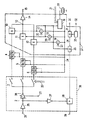
図1は同調器 101、変調器 102、及び分波器 103の組合せを示しており、その中で変調器 102と分波器 103とが分波器‐変調器を形成するために組み合わされている。無線周波数入力信号、例えばテレビジョン信号が、無線周波数信号入力端子 104を介して、アンテナから分波器 103へ印加され得る。この信号が第1前置増幅器 105を介して第1信号分波器 106へ印加され、且つこの分波器から第1ライン 107へ、及び第2前置増幅器 108を介して第2信号分波器 109へ印加される。この信号は無線周波数出力端子 110を介して分波器から供給され得る。
【0009】
無線周波数入力信号は、第1ライン 107を通って同調器 101へ印加され、同調器内では周波数選択 111、振幅制御 112、及びダウン変換 113がこの目的のために慣習的に用いられる段により、慣習的に実行される。中間周波数信号が出力増幅器14を介して供給される。同調器 101と関係し、且つ位相ロックループ 115と発振器段 116とを具えている振動発生器からの基準振動が、周波数選択段 111とダウン変換段 113へ慣習的な方法で印加される。位相ロックループ 115が同調器 101を同調する目的にために、制御ライン 117、好適には I2Cバスを介して制御できる。
【0010】
変調器 102は既知のオーディオ信号変調器33を具えており、それのオーディオ信号入力端子32が、音声搬送波振動上で変調されたオーディオベースバンド信号を受信できる。変調されたオーディオ信号が、入力端子30を介して供給されたベースバンドビデオ信号上に、低周波数信号重畳段31において重畳される。かくして得られたFBAS信号が変調器段35において無線周波数搬送波振動上で変調され、その振動は変調器 102の振動発生器において発生され、その振動発生器は第2位相ロックループ 123と第2発振器段 124とを具えている。原理的には変調器 102の振動発生器123, 124は、同調器 101に対する構造と同じ構造を有している。特に、双方の振動発生器115, 116及び123, 124は、単一水晶発振器により制御されるが、一方振動と低オーミック結合とを増幅するためのトランジスタ結合段 126が、水晶発振器22と第2位相ロックループ 123との間に配設されてもよい。
【0011】
第2ライン 127が、変調器 102の無線周波数出力信号を変調器段35から分波器 103の第2信号分波器 109へ供給し、その分波器を介して無線周波数出力信号が無線周波数信号出力端子 110へ到達する。
【0012】
図2に示された実施例は、無線周波数信号用の入力端子2へ入力端子においてと切換段3へ出力端子において接続された広帯域幅入力増幅器1と、前記切換段3へ接続され且つ信号接合点により終わらされる、3個の信号処理分枝とを具えている。図2における各信号処理分枝は、切換段3へ接続されたフィルタ段4,5及び6と、それらのフィルタ段4,5及び6へ接続された可制御増幅器段7,8及び9、及び関連する可制御増幅器段7,8及び9へ接続されたミクサ段10, 11及び12をそれぞれ具えている。無線周波数信号は、信号処理分枝のうちの一つへ任意に、広帯域幅入力増幅器と切換段3とを介して、入力端子2から印加される。その信号処理分枝において、その信号処理分枝において、信号処理分枝と関連する所望の周波数帶域がフィルタ段4,5又は6において選択される。可制御増幅器段7,8,9を介して、濾波された周波数帶域のみの無線周波数信号がミクサ段10, 11及び12へ印加され、且つミクサ段10, 11及び12において周波数がダウン変換される。結合点13と出力増幅器14とにより図2の装置で形成された信号接合点が、ダウン変換された無線周波数信号が共通出力端子15へ供給されることを可能にする。この信号接合点は代わりに結合点のみを具えてもよく、出力端子15と一緒に、その時出力増幅器14が全部の信号処理分枝に対して共通である出力分枝と関連する。
【0013】
無線周波数をダウン変換するために必要な振動を発生するために、共通振動発生器が図2の装置においては用いられて、その振動発生器は、全部の信号処理分枝に対して共通である位相ロックループ16と、各信号処理分枝に対して別々の発振器段17, 18, 19とを具えている。位相ロックループ16と発振器段17, 18, 19とは既知の方法で相互接続されている。信号処理分枝間の混信を除外するために、発振器段17, 18, 19がデータライン20を介して任意にスイッチオン又はオフさてもよいので、一つの振動のみが(入力増幅器1を介して)入力端子2へ切換段3を介して信号処理分枝が接続さている発振器段17, 18, 19により供給される。その時データライン20も同じ方法で切換段3へ接続され得る。更に、振動発生器17〜19により供給される振動の周波数は、位相ロックループ16のデータ入力端子21を介して調節できる。振動発生器17〜19は更に周波数基準としての水晶発振器22へも接続さている。
【0014】
可制御増幅器段7,8,9はその増幅器段7,8,9の利得率がそれを介して調節できる制御入力端子23を有している。その時可制御増幅器段7,8,9は無線周波数信号の振幅又は出力制御のために制御ループないに挿入されてもよい。
【0015】
位相ロックループ16のデータ入力端子21と同時にデータライン20が同調器の受信機動作のための制御器(図示せず)へ接続されてもよい。
【0016】
フィルタ段4,5,6は位相ロックループ16のライン24を介して接続されている。このライン24を介して、振動発生器17〜19による周波数選択のための信号は慣習的な方法で供給され得る。特に、フィルタ段4,5,6内の同調ダイオードは発振器段17, 18, 19と同じ方法で同調される。
【0017】
図2は更にビデオレコーダの無線信号処理ユニットにおける先の実施例に記載された同調器の挿入を示している。この目的のために、図2はビデオレコーダのアンテナ入力端子26への入力端子と無線周波数信号用の同調器の入力端子2への出力端子とで接続されている別の入力増幅器段25を示している。入力端子2は更に無線周波数信号重畳段28の入力端子へ橋絡増幅器27を介して接続されている。無線周波数信号重畳段の出力端子がビデオレコーダのアンテナ出力端子29を構成している。
【0018】
ベースバンドビデオ信号用の入力端子30が低周波数信号重畳段31の第1入力端子を構成している。オーディオ信号用の入力端子32がオーディオ信号変調器段33へ接続されている。この段は低周波数信号重畳段31の第2入力端子へ接続さている。オーディオ信号変調器段33において、入力端子32から供給されたオーディオ信号が副搬送波振動上で変調され且つ次に付加的に低周波数信号重畳段31においてベースバンドビデオ信号上に重畳される。この方法で、FBAS信号が発生され且つ低周波数信号重畳段31の出力端子34を介して供給される。この出力端子34が変調器段35へ接続されて、その段においてFBAS信号が発振器段のうちの一つ、ここでは第3信号処理分枝用の発振器段19からの振動によりアップ変換される。ビデオレコーダのアンテナ出力端子29へ更に供給するために無線周波数信号重畳段28へ印加される無線周波数信号がそれで産出される。
【0019】
図2において、破線36内の要素は構成要素の統合された群へ好都合に組み合わされる。対応する方法で、鎖線37内の要素は構成要素の別の統合された群へ組み合わされてもよい。これらの統合された群は半導体本体上に個々に統合されてもよい。
【0020】
図3は本発明による同調器の第2実施例を示している。図2に示された実施例と比較すると、広帯域幅入力増幅器1が広帯域幅可制御入力増幅器38より置き換えられ、その増幅器は無線周波数信号の振幅及び出力制御の目的のために制御入力端子23へ接続されているだけである。これに反して、信号処理分枝内の可制御増幅器段7,8,9は廃止され、図3の修正においては、それらは別の信号増幅又は反射減衰量減衰がそれらの位置で望まれるかぎり、一定利得率を有する増幅器段によりそれらが置き換えられてもよい。
【0021】
その他の点では、図2及び3に示された実施例は同じである。
【0022】
今までに説明された図においては、同調器 101が図2及び3において参照符号3〜13により表された要素を具え、変調器 102が要素30〜35を具え、且つ分波器 103が図2及び3に示された実施例においては要素1,2,25, 27及び28を好適に具えている。図1に示された分波器は信号を分割するのみならず、機能が図2及び3における無線周波数信号重畳段28に対応する第2信号分波器 109によって信号を組み合わせるので、それは分波器‐コンバイナーと呼ばれてもよい。その時第1信号分波器 106が無線周波数信号用の入力端子2の機能を引き継ぐ。更に無線周波数信号入力端子 104がビデオレコーダのアンテナ入力端子26と対応し、第1増幅器 105が別の入力増幅器段25に対応し、第2前置増幅器 108が橋絡増幅器27に対応し、且つ無線周波数信号出力端子 110がビデオレコーダのアンテナ出力端子29に対応する。図1における周波数選択 111は図2及び3におけるフィルタ段4〜6により実行され、且つ振幅制御 112は可制御増幅器段7〜9により実行され、一方ダウン変換 113はミクサ段10〜12において実行される。図2及び3において、データ入力端子21が図1の制御ライン 117の機能を満たす。
【0023】
本発明は衛星受信機及びビデオレコーダの無線周波数処理段内に好適に用いられる。
【図面の簡単な説明】
【図1】種々の用語を説明するために、欧州特許出願第95 200 961.1に記載されたような回路装置を示している。
【図2】本発明による第1実施例を示している。
【図3】本発明による第2実施例を示している。
【符号の説明】
1 広帯域幅入力増幅器
2 無線周波数信号用の入力端子
3 切換段
4,5,6 フィルタ段
7,8,9 可制御増幅器段
10, 11,12 ミクサ段
13 結合点
14 出力増幅器
15 共通出力端子
16 位相ロックループ
17, 18, 19 発振器段
20 データライン
21 位相ロックループのデータ入力端子
22 水晶発振器
23 制御入力端子
24 位相ロックループのライン
25 入力増幅器段
26 ビデオレコーダのアンテナ入力端子
27 橋絡増幅器
28 無線周波数信号重畳段
29 ビデオレコーダのアンテナ出力端子
30 ベースバンドビデオ信号用の入力端子
31 低周波数信号重畳段
32 オーディオ信号用の入力端子
33 オーディオ信号変調器段
34 低周波数信号重畳段の出力端子
35 変調器段
36 破線
37 鎖線
38 広帯域幅可制御入力増幅器
101 同調器
102 変調器
103 分波器
104 無線周波数信号入力端子
105 第1前置増幅器
106 第1信号分波器
107 第1ライン
108 第2前置増幅器
109 第2信号分波器
110 無線周波数出力端子
111 周波数選択段
112 振幅制御段
113 ダウン変換段
115 位相ロックループ
116 発振器段
117 制御ライン
123 第2位相ロックループ
124 第2発振器段
126 トランジスタ結合段
127 第2ライン[0001]
BACKGROUND OF THE INVENTION
The present invention relates to a circuit arrangement comprising a demultiplexer-modulator comprising a tuner and a demultiplexer and a modulator, in which the demultiplexer applies a radio frequency input signal. A radio frequency input terminal, a radio frequency signal output terminal for supplying a radio frequency output signal, a first line for applying the radio frequency input signal to the tuner, and a radio frequency output signal from the modulator The tuner is adapted to demodulate the radio frequency input signal and the modulator converts the baseband signal into a radio frequency output signal to be supplied by the modulator. And the circuit arrangement comprises a device for generating a reference vibration for the tuner and duplexer-modulator, said device comprising a tuner and a duplexer-modulator Common to There are at least one of the quartz crystal, and tuner and demultiplexer - have a phase-locked loop is common to the modulator.
[0002]
[Prior art]
Such a circuit arrangement is described in European Patent Application No. 95 200 961.1. The purpose of this circuit arrangement described in said application is the use of a small number of components for a circuit arrangement comprising both a tuner and a duplexer-modulator. In particular, devices with a small number of components use only one vibration generator with a single oscillator stage for both the modulator and tuner in the duplexer.
[0003]
In order to tune a tuner for different transmitters, it is necessary to synchronize the adjustment of the filter stage and the adjustment of the oscillator stage in the tuner, which places strict requirements on the quality of the signal processing. In some cases, the use of multiple components is required in dimensioning the tuning elements of the filter stage and the oscillator stage.
[0004]
[Problems to be solved by the invention]
It is an object of the present invention to achieve a structure that is as compact as possible by using a minimal number of components at low manufacturing costs in circuit devices of the type described so far.
[0005]
[Means for Solving the Problems]
In the circuit arrangement according to the invention, the tuner comprises at least one signal processing branch for frequency selective reception and / or amplification and / or frequency conversion of radio frequency signals in each frequency range, And a device for generating a reference vibration (vibration generator) comprises a separate oscillator stage for each signal processing branch, one of these oscillator stages being the reference for the duplexer-modulator This purpose is achieved by being also used to generate vibrations.
[0006]
In the circuit arrangement according to the invention, a separate oscillator stage is thus used for each frequency band in each associated signal processing branch. This stage can be best adapted to the filter stage of this signal processing branch. This avoids a very precise adaptation of a single oscillator stage to filter stages of different signal processing branches for different frequency bands. On the other hand, one of the oscillator stages is also used for a modulator for supplying the necessary carrier oscillation. If there are multiple signal processing branches and multiple frequency bands in the tuner, depending on the frequency range in which the modulator must supply the radio frequency output signal, the modulator is an appropriate oscillator. Can be connected to a stage. The operation of this circuit arrangement is particularly simplified by operating only either the tuner or the modulator. However, the present invention offers the possibility of simultaneous operation.
[0007]
DETAILED DESCRIPTION OF THE INVENTION
These aspects will become apparent from the examples described below, and other aspects will be described with reference to the examples described below.
[0008]
FIG. 1 shows a combination of a
[0009]
The radio frequency input signal is applied to
[0010]
The
[0011]
The
[0012]
The embodiment shown in FIG. 2 comprises a wide bandwidth input amplifier 1 connected at the input terminal to the input terminal 2 for radio frequency signals and at the output terminal to the
[0013]
In order to generate the vibrations necessary to downconvert the radio frequency, a common vibration generator is used in the apparatus of FIG. 2, which is common to all signal processing branches. A
[0014]
The
[0015]
Simultaneously with the
[0016]
Filter stages 4, 5, 6 are connected via
[0017]
FIG. 2 further shows the insertion of the tuner described in the previous embodiment in the radio signal processing unit of the video recorder. For this purpose, FIG. 2 shows another
[0018]
The baseband video
[0019]
In FIG. 2, the elements within dashed
[0020]
FIG. 3 shows a second embodiment of a tuner according to the invention. Compared to the embodiment shown in FIG. 2, the wide bandwidth input amplifier 1 is replaced by a wide bandwidth controllable input amplifier 38, which is connected to the
[0021]
In other respects, the embodiments shown in FIGS. 2 and 3 are the same.
[0022]
In the figures described so far,
[0023]
The present invention is preferably used in the radio frequency processing stage of satellite receivers and video recorders.
[Brief description of the drawings]
FIG. 1 shows a circuit arrangement as described in European Patent Application No. 95 200 961.1 to illustrate various terms.
FIG. 2 shows a first embodiment according to the present invention.
FIG. 3 shows a second embodiment according to the present invention.
[Explanation of symbols]
DESCRIPTION OF SYMBOLS 1 Wide bandwidth input amplifier 2
10, 11, 12 Mixer stage
13 attachment points
14 Output amplifier
15 Common output terminal
16 Phase lock loop
17, 18, 19 Oscillator stage
20 data lines
21 Phase lock loop data input pin
22 Crystal oscillator
23 Control input terminal
24 Phase Lock Loop Line
25 Input amplifier stage
26 Video recorder antenna input terminal
27 Bridge amplifier
28 Radio frequency signal superposition stage
29 Video recorder antenna output terminal
30 Input terminal for baseband video signal
31 Low frequency signal superposition stage
32 Audio signal input terminals
33 Audio signal modulator stage
34 Output terminal of low frequency signal superimposing stage
35 Modulator stage
36 Dashed line
37 Chain line
38 Wide bandwidth controllable input amplifier
101 Tuner
102 modulator
103 duplexer
104 Radio frequency signal input terminal
105 First preamplifier
106 First signal duplexer
107 First line
108 Second preamplifier
109 Second signal duplexer
110 Radio frequency output terminal
111 Frequency selection stage
112 Amplitude control stage
113 Down conversion stage
115 phase-locked loop
116 Oscillator stage
117 Control line
123 Second phase lock loop
124 Second oscillator stage
126 Transistor coupling stage
127 2nd line
Claims (1)
前記同調器が、各々の周波数帯の前記無線周波数信号の周波数選択受信、増幅及び/又は周波数変換に関する少なくとも1つの信号処理分枝を具え、前記基準振動を発生する装置(振動発生器)が、各々の信号処理分枝ごとに別個の発振器段を具え、これらの発振器段のうち1つを、前記分波器−変調器に関する基準振動の発生にも使用することを特徴とする回路装置。A circuit device comprising a tuner and a duplexer-modulator comprising a duplexer and a modulator, wherein the duplexer applies a radio frequency input signal, a radio frequency signal input unit, and a radio A radio frequency signal output unit for supplying a frequency output signal; a first line for applying the radio frequency input signal to the tuner; and a second line for supplying a radio frequency output signal from the modulator; A tuner is adapted to demodulate the radio frequency input signal, and the modulator is adapted to convert a baseband signal to the radio frequency output signal to be provided by the modulator, the circuit arrangement comprising: A device for generating a reference oscillation for said tuner and duplexer-modulator, said device comprising at least one crystal common to said tuner and duplexer-modulator, said tuner and splitter Waver-weird And a common phase-locked loop with respect to the vessel, in the circuit device,
An apparatus (vibration generator) for generating the reference vibration, wherein the tuner comprises at least one signal processing branch for frequency selective reception, amplification and / or frequency conversion of the radio frequency signal in each frequency band; A circuit arrangement comprising a separate oscillator stage for each signal processing branch, wherein one of these oscillator stages is also used for generating a reference oscillation for said duplexer-modulator.
Applications Claiming Priority (2)
| Application Number | Priority Date | Filing Date | Title |
|---|---|---|---|
| DE19538544A DE19538544A1 (en) | 1995-10-17 | 1995-10-17 | Circuit arrangement with a high-frequency reception stage and a transmission stage |
| DE19538544:6 | 1995-10-17 |
Publications (2)
| Publication Number | Publication Date |
|---|---|
| JPH09135152A JPH09135152A (en) | 1997-05-20 |
| JP3816995B2 true JP3816995B2 (en) | 2006-08-30 |
Family
ID=7775015
Family Applications (1)
| Application Number | Title | Priority Date | Filing Date |
|---|---|---|---|
| JP27338696A Expired - Fee Related JP3816995B2 (en) | 1995-10-17 | 1996-10-16 | Circuit device with tuner and duplexer-modulator. |
Country Status (6)
| Country | Link |
|---|---|
| US (1) | US5867771A (en) |
| EP (1) | EP0769872B1 (en) |
| JP (1) | JP3816995B2 (en) |
| KR (1) | KR100441183B1 (en) |
| DE (2) | DE19538544A1 (en) |
| SG (1) | SG55235A1 (en) |
Families Citing this family (9)
| Publication number | Priority date | Publication date | Assignee | Title |
|---|---|---|---|---|
| US6442382B1 (en) * | 1997-06-27 | 2002-08-27 | Agere Systems Guardian Corp. | Filter switching system and method |
| DE19728315A1 (en) * | 1997-07-03 | 1999-01-07 | Philips Patentverwaltung | TV signal receiver |
| US6405025B1 (en) * | 1997-12-09 | 2002-06-11 | Nokia Mobile Phones Limited | Method for selecting the frequency range in radio communication devices operating in several frequency ranges and a radio communication device |
| JP2002118795A (en) * | 2000-10-05 | 2002-04-19 | Alps Electric Co Ltd | Television signal reception tuner |
| JP3719926B2 (en) * | 2000-11-14 | 2005-11-24 | シャープ株式会社 | Digital signal receiving tuner |
| GB0122983D0 (en) * | 2001-09-25 | 2001-11-14 | Zarlink Semiconductor Ltd | Rdio fequency tuner front end and tuner |
| US7024220B2 (en) * | 2001-10-09 | 2006-04-04 | Kyocera Wireless Corp. | GPS receiver system and method |
| DE10163798A1 (en) * | 2001-12-22 | 2003-07-03 | Philips Intellectual Property | TV signal receiver with universal output for various surface wave filters |
| US8750441B2 (en) * | 2010-12-20 | 2014-06-10 | Texas Instruments Incorporated | Signal cancellation to reduce phase noise, period jitter, and other contamination in local oscillator, frequency timing, or other timing generators or signal sources |
Family Cites Families (10)
| Publication number | Priority date | Publication date | Assignee | Title |
|---|---|---|---|---|
| US4157505A (en) * | 1977-06-13 | 1979-06-05 | Regency Electronics | Plural band scanning radio with direct switch of RF amplifying transistors |
| US4379271A (en) * | 1980-08-25 | 1983-04-05 | Rca Corporation | Input selection arrangement for applying different local oscillator signals to a prescaler of a phase-lock loop tuning system |
| US4667243A (en) * | 1985-10-31 | 1987-05-19 | Rca Corporation | Television receiver for direct broadcast satellite signals |
| US4894720A (en) * | 1987-07-31 | 1990-01-16 | Sanyo Electric Co., Ltd. | Circuit for selectively outputting high frequency signals |
| DE3728381A1 (en) * | 1987-08-26 | 1989-03-09 | Thomson Brandt Gmbh | CIRCUIT ARRANGEMENT FOR DISTRIBUTING AN ANTENNA SIGNAL |
| DE3821714A1 (en) * | 1988-06-28 | 1990-01-04 | Telefunken Electronic Gmbh | TELEVISION TUNER |
| US5420646A (en) * | 1991-12-30 | 1995-05-30 | Zenith Electronics Corp. | Bandswitched tuning system having a plurality of local oscillators for a digital television receiver |
| DE19509567A1 (en) * | 1994-04-21 | 1995-10-26 | Philips Patentverwaltung | Radio frequency reception stage |
| EP0678981A3 (en) * | 1994-04-21 | 1996-05-15 | Philips Patentverwaltung | High-frequency receiving stage. |
| US5758266A (en) * | 1994-09-30 | 1998-05-26 | Qualcomm Incorporated | Multiple frequency communication device |
-
1995
- 1995-10-17 DE DE19538544A patent/DE19538544A1/en not_active Withdrawn
-
1996
- 1996-10-11 DE DE59608783T patent/DE59608783D1/en not_active Expired - Lifetime
- 1996-10-11 EP EP96202842A patent/EP0769872B1/en not_active Expired - Lifetime
- 1996-10-16 JP JP27338696A patent/JP3816995B2/en not_active Expired - Fee Related
- 1996-10-16 SG SG1996010870A patent/SG55235A1/en unknown
- 1996-10-17 US US08/733,307 patent/US5867771A/en not_active Expired - Lifetime
- 1996-10-17 KR KR1019960046394A patent/KR100441183B1/en not_active IP Right Cessation
Also Published As
| Publication number | Publication date |
|---|---|
| DE19538544A1 (en) | 1997-04-24 |
| DE59608783D1 (en) | 2002-04-04 |
| US5867771A (en) | 1999-02-02 |
| JPH09135152A (en) | 1997-05-20 |
| KR970024552A (en) | 1997-05-30 |
| EP0769872B1 (en) | 2002-02-27 |
| EP0769872A2 (en) | 1997-04-23 |
| EP0769872A3 (en) | 1997-05-02 |
| SG55235A1 (en) | 1999-07-20 |
| KR100441183B1 (en) | 2004-10-08 |
Similar Documents
| Publication | Publication Date | Title |
|---|---|---|
| EP0911962A1 (en) | Cable modem tuner | |
| JP2002026758A (en) | Receiver system and its method using analog/digital conversion for radio frequency | |
| JP3816995B2 (en) | Circuit device with tuner and duplexer-modulator. | |
| CN105027452B (en) | Reception device and electronic equipment | |
| JP4699336B2 (en) | Wireless receiver and electronic device | |
| US5640688A (en) | Tuner and splitter-modulator circuit having a common quartz crystal | |
| JPH01243614A (en) | Distribution circuit device of antenna signal | |
| US7343015B2 (en) | Method and apparatus for high fidelity wireless stereophonic transmission utilizing dual frequency carriers | |
| JPS5997233A (en) | Direct mixing synchronous receiver | |
| US4633513A (en) | Method and apparatus for converting television signals | |
| US4647875A (en) | Ultrahigh frequency active filter | |
| JPS63152231A (en) | Rf converter circuit | |
| JP3502263B2 (en) | Tuner for digital broadcasting reception | |
| JPH07321603A (en) | Tuner | |
| JP4138639B2 (en) | Microwave wireless communication system and electronic device | |
| JPH09135187A (en) | Tuner | |
| KR100506733B1 (en) | Analog/digital television tuner | |
| JP3495661B2 (en) | Receiver | |
| JP3091206B2 (en) | Space diversity receiving system | |
| JP2004533782A (en) | Device for down-converting signal frequency | |
| KR950014650B1 (en) | Distribution system of u.h.f. signal | |
| JP3188398B2 (en) | Antenna with phase synthesizer | |
| JP3495656B2 (en) | Receiver | |
| JPH1070439A (en) | Receiver | |
| JP3134801B2 (en) | Shared receiver |
Legal Events
| Date | Code | Title | Description |
|---|---|---|---|
| A977 | Report on retrieval |
Free format text: JAPANESE INTERMEDIATE CODE: A971007 Effective date: 20060421 |
|
| TRDD | Decision of grant or rejection written | ||
| A01 | Written decision to grant a patent or to grant a registration (utility model) |
Free format text: JAPANESE INTERMEDIATE CODE: A01 Effective date: 20060509 |
|
| A61 | First payment of annual fees (during grant procedure) |
Free format text: JAPANESE INTERMEDIATE CODE: A61 Effective date: 20060609 |
|
| R150 | Certificate of patent or registration of utility model |
Free format text: JAPANESE INTERMEDIATE CODE: R150 |
|
| S111 | Request for change of ownership or part of ownership |
Free format text: JAPANESE INTERMEDIATE CODE: R313113 |
|
| R371 | Transfer withdrawn |
Free format text: JAPANESE INTERMEDIATE CODE: R371 |
|
| S111 | Request for change of ownership or part of ownership |
Free format text: JAPANESE INTERMEDIATE CODE: R313113 |
|
| R350 | Written notification of registration of transfer |
Free format text: JAPANESE INTERMEDIATE CODE: R350 |
|
| FPAY | Renewal fee payment (event date is renewal date of database) |
Free format text: PAYMENT UNTIL: 20100616 Year of fee payment: 4 |
|
| FPAY | Renewal fee payment (event date is renewal date of database) |
Free format text: PAYMENT UNTIL: 20110616 Year of fee payment: 5 |
|
| FPAY | Renewal fee payment (event date is renewal date of database) |
Free format text: PAYMENT UNTIL: 20120616 Year of fee payment: 6 |
|
| S111 | Request for change of ownership or part of ownership |
Free format text: JAPANESE INTERMEDIATE CODE: R313113 |
|
| R371 | Transfer withdrawn |
Free format text: JAPANESE INTERMEDIATE CODE: R371 |
|
| FPAY | Renewal fee payment (event date is renewal date of database) |
Free format text: PAYMENT UNTIL: 20120616 Year of fee payment: 6 |
|
| S111 | Request for change of ownership or part of ownership |
Free format text: JAPANESE INTERMEDIATE CODE: R313113 |
|
| FPAY | Renewal fee payment (event date is renewal date of database) |
Free format text: PAYMENT UNTIL: 20120616 Year of fee payment: 6 |
|
| R350 | Written notification of registration of transfer |
Free format text: JAPANESE INTERMEDIATE CODE: R350 |
|
| FPAY | Renewal fee payment (event date is renewal date of database) |
Free format text: PAYMENT UNTIL: 20130616 Year of fee payment: 7 |
|
| LAPS | Cancellation because of no payment of annual fees |