JP3816396B2 - Switching power supply - Google Patents
Switching power supply Download PDFInfo
- Publication number
- JP3816396B2 JP3816396B2 JP2002006995A JP2002006995A JP3816396B2 JP 3816396 B2 JP3816396 B2 JP 3816396B2 JP 2002006995 A JP2002006995 A JP 2002006995A JP 2002006995 A JP2002006995 A JP 2002006995A JP 3816396 B2 JP3816396 B2 JP 3816396B2
- Authority
- JP
- Japan
- Prior art keywords
- circuit
- power supply
- voltage
- operating voltage
- control circuit
- Prior art date
- Legal status (The legal status is an assumption and is not a legal conclusion. Google has not performed a legal analysis and makes no representation as to the accuracy of the status listed.)
- Expired - Fee Related
Links
Images


Classifications
-
- H—ELECTRICITY
- H02—GENERATION; CONVERSION OR DISTRIBUTION OF ELECTRIC POWER
- H02M—APPARATUS FOR CONVERSION BETWEEN AC AND AC, BETWEEN AC AND DC, OR BETWEEN DC AND DC, AND FOR USE WITH MAINS OR SIMILAR POWER SUPPLY SYSTEMS; CONVERSION OF DC OR AC INPUT POWER INTO SURGE OUTPUT POWER; CONTROL OR REGULATION THEREOF
- H02M3/00—Conversion of DC power input into DC power output
- H02M3/22—Conversion of DC power input into DC power output with intermediate conversion into AC
- H02M3/24—Conversion of DC power input into DC power output with intermediate conversion into AC by static converters
- H02M3/28—Conversion of DC power input into DC power output with intermediate conversion into AC by static converters using discharge tubes with control electrode or semiconductor devices with control electrode to produce the intermediate AC
-
- H—ELECTRICITY
- H02—GENERATION; CONVERSION OR DISTRIBUTION OF ELECTRIC POWER
- H02M—APPARATUS FOR CONVERSION BETWEEN AC AND AC, BETWEEN AC AND DC, OR BETWEEN DC AND DC, AND FOR USE WITH MAINS OR SIMILAR POWER SUPPLY SYSTEMS; CONVERSION OF DC OR AC INPUT POWER INTO SURGE OUTPUT POWER; CONTROL OR REGULATION THEREOF
- H02M1/00—Details of apparatus for conversion
- H02M1/0003—Details of control, feedback or regulation circuits
- H02M1/0006—Arrangements for supplying an adequate voltage to the control circuit of converters
-
- H—ELECTRICITY
- H02—GENERATION; CONVERSION OR DISTRIBUTION OF ELECTRIC POWER
- H02M—APPARATUS FOR CONVERSION BETWEEN AC AND AC, BETWEEN AC AND DC, OR BETWEEN DC AND DC, AND FOR USE WITH MAINS OR SIMILAR POWER SUPPLY SYSTEMS; CONVERSION OF DC OR AC INPUT POWER INTO SURGE OUTPUT POWER; CONTROL OR REGULATION THEREOF
- H02M1/00—Details of apparatus for conversion
- H02M1/0067—Converter structures employing plural converter units, other than for parallel operation of the units on a single load
- H02M1/007—Plural converter units in cascade
-
- H—ELECTRICITY
- H02—GENERATION; CONVERSION OR DISTRIBUTION OF ELECTRIC POWER
- H02M—APPARATUS FOR CONVERSION BETWEEN AC AND AC, BETWEEN AC AND DC, OR BETWEEN DC AND DC, AND FOR USE WITH MAINS OR SIMILAR POWER SUPPLY SYSTEMS; CONVERSION OF DC OR AC INPUT POWER INTO SURGE OUTPUT POWER; CONTROL OR REGULATION THEREOF
- H02M1/00—Details of apparatus for conversion
- H02M1/36—Means for starting or stopping converters
-
- H—ELECTRICITY
- H02—GENERATION; CONVERSION OR DISTRIBUTION OF ELECTRIC POWER
- H02M—APPARATUS FOR CONVERSION BETWEEN AC AND AC, BETWEEN AC AND DC, OR BETWEEN DC AND DC, AND FOR USE WITH MAINS OR SIMILAR POWER SUPPLY SYSTEMS; CONVERSION OF DC OR AC INPUT POWER INTO SURGE OUTPUT POWER; CONTROL OR REGULATION THEREOF
- H02M3/00—Conversion of DC power input into DC power output
- H02M3/22—Conversion of DC power input into DC power output with intermediate conversion into AC
- H02M3/24—Conversion of DC power input into DC power output with intermediate conversion into AC by static converters
- H02M3/28—Conversion of DC power input into DC power output with intermediate conversion into AC by static converters using discharge tubes with control electrode or semiconductor devices with control electrode to produce the intermediate AC
- H02M3/325—Conversion of DC power input into DC power output with intermediate conversion into AC by static converters using discharge tubes with control electrode or semiconductor devices with control electrode to produce the intermediate AC using devices of a triode or a transistor type requiring continuous application of a control signal
- H02M3/335—Conversion of DC power input into DC power output with intermediate conversion into AC by static converters using discharge tubes with control electrode or semiconductor devices with control electrode to produce the intermediate AC using devices of a triode or a transistor type requiring continuous application of a control signal using semiconductor devices only
- H02M3/33569—Conversion of DC power input into DC power output with intermediate conversion into AC by static converters using discharge tubes with control electrode or semiconductor devices with control electrode to produce the intermediate AC using devices of a triode or a transistor type requiring continuous application of a control signal using semiconductor devices only having several active switching elements
- H02M3/33576—Conversion of DC power input into DC power output with intermediate conversion into AC by static converters using discharge tubes with control electrode or semiconductor devices with control electrode to produce the intermediate AC using devices of a triode or a transistor type requiring continuous application of a control signal using semiconductor devices only having several active switching elements having at least one active switching element at the secondary side of an isolation transformer
- H02M3/33592—Conversion of DC power input into DC power output with intermediate conversion into AC by static converters using discharge tubes with control electrode or semiconductor devices with control electrode to produce the intermediate AC using devices of a triode or a transistor type requiring continuous application of a control signal using semiconductor devices only having several active switching elements having at least one active switching element at the secondary side of an isolation transformer having a synchronous rectifier circuit or a synchronous freewheeling circuit at the secondary side of an isolation transformer
-
- H—ELECTRICITY
- H02—GENERATION; CONVERSION OR DISTRIBUTION OF ELECTRIC POWER
- H02M—APPARATUS FOR CONVERSION BETWEEN AC AND AC, BETWEEN AC AND DC, OR BETWEEN DC AND DC, AND FOR USE WITH MAINS OR SIMILAR POWER SUPPLY SYSTEMS; CONVERSION OF DC OR AC INPUT POWER INTO SURGE OUTPUT POWER; CONTROL OR REGULATION THEREOF
- H02M3/00—Conversion of DC power input into DC power output
- H02M3/22—Conversion of DC power input into DC power output with intermediate conversion into AC
- H02M3/24—Conversion of DC power input into DC power output with intermediate conversion into AC by static converters
- H02M3/28—Conversion of DC power input into DC power output with intermediate conversion into AC by static converters using discharge tubes with control electrode or semiconductor devices with control electrode to produce the intermediate AC
- H02M3/325—Conversion of DC power input into DC power output with intermediate conversion into AC by static converters using discharge tubes with control electrode or semiconductor devices with control electrode to produce the intermediate AC using devices of a triode or a transistor type requiring continuous application of a control signal
- H02M3/335—Conversion of DC power input into DC power output with intermediate conversion into AC by static converters using discharge tubes with control electrode or semiconductor devices with control electrode to produce the intermediate AC using devices of a triode or a transistor type requiring continuous application of a control signal using semiconductor devices only
- H02M3/337—Conversion of DC power input into DC power output with intermediate conversion into AC by static converters using discharge tubes with control electrode or semiconductor devices with control electrode to produce the intermediate AC using devices of a triode or a transistor type requiring continuous application of a control signal using semiconductor devices only in push-pull configuration
- H02M3/3376—Conversion of DC power input into DC power output with intermediate conversion into AC by static converters using discharge tubes with control electrode or semiconductor devices with control electrode to produce the intermediate AC using devices of a triode or a transistor type requiring continuous application of a control signal using semiconductor devices only in push-pull configuration with automatic control of output voltage or current
-
- Y—GENERAL TAGGING OF NEW TECHNOLOGICAL DEVELOPMENTS; GENERAL TAGGING OF CROSS-SECTIONAL TECHNOLOGIES SPANNING OVER SEVERAL SECTIONS OF THE IPC; TECHNICAL SUBJECTS COVERED BY FORMER USPC CROSS-REFERENCE ART COLLECTIONS [XRACs] AND DIGESTS
- Y02—TECHNOLOGIES OR APPLICATIONS FOR MITIGATION OR ADAPTATION AGAINST CLIMATE CHANGE
- Y02B—CLIMATE CHANGE MITIGATION TECHNOLOGIES RELATED TO BUILDINGS, e.g. HOUSING, HOUSE APPLIANCES OR RELATED END-USER APPLICATIONS
- Y02B70/00—Technologies for an efficient end-user side electric power management and consumption
- Y02B70/10—Technologies improving the efficiency by using switched-mode power supplies [SMPS], i.e. efficient power electronics conversion e.g. power factor correction or reduction of losses in power supplies or efficient standby modes
Landscapes
- Engineering & Computer Science (AREA)
- Power Engineering (AREA)
- Dc-Dc Converters (AREA)
Description
【0001】
【発明の属する技術分野】
本発明は、スイッチング電源装置に関し、さらに詳細には、動作停止時における出力電圧Voutのアンダーシュートや振動が防止されたスイッチング電源装置に関する。
【0002】
【従来の技術】
従来より、コンピュータに代表される電子機器・電気機器の電源装置としてスイッチング電源装置が広く用いられている。
【0003】
図7は、従来のスイッチング電源装置の回路である。
【0004】
図7に示すように、従来のスイッチング電源装置は、トランスT1と、トランスT1の1次側に設けられたハーフブリッジ型のスイッチング回路と、トランスT1の2次側に設けられた自己ドライブ型の整流回路及び平滑回路とを備え、1次側のスイッチング回路に供給される直流入力電圧Vinを降圧して直流出力電圧Voutを生成し、これを負荷に供給する装置である。負荷は、図7に示すように、抵抗成分RLoadと容量成分CLoadとリアクトル成分LLoadによって表される。
【0005】
1次側のスイッチング回路を構成するメインスイッチQ1、Q2の動作は、出力電圧Voutに基づいて制御回路10により制御される。より具体的には、制御回路10は、出力電圧Voutが目標電圧と比べて高くなるほどメインスイッチQ1、Q2のデューティを低下させることによって負荷に供給される電力を減らし、逆に、出力電圧Voutが目標電圧と比べて低くなるほどメインスイッチQ1、Q2のデューティを上昇させることによって負荷に供給される電力を増やす。このようにして、負荷に与えられる出力電圧Voutの値が常に上記目標電圧となるように制御される。尚、制御回路10は1次側回路に属するため、出力電圧Voutを直接受けることはできず、図7に示すように、絶縁回路20を介して出力電圧Voutに連動する電圧Vout’が制御回路10に与えられる。
【0006】
制御回路10の動作電圧Vccは、トランジスタTr1、抵抗R1及びツェナーダイオードZ1からなる動作電圧生成回路によって生成される。制御回路10の電源端子間に接続されているコンデンサC3は、動作電圧Vccの安定化を目的とした平滑コンデンサである。かかる動作電圧生成回路は、動作スイッチS1がオンであると活性状態となり、動作スイッチS1がオフであると非活性状態となる。動作スイッチS1のオン/オフは、外部から任意に切り替えることができ、図7に示すスイッチング電源装置を動作させたい場合には、外部から動作スイッチS1をオンさせ、スイッチング電源装置の動作を停止させたい場合には、外部から動作スイッチS1をオフさせればよい。
【0007】
一方、2次側の整流回路を構成する整流スイッチQ3、Q4は、トランスT1の2次側電圧によって自己ドライブされる。また、整流スイッチQ3、Q4のゲート−ソース間にはそれぞれ抵抗R2、R3が挿入されており、これによりゲート電極がフローティング状態となることが防止されている。
【0008】
次に、図7に示す従来のスイッチング電源装置の動作について説明する。
【0009】
図8は、従来のスイッチング電源装置の動作を示すタイミング図である。
【0010】
図8に示すように、動作スイッチS1がオンである状態では、制御回路10による制御のもと、メインスイッチQ1、Q2のゲート−ソース間電圧VGS(Q1)、VGS(Q2)は、ある決まったスイッチング周波数にて交互にハイレベルとされる。これにより、トランスT1の1次側電圧VLpの極性は交互に反転し、1次側コンデンサC1、C2は充放電を繰り返す。
【0011】
これに連動して、トランスT1の2次巻線Ls1及びLs2に発生する2次側電圧の極性も交互に反転し、これにより整流スイッチQ3、Q4は、上記スイッチング周波数にて交互にオン/オフする。より具体的には、ゲート−ソース間電圧VGS(Q1)がハイレベルであるためにメインスイッチQ1がオン状態である期間においては、2次巻線Ls2に発生する2次側電圧によって整流スイッチQ3のゲート−ソース間電圧VGS(Q3)がしきい値電圧以上の電圧となり、これにより整流スイッチQ3がオン状態となる。逆に、ゲート−ソース間電圧VGS(Q2)がハイレベルであるためにメインスイッチQ2がオン状態である期間においては、2次巻線Ls1に発生する2次側電圧によって整流スイッチQ4のゲート−ソース間電圧VGS(Q4)がしきい値電圧以上の電圧となり、これにより整流スイッチQ4がオン状態となる。
【0012】
これにより、極性が交互に反転する2次側電圧が整流され、出力リアクトルLout及び出力コンデンサCoutからなる平滑回路によって平滑されて安定した出力電圧Voutが生成される。
【0013】
そして、任意のタイミングにて動作スイッチS1をオフに変化させると、トランジスタTr1がオフ状態となるため制御回路10の動作が停止し、これにより、メインスイッチQ1、Q2はともにオフ状態となる。すなわち、スイッチング動作が停止する。
【0014】
しかしながら、動作スイッチS1をオフに変化させると、1次側のスイッチング回路の動作が停止することから、整流スイッチQ3及びQ4のいずれか一方がオン状態のままとなり、出力コンデンサCout及び負荷の容量成分CLoadより出力リアクトルLoutに逆方向電流が流れ始める。
【0015】
図8においては、動作スイッチS1がオフに変化したことにより、まず、整流スイッチQ3がオン状態のままとなった場合が示されている。この場合、1次側のスイッチング回路の動作が停止していることから、整流スイッチQ3のゲートに蓄えられた電荷の放電ルートは、実質的に抵抗R2のみとなり、整流スイッチQ3のゲート−ソース間電圧VGS(Q3)は、抵抗R2を流れる電流により緩やかに低下する。この間、出力リアクトルLoutには逆方向電流が流れ続ける。
【0016】
その後、出力コンデンサCout及び負荷の容量成分CLoadからの放電によるVoutの低下及び巻線の2次側電圧の低下と抵抗R2を介したゲート電荷の放電によって、整流スイッチQ3のゲート−ソース間電圧VGS(Q3)がしきい値電圧未満まで低下し、これがオフ状態に変化すると、トランスT1にフライバック電圧が発生する。かかるフライバック電圧は、トランスT1を介してスイッチング回路内の内部電圧Vpを押し上げるとともに、整流スイッチQ4のゲート−ソース間電圧VGS(Q4)を跳ね上げる。これにより、今度は整流スイッチQ4がオン状態のままとなる。
【0017】
また、図8に示すように、整流スイッチQ4を介して出力リアクトルLoutに流れる電流は一旦順方向となるため、かかる期間において出力コンデンサCout及び負荷の容量成分CLoadが充電され、出力電圧Voutが上昇する。
【0018】
その後、整流スイッチQ4のゲート−ソース間電圧VGS(Q4)は、出力リアクトルLoutに流れる電流が逆方向となった時点から、出力コンデンサCout及び負荷の容量成分CLoadからの放電によるVoutの低下及び巻線の2次側電圧の低下と抵抗R3を流れる電流により緩やかに低下しはじめ、これがしきい値電圧未満まで低下し整流スイッチQ4がオフ状態に変化すると、再びトランスT1にフライバック電圧が発生し、トランスT1を介してスイッチング回路内の内部電圧Vpを押し上げるとともに、整流スイッチQ3のゲート−ソース間電圧VGS(Q4)を跳ね上げる。これにより、今度は整流スイッチQ3がオン状態のままとなる。
【0019】
このような動作は、出力コンデンサCout及び負荷の容量成分CLoadが、スイッチング電源装置の2次側回路及び負荷の抵抗成分RLoadによって消費されるまで繰り返し行われ、これにより、出力電圧Voutは、通常のスイッチング周期よりも非常に長い周期で振動しながら低下し、またスイッチング回路内の内部電圧Vpは段階的に上昇する。
【0020】
【発明が解決しようとする課題】
このように、従来のスイッチング電源装置においては、動作を停止させても出力電圧Voutは単調に低下せず、通常のスイッチング周期よりも非常に長い周期で振動しながら低下することから、負荷において誤動作を生じるおそれがある。例えば、出力電圧Voutが所定値以下まで低下すれば、スイッチング電源装置の動作が停止されたものと負荷において判断し所定の動作を行うような場合、出力電圧Voutが振動しながら低下すると、負荷においてスイッチング電源装置の動作が停止したのか否かの判断が困難となってしまうという問題が生じる。
【0021】
また、従来のスイッチング電源装置においては、動作を停止させると、1次側のスイッチング回路内の内部電圧Vpが段階的に上昇することから、1次側回路において用いる素子が破壊されるおそれがある。これを防止するためには、耐圧の高い素子を用いる必要があり、スイッチング電源装置のコストを増大させる原因となってしまう。
【0022】
さらに、従来のスイッチング電源装置においては、動作を停止させると2次側の出力リアクトルLout、トランスの2次巻線Ls1及びLs2、整流スイッチQ3、Q4に大きな電流が流れることから、出力リアクトルLout、トランスの2次巻線Ls1及びLs2、整流スイッチQ3、Q4において大きな発熱を生じ、スイッチング電源装置の信頼性の低下を招くおそれもある。
【0023】
上述した問題は、負荷が有する抵抗成分RLoadが大きいほど顕著となることから、例えば、軽負荷時にスイッチング電源装置の動作が停止された場合に特に問題となる。さらに、上述した問題は、負荷が有する容量成分CLoadが大きいほど問題となることから、容量成分CLoadが大きい負荷に電力を供給する場合に特に問題となる。
【0024】
一方、負荷が有する抵抗成分RLoadが十分に小さい場合(負荷が大きい場合)には、上述した問題は比較的起きにくいが、抵抗成分RLoadが小さい場合(負荷が大きい場合)、スイッチング電源装置の動作を停止させると出力電圧Voutにアンダーシュートが生じ、負荷において誤動作を生じるおそれがある。出力電圧Voutがマイナス電圧となると、負荷装置に含まれるIC内の寄生ダイオード等が導通状態となってICに過大な電流が流れ、場合によってはICが誤動作したり、破損してしまう可能性がある。
【0025】
図9は、動作停止時に出力電圧Voutがアンダーシュートする様子を示すタイミング図である。
【0026】
図9に示すように、動作スイッチS1をオフに変化させることにより1次側のスイッチング回路の動作が停止すると、抵抗成分RLoadに流れる電流(IRLoad)は、出力リアクトルLoutの出力電流(ILout)から出力コンデンサCoutの放電電流(ICout)に切り替わるとともに、負荷が有するリアクトル成分LLoadに電圧(VLLoad)が発生し、電流を流し続けようとする。これにより出力電圧Voutはマイナス側に振れ、アンダーシュートとなる。そして、このアンダーシュート電圧が整流スイッチQ3、Q4のボディダイオードの順方向電圧Vfに達すると、これらボディダイオードが導通状態となり、整流スイッチQ3(ボディダイオード)、トランスの2次巻線Ls1、出力リアクトルLout、出力コンデンサCoutからなるLCR直列回路、並びに、整流スイッチQ4(ボディダイオード)、トランスの2次巻線Ls2、出力リアクトルLout、出力コンデンサCoutからなるLCR直列回路に電流が流れる。このため、アンダーシュート電圧のピーク値はほぼ−Vfにクランプされる。
【0027】
ここで、抵抗成分RLoad、リアクトル成分LLoad及び出力コンデンサCoutが次式を満たしている場合、上記LCR直列回路は振動的となり、上述したアンダーシュートが発生する。
【0028】
【数1】
【0029】
【数2】
【0030】
このように、従来のスイッチング電源装置においては、動作の停止を指示すると出力電圧Voutが振動しながら低下したり、出力電圧Voutにアンダーシュートが生じるという問題があり、前者の問題は負荷が有する抵抗成分RLoadが大きいほど顕著となり、後者の問題は抵抗成分RLoadが小さいほど顕著となっていた。特に後者の問題は、整流回路が自己ドライブ型であるか否かに関わらず生じてしまう。
【0031】
したがって、本発明の目的は、動作の停止が指示された際に、出力電圧Voutにアンダーシュートが生じることのないスイッチング電源装置を提供することである。
【0032】
また、本発明の他の目的は、動作の停止が指示された際に、出力電圧Voutが大きく振動することのないスイッチング電源装置を提供することである。
【0033】
また、本発明のさらに他の目的は、動作の停止が指示された際に、1次側のスイッチング回路内の内部電圧Vpが段階的に上昇することのないスイッチング電源装置を提供することである。
【0034】
また、本発明のさらに他の目的は、動作の停止が指示された際に、出力リアクトルLout、トランスの2次巻線Ls1及びLs2、整流スイッチQ3、Q4に大きな電流が流れることがないスイッチング電源装置を提供することである。
【0035】
【課題を解決するための手段】
本発明のかかる目的は、トランスと、入力電源端子と前記トランスの1次巻線との間に接続され、前記入力電源端子と前記トランスの1次巻線との間に直列に接続された少なくともバックコンバータまたはブーストコンバータ回路によって構成された第1コンバータ及びハーフブリッジ、フォワードコンバータ、フルブリッジまたはプッシュプル回路によって構成された第2のコンバータからなるスイッチング回路と、前記トランスの2次巻線に接続された自己ドライブ型の整流回路と、前記スイッチング回路の動作を制御する制御回路と、前記制御回路の動作電圧を生成する第1及び第2の動作電圧生成回路とを備え、前記制御回路が、少なくとも、前記第1のコンバータの動作を制御する第1コンバータ制御回路及び前記第2のコンバータの動作を制御する第2コンバータ制御回路からなり、前記第1の動作電圧生成回路が、前記第1コンバータ制御回路及び第2コンバータ制御回路に対して共通に設けられた動作電源配線に対して前記第1の動作電圧を供給し、前記第2の動作電圧生成回路が、前記動作電源配線に対して前記第2の動作電圧を供給するように構成され、さらに、前記トランスの1次側に設けられた補助巻線に現れる電圧を用いて前記動作電源配線に第3の動作電圧を供給する補助電源回路を備え、前記第1の動作電圧生成回路が活性状態である場合には、前記第1コンバータ制御回路及び前記第2コンバータ制御回路は動作状態となり、前記第2の動作電圧生成回路が活性状態である場合には、前記第1コンバータ制御回路の動作が停止するように構成され、前記補助電源回路の最低動作電圧Vcc1、前記第1コンバータ制御回路の最低動作電圧Vcc2および前記第2コンバータ制御回路の最低動作電圧Vcc3が、Vcc1>Vcc2>Vcc3の関係にあることを特徴とするスイッチング電源装置によって達成される。
【0036】
本発明の好ましい実施態様においては、前記第1の動作電圧生成回路には前記第1の動作電圧を決める第1のツェナーダイオードが含まれ、前記第2の動作電圧生成回路には前記第2の動作電圧を決める第2のツェナーダイオードが含まれており、前記第1のツェナーダイオードのツェナー電圧が、前記第2のツェナーダイオードのツェナー電圧よりも高い。
【0037】
本発明のさらに好ましい実施態様においては、前記第1の動作電圧生成回路には、前記第1のツェナーダイオードに対して並列に接続された動作スイッチがさらに含まれている。
【0046】
このように、本発明によれば、第1の動作電圧生成回路により生成される第1の動作電圧と、第2の動作電圧生成回路により生成される第2の動作電圧とが互いに異なることから、通常動作時においては一方の動作電圧生成回路による動作電圧で制御回路を動作させ、動作終了時においては他方の動作電圧生成回路による動作電圧で制御回路を動作させることにより、動作終了後においてもスイッチング動作を継続させることが可能となる。これにより、振動やアンダーシュートを発生させることなく、出力電圧を実質的に単調に低下させることが可能となるので、負荷の誤動作を効果的に防止することができる。
【0047】
特に、整流回路が自己ドライブ型の整流回路からなる場合には、動作の停止が指示された際に、1次側のスイッチング回路内の内部電圧の段階的な上昇が防止されることから、1次側回路において用いる素子の破壊を効果的に防止することが可能となる。また、耐圧の高い素子を用いる必要がなくなるので、スイッチング電源装置のコストを低減させることもできる。さらに、動作の停止が指示された際に、出力リアクトル、トランスの2次巻線及び整流回路に大きな電流が流れることがないので、信頼性を高めることが可能となる。
【0048】
したがって、本発明にかかるスイッチング電源装置は、容量成分CLoadの大きい負荷に電力を供給するためのスイッチング電源装置として特に好適である。また、本発明にかかるスイッチング電源装置は、軽負荷状態となることが多い負荷に電力を供給するためのスイッチング電源装置として特に好適である。さらに、本発明は、サーバのように低電圧・大電流が求められる負荷を駆動するためのスイッチング電源装置としても好適である。すなわち、本発明にかかるスイッチング電源装置によれば、大負荷時に動作の停止が指示された場合であっても、軽負荷時に動作の停止が指示された場合であっても、出力電圧を単調低下させることが可能となる。
【0057】
【発明の実施の形態】
以下、添付図面を参照しながら、本発明の好ましい実施態様について詳細に説明する。
【0058】
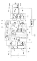
図1は、本発明の好ましい実施態様にかかるスイッチング電源装置の回路図である。
【0059】
図1に示すように、本実施態様にかかるスイッチング電源装置は、一対の入力電源端子41、42に供給される直流入力電圧Vinを降圧して、一対の出力電源端子43、44に直流出力電圧Voutを発生させ、これを負荷に供給する装置であり、入力電源端子41、42に接続されたバックコンバータ回路50と、バックコンバータ回路50に接続されトランスT2の1次巻線Lp11を励磁するハーフブリッジ回路60と、バックコンバータ回路50の動作を制御するバックコンバータ制御回路71と、ハーフブリッジ回路60の動作を制御するハーフブリッジ制御回路72と、通常動作時においてバックコンバータ制御回路71及びハーフブリッジ制御回路72の動作電圧Vccを生成する補助電源回路80と、起動時において上記動作電圧Vccを生成する第1の動作電圧生成回路90と、動作終了時において上記動作電圧Vccを生成する第2の動作電圧生成回路100と、トランスT2の2次側に設けられた自己ドライブ型の整流回路110と、整流回路110の後段に設けられ出力電源端子43、44に接続された平滑回路120とを備える。
【0060】
また、直流入力電源と入力電源端子41との間には、動作スイッチS11が設けられており、スイッチング電源装置による変圧動作を行う場合には、これを外部からオンさせる必要がある。本実施態様においては、動作スイッチS11はスイッチング電源装置の一部を構成する要素ではないが、これをスイッチング電源装置の一部に含めても構わない。
【0061】
バックコンバータ回路50は、メインスイッチQ11、Q12と、平滑リアクトルLbとを備えている。図1に示すように、メインスイッチQ11と平滑リアクトルLbは、高位側の入力電源端子41とハーフブリッジ回路60との間に直列に接続されており、メインスイッチQ12は、低位側の入力電源端子42とメインスイッチQ11及び平滑リアクトルLbの接続点との間に接続されている。バックコンバータ回路50は、バックコンバータ制御回路71による制御のもと、入力電源端子41、42間に現れる直流入力電圧Vinを降圧して一対の内部配線45、46間に内部電圧Vpを発生させる。
【0062】
ハーフブリッジ回路60は、一対の内部配線45、46間に直列に接続されたメインスイッチQ13、Q14と、同じく一対の内部配線45、46間に直列に接続された1次側コンデンサC11、C12とを備えている。図1に示すように、メインスイッチQ13及びQ14の接続点と1次側コンデンサC11及びC12の接続点との間には、トランスT2の1次巻線Lp11が接続されている。
【0063】
バックコンバータ制御回路71は、バックコンバータ回路50を構成するメインスイッチQ11、Q12のスイッチング動作を制御する回路であり、メインスイッチQ11、Q12は、バックコンバータ制御回路71による制御のもと、所定のデッドタイムをはさんで交互にオン状態とされる。バックコンバータ制御回路71は、出力電圧Voutに基づいてメインスイッチQ11のデューティを制御し、より具体的には、バックコンバータ制御回路71は、出力電圧Voutが目標電圧と比べて高くなるほどメインスイッチQ11のデューティを低下させることによって、内部配線45、46を介してハーフブリッジ回路60に供給される電力を減らし、逆に、出力電圧Voutが目標電圧と比べて低くなるほどメインスイッチQ11のデューティを上昇させることによって、ハーフブリッジ回路60に供給される電力を増やす。このようにして、ハーフブリッジ回路60には、直流入力電圧Vin及びメインスイッチQ11のデューティにより決まる一定の内部電圧Vpが与えられる。
【0064】
尚、バックコンバータ制御回路71は1次側回路に属するため、出力電圧Voutを直接受けることはできず、図1に示すように、絶縁回路130を介して出力電圧Voutに連動する電圧Vout’がバックコンバータ制御回路71に与えられる。バックコンバータ制御回路71の最低動作電圧については後述する。
【0065】
ハーフブリッジ制御回路72は、ハーフブリッジ回路60を構成するメインスイッチQ13、Q14のスイッチング動作を制御する回路であり、常に、一定のデューティでこれらを駆動する。これにより、一対の出力電源端子43、44間には、内部電圧Vp及びトランスT2の巻数比により決まる一定の直流出力電圧Voutが現れる。ハーフブリッジ制御回路72の最低動作電圧についても後述する。
【0066】
補助電源回路80は、通常動作時においてバックコンバータ制御回路71及びハーフブリッジ制御回路72の動作電圧を生成する回路であり、ダイオードブリッジ回路Bと、平滑コンデンサC13、C14と、トランジスタTr11と、抵抗R11、R12とを備える。ダイオードブリッジ回路Bは、トランスT2の1次側に設けられた補助巻線Lp12に現れる電圧を整流する回路であり、その出力端間に現れる電圧は、平滑コンデンサC13により平滑されて補助電源電圧Vsubとなる。また、トランジスタTr11は、ダイオードブリッジ回路Bの高位側の出力端とVcc配線との間に設けられており、そのベース−エミッタ間には抵抗R11が設けられている。ダイオードブリッジ回路Bの低位側の出力端は、内部配線46に直接接続されている。かかる構成により、補助電源回路80は、ハーフブリッジ回路60がスイッチング動作を開始すると、補助巻線Lp12に現れる電圧を用いてVcc配線に所定の動作電圧を供給する。ここで、補助電源回路80によりVcc配線に与えられる動作電圧を「Vcc1」と定義する。
【0067】
第1の動作電圧生成回路90は、起動時においてバックコンバータ制御回路71及びハーフブリッジ制御回路72の動作電圧Vccを生成する回路であり、トランジスタTr12と、抵抗R13と、ツェナーダイオードZ11と、ダイオードD11と、動作スイッチS12とを備える。図1に示すように、トランジスタTr12とダイオードD11は、高位側の入力電源端子41とVcc配線との間に直列に接続されており、抵抗R13とツェナーダイオードZ11は、高位側の入力電源端子41と低位側の入力電源端子42との間に直列に接続されている。抵抗R13とツェナーダイオードZ11との接続点は、トランジスタTr12のベースに接続されており、これによりトランジスタTr12のベースには、ツェナーダイオードZ11のツェナー電圧VZ11が与えられる。したがって、トランジスタTr12がオン状態となると、Vcc配線に与えられる電圧は、VZ11−2Vth(Vthは、トランジスタTr12のベース−エミッタ間電圧及びダイオードD11の順方向電圧)となる。このようにして第1の動作電圧生成回路90によりVcc配線に与えられる動作電圧を「Vcc2」と定義する。
【0068】
ここで、本実施態様においては、
Vcc1>Vcc2
となるように、ツェナーダイオードZ11のツェナー電圧VZ11が選択されている。このため、第1の動作電圧生成回路90はスイッチング電源装置の起動時においてのみ動作し、ハーフブリッジ回路60がスイッチング動作を開始するとトランジスタTr12はオフ状態となる。これにより、第1の動作電圧生成回路90は、スイッチング電源装置の動作に実質的に寄与しなくなる。
【0069】
さらに、第1の動作電圧生成回路90に備えられた動作スイッチS12は、ツェナーダイオードZ11の両端間に接続されており、スイッチング電源装置による変圧動作を行う場合には、これを外部からオフさせる必要がある。したがって、本実施態様にかかるスイッチング電源装置を動作させるためには、動作スイッチS11をオン状態とし、動作スイッチS12をオフ状態とする必要がある。逆に、本実施態様にかかるスイッチング電源装置の動作を停止させるためには、動作スイッチS11をオフ状態とするか、動作スイッチS12をオン状態とすればよい。
【0070】
第2の動作電圧生成回路100は、動作終了時においてバックコンバータ制御回路71及びハーフブリッジ制御回路72の動作電圧を生成する回路であり、トランジスタTr13と、トランジスタTr14と、ダイオードD12と、ツェナーダイオードZ12とを備える。トランジスタTr13とダイオードD12は内部配線45とVcc配線との間に直列に接続されており、トランジスタTr14は内部配線45とトランジスタTr13のベースとの間に接続されており、ツェナーダイオードZ12はトランジスタTr13のベースと内部配線46との間に接続されている。トランジスタTr14のゲート−ソース間は短絡されており、これにより定電流素子として機能する。尚、トランジスタTr14の代わりに抵抗を用いても構わない。
【0071】
また、ツェナーダイオードZ12のツェナー電圧VZ12は、ツェナーダイオードZ11のツェナー電圧VZ11よりも低く設定されている。このため、動作スイッチS11がオンであり、動作スイッチS12がオフである状態においては、トランジスタTr12のベース電圧は常にトランジスタTr13のベース電圧はよりも高くなることから、トランジスタTr13のベース−エミッタ間電圧はしきい値電圧未満となり、トランジスタTr13のオフ状態が保たれる。トランジスタTr13がオフ状態である場合においては、第2の動作電圧生成回路100はスイッチング電源装置の動作に実質的に寄与しない。
【0072】
一方、トランジスタTr13がオン状態となると、Vcc配線に与えられる電圧は、VZ12−2Vth(Vthは、トランジスタTr13のベース−エミッタ間電圧及びダイオードD12の順方向電圧)となる。このようにして第2の動作電圧生成回路100によりVcc配線に与えられる動作電圧を「Vcc3」と定義する。
【0073】
上述のとおり、本実施態様においては、ツェナーダイオードZ12のツェナー電圧VZ12がツェナーダイオードZ11のツェナー電圧VZ11よりも低く設定されていることから、
Vcc2>Vcc3
である。このため、第2の動作電圧生成回路100は、動作スイッチS11がオフするか動作スイッチS12がオンすることにより、トランジスタTr12がオフ状態となっている期間においてのみ動作可能となる。
【0074】
ここで、本実施態様においては、バックコンバータ制御回路71の最低動作電圧はVcc2未満、Vcc3以上に設定されており、ハーフブリッジ制御回路72の最低動作電圧はVcc3未満に設定されている。これにより、バックコンバータ制御回路71は、補助電源回路80又は第1の動作電圧生成回路90が活性状態となっている場合には、メインスイッチQ11、Q12の駆動を行うことができる一方、これらが非活性状態となっており、代わりに第2の動作電圧生成回路100が活性状態となっている場合には、メインスイッチQ11、Q12の駆動を行うことができない。一方、ハーフブリッジ制御回路72は、補助電源回路80、第1の動作電圧生成回路90及び第2の動作電圧生成回路100のいずれかが活性状態となっている限り、メインスイッチQ13、Q14の駆動を行うことができる。
【0075】
整流回路110は、整流スイッチQ15、Q16と、抵抗R14、R15とを備える。整流スイッチQ15はトランスT2の2次巻線Ls11と低位側の出力電圧端子44との間に接続されており、整流スイッチQ16はトランスT2の2次巻線Ls12と低位側の出力電圧端子との間に接続されている。また、整流スイッチQ15のゲートは2次巻線Ls12に接続され、整流スイッチQ16のゲートは2次巻線Ls112に接続されている。これにより、整流回路110は、いわゆる自己ドライブ型の整流回路を構成している。さらに、整流スイッチQ15、Q16のゲート−ソース間にはそれぞれ抵抗R14、R15が挿入されており、これによりゲート電極がフローティング状態となることが防止されている。
【0076】
平滑回路120は、整流回路110の整流出力端と高位側の出力電圧端子43との間に接続された出力リアクトルLoutと、一対の出力電圧端子43、44間に接続された出力コンデンサCoutとを備える。
【0077】
そして、本実施態様にかかるスイッチング電源装置の一部を構成する要素ではないが、一対の出力電圧端子43、44間に接続される負荷は、抵抗成分RLoadと容量成分CLoadとリアクトル成分LLoadによって表すことができる。
【0078】
次に、本実施態様にかかるスイッチング電源装置の動作について説明する。
【0079】
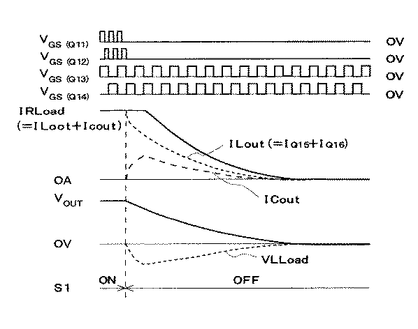
図2は、図1に示すスイッチング電源装置の動作を示すタイミング図である。
【0080】
本実施態様にかかるスイッチング電源装置を動作させるためには、まず、動作スイッチS11を外部からオンさせるとともに、動作スイッチS12を外部からオフさせる必要がある。動作スイッチS11をオン、動作スイッチS12をオフさせると、第1の動作電圧生成回路90内のトランジスタTr12がオンし、Vcc配線に与えられる動作電圧はVcc2となる。
【0081】
これにより、バックコンバータ制御回路71及びハーフブリッジ制御回路72はいずれも動作状態となり、バックコンバータ制御回路71はメインスイッチQ11、Q12を電圧Vout’に基づくデューティにて交互にオン/オフさせ、ハーフブリッジ制御回路72はメインスイッチQ13、Q14をある決まったデューティで交互にオン/オフさせる。
【0082】
これにより、トランスT2の1次側電圧VLp11の極性は交互に反転し、これに連動して、トランスT2の2次巻線Ls11及びLs12に発生する2次側電圧の極性も交互に反転することから、整流スイッチQ15、Q16は交互にオン/オフする。これにより極性が交互に反転する2次側電圧が整流され、平滑回路120によって平滑されて安定した出力電圧Voutが生成される。
【0083】
図3は、図2に示したタイミング図の主要部を拡大してより詳細に示した図である。
【0084】
図3に示すように、メインスイッチQ13、Q14がハーフブリッジ制御回路72の制御によってスイッチング動作を繰り返すと、出力リアクトルLoutに流れる電流ILoutの波形はスイッチング周波数の2倍の周波数を持った波形となり、トランスT2の1次巻線Lp11に流れる電流ILp11の波形はスイッチング周波数と同じ周波数を持った波形となる。この場合、出力リアクトルLoutに流れる電流ILoutの方向が正である場合には出力コンデンサCoutが充電され、負である場合には出力コンデンサCoutが放電されることになる。
【0085】
また、メインスイッチQ13がオンしている期間においては、トランスT2の1次巻線Lp11に流れる電流ILp11の方向が正である場合には1次側コンデンサC11は放電され、負である場合には1次側コンデンサC11は充電されることになる。図3には示されていないが、同様に、メインスイッチQ14がオンしている期間においては、トランスT2の1次巻線Lp11に流れる電流ILp11の方向が正である場合には1次側コンデンサC12は充電され、負である場合には1次側コンデンサC12は放電されることになる。
【0086】
一方、ハーフブリッジ回路60のスイッチング動作によりトランスT2の1次側に設けられた補助巻線Lp12に電圧が発生すると、補助電源回路80によってVcc配線に与えられる動作電圧はVcc1となり、これに伴って第1の動作電圧生成回路90は非活性化される。
【0087】
そして、任意のタイミングにて動作スイッチS12をオンに変化させると、トランジスタTr12のベース電圧が低下し、トランジスタTr12がターンオフする。トランジスタTr12がターンオフすると、トランジスタTr11のベース電圧も低下するので、トランジスタTr11がターンオフする。
【0088】
これによりVcc配線の電位が低下するので、トランジスタTr13のベース−エミッタ間電圧はしきい値電圧を越えてターンオンする。これにより、Vcc配線の電位はVcc3となるので、バックコンバータ制御回路71の動作が停止する。すなわち、メインスイッチQ11、Q12はいずれもオフ状態となる。一方、ハーフブリッジ制御回路72については、最低動作電圧がVcc3未満に設定されていることから、メインスイッチQ13、Q14によるスイッチング動作は継続される。
【0089】
したがって、本実施態様にかかるスイッチング電源装置においては、整流スイッチQ15及びQ16も通常のスイッチング周期にて交互にオン/オフすることになり、従来のスイッチング電源装置のように一方の整流スイッチがオン状態のままとなる現象は生じない。
【0090】
このように、本実施態様によるスイッチング電源装置では、動作スイッチS12のオンにより動作の停止が指示された後においても、メインスイッチQ13、Q14がスイッチング動作を継続することから、出力コンデンサCout及び負荷の容量成分CLoadに蓄積されているエネルギーは、負荷の抵抗成分RLoadやメインスイッチQ13、Q14、並びに、整流スイッチQ15、Q16等により徐々に消費され、これにより出力電圧Voutは低下する。この場合、メインスイッチQ13、Q14は通常のスイッチング周波数で動作を行っていることから、従来のスイッチング電源装置のように出力電圧Voutが大きく振動しながら低下することはなく、実質的に単調に低下することになる。
【0091】
また、動作スイッチS12がオンされた後においてもスイッチング動作が継続されることから、従来のスイッチング電源装置のようにフライバック電圧が発生することはなく、このためスイッチング回路内の内部電圧Vpが押し上げられることもない。スイッチング回路内の内部電圧Vpは図2に示すように単調に低下し、これによりVcc配線の電位がハーフブリッジ制御回路72の最低動作電圧を下回ると、全てのスイッチング動作は停止する。この時点においては、出力コンデンサCout及び負荷の容量成分CLoadに蓄積されているエネルギーの多くは既に消費されていることから、従来のように、スイッチング周期よりも非常に長い周期での発振が生じることはない。
【0092】
さらに、動作スイッチS12がオンされた後におけるスイッチング動作は、通常動作時におけるスイッチング動作と全く同じであることから、出力リアクトルLoutに流れる電流も通常動作時における電流と同じであり、異常な電流が流れることはない。
【0093】
しかも、本実施態様によるスイッチング電源装置では、動作スイッチS12のオンにより動作の停止が指示された後においても、メインスイッチQ13、Q14がスイッチング動作を継続することから、整流スイッチQ15(ボディダイオード)、トランスの2次巻線Ls11、出力リアクトルLout、出力コンデンサCoutからなるLCR直列回路、並びに、整流スイッチQ16(ボディダイオード)、トランスの2次巻線Ls12、出力リアクトルLout、出力コンデンサCoutからなるLCR直列回路が振動し出力電圧Voutにアンダーシュートが発生する条件を次式によって表すことができる。
【0094】
【数3】
【0095】
式(3)から明らかなように、本実施態様によれば、従来のスイッチング電源装置に比べて1次側コンデンサC11、C12の容量が付加される分、LCR直列回路が振動的となりにくいことが分かる。したがって、付加コンデンサCexを用いることなく、1次側コンデンサC11、C12の容量を利用して出力電圧Voutのアンダーシュートを防止することが可能となる。
【0096】
図4は、図2に示したタイミング図の主要部を拡大して示すとともに、負荷の抵抗成分RLoadに流れる電流IRLoadの変化を示す図である。
【0097】
図4に示すように、1次側コンデンサC11、C12の容量の付加によって、式(3)の条件が満たされなくなれば、動作スイッチS12がオンされたことによりリアクトル成分LLoadに電圧(VLLoad)が発生しても、上記LCR直列回路が共振条件を満たしていないことから出力電圧Voutがマイナス側に振れることはない。すなわち、アンダーシュートの発生を防止することが可能となる。
【0098】
このように、本実施態様にかかるスイッチング電源装置によれば、動作スイッチS12をターンオンさせることによって、従来のスイッチング電源装置における種々の問題を生じさせることなく、動作を停止させることができるので、動作スイッチS11をオンしたままの状態で、動作の開始及び停止を行うことが可能となる。したがって、本実施態様は、動作スイッチS11がスイッチング電源装置の外部に配置されている場合において特に好適である。
【0099】
また、本実施態様にかかるスイッチング電源装置によれば、通常動作時においては補助電源回路80がVcc配線に動作電圧を供給し、第1の動作電圧生成回路90が非活性化されることから、動作電圧を生成する際に生じる損失が低減される。
【0100】
さらに、本実施態様にかかるスイッチング電源装置によれば、ハーフブリッジ回路60の前段にバックコンバータ回路50が備えられ、これら2段のコンバータによって降圧を行っていることから、各コンバータにて発生する損失が大幅に低減され、全体としての変換効率が高められる。
【0101】
尚、図2及び図4に示したタイミング図には、動作スイッチS12をターンオンさせることによって動作を停止させた例が示されているが、動作を停止させる方法としてはこれに限らず、動作スイッチS11をターンオフすることによって動作を停止させても構わない。この場合も、動作スイッチS12をターンオンさせた場合と同様、従来のスイッチング電源装置における種々の問題を生じさせることなく、動作を停止させることができる。
【0102】
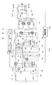
また、上記実施態様スイッチング電源装置においては、第2の動作電圧生成回路100を構成するトランジスタTr13のコレクタ及びトランジスタTr14のドレインがいずれも内部配線45に接続されているが、図5に示すように、これらを補助電源回路80を構成するダイオードブリッジ回路の高位側出力端に接続しても構わない。この場合も、図1に示すスイッチング電源装置とほぼ同じ動作を行うことができる。
【0103】
次に、本発明の好ましい他の実施態様について説明する。
【0104】
図6は、本発明の好ましい他の実施態様にかかるスイッチング電源装置の回路図である。
【0105】
図6に示すように、本実施態様にかかるスイッチング電源装置は、図1に示したスイッチング電源装置に付加回路140を付加した構成を有しており、その他の点は図1に示したスイッチング電源装置と同様の構成を有している。
【0106】
付加回路140は、内部配線45、46間に直列接続された付加コンデンサCa及び付加抵抗Raによって構成され、スイッチング電源装置の動作停止時においてLCR直列回路が振動的となる共振条件を緩和する役割を果たす。本実施態様においては、LCR直列回路が振動的となって出力電圧Voutにアンダーシュートが発生する条件は次式によって表すことができる。
【0107】
【数4】
【0108】
尚、本実施態様は、当然ながら、図5に示すスイッチング電源装置に対しても適用することが可能である。
【0109】
本発明は、以上の実施態様に限定されることなく、特許請求の範囲に記載された発明の範囲内で種々の変更が可能であり、それらも本発明の範囲内に包含されるものであることはいうまでもない。
【0110】
例えば、上記各実施態様にかかるスイッチング電源装置においては、ツェナーダイオードZ12のツェナー電圧VZ12を、ツェナーダイオードZ11のツェナー電圧VZ11よりも低く設定することにより上記動作を実現しているが、動作スイッチS11がオン状態であり、動作スイッチS12がオフ状態である場合にトランジスタTr12のベース電圧がトランジスタTr13のベース電圧よりも高くなるように構成されている限り、例えば、ツェナーダイオードZ11に対して1又は2以上の通常のダイオードを直列に接続すれば、ツェナー電圧VZ11とツェナー電圧VZ12とが同じ電圧であっても構わないし、逆に、ツェナー電圧VZ11の方がツェナー電圧VZ12よりも低くても構わない。
【0111】
また、上記各実施態様にかかるスイッチング電源装置においては、バックコンバータ制御回路71の最低動作電圧をハーフブリッジ制御回路72の最低動作電圧よりも高く設定することにより上記動作を実現しているが、第2の動作電圧生成回路100が活性化した状態においてバックコンバータ制御回路71の動作が停止し、ハーフブリッジ制御回路72の動作が停止しない限り、例えば、Vcc配線とバックコンバータ制御回路71のVcc入力端との間に、1又は2以上のダイオードを直列に接続すれば、これら最低動作電圧が等しくても構わないし、逆に、バックコンバータ制御回路71の最低動作電圧の方がハーフブリッジ制御回路72のそれよりも低くても構わない。
【0112】
さらに、上記各実施態様にかかるスイッチング電源装置においては、トランスT2の1次側回路として、バックコンバータ回路50とハーフブリッジ回路60の直列回路を用いているが、本発明に適用可能な1次側回路としてはこれに限定されず、他のコンバータ回路を直列に用いても構わない。例えば、バックコンバータ回路50の代わりに、ブーストコンバータ回路等の別の回路を用いてもよく、また、ハーフブリッジ回路60の代わりにフォワードコンバータ、フルブリッジ、プッシュプル回路等の別の回路を用いても構わない。
【0113】
また、上記各実施態様にかかるスイッチング電源装置においては、整流回路110として自己ドライブ型の整流回路を用いているが、上述のとおり、スイッチング電源装置の動作停止時に出力電圧Voutにアンダーシュートが生じるという問題は、整流回路が自己ドライブ型であるか否かに関わらず生じる問題であることから、本発明において、自己ドライブ型の整流回路110の代わりに、ダイオードを用いた通常の整流回路や、ドライバによって動作が制御される同期整流型の整流回路を用いても構わない。
【0114】
さらに、上記各実施態様にかかるスイッチング電源装置においては、バックコンバータ制御回路71及びハーフブリッジ制御回路72が1次側回路に属しているが、これらが2次側回路に属するように構成しても構わない。
【0115】
【発明の効果】
以上説明したように、本発明にかかるスイッチング電源装置によれば、動作の停止が指示された際に、出力電圧Voutが大きく振動したりアンダーシュートを起こすことがなく、実質的に単調に低下することから、負荷の誤動作を効果的に防止することが可能となる。また、本発明にかかるスイッチング電源装置によれば、動作の停止が指示された際に、1次側のスイッチング回路内の内部電圧Vpが段階的に上昇することがなく、ゆるやかに低下することから、1次側回路において用いる素子の破壊を効果的に防止することが可能となる。また、耐圧の高い素子を用いる必要がなくなるので、スイッチング電源装置のコストを低減させることもできる。さらに、本発明にかかるスイッチング電源装置によれば、動作の停止が指示された際に、出力リアクトルLoutに大きな電流が流れることがないので、スイッチング電源装置の信頼性を高めることが可能となる。
【0116】
したがって、本発明にかかるスイッチング電源装置は、容量成分CLoadの大きい負荷に電力を供給するためのスイッチング電源装置として特に好適である。また、本発明にかかるスイッチング電源装置は、軽負荷状態となることが多い負荷に電力を供給するためのスイッチング電源装置として特に好適である。さらに、本発明は、サーバのように低電圧・大電流が求められる負荷を駆動するためのスイッチング電源装置としても好適である。すなわち、本発明にかかるスイッチング電源装置によれば、大負荷時に動作の停止が指示された場合であっても、軽負荷時に動作の停止が指示された場合であっても、出力電圧Voutを単調低下させることが可能となる。
【図面の簡単な説明】
【図1】本発明の好ましい実施態様にかかるスイッチング電源装置の回路図である。
【図2】図1に示すスイッチング電源装置の負荷の抵抗成分RLoadが十分に大きい場合の動作を示すタイミング図である。
【図3】図2に示したタイミング図の主要部を拡大してより詳細に示した図である。
【図4】図1に示すスイッチング電源装置の負荷の抵抗成分RLoadが十分に小さい場合の負荷の抵抗成分RLoadに流れる電流IRLoadの変化を示す図である。
【図5】図1に示すスイッチング電源装置の変形例を示す回路図である。
【図6】本発明の好ましい他の実施態様にかかるスイッチング電源装置の回路図である。
【図7】従来のスイッチング電源装置の回路である。
【図8】従来のスイッチング電源装置において、動作停止時に出力電圧が振動する様子を示すタイミング図である。
【図9】従来のスイッチング電源装置において、動作停止時に出力電圧Voutがアンダーシュートする様子を示すタイミング図である。
【符号の説明】
10 制御回路
20 絶縁回路
41,42 入力電源端子
43,44 出力電源端子
45,46 内部配線
50 バックコンバータ回路
60 ハーフブリッジ回路
71 バックコンバータ制御回路
72 ハーフブリッジ制御回路
80 補助電源回路
90 第1の動作電圧生成回路
100 第2の動作電圧生成回路
110 整流回路
120 平滑回路
130 絶縁回路
140 付加回路
T1,T2 トランス
Q1,Q2,Q11〜Q14 メインスイッチ
Q3,Q4,Q15,Q16 整流スイッチ
C1,C2,C11,C12 1次側コンデンサ
C3,C13,C14 平滑コンデンサ
Cout 出力コンデンサ
CLoad 容量成分
Ca 付加コンデンサ
Lp1,Lp11 1次巻線
Lp12 補助巻線
Ls1,Ls2,Ls11,Ls12 2次巻線
Lb 平滑リアクトル
Lout 出力リアクトル
LLoad リアクトル成分
R1〜R3,R11〜R15 抵抗
RLoad 抵抗成分
Ra 付加抵抗
Tr1,Tr11〜Tr14 トランジスタ
Z1,Z11,Z12 ツェナーダイオード
D11,D12 ダイオード
S1,S2,S11,S12 動作スイッチ
B ダイオードブリッジ回路[0001]
BACKGROUND OF THE INVENTION
The present invention relates to a switching power supply device, and more particularly to a switching power supply device in which undershoot and vibration of an output voltage Vout when operation is stopped are prevented.
[0002]
[Prior art]
2. Description of the Related Art Conventionally, a switching power supply device has been widely used as a power supply device for electronic equipment and electrical equipment represented by computers.
[0003]
FIG. 7 is a circuit of a conventional switching power supply device.
[0004]
As shown in FIG. 7, the conventional switching power supply device includes a transformer T1, a half-bridge type switching circuit provided on the primary side of the transformer T1, and a self-drive type provided on the secondary side of the transformer T1. The apparatus includes a rectifier circuit and a smoothing circuit, generates a DC output voltage Vout by stepping down the DC input voltage Vin supplied to the switching circuit on the primary side, and supplies this to a load. As shown in FIG. 7, the load is represented by a resistance component RLoad, a capacitance component CLoad, and a reactor component LLoad.
[0005]
The operations of the main switches Q1 and Q2 constituting the primary side switching circuit are controlled by the
[0006]
The operating voltage Vcc of the
[0007]
On the other hand, the rectifying switches Q3 and Q4 constituting the secondary side rectifier circuit are self-driven by the secondary side voltage of the transformer T1. Also, resistors R2 and R3 are inserted between the gates and sources of the rectifying switches Q3 and Q4, respectively, thereby preventing the gate electrode from being in a floating state.
[0008]
Next, the operation of the conventional switching power supply device shown in FIG. 7 will be described.
[0009]
FIG. 8 is a timing chart showing the operation of the conventional switching power supply device.
[0010]
As shown in FIG. 8, when the operation switch S1 is on, under the control of the
[0011]
In conjunction with this, the polarity of the secondary voltage generated in the secondary windings Ls1 and Ls2 of the transformer T1 is also alternately inverted, whereby the rectifier switches Q3 and Q4 are alternately turned on / off at the switching frequency. To do. More specifically, the gate-source voltage V GS During a period in which the main switch Q1 is on because (Q1) is at a high level, the gate-source voltage V of the rectifying switch Q3 is generated by the secondary side voltage generated in the secondary winding Ls2. GS (Q3) becomes a voltage equal to or higher than the threshold voltage, whereby the rectifying switch Q3 is turned on. Conversely, the gate-source voltage V GS During a period in which the main switch Q2 is on because (Q2) is at a high level, the gate-source voltage V of the rectifier switch Q4 is generated by the secondary side voltage generated in the secondary winding Ls1. GS (Q4) becomes a voltage equal to or higher than the threshold voltage, whereby the rectifying switch Q4 is turned on.
[0012]
As a result, the secondary voltage whose polarity is alternately inverted is rectified and smoothed by the smoothing circuit including the output reactor Lout and the output capacitor Cout to generate a stable output voltage Vout.
[0013]
When the operation switch S1 is changed to OFF at an arbitrary timing, the transistor Tr1 is turned off, so that the operation of the
[0014]
However, when the operation switch S1 is changed to OFF, the operation of the primary side switching circuit stops, so that either one of the rectifying switches Q3 and Q4 remains on, and the output capacitor Cout and the load capacitance component. A reverse current starts to flow from CLoad to the output reactor Lout.
[0015]
FIG. 8 shows a case where the rectification switch Q3 remains in the on state first because the operation switch S1 is turned off. In this case, since the operation of the switching circuit on the primary side is stopped, the discharge route of the charge stored in the gate of the rectifying switch Q3 is substantially only the resistor R2, and between the gate and the source of the rectifying switch Q3. Voltage V GS (Q3) gradually decreases due to the current flowing through the resistor R2. During this time, a reverse current continues to flow through the output reactor Lout.
[0016]
Thereafter, the gate-source voltage V of the rectifier switch Q3 is reduced by the decrease in Vout due to the discharge from the output capacitor Cout and the capacitive component CLoad of the load, the decrease in the secondary voltage of the winding, and the discharge of the gate charge through the resistor R2. GS When (Q3) drops below the threshold voltage and changes to an off state, a flyback voltage is generated in the transformer T1. Such a flyback voltage pushes up the internal voltage Vp in the switching circuit via the transformer T1, and at the same time, the gate-source voltage V of the rectifying switch Q4. GS Jump up (Q4). As a result, the rectification switch Q4 is now kept on.
[0017]
Further, as shown in FIG. 8, since the current flowing through the output reactor Lout through the rectifier switch Q4 is once in the forward direction, the output capacitor Cout and the load capacitance component CLoad are charged during this period, and the output voltage Vout increases. To do.
[0018]
After that, the gate-source voltage V of the rectifier switch Q4 GS (Q4) shows a decrease in Vout due to discharge from the output capacitor Cout and the load capacitance component CLoad, a decrease in the secondary voltage of the winding, and the resistance R3 from the time when the current flowing through the output reactor Lout is reversed. When the current begins to slowly drop due to the flowing current and falls below the threshold voltage and the rectifier switch Q4 changes to the OFF state, a flyback voltage is generated again in the transformer T1, and the internal voltage in the switching circuit is passed through the transformer T1. While pushing up Vp, the gate-source voltage V of the rectifier switch Q3 GS Jump up (Q4). As a result, the rectifying switch Q3 is now kept in the on state.
[0019]
Such an operation is repeated until the output capacitor Cout and the load capacitance component CLoad are consumed by the secondary circuit of the switching power supply device and the load resistance component RLoad, whereby the output voltage Vout The internal voltage Vp in the switching circuit rises stepwise while oscillating with a period much longer than the switching period.
[0020]
[Problems to be solved by the invention]
As described above, in the conventional switching power supply device, even if the operation is stopped, the output voltage Vout does not decrease monotonously, but decreases while oscillating at a cycle longer than the normal switching cycle. May occur. For example, if the output voltage Vout decreases to a predetermined value or less, the load is determined to be stopped and the predetermined operation is performed. When the output voltage Vout decreases while oscillating, the load There arises a problem that it becomes difficult to determine whether or not the operation of the switching power supply has stopped.
[0021]
Further, in the conventional switching power supply device, when the operation is stopped, the internal voltage Vp in the primary side switching circuit increases stepwise, and there is a possibility that elements used in the primary side circuit are destroyed. . In order to prevent this, it is necessary to use an element with a high breakdown voltage, which increases the cost of the switching power supply device.
[0022]
Further, in the conventional switching power supply device, when the operation is stopped, a large current flows through the output reactor Lout on the secondary side, the secondary windings Ls1 and Ls2 of the transformer, and the rectifier switches Q3 and Q4. Therefore, the output reactor Lout, Large heat is generated in the secondary windings Ls1 and Ls2 of the transformer and the rectifying switches Q3 and Q4, and there is a possibility that the reliability of the switching power supply device is lowered.
[0023]
The above-described problem becomes more prominent as the resistance component RLoad of the load is larger. For example, this problem is particularly problematic when the operation of the switching power supply device is stopped at a light load. Furthermore, the above-described problem becomes more problematic as the capacitance component CLoad of the load increases, and is particularly problematic when power is supplied to a load having a large capacitance component CLoad.
[0024]
On the other hand, when the resistance component RLoad of the load is sufficiently small (when the load is large), the above-described problem is relatively difficult to occur, but when the resistance component RLoad is small (when the load is large), the operation of the switching power supply device When the operation is stopped, an undershoot occurs in the output voltage Vout, which may cause a malfunction in the load. If the output voltage Vout becomes a negative voltage, the parasitic diode in the IC included in the load device becomes conductive, and an excessive current flows through the IC. In some cases, the IC may malfunction or be damaged. is there.
[0025]
FIG. 9 is a timing chart showing how the output voltage Vout undershoots when operation is stopped.
[0026]
As shown in FIG. 9, when the operation of the primary side switching circuit is stopped by changing the operation switch S1 to OFF, the current (I) flowing through the resistance component RLoad RLoad ) Is the output current (I) of the output reactor Lout. Lout ) To the discharge current (I Cout ), And the voltage (V) is applied to the reactor component LLoad of the load. LLoad ) Occurs and tries to keep current flowing. As a result, the output voltage Vout fluctuates to the negative side, causing an undershoot. When this undershoot voltage reaches the forward voltage Vf of the body diodes of the rectifying switches Q3 and Q4, these body diodes become conductive, and the rectifying switch Q3 (body diode), the transformer secondary winding Ls1, and the output reactor. Current flows through the LCR series circuit composed of Lout and the output capacitor Cout, and the LCR series circuit composed of the rectifier switch Q4 (body diode), the transformer secondary winding Ls2, the output reactor Lout, and the output capacitor Cout. For this reason, the peak value of the undershoot voltage is clamped to approximately −Vf.
[0027]
Here, when the resistance component RLoad, the reactor component LLoad, and the output capacitor Cout satisfy the following expression, the LCR series circuit becomes oscillating and the above-described undershoot occurs.
[0028]
[Expression 1]
[0029]
[Expression 2]
[0030]
As described above, in the conventional switching power supply device, there is a problem that when the operation stop is instructed, the output voltage Vout decreases while oscillating or an undershoot occurs in the output voltage Vout, and the former problem is the resistance of the load. The larger the component RLoad, the more prominent, and the latter problem becomes more prominent as the resistance component RLoad is smaller. In particular, the latter problem occurs regardless of whether or not the rectifier circuit is a self-drive type.
[0031]
Therefore, an object of the present invention is to provide a switching power supply device in which an undershoot does not occur in the output voltage Vout when an instruction to stop the operation is given.
[0032]
Another object of the present invention is to provide a switching power supply device in which the output voltage Vout does not vibrate greatly when an instruction to stop the operation is given.
[0033]
Still another object of the present invention is to provide a switching power supply apparatus in which the internal voltage Vp in the primary side switching circuit does not increase stepwise when an instruction to stop the operation is given. .
[0034]
Still another object of the present invention is to provide a switching power supply in which a large current does not flow through the output reactor Lout, the secondary windings Ls1 and Ls2 of the transformer, and the rectifying switches Q3 and Q4 when an instruction to stop the operation is given. Is to provide a device.
[0035]
[Means for Solving the Problems]
Such an object of the present invention is connected between the transformer, the input power supply terminal and the primary winding of the transformer. By a first converter and a half bridge, a forward converter, a full bridge or a push-pull circuit constituted by at least a buck converter or a boost converter circuit connected in series between the input power supply terminal and the primary winding of the transformer Consists of a configured second converter Connected to the switching circuit and the secondary winding of the transformer Self-driven A rectifier circuit; a control circuit that controls the operation of the switching circuit; and first and second operation voltage generation circuits that generate an operation voltage of the control circuit; The control circuit includes at least a first converter control circuit that controls the operation of the first converter and a second converter control circuit that controls the operation of the second converter, and the first operating voltage generation circuit includes Supplying the first operating voltage to an operating power supply line provided in common to the first converter control circuit and the second converter control circuit, and the second operating voltage generating circuit is configured to supply the operating power supply. The second operating voltage is supplied to the wiring, and the third operating voltage is applied to the operating power supply wiring using the voltage appearing in the auxiliary winding provided on the primary side of the transformer. An auxiliary power supply circuit for supplying, and when the first operating voltage generating circuit is in an active state, the first converter control circuit and the second converter control circuit are in an operating state; When the second operating voltage generation circuit is in an active state, the operation of the first converter control circuit is stopped, the minimum operating voltage Vcc1 of the auxiliary power supply circuit, the first converter control circuit The minimum operating voltage Vcc2 and the minimum operating voltage Vcc3 of the second converter control circuit have a relationship of Vcc1>Vcc2> Vcc3. This is achieved by the switching power supply device.
[0036]
In a preferred embodiment of the present invention, the first operating voltage generating circuit includes a first Zener diode that determines the first operating voltage, and the second operating voltage generating circuit includes the second operating voltage generating circuit. A second Zener diode for determining the operating voltage is included, the Zener voltage of the first Zener diode; But The zener voltage of the second zener diode Higher than .
[0037]
In a further preferred aspect of the present invention, the first operating voltage generation circuit further includes an operation switch connected in parallel to the first Zener diode.
[0046]
As described above, according to the present invention, the first operating voltage generated by the first operating voltage generating circuit and the second operating voltage generated by the second operating voltage generating circuit are different from each other. In normal operation, the control circuit is operated with the operating voltage of one operating voltage generation circuit, and at the end of operation, the control circuit is operated with the operating voltage of the other operating voltage generation circuit. The switching operation can be continued. As a result, the output voltage can be reduced substantially monotonously without causing vibrations or undershoots, so that malfunction of the load can be effectively prevented.
[0047]
In particular, when the rectifier circuit is a self-drive type rectifier circuit, when an instruction to stop the operation is given, the internal voltage in the switching circuit on the primary side is prevented from being increased stepwise. It becomes possible to effectively prevent destruction of elements used in the secondary circuit. In addition, since it is not necessary to use an element with a high breakdown voltage, the cost of the switching power supply device can be reduced. Furthermore, when an instruction to stop the operation is given, a large current does not flow through the output reactor, the secondary winding of the transformer, and the rectifier circuit, so that reliability can be improved.
[0048]
Therefore, the switching power supply device according to the present invention is particularly suitable as a switching power supply device for supplying power to a load having a large capacitance component CLoad. The switching power supply according to the present invention is particularly suitable as a switching power supply for supplying electric power to a load that is often in a light load state. Furthermore, the present invention is also suitable as a switching power supply device for driving a load that requires a low voltage and a large current, such as a server. That is, according to the switching power supply device according to the present invention, the output voltage is monotonously reduced even when the operation stop is instructed at a heavy load or the operation stop is instructed at a light load. It becomes possible to make it.
[0057]
DETAILED DESCRIPTION OF THE INVENTION
Hereinafter, preferred embodiments of the present invention will be described in detail with reference to the accompanying drawings.
[0058]
FIG. 1 is a circuit diagram of a switching power supply device according to a preferred embodiment of the present invention.
[0059]
As shown in FIG. 1, the switching power supply according to the present embodiment steps down the DC input voltage Vin supplied to the pair of input
[0060]
In addition, an operation switch S11 is provided between the DC input power supply and the input
[0061]
The
[0062]
The half-
[0063]
The buck converter control circuit 71 is a circuit that controls the switching operation of the main switches Q11 and Q12 constituting the
[0064]
Note that since the buck converter control circuit 71 belongs to the primary circuit, it cannot directly receive the output voltage Vout. As shown in FIG. 1, the voltage Vout ′ linked to the output voltage Vout via the insulating
[0065]
The half-
[0066]
The auxiliary
[0067]
The first operating
[0068]
Here, in this embodiment,
Vcc1> Vcc2
Zener voltage V of zener diode Z11 so that Z11 Is selected. Therefore, the first operating
[0069]
Further, the operation switch S12 provided in the first operating
[0070]
The second operating
[0071]
Also, the Zener voltage V of the Zener diode Z12 Z12 Is the Zener voltage V of the Zener diode Z11. Z11 Is set lower. Therefore, when the operation switch S11 is on and the operation switch S12 is off, the base voltage of the transistor Tr12 is always higher than the base voltage of the transistor Tr13. Becomes less than the threshold voltage, and the transistor Tr13 is kept off. When the transistor Tr13 is in the off state, the second operating
[0072]
On the other hand, when the transistor Tr13 is turned on, the voltage applied to the Vcc wiring is V Z12 −2Vth (Vth is the base-emitter voltage of the transistor Tr13 and the forward voltage of the diode D12). Thus, the operating voltage applied to the Vcc wiring by the second operating
[0073]
As described above, in this embodiment, the Zener voltage V of the Zener diode Z12 Z12 Is the Zener voltage V of the Zener diode Z11. Z11 Because it is set lower than
Vcc2> Vcc3
It is. For this reason, the second operating
[0074]
Here, in this embodiment, the minimum operating voltage of the buck converter control circuit 71 is set to less than Vcc2 and Vcc3 or more, and the minimum operating voltage of the half
[0075]
The
[0076]
The smoothing
[0077]
And although it is not an element which comprises a part of switching power supply device concerning this embodiment, the load connected between a pair of
[0078]
Next, the operation of the switching power supply device according to this embodiment will be described.
[0079]
FIG. 2 is a timing chart showing the operation of the switching power supply device shown in FIG.
[0080]
In order to operate the switching power supply device according to this embodiment, first, the operation switch S11 needs to be turned on from the outside and the operation switch S12 needs to be turned off from the outside. When the operation switch S11 is turned on and the operation switch S12 is turned off, the transistor Tr12 in the first operation
[0081]
As a result, the buck converter control circuit 71 and the half
[0082]
As a result, the primary side voltage V of the transformer T2 Lp11 The polarity of the inverting switches Q15 and Q16 are alternately turned on, since the polarity of the secondary side voltage generated in the secondary windings Ls11 and Ls12 of the transformer T2 is also alternately reversed. / Turn off. As a result, the secondary side voltage whose polarity is alternately inverted is rectified and smoothed by the smoothing
[0083]
FIG. 3 is an enlarged view showing the main part of the timing diagram shown in FIG. 2 in more detail.
[0084]
As shown in FIG. 3, when the main switches Q13 and Q14 repeat the switching operation under the control of the half
[0085]
Further, during the period in which the main switch Q13 is on, the current I flowing through the primary winding Lp11 of the transformer T2 Lp11 When the direction is positive, the primary side capacitor C11 is discharged. When the direction is negative, the primary side capacitor C11 is charged. Although not shown in FIG. 3, similarly, during the period in which the main switch Q14 is on, the current I flowing through the primary winding Lp11 of the transformer T2 Lp11 When the direction is positive, the primary side capacitor C12 is charged, and when the direction is negative, the primary side capacitor C12 is discharged.
[0086]
On the other hand, when a voltage is generated in the auxiliary winding Lp12 provided on the primary side of the transformer T2 by the switching operation of the
[0087]
When the operation switch S12 is turned on at an arbitrary timing, the base voltage of the transistor Tr12 decreases and the transistor Tr12 is turned off. When the transistor Tr12 is turned off, the base voltage of the transistor Tr11 is also lowered, so that the transistor Tr11 is turned off.
[0088]
As a result, the potential of the Vcc wiring is lowered, so that the base-emitter voltage of the transistor Tr13 is turned on exceeding the threshold voltage. As a result, the potential of the Vcc line becomes Vcc3, and the operation of the buck converter control circuit 71 is stopped. That is, the main switches Q11 and Q12 are both turned off. On the other hand, for the half
[0089]
Therefore, in the switching power supply device according to this embodiment, the rectifier switches Q15 and Q16 are also turned on / off alternately in the normal switching cycle, and one rectifier switch is in the on state as in the conventional switching power supply device. The phenomenon that remains is not generated.
[0090]
As described above, in the switching power supply according to this embodiment, the main switches Q13 and Q14 continue the switching operation even after the operation stop is instructed by turning on the operation switch S12. The energy accumulated in the capacitance component CLoad is gradually consumed by the load resistance component RLoad, the main switches Q13 and Q14, the rectifier switches Q15 and Q16, and the output voltage Vout is thereby lowered. In this case, since the main switches Q13 and Q14 operate at a normal switching frequency, the output voltage Vout does not decrease while oscillating greatly unlike the conventional switching power supply device, and decreases substantially monotonously. Will do.
[0091]
Further, since the switching operation is continued even after the operation switch S12 is turned on, the flyback voltage is not generated unlike the conventional switching power supply device, and therefore the internal voltage Vp in the switching circuit is pushed up. It will never be done. The internal voltage Vp in the switching circuit decreases monotonously as shown in FIG. 2, and when the potential of the Vcc wiring falls below the minimum operating voltage of the half
[0092]
Further, since the switching operation after the operation switch S12 is turned on is exactly the same as the switching operation in the normal operation, the current flowing through the output reactor Lout is the same as the current in the normal operation, and an abnormal current is generated. There is no flow.
[0093]
Moreover, in the switching power supply device according to the present embodiment, the main switches Q13 and Q14 continue the switching operation even after the operation stop is instructed by turning on the operation switch S12, so that the rectifying switch Q15 (body diode), An LCR series circuit comprising a transformer secondary winding Ls11, an output reactor Lout, and an output capacitor Cout, and an LCR series comprising a rectifier switch Q16 (body diode), a transformer secondary winding Ls12, an output reactor Lout, and an output capacitor Cout. Conditions under which the circuit oscillates and undershoot occurs in the output voltage Vout can be expressed by the following equation.
[0094]
[Equation 3]
[0095]
As apparent from the equation (3), according to the present embodiment, the LCR series circuit is less likely to be oscillating as much as the capacitances of the primary side capacitors C11 and C12 are added compared to the conventional switching power supply device. I understand. Therefore, undershoot of the output voltage Vout can be prevented by using the capacitances of the primary side capacitors C11 and C12 without using the additional capacitor Cex.
[0096]
4 is an enlarged view of the main part of the timing diagram shown in FIG. 2, and the current I flowing through the resistance component RLoad of the load. RLoad It is a figure which shows the change of.
[0097]
As shown in FIG. 4, if the condition of the expression (3) is not satisfied by adding the capacitances of the primary side capacitors C11 and C12, the voltage (V) is applied to the reactor component LLoad when the operation switch S12 is turned on. LLoad ), The output voltage Vout does not swing to the negative side because the LCR series circuit does not satisfy the resonance condition. That is, it is possible to prevent the occurrence of undershoot.
[0098]
As described above, according to the switching power supply device according to the present embodiment, the operation can be stopped without causing various problems in the conventional switching power supply device by turning on the operation switch S12. It is possible to start and stop the operation with the switch S11 kept on. Therefore, this embodiment is particularly suitable when the operation switch S11 is disposed outside the switching power supply device.
[0099]
Further, according to the switching power supply device according to the present embodiment, the auxiliary
[0100]
Furthermore, according to the switching power supply apparatus according to the present embodiment, the
[0101]
2 and 4 show an example in which the operation is stopped by turning on the operation switch S12. However, the method for stopping the operation is not limited to this, and the operation switch is not limited thereto. The operation may be stopped by turning off S11. Also in this case, similarly to the case where the operation switch S12 is turned on, the operation can be stopped without causing various problems in the conventional switching power supply device.
[0102]
In the above-described switching power supply device, the collector of the transistor Tr13 and the drain of the transistor Tr14 that constitute the second operating
[0103]
Next, another preferred embodiment of the present invention will be described.
[0104]
FIG. 6 is a circuit diagram of a switching power supply device according to another preferred embodiment of the present invention.
[0105]
As shown in FIG. 6, the switching power supply according to this embodiment has a configuration in which an
[0106]
The
[0107]
[Expression 4]
[0108]
Needless to say, this embodiment can also be applied to the switching power supply device shown in FIG.
[0109]
The present invention is not limited to the above-described embodiments, and various modifications are possible within the scope of the invention described in the claims, and these are also included in the scope of the present invention. Needless to say.
[0110]
For example, in the switching power supply according to each of the above embodiments, the Zener voltage V of the Zener diode Z12 Z12 Zener voltage V of zener diode Z11 Z11 However, when the operation switch S11 is in the on state and the operation switch S12 is in the off state, the base voltage of the transistor Tr12 becomes higher than the base voltage of the transistor Tr13. For example, if one or more ordinary diodes are connected in series to the Zener diode Z11, the Zener voltage V Z11 And Zener voltage V Z12 May be the same voltage, and conversely, the Zener voltage V Z11 Is the zener voltage V Z12 It may be lower.
[0111]
In the switching power supply according to each of the above embodiments, the above operation is realized by setting the minimum operating voltage of the buck converter control circuit 71 higher than the minimum operating voltage of the half
[0112]
Furthermore, in the switching power supply device according to each of the above embodiments, the series circuit of the
[0113]
In the switching power supply device according to each of the above embodiments, a self-drive rectifier circuit is used as the
[0114]
Further, in the switching power supply device according to each of the above embodiments, the buck converter control circuit 71 and the half
[0115]
【The invention's effect】
As described above, according to the switching power supply device according to the present invention, when the stop of the operation is instructed, the output voltage Vout does not vibrate greatly or causes an undershoot, and substantially decreases monotonously. Therefore, it is possible to effectively prevent a load malfunction. Further, according to the switching power supply device of the present invention, when the operation stop is instructed, the internal voltage Vp in the primary side switching circuit does not increase stepwise but gradually decreases. It becomes possible to effectively prevent destruction of elements used in the primary side circuit. In addition, since it is not necessary to use an element with a high breakdown voltage, the cost of the switching power supply device can be reduced. Furthermore, according to the switching power supply device according to the present invention, when the operation stop is instructed, a large current does not flow through the output reactor Lout, so that the reliability of the switching power supply device can be improved.
[0116]
Therefore, the switching power supply device according to the present invention is particularly suitable as a switching power supply device for supplying power to a load having a large capacitance component CLoad. The switching power supply according to the present invention is particularly suitable as a switching power supply for supplying electric power to a load that is often in a light load state. Furthermore, the present invention is also suitable as a switching power supply device for driving a load that requires a low voltage and a large current, such as a server. That is, according to the switching power supply device of the present invention, the output voltage Vout is monotonously controlled even when the operation stop is instructed at a heavy load or the operation stop is instructed at a light load. It can be reduced.
[Brief description of the drawings]
FIG. 1 is a circuit diagram of a switching power supply device according to a preferred embodiment of the present invention.
FIG. 2 is a timing chart showing an operation when a resistance component RLoad of a load of the switching power supply device shown in FIG. 1 is sufficiently large.
FIG. 3 is an enlarged view showing a main part of the timing diagram shown in FIG. 2 in more detail.
4 is a diagram showing a current I flowing through a load resistance component RLoad when the load resistance component RLoad of the switching power supply device shown in FIG. 1 is sufficiently small. RLoad It is a figure which shows the change of.
FIG. 5 is a circuit diagram showing a modification of the switching power supply device shown in FIG. 1;
FIG. 6 is a circuit diagram of a switching power supply device according to another preferred embodiment of the present invention.
FIG. 7 is a circuit of a conventional switching power supply device.
FIG. 8 is a timing diagram illustrating how the output voltage oscillates when operation is stopped in a conventional switching power supply device;
FIG. 9 is a timing diagram illustrating how the output voltage Vout undershoots when operation is stopped in a conventional switching power supply device;
[Explanation of symbols]
10 Control circuit
20 Insulation circuit
41, 42 Input power supply terminal
43,44 Output power terminal
45, 46 Internal wiring
50 Buck converter circuit
60 half-bridge circuit
71 Buck converter control circuit
72 Half-bridge control circuit
80 Auxiliary power circuit
90 First operating voltage generation circuit
100 Second operating voltage generation circuit
110 Rectifier circuit
120 Smoothing circuit
130 Insulation circuit
140 Additional circuit
T1, T2 transformer
Q1, Q2, Q11 to Q14 Main switch
Q3, Q4, Q15, Q16 Rectifier switch
C1, C2, C11, C12 Primary side capacitor
C3, C13, C14 Smoothing capacitor
Cout output capacitor
CLoad capacitance component
Ca addition capacitor
Lp1, Lp11 primary winding
Lp12 Auxiliary winding
Ls1, Ls2, Ls11, Ls12 Secondary winding
Lb Smooth reactor
Lout output reactor
LLoad reactor component
R1-R3, R11-R15 resistance
RLoad resistance component
Ra additional resistance
Tr1, Tr11 to Tr14 transistors
Z1, Z11, Z12 Zener diode
D11, D12 Diode
S1, S2, S11, S12 Operation switch
B Diode bridge circuit
Claims (3)
Priority Applications (3)
| Application Number | Priority Date | Filing Date | Title |
|---|---|---|---|
| JP2002006995A JP3816396B2 (en) | 2001-12-05 | 2002-01-16 | Switching power supply |
| US10/304,783 US6781852B2 (en) | 2001-12-05 | 2002-11-26 | Switching power supply using a transformer, rectifier, control circuit and voltage generating circuits |
| CNB021559074A CN1264271C (en) | 2001-12-05 | 2002-12-05 | Switch supply source |
Applications Claiming Priority (3)
| Application Number | Priority Date | Filing Date | Title |
|---|---|---|---|
| JP2001370818 | 2001-12-05 | ||
| JP2001-370818 | 2001-12-05 | ||
| JP2002006995A JP3816396B2 (en) | 2001-12-05 | 2002-01-16 | Switching power supply |
Publications (2)
| Publication Number | Publication Date |
|---|---|
| JP2003235256A JP2003235256A (en) | 2003-08-22 |
| JP3816396B2 true JP3816396B2 (en) | 2006-08-30 |
Family
ID=26624878
Family Applications (1)
| Application Number | Title | Priority Date | Filing Date |
|---|---|---|---|
| JP2002006995A Expired - Fee Related JP3816396B2 (en) | 2001-12-05 | 2002-01-16 | Switching power supply |
Country Status (3)
| Country | Link |
|---|---|
| US (1) | US6781852B2 (en) |
| JP (1) | JP3816396B2 (en) |
| CN (1) | CN1264271C (en) |
Cited By (1)
| Publication number | Priority date | Publication date | Assignee | Title |
|---|---|---|---|---|
| US8038646B2 (en) | 2004-10-15 | 2011-10-18 | Olympus Corporation | Body-insertable apparatus and manufacturing method thereof |
Families Citing this family (19)
| Publication number | Priority date | Publication date | Assignee | Title |
|---|---|---|---|---|
| AT504245B1 (en) * | 2003-08-05 | 2009-02-15 | Siemens Ag Oesterreich | SWITCHING REGULATOR |
| US7362598B2 (en) * | 2004-12-17 | 2008-04-22 | Artesyn Technologies, Inc. | Synchronous rectifier gate drive shutdown circuit |
| JP4872254B2 (en) * | 2005-07-11 | 2012-02-08 | ブラザー工業株式会社 | Power supply device and power adjustment method |
| US7425834B2 (en) | 2005-08-26 | 2008-09-16 | Power Integrations, Inc. | Method and apparatus to select a parameter/mode based on a time measurement |
| US7568117B1 (en) | 2005-10-03 | 2009-07-28 | Zilker Labs, Inc. | Adaptive thresholding technique for power supplies during margining events |
| US20070114981A1 (en) * | 2005-11-21 | 2007-05-24 | Square D Company | Switching power supply system with pre-regulator for circuit or personnel protection devices |
| US7511976B2 (en) * | 2006-06-27 | 2009-03-31 | Rockwell Automation Technologies, Inc. | Self powered supply for power converter switch driver |
| FR2928058B1 (en) * | 2008-02-21 | 2010-02-19 | Schneider Toshiba Inverter | SPEED DRIVE INCLUDING A DEVICE FOR PROTECTION AGAINST OVERCURRENTS AND OVERVOLTAGES. |
| US8116106B2 (en) * | 2008-09-19 | 2012-02-14 | Power Integrations, Inc. | Method and apparatus to select a parameter/mode based on a measurement during an initialization period |
| US7965526B2 (en) * | 2009-04-15 | 2011-06-21 | Rockwell Automation Technologies, Inc. | Self powered supply for power converter switch driver |
| JP5223874B2 (en) * | 2010-03-09 | 2013-06-26 | 株式会社村田製作所 | Isolated switching power supply |
| US8476859B2 (en) | 2010-09-30 | 2013-07-02 | Rockwell Automation Technologies, Inc. | DC power for SGCT devices using a high frequency current loop with multiple current transformers |
| EP2429071A4 (en) * | 2010-11-01 | 2013-10-23 | Arkady Anatolievich Stepanov | AUTONOMOUS POWER SOURCE WITH CHARGING FUNCTION USING AN ACCUMULATOR |
| EP2720341B1 (en) * | 2012-10-12 | 2021-04-07 | Samsung Electronics Co., Ltd | Wireless Electric Power Receiver for Wirelessly Regulating Electric Power Using Switch |
| US9407156B2 (en) * | 2013-05-10 | 2016-08-02 | Bose Corporation | Managing leakage inductance in a power supply |
| US9595872B2 (en) | 2014-10-22 | 2017-03-14 | Bose Corporation | Adjustment of circuit operations in response to AC line distortion |
| CN107809184A (en) | 2017-11-29 | 2018-03-16 | 苏州博思得电气有限公司 | A kind of pulse voltage generating means, method and controller |
| CN109956014A (en) * | 2017-12-22 | 2019-07-02 | 中国科学院沈阳自动化研究所 | A power distribution unit for remotely operated submersibles |
| US11139746B2 (en) | 2019-01-31 | 2021-10-05 | Rockwell Automation Technologies, Inc. | Power converter with reduced switch mode power supply EMI |
Family Cites Families (9)
| Publication number | Priority date | Publication date | Assignee | Title |
|---|---|---|---|---|
| US4533986A (en) * | 1983-10-31 | 1985-08-06 | General Electric Company | Compact electrical power supply for signal processing applications |
| GB2179477B (en) * | 1985-08-23 | 1989-03-30 | Ferranti Plc | Power supply circuit |
| EP0741447A3 (en) * | 1995-05-04 | 1997-04-16 | At & T Corp | Circuit and method for controlling a synchronous recifier converter |
| US5870299A (en) * | 1997-05-28 | 1999-02-09 | Lucent Technologies Inc. | Method and apparatus for damping ringing in self-driven synchronous rectifiers |
| JP4210804B2 (en) | 1998-05-26 | 2009-01-21 | サンケン電気株式会社 | Synchronous rectification type DC-DC converter |
| JP3130897B2 (en) | 1999-06-14 | 2001-01-31 | 甲府日本電気株式会社 | Synchronous rectifier converter |
| TWI238592B (en) * | 2000-11-27 | 2005-08-21 | Hon Hai Prec Ind Co Ltd | DC power source converter |
| US6504735B2 (en) * | 2001-03-12 | 2003-01-07 | 02 Micro International Ltd. | Regulated voltage reducing high-voltage isolated DC/DC converter system |
| US6650552B2 (en) * | 2001-05-25 | 2003-11-18 | Tdk Corporation | Switching power supply unit with series connected converter circuits |
-
2002
- 2002-01-16 JP JP2002006995A patent/JP3816396B2/en not_active Expired - Fee Related
- 2002-11-26 US US10/304,783 patent/US6781852B2/en not_active Expired - Fee Related
- 2002-12-05 CN CNB021559074A patent/CN1264271C/en not_active Expired - Fee Related
Cited By (1)
| Publication number | Priority date | Publication date | Assignee | Title |
|---|---|---|---|---|
| US8038646B2 (en) | 2004-10-15 | 2011-10-18 | Olympus Corporation | Body-insertable apparatus and manufacturing method thereof |
Also Published As
| Publication number | Publication date |
|---|---|
| CN1264271C (en) | 2006-07-12 |
| JP2003235256A (en) | 2003-08-22 |
| CN1424812A (en) | 2003-06-18 |
| US20030103360A1 (en) | 2003-06-05 |
| US6781852B2 (en) | 2004-08-24 |
Similar Documents
| Publication | Publication Date | Title |
|---|---|---|
| JP3816396B2 (en) | Switching power supply | |
| JP3861220B2 (en) | DC-DC converter | |
| JP3707409B2 (en) | Switching power supply | |
| JP5085397B2 (en) | Power supply device and semiconductor integrated circuit device | |
| CN105391298B (en) | Dc-dc converter control | |
| JP2003189602A (en) | Dc-dc converter and electric equipment using the same | |
| CN103595253A (en) | Novel control method to reduce switching loss on MOSFET | |
| JP2004173460A (en) | Control method of DC-DC converter, DC-DC converter, semiconductor integrated circuit device, and electronic device | |
| JPWO2000079674A1 (en) | Switching Power Supply | |
| JP3358588B2 (en) | Switching power supply circuit | |
| CN113746341A (en) | Switching converter, method of operation, and controller circuit | |
| JP2006129548A (en) | Power converter | |
| JP3711555B2 (en) | DC / DC converter | |
| JP2006014559A (en) | Dc/dc converter | |
| CN214101190U (en) | electronic circuit device | |
| JP2007185072A (en) | Dc-dc converter | |
| JP2002078325A (en) | Dc-dc converter and electronic apparatus using the same | |
| US20060279968A1 (en) | DC/AC converter circuit and DC/AC conversion method | |
| JPH1118426A (en) | Switching power supply circuit | |
| WO2023243321A1 (en) | Converter device | |
| JP4321277B2 (en) | Power supply | |
| US20220271670A1 (en) | Converter with hold-up circuit and inrush-control circuit | |
| JP3694292B2 (en) | Synchronous rectification type DC-DC converter | |
| JP4997984B2 (en) | Synchronous rectification type DC-DC converter. | |
| KR20020033506A (en) | DC―DC Convertor and an electronic device using the same |
Legal Events
| Date | Code | Title | Description |
|---|---|---|---|
| A621 | Written request for application examination |
Free format text: JAPANESE INTERMEDIATE CODE: A621 Effective date: 20040810 |
|
| A977 | Report on retrieval |
Free format text: JAPANESE INTERMEDIATE CODE: A971007 Effective date: 20051227 |
|
| A131 | Notification of reasons for refusal |
Free format text: JAPANESE INTERMEDIATE CODE: A131 Effective date: 20060131 |
|
| A521 | Request for written amendment filed |
Free format text: JAPANESE INTERMEDIATE CODE: A523 Effective date: 20060323 |
|
| TRDD | Decision of grant or rejection written | ||
| A01 | Written decision to grant a patent or to grant a registration (utility model) |
Free format text: JAPANESE INTERMEDIATE CODE: A01 Effective date: 20060516 |
|
| A61 | First payment of annual fees (during grant procedure) |
Free format text: JAPANESE INTERMEDIATE CODE: A61 Effective date: 20060607 |
|
| R150 | Certificate of patent or registration of utility model |
Free format text: JAPANESE INTERMEDIATE CODE: R150 |
|
| FPAY | Renewal fee payment (event date is renewal date of database) |
Free format text: PAYMENT UNTIL: 20090616 Year of fee payment: 3 |
|
| FPAY | Renewal fee payment (event date is renewal date of database) |
Free format text: PAYMENT UNTIL: 20100616 Year of fee payment: 4 |
|
| FPAY | Renewal fee payment (event date is renewal date of database) |
Free format text: PAYMENT UNTIL: 20110616 Year of fee payment: 5 |
|
| LAPS | Cancellation because of no payment of annual fees |