JP3813614B2 - Error correction circuit and A / D converter - Google Patents
Error correction circuit and A / D converter Download PDFInfo
- Publication number
- JP3813614B2 JP3813614B2 JP2004020922A JP2004020922A JP3813614B2 JP 3813614 B2 JP3813614 B2 JP 3813614B2 JP 2004020922 A JP2004020922 A JP 2004020922A JP 2004020922 A JP2004020922 A JP 2004020922A JP 3813614 B2 JP3813614 B2 JP 3813614B2
- Authority
- JP
- Japan
- Prior art keywords
- circuit
- folding
- output
- converter
- bits
- Prior art date
- Legal status (The legal status is an assumption and is not a legal conclusion. Google has not performed a legal analysis and makes no representation as to the accuracy of the status listed.)
- Expired - Lifetime
Links
- 238000006243 chemical reaction Methods 0.000 claims description 66
- 238000010586 diagram Methods 0.000 description 9
- 238000001514 detection method Methods 0.000 description 2
- 102100028918 Catenin alpha-3 Human genes 0.000 description 1
- 101000916179 Homo sapiens Catenin alpha-3 Proteins 0.000 description 1
- 238000004891 communication Methods 0.000 description 1
- 230000006866 deterioration Effects 0.000 description 1
- 238000005516 engineering process Methods 0.000 description 1
- 238000000034 method Methods 0.000 description 1
- 238000012986 modification Methods 0.000 description 1
- 230000004048 modification Effects 0.000 description 1
Images


Classifications
-
- H—ELECTRICITY
- H03—ELECTRONIC CIRCUITRY
- H03M—CODING; DECODING; CODE CONVERSION IN GENERAL
- H03M1/00—Analogue/digital conversion; Digital/analogue conversion
- H03M1/06—Continuously compensating for, or preventing, undesired influence of physical parameters
-
- H—ELECTRICITY
- H03—ELECTRONIC CIRCUITRY
- H03M—CODING; DECODING; CODE CONVERSION IN GENERAL
- H03M1/00—Analogue/digital conversion; Digital/analogue conversion
- H03M1/06—Continuously compensating for, or preventing, undesired influence of physical parameters
- H03M1/0617—Continuously compensating for, or preventing, undesired influence of physical parameters characterised by the use of methods or means not specific to a particular type of detrimental influence
- H03M1/0634—Continuously compensating for, or preventing, undesired influence of physical parameters characterised by the use of methods or means not specific to a particular type of detrimental influence by averaging out the errors, e.g. using sliding scale
- H03M1/0636—Continuously compensating for, or preventing, undesired influence of physical parameters characterised by the use of methods or means not specific to a particular type of detrimental influence by averaging out the errors, e.g. using sliding scale in the amplitude domain
-
- H—ELECTRICITY
- H03—ELECTRONIC CIRCUITRY
- H03M—CODING; DECODING; CODE CONVERSION IN GENERAL
- H03M1/00—Analogue/digital conversion; Digital/analogue conversion
- H03M1/12—Analogue/digital converters
- H03M1/34—Analogue value compared with reference values
- H03M1/36—Analogue value compared with reference values simultaneously only, i.e. parallel type
- H03M1/368—Analogue value compared with reference values simultaneously only, i.e. parallel type having a single comparator per bit, e.g. of the folding type
Description
本発明は、フォールディング型のA/D(アナログ/デジタル)コンバータ(以下、ADCという)およびこのフォールディング型ADCで用いられるエラー補正回路に関するものである。 The present invention relates to a folding A / D (analog / digital) converter (hereinafter referred to as ADC) and an error correction circuit used in the folding ADC.
フォールディング型ADCは、非特許文献1に記載されているように、フォールディング技術を利用してアナログ/デジタル変換を行うものである。図6に示すように、フォールディング型ADC30は、上位ビット変換用の上位ADC回路32と、下位ビット変換用のフォールディング回路34および下位ADC回路36とを備えている。ここで、上位ADC回路32および下位ADC回路36としては、例えば並列比較型(フラッシュ型)のADC回路が用いられる。
As described in Non-Patent
例えば、上位ADC回路32が2ビットの場合、上位ADC回路32では、アナログ信号の入力電圧Vinの最大値Vmaxと最小値Vminとの間を4分割して得られる3レベルの基準電圧V1,V2,V3が用いられ、3個のコンパレータの各々において、アナログ信号の入力電圧Vinと各々対応する基準電圧V1,V2,V3とを同時に比較することにより、アナログ信号の入力電圧Vinに対応するデジタル信号の上位2ビットを得る。
For example, when the
フォールディング回路34は、下位ADC回路36におけるA/D変換に必要な電圧を有するフォールディング信号を生成するもので、図6に示すように、その出力電圧Voutは、アナログ信号の入力電圧Vinに対して、上位ADC回路32の各々の基準電圧V1,V2,V3で順次折り返される出力特性を持つ。
The
下位ADC回路36では、フォールディング回路34から出力されるフォールディング信号の電圧レベルに基づいてA/D変換が行われる。例えば、下位ADC回路36が2ビットである場合、下位ADC回路36では、フォールディング信号の出力電圧の最大値と最小値の間を4分割して得られる3レベルの基準信号が用いられ、3個のコンパレータの各々において、フォールディング信号と各々対応する基準信号とを同時に比較することにより、アナログ信号の入力電圧Vinに対応するデジタル信号の下位2ビットを得る。
The
フォールディング型ADC30では、上位ビットと下位ビットの変換を分けることでコンパレータ数を削減することができ、低消費電力化することができる。また、上位ビットと下位ビットの変換を独立かつ同時に行うことができるため、高速化に適しているなどの利点がある。
In the
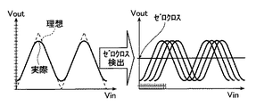
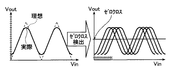
なお、図7に示すように、フォールディング信号は、図中点線で示す理想的な波形に対して、実際の波形は、その山部および谷部において特性の劣化が生じるため、下位ビットの変換精度が悪化する。 As shown in FIG. 7, the folding signal has a characteristic deterioration in the peak and valley portions of the actual waveform compared to the ideal waveform indicated by the dotted line in the figure. Gets worse.
これを改善するために、例えば下位ADC回路36が2ビットである場合、その出力電圧が、アナログ信号の入力電圧Vinに対して、下位ADC回路36の1ビットに相当するアナログ信号の電圧ずつシフトされた4個のフォールディング信号を生成し、4個のコンパレータの各々において、4個のフォールディング信号の各々の電圧レベルと中心レベルとを同時に比較(ゼロクロス検出)することによって下位ビットを得るという手法が用いられている。
In order to improve this, for example, when the
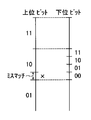
フォールディング型ADC30では、上位ADC回路32による上位ビットの変換結果とフォールディング回路34および下位ADC回路36による下位ビットの変換結果を加算(合成)することによって全体としての変換結果が得られる。しかし、上記の通り、上位ADC回路32による上位ビットの変換とフォールディング回路34および下位ADC回路36による変換は独立に行われるため、両者の間のミスマッチが起こる場合があるという問題がある。
In the
例えば、図8に示すように、アナログ信号の入力電圧が‘×’である場合、上位ビットの変換結果は‘01’、下位ビットの変換結果は‘00’となり、全体としての変換結果は‘0100’となる。しかし、下位ビットの変換結果を基準として考えれば、全体の変換結果は‘1000’となるべきである。このような上位ビットの変換結果と下位ビットの変換結果の間のミスマッチは、フォールディング回路34やコンパレータを構成するデバイスのばらつきによって生じる。
For example, as shown in FIG. 8, when the input voltage of the analog signal is “×”, the conversion result of the upper bits is “01”, the conversion result of the lower bits is “00”, and the conversion result as a whole is “ 0100 ′. However, if the conversion result of the lower bits is considered as a reference, the entire conversion result should be '1000'. Such a mismatch between the conversion result of the upper bits and the conversion result of the lower bits is caused by variations in the devices constituting the
この問題を解決する1つの手段として、エラー補正回路が知られている。図9は、上位2ビット、下位2ビットの2ステップフラッシュ型ADCで用いられるエラー補正回路の動作を説明する概念図である。エラー補正回路を用いることによって、例えば上位ビットの変換結果として‘10’が得られた場合、下位ADC回路では、上位ビットの変換結果である‘10’の範囲よりも広い範囲で下位ビットの変換が行われ、下位ビットの変換結果に応じて、上位ビットの変換結果が補正される。 An error correction circuit is known as one means for solving this problem. FIG. 9 is a conceptual diagram for explaining the operation of the error correction circuit used in the 2-step flash type ADC having the upper 2 bits and the lower 2 bits. For example, when “10” is obtained as the conversion result of the high-order bits by using the error correction circuit, the low-order ADC circuit converts the low-order bits in a wider range than the range of “10” that is the conversion result of the high-order bits. And the upper bit conversion result is corrected according to the lower bit conversion result.
ところで、上位2ビット、下位2ビットのADCの場合、必要なコンパレータ数は、理想的には上位3個、下位3個の合計6個である。これは、フラッシュ型で4ビットのADCを構成した場合の15個よりも少ないが、エラー補正を行うことによって、上記の例では上位3個、下位7個の合計10個のコンパレータ(図中○は下位ADC回路用のコンパレータ、●はエラー補正回路用のコンパレータである。)が必要となる。さらに、上位の変換結果を±1するための回路も必要となる。 By the way, in the case of the ADC of upper 2 bits and lower 2 bits, the number of necessary comparators is ideally 6 in total, that is, the upper 3 and the lower 3. This is less than 15 in the case of a flash type 4-bit ADC, but by performing error correction, in the above example, a total of 10 comparators (O Is a comparator for a low-order ADC circuit, and ● is a comparator for an error correction circuit). Further, a circuit for ± 1 of the upper conversion result is also required.
上記例は、フラッシュ型ADCのエラー補正回路であるが、フォールディング型ADCにおいても同様のエラー補正回路が必要となる。しかし、上記のように、従来のエラー補正回路では、その回路規模が大きくなりすぎるという問題があった。 The above example is an error correction circuit for a flash ADC, but a similar error correction circuit is also required for a folding ADC. However, as described above, the conventional error correction circuit has a problem that the circuit scale becomes too large.
本発明の目的は、前記従来技術に基づく問題点を解消し、フォールディング型ADCで用いられる回路規模の小さいエラー補正回路およびこのエラー補正回路を用いるフォールディング型ADCを提供することにある。 An object of the present invention is to solve the problems based on the prior art and provide an error correction circuit having a small circuit scale used in the folding ADC and a folding ADC using the error correction circuit.
上記目的を達成するために、本発明は、上位ビット変換用の上位A/Dコンバータ回路と、下位ビット変換用のフォールディング回路および下位A/Dコンバータ回路とを備えるフォールディング型のA/Dコンバータで用いられるエラー補正回路であって、
前記上位A/Dコンバータ回路への入力電圧範囲と前記下位A/Dコンバータ回路への入力電圧範囲とが、所定の電圧だけ高電位側または低電位側にシフトされており、
前記上位A/Dコンバータ回路から出力される上位ビットの変換結果のうちの最下位ビットと、前記下位A/Dコンバータ回路から出力され、前記フォールディング回路から出力される複数個のフォールディング信号のうちの1つのフォールディング信号について、その電圧レベルが、中心レベルよりも高電位の期間と低電位の期間とで異なる極性を持つ符号の極性に応じて、前記上位ビットの変換結果をそのまま出力する、もしくは前記上位ビットの変換結果から1を引くか1を加えるかのどちらかを行うことによって前記上位ビットの変換結果を補正することを特徴とするエラー補正回路を提供する。
To achieve the above object, the present invention is a folding type A / D converter comprising an upper A / D converter circuit for upper bit conversion, a folding circuit for lower bit conversion and a lower A / D converter circuit. An error correction circuit used,
An input voltage range to the upper A / D converter circuit and an input voltage range to the lower A / D converter circuit are shifted to a high potential side or a low potential side by a predetermined voltage,
The least significant bit of the conversion result of the upper bits output from the upper A / D converter circuit, and a plurality of folding signals output from the lower A / D converter circuit and output from the folding circuit For one folding signal, the conversion result of the upper bits is output as it is, depending on the polarity of the sign whose voltage level is different between the higher potential period and the lower potential period than the center level, or An error correction circuit is provided that corrects the conversion result of the upper bits by either subtracting 1 or adding 1 from the conversion result of the upper bits.
また、本発明は、上位ビット変換用の上位A/Dコンバータ回路と、下位ビット変換用のフォールディング回路および下位A/Dコンバータ回路と、エラー補正回路とを備えるフォールディング型のA/Dコンバータであって、
前記上位A/Dコンバータ回路は、アナログ信号の入力電圧に対応するデジタル信号の上位ビットを出力し、
前記フォールディング回路は、その出力電圧が、前記アナログ信号の入力電圧に対して、前記上位A/Dコンバータ回路の各々の基準電圧で順次折り返される出力特性を持ち、かつ前記下位A/Dコンバータ回路の1ビットに相当するアナログ信号の電圧ずつシフトされた複数個のフォールディング信号を出力し、
前記下位A/Dコンバータ回路は、前記フォールディング回路から出力される複数個のフォールディング信号に対応するデジタル信号の下位ビットを出力するとともに、前記フォールディング回路から出力される複数個のフォールディング信号のうちの1つのフォールディング信号の電圧レベルが、中心レベルよりも高電位の期間と低電位の期間とで異なる極性を持つ符号を出力し、
前記上位A/Dコンバータ回路への入力電圧範囲と前記下位A/Dコンバータ回路への入力電圧範囲とが、所定の電圧だけ高電位側または低電位側にシフトされており、
前記エラー補正回路は、前記上位A/Dコンバータ回路から出力される上位ビットの変換結果のうちの最下位ビットおよび前記下位A/Dコンバータ回路から出力されるフォールディング信号の符号の極性に応じて、前記上位ビットの変換結果をそのまま出力する、もしくは前記上位ビットの変換結果から1を引くか1を加えるかのどちらかを行うことによって前記上位ビットの変換結果を補正することを特徴とするA/Dコンバータを提供する。
Further, the present invention is a folding type A / D converter including an upper A / D converter circuit for upper bit conversion, a folding circuit and lower A / D converter circuit for lower bit conversion, and an error correction circuit. And
The upper A / D converter circuit outputs upper bits of a digital signal corresponding to an input voltage of an analog signal,
The folding circuit has an output characteristic in which an output voltage of the folding signal is sequentially folded at each reference voltage of the upper A / D converter circuit with respect to an input voltage of the analog signal, and the lower A / D converter circuit Outputs a plurality of folding signals shifted by the voltage of the analog signal corresponding to 1 bit,
The lower A / D converter circuit outputs lower bits of a digital signal corresponding to a plurality of folding signals output from the folding circuit and one of a plurality of folding signals output from the folding circuit. The voltage levels of the two folding signals are output with signs having different polarities in the high potential period and the low potential period than the center level,
An input voltage range to the upper A / D converter circuit and an input voltage range to the lower A / D converter circuit are shifted to a high potential side or a low potential side by a predetermined voltage,
The error correction circuit, according to the least significant bit of the conversion result of the upper bits output from the upper A / D converter circuit and the polarity of the sign of the folding signal output from the lower A / D converter circuit, The upper bit conversion result is corrected by either outputting the upper bit conversion result as it is or by subtracting 1 or adding 1 from the upper bit conversion result. A D converter is provided.
本発明によれば、上位A/Dコンバータ回路への入力電圧範囲と下位A/Dコンバータ回路への入力電圧範囲とが所定電圧だけシフトされており、あらかじめエラーが発生する状態に設定しておくことによって、エラー補正回路の簡素化を図ることができる。このため、エラー補正回路の回路規模、すなわちこのエラー補正回路を用いるフォールディング型A/Dコンバータの回路規模を大幅に削減することができる。 According to the present invention, the input voltage range to the higher-order A / D converter circuit and the input voltage range to the lower-order A / D converter circuit are shifted by a predetermined voltage, and the error voltage is set in advance. As a result, the error correction circuit can be simplified. For this reason, the circuit scale of the error correction circuit, that is, the circuit scale of the folding A / D converter using the error correction circuit can be greatly reduced.
以下に、添付の図面に示す好適実施形態に基づいて、本発明のエラー補正回路およびA/Dコンバータを詳細に説明する。 Hereinafter, an error correction circuit and an A / D converter of the present invention will be described in detail based on preferred embodiments shown in the accompanying drawings.
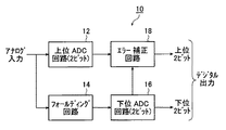
図1は、本発明のエラー補正回路を適用するA/Dコンバータの構成を表す一実施形態のブロック図である。同図に示すA/Dコンバータ(以下、ADCという)10は、アナログ信号の入力電圧に応じて、上位2ビット、下位2ビットの合計4ビットのデジタル信号を出力するフォールディング型のもので、上位ビット変換用の上位ADC回路12と、下位ビット変換用のフォールディング回路14および下位ADC回路16と、エラー補正回路18とを備えている。
FIG. 1 is a block diagram of an embodiment showing a configuration of an A / D converter to which an error correction circuit of the present invention is applied. The A / D converter (hereinafter referred to as ADC) 10 shown in the figure is a folding type that outputs a digital signal of a total of 4 bits, upper 2 bits and lower 2 bits, according to the input voltage of an analog signal. An
上位ADC回路12は、アナログ信号の入力電圧に対応するデジタル信号の上位2ビットD3,D2を出力する。
The
上位ADC回路12は、従来公知の構成のもので、例えば並列比較型ADC回路を用いることができる。この場合、上位ADC回路12では、図2に示すように、アナログ信号の入力電圧の最大値と最小値との間を4分割して得られる3レベルの基準電圧V1,V2,V3が用いられ、3個のコンパレータの各々において、アナログ信号の入力電圧と各々対応する基準電圧V1,V2,V3とを同時に比較することにより、アナログ信号の入力電圧に対応するデジタル信号の上位2ビットD3,D2を得る。
The
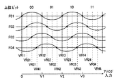
フォールディング回路14は、図2のタイミングチャートに示すように、下位ADC回路16における下位2ビットD1,D0のA/D変換に必要な電圧を有する4個のフォールディング信号F01,F02,F03,F04を生成する。
As shown in the timing chart of FIG. 2, the
フォールディング信号F01,F02,F03,F04の各々の出力電圧は、アナログ信号の入力電圧に対して、すなわち上位2ビットの変換結果‘00’、‘01’、‘10’、‘11’に対応して、上位ADC回路12の各々の基準電圧V1,V2,V3で順次折り返される出力特性を持つ。また、フォールディング信号F01,F02,F03,F04の各々は、その出力電圧が、アナログ信号の入力電圧に対して、下位ADC回路16の1ビットに相当するアナログ信号の電圧ずつシフトされている。
The output voltages of the folding signals F01, F02, F03, and F04 correspond to the input voltage of the analog signal, that is, the upper two bits of conversion results “00”, “01”, “10”, and “11”. Thus, the high-
下位ADC回路16は、フォールディング回路14から出力される4個のフォールディング信号F01,F02,F03,F04に対応するデジタル信号の下位2ビットD1,D0を出力する。
The
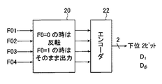
下位ADC回路16では、まず、例えば4個のコンパレータを用いて、各々対応するフォールディング信号F01,F02,F03,F04の電圧レベルと中心レベルとを同時に比較することにより、フォールディング信号F01,F02,F03,F04の各々の電圧レベルに対応する4ビットのデジタル値に変換する。デジタル値は、例えばフォールディング信号の電圧レベルが中心レベルよりも高電位側である場合を‘1’とし、低電位側である場合を‘0’とする。
In the
ここで、例えばフォールディング信号F01の電圧レベルが中心レベルよりも高電位側の期間を符号F0=‘1’とし、低電位側の期間を符号F0=‘0’とする。この符号F0=‘1’である場合、すなわちフォールディング信号の電圧レベルが中心レベルよりも高電位側である時は、図3に示すように、ビット反転回路20によりデジタル値をそのまま出力し、符号F0=‘0’である場合、すなわち低電位側である時はデジタル値を反転出力する。
Here, for example, a period in which the voltage level of the folding signal F01 is higher than the center level is denoted by a sign F0 = “1”, and a period in which the voltage level is lower is denoted by a sign F0 = “0”. When the sign F0 = '1', that is, when the voltage level of the folding signal is higher than the center level, the digital value is output as it is by the
そして、エンコーダ22により、ビット反転回路20から出力される4ビットのデジタル値をエンコードして、デジタル信号の下位2ビットD1,D0を得る。
Then, the
例えば、下記表1に示すように、フォールディング信号F01,F02,F03,F04のデジタル値=‘1000’である時、すなわちアナログ信号の入力電圧がVR11以上かつVR21未満の範囲である時、ビット反転回路20からは、デジタル値=‘1000’がそのまま出力され、これがエンコーダ22によってエンコードされて、デジタル信号の下位2ビットD1,D0=‘00’が出力される。デジタル値=‘1100’、‘1110’、‘1111’の場合も同様である。
For example, as shown in Table 1 below, when the digital values of the folding signals F01, F02, F03, and F04 = “1000”, that is, when the input voltage of the analog signal is in the range of VR11 or more and less than VR21, bit inversion is performed. From the
また、フォールディング信号F01,F02,F03,F04のデジタル値=‘0111’である時、すなわちアナログ信号の入力電圧がVR12以上かつVR22未満の範囲である時、ビット反転回路20からは、デジタル値=‘0111’の‘1’と‘0’が反転されて‘1000’が出力され、これがエンコーダ22によってエンコードされて、デジタル信号の下位2ビットD1,D0=‘00’が出力される。デジタル値=‘0011’、‘0001’、‘0000’の場合も同様である。
Further, when the digital values of the folding signals F01, F02, F03, and F04 = “0111”, that is, when the input voltage of the analog signal is in the range of VR12 or more and less than VR22, the digital value = The “1” and “0” of “0111” are inverted and “1000” is output, which is encoded by the
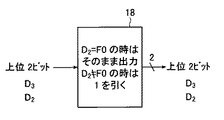
エラー補正回路18は、上位ADC回路12から出力される上位2ビットD3,D2の変換結果のうちの下位側のビットD2(上位ビットのうちの最下位ビット)および下位ADC回路16から出力されるフォールディング信号F01 ̄(フォールディング信号F01の反転信号)の符号F0に応じて、上位2ビットD3,D2の変換結果を補正する。
The
本実施形態の場合、図5に示すように、上位ADC回路12への入力電圧範囲は、下位ADC回路16への入力電圧範囲に対して、上位ADC回路12の1ビットに相当するアナログ信号の電圧範囲のおよそ半分の電圧だけ低電位側にシフトされている。この場合、エラー補正回路18からは、図4に示すように、上位ビットD2=符号F0であれば、上位2ビットD3,D2の変換結果がそのまま出力され、上位ビットD2≠符号F0の場合には、上位2ビットD3,D2の変換結果から‘1’を引いた値が出力される。
In the case of the present embodiment, as shown in FIG. 5, the input voltage range to the
図5に示すように、例えばアナログ信号の入力電圧が‘×’である場合、上位ADC回路12からは上位2ビットD3,D2=‘10’、下位ADC回路16からは下位2ビットD1,D0=‘10’が出力される。すなわち、上位ビットD2(=‘0’)≠フォールディング信号の符号F0(=‘1’)であるから、エラー補正回路18からは、上位2ビットD1,D0の変換結果である‘10’から1を引いて‘01’が上位2ビットの変換結果として出力され、全体の変換結果として‘0111’が得られる。
As shown in FIG. 5, for example, when the input voltage of the analog signal is “×”, the upper 2 bits D 3 and D 2 = “10” from the
また、アナログ信号の入力電圧が‘◎’である場合、上位ADC回路12からは上位2ビットD3,D2=‘01’、下位ADC回路16からは下位2ビットD1,D0=‘00’が出力される。すなわち、上位ビットD2(=‘1’)=フォールディング信号の符号F0(=‘1’)であるから、エラー補正回路18からは、上位2ビットD1,D0の変換結果である‘01’がそのまま上位2ビットの変換結果として出力され、全体の変換結果として‘0100’が得られる。
When the input voltage of the analog signal is “◎”, the upper 2 bits D 3 and D 2 = “01” from the
従来のフォールディング型ADCでは、上位ADC回路と下位ADC回路で使用する参照電圧を共通にすることによって可能な限りエラーの発生を少なくし、エラーが生じた場合に補正を行うようにしている。このため、エラー補正回路の回路規模が増大するという問題があった。これに対し、本発明のエラー補正回路18では、上記のように、あらかじめエラーが発生する状態に設定しておくことによって、エラー補正回路18の簡素化を図ることができる。このため、エラー補正回路18の回路規模、すなわちこのエラー補正回路18を用いるADC10の回路規模を大幅に削減することができる。
In the conventional folding ADC, the occurrence of errors is reduced as much as possible by using a common reference voltage for the upper ADC circuit and the lower ADC circuit, and correction is performed when an error occurs. For this reason, there is a problem that the circuit scale of the error correction circuit increases. On the other hand, in the
なお、デジタル信号の合計のビット数や、その上位ビットおよび下位ビットのビット数は何ら制限されない。 Note that the total number of bits of the digital signal and the number of upper bits and lower bits are not limited.
また、図5に示す例において、上位ADC回路12への入力電圧範囲を下位ADC回路16の入力電圧範囲に対して、上位ADC回路の1ビットに相当するアナログ信号の電圧範囲のおよそ半分の電圧だけ高電位側にシフトしてもよい。この場合、エラー補正回路18からは、上位ビットD2=符号F0であれば、上位2ビットD3,D2の変換結果がそのまま出力され、上位ビットD2≠符号F0の場合には、上位2ビットD3,D2の変換結果に‘1’を加えた値が出力される。
In the example shown in FIG. 5, the input voltage range to the higher-
また、上位ADC回路への入力電圧範囲と下位ADC回路への入力電圧範囲とを、どの程度シフトするかも適宜決定すればよいが、エラー補正回路において、簡単な回路でエラー検出を容易にするためには、上記のように、上位ADC回路への入力電圧範囲と下位ADC回路への入力電圧範囲とを、上位ADC回路の1ビットに相当するアナログ信号の電圧範囲のほぼ半分の電圧だけシフトするのが好ましい。 Further, it is only necessary to appropriately determine how much the input voltage range to the upper ADC circuit and the input voltage range to the lower ADC circuit are to be shifted. In order to facilitate error detection with a simple circuit in the error correction circuit. As described above, the input voltage range to the higher-order ADC circuit and the input voltage range to the lower-order ADC circuit are shifted by approximately half the voltage of the analog signal voltage range corresponding to one bit of the higher-order ADC circuit. Is preferred.
また、フォールディング信号の符号は、複数個あるフォールディング信号の中の任意の1つのフォールディング信号に基づいて決定すればよい。また、符号の極性も適宜変更してもよい。 The sign of the folding signal may be determined based on any one folding signal among the plurality of folding signals. Further, the polarity of the code may be changed as appropriate.
例えば、図5に示す例の場合、フォールディング信号F01の電圧レベルが中心レベルよりも高電位側の期間を符号F0=‘1’とし、低電位側の期間を符号F0=‘0’としているが、その逆に、フォールディング信号F01の電圧レベルが中心レベルよりも高電位側の期間を符号F0=‘0’とし、低電位側の期間を符号F0=‘1’としてもよい。 For example, in the case of the example shown in FIG. 5, the period when the voltage level of the folding signal F01 is higher than the center level is denoted by the sign F0 = '1', and the period when the voltage level is lower is denoted by the sign F0 = '0'. On the contrary, the period when the voltage level of the folding signal F01 is higher than the center level may be denoted by the sign F0 = “0”, and the period when the voltage level is lower than the center level may be denoted by the sign F0 = “1”.
すなわち、上位ビットの最下位ビットの極性、およびフォールディング信号の符号の極性に応じて、上位ビットの変換結果がそのまま出力される、もしくは上位ビットの変換結果から‘1’が引かれるか‘1’が加えられる。 That is, according to the polarity of the least significant bit of the upper bit and the polarity of the sign of the folding signal, the conversion result of the upper bit is output as it is, or is “1” subtracted from the conversion result of the upper bit? Is added.
本発明は、基本的に以上のようなものである。
以上、本発明のエラー補正回路およびA/Dコンバータについて詳細に説明したが、本発明は上記実施形態に限定されず、本発明の主旨を逸脱しない範囲において、種々の改良や変更をしてもよいのはもちろんである。
The present invention is basically as described above.
The error correction circuit and the A / D converter of the present invention have been described in detail above. However, the present invention is not limited to the above-described embodiment, and various improvements and modifications can be made without departing from the spirit of the present invention. Of course it is good.
10,30 A/Dコンバータ
12,32 上位ADC回路
14,34 フォールディング回路
16,36 下位ADC回路
18 エラー補正回路
20 ビット反転回路
22 エンコーダ
10, 30 A /
Claims (2)
前記上位A/Dコンバータ回路への入力電圧範囲と前記下位A/Dコンバータ回路への入力電圧範囲とが、所定の電圧だけ高電位側または低電位側にシフトされており、
前記上位A/Dコンバータ回路から出力される上位ビットの変換結果のうちの最下位ビットと、前記下位A/Dコンバータ回路から出力され、前記フォールディング回路から出力される複数個のフォールディング信号のうちの1つのフォールディング信号について、その電圧レベルが、中心レベルよりも高電位の期間と低電位の期間とで異なる極性を持つ符号の極性に応じて、前記上位ビットの変換結果をそのまま出力する、もしくは前記上位ビットの変換結果から1を引くか1を加えるかのどちらかを行うことによって前記上位ビットの変換結果を補正することを特徴とするエラー補正回路。 An error correction circuit used in a folding type A / D converter comprising an upper A / D converter circuit for upper bit conversion, a folding circuit for lower bit conversion and a lower A / D converter circuit,
An input voltage range to the upper A / D converter circuit and an input voltage range to the lower A / D converter circuit are shifted to a high potential side or a low potential side by a predetermined voltage,
The least significant bit of the conversion result of the upper bits output from the upper A / D converter circuit, and a plurality of folding signals output from the lower A / D converter circuit and output from the folding circuit For one folding signal, the conversion result of the upper bits is output as it is, depending on the polarity of the sign whose voltage level is different between the higher potential period and the lower potential period than the center level, or An error correction circuit, wherein the upper bit conversion result is corrected by either subtracting 1 or adding 1 from the upper bit conversion result.
前記上位A/Dコンバータ回路は、アナログ信号の入力電圧に対応するデジタル信号の上位ビットを出力し、
前記フォールディング回路は、その出力電圧が、前記アナログ信号の入力電圧に対して、前記上位A/Dコンバータ回路の各々の基準電圧で順次折り返される出力特性を持ち、かつ前記下位A/Dコンバータ回路の1ビットに相当するアナログ信号の電圧ずつシフトされた複数個のフォールディング信号を出力し、
前記下位A/Dコンバータ回路は、前記フォールディング回路から出力される複数個のフォールディング信号に対応するデジタル信号の下位ビットを出力するとともに、前記フォールディング回路から出力される複数個のフォールディング信号のうちの1つのフォールディング信号の電圧レベルが、中心レベルよりも高電位の期間と低電位の期間とで異なる極性を持つ符号を出力し、
前記上位A/Dコンバータ回路への入力電圧範囲と前記下位A/Dコンバータ回路への入力電圧範囲とが、所定の電圧だけ高電位側または低電位側にシフトされており、
前記エラー補正回路は、前記上位A/Dコンバータ回路から出力される上位ビットの変換結果のうちの最下位ビットおよび前記下位A/Dコンバータ回路から出力されるフォールディング信号の符号の極性に応じて、前記上位ビットの変換結果をそのまま出力する、もしくは前記上位ビットの変換結果から1を引くか1を加えるかのどちらかを行うことによって前記上位ビットの変換結果を補正することを特徴とするA/Dコンバータ。 A folding type A / D converter comprising an upper A / D converter circuit for upper bit conversion, a folding circuit and lower A / D converter circuit for lower bit conversion, and an error correction circuit,
The upper A / D converter circuit outputs upper bits of a digital signal corresponding to an input voltage of an analog signal,
The folding circuit has an output characteristic in which an output voltage of the folding signal is sequentially folded at each reference voltage of the upper A / D converter circuit with respect to an input voltage of the analog signal, and the lower A / D converter circuit Outputs a plurality of folding signals shifted by the voltage of the analog signal corresponding to 1 bit,
The lower A / D converter circuit outputs lower bits of a digital signal corresponding to a plurality of folding signals output from the folding circuit and one of a plurality of folding signals output from the folding circuit. The voltage levels of the two folding signals are output with signs having different polarities in the high potential period and the low potential period than the center level,
An input voltage range to the upper A / D converter circuit and an input voltage range to the lower A / D converter circuit are shifted to a high potential side or a low potential side by a predetermined voltage,
The error correction circuit, according to the least significant bit of the conversion result of the upper bits output from the upper A / D converter circuit and the polarity of the sign of the folding signal output from the lower A / D converter circuit, The upper bit conversion result is corrected by either outputting the upper bit conversion result as it is or by subtracting 1 or adding 1 from the upper bit conversion result. D converter.
Priority Applications (2)
| Application Number | Priority Date | Filing Date | Title |
|---|---|---|---|
| JP2004020922A JP3813614B2 (en) | 2004-01-29 | 2004-01-29 | Error correction circuit and A / D converter |
| US11/041,256 US6985097B2 (en) | 2004-01-29 | 2005-01-25 | Error correction circuit and A/D converter |
Applications Claiming Priority (1)
| Application Number | Priority Date | Filing Date | Title |
|---|---|---|---|
| JP2004020922A JP3813614B2 (en) | 2004-01-29 | 2004-01-29 | Error correction circuit and A / D converter |
Publications (2)
| Publication Number | Publication Date |
|---|---|
| JP2005217702A JP2005217702A (en) | 2005-08-11 |
| JP3813614B2 true JP3813614B2 (en) | 2006-08-23 |
Family
ID=34805595
Family Applications (1)
| Application Number | Title | Priority Date | Filing Date |
|---|---|---|---|
| JP2004020922A Expired - Lifetime JP3813614B2 (en) | 2004-01-29 | 2004-01-29 | Error correction circuit and A / D converter |
Country Status (2)
| Country | Link |
|---|---|
| US (1) | US6985097B2 (en) |
| JP (1) | JP3813614B2 (en) |
Families Citing this family (6)
| Publication number | Priority date | Publication date | Assignee | Title |
|---|---|---|---|---|
| US8155611B2 (en) * | 2007-12-31 | 2012-04-10 | Synopsys, Inc. | GPS baseband architecture |
| KR101584785B1 (en) * | 2009-01-21 | 2016-01-13 | 삼성전자주식회사 | - analog to digital converter and electronic system including the same |
| WO2011099367A1 (en) * | 2010-02-09 | 2011-08-18 | 日本電気株式会社 | A/d conversion device and a/d conversion correcting method |
| US8547257B2 (en) * | 2011-10-26 | 2013-10-01 | Texas Instruments Incorporated | Digital error correction in an analog-to-digital converter |
| KR102174204B1 (en) * | 2014-04-22 | 2020-11-05 | 에스케이하이닉스 주식회사 | Successive approximation register and single-slope analog-digital converting apparatus and method, and cmos image sensor thereof |
| US9941906B2 (en) | 2016-02-18 | 2018-04-10 | Samsung Electronics Co., Ltd. | Sliced polar codes |
Family Cites Families (3)
| Publication number | Priority date | Publication date | Assignee | Title |
|---|---|---|---|---|
| US5568149A (en) * | 1995-08-24 | 1996-10-22 | Motorola, Inc. | A/D converter subsystem with half linear buffer amplifier |
| JP3920443B2 (en) * | 1998-02-27 | 2007-05-30 | 株式会社ルネサステクノロジ | A / D conversion circuit |
| JP3520233B2 (en) * | 2000-01-21 | 2004-04-19 | 春夫 小林 | AD conversion circuit |
-
2004
- 2004-01-29 JP JP2004020922A patent/JP3813614B2/en not_active Expired - Lifetime
-
2005
- 2005-01-25 US US11/041,256 patent/US6985097B2/en active Active
Also Published As
| Publication number | Publication date |
|---|---|
| US20050168368A1 (en) | 2005-08-04 |
| US6985097B2 (en) | 2006-01-10 |
| JP2005217702A (en) | 2005-08-11 |
Similar Documents
| Publication | Publication Date | Title |
|---|---|---|
| TWI454064B (en) | Successive approximation analog-to-digital converter having auxiliary prediction circuit and method thereof | |
| JP5946443B2 (en) | Successive approximation register analog-to-digital converter with integral nonlinearity correction | |
| KR101007063B1 (en) | Method and apparatus correcting digital error of successive approximation analog to digital converter | |
| US8599059B1 (en) | Successive approximation register analog-digital converter and method for operating the same | |
| US8791845B2 (en) | Circuitry and method for reducing area and power of a pipelince ADC | |
| US8570206B1 (en) | Multi-bit per cycle successive approximation register ADC | |
| KR100690434B1 (en) | Digital to analog converter, data line driver, and display device and method thereof | |
| US9467161B1 (en) | Low-power, high-speed successive approximation register analog-to-digital converter and conversion method using the same | |
| JP4836574B2 (en) | Analog-to-digital converter and threshold correction method | |
| JP2007143140A (en) | Cascade-folding and interpolating type analog-to-digital converter | |
| US7675450B1 (en) | Digital-to-analog converter (DAC) for high frequency and high resolution environments | |
| JP4648779B2 (en) | Digital / analog converter | |
| JP3813614B2 (en) | Error correction circuit and A / D converter | |
| JP2006121378A (en) | A/d converter | |
| JP2012151728A (en) | Digital/analog converter | |
| JP5059796B2 (en) | Digital / analog converter | |
| KR20080042016A (en) | Analog-to-digital converter | |
| JP3782911B2 (en) | AD converter circuit | |
| US7999718B2 (en) | Analog-to-digital converter and electronic system including the same | |
| US10958284B2 (en) | Time-interleaved digital-to-analog converter with time-domain dynamic element matching and associated method | |
| US20090224951A1 (en) | Cyclic pipeline analog-to-digital converter | |
| KR102242402B1 (en) | Method of converting analog signal to digital information having a plurality of bits | |
| JP4513970B2 (en) | Multi-channel digital-analog converter | |
| US8018368B2 (en) | A/D converter | |
| JP5336638B2 (en) | Digital / analog converter |
Legal Events
| Date | Code | Title | Description |
|---|---|---|---|
| A977 | Report on retrieval |
Free format text: JAPANESE INTERMEDIATE CODE: A971007 Effective date: 20060501 |
|
| TRDD | Decision of grant or rejection written | ||
| A01 | Written decision to grant a patent or to grant a registration (utility model) |
Free format text: JAPANESE INTERMEDIATE CODE: A01 Effective date: 20060516 |
|
| A61 | First payment of annual fees (during grant procedure) |
Free format text: JAPANESE INTERMEDIATE CODE: A61 Effective date: 20060531 |
|
| R150 | Certificate of patent or registration of utility model |
Ref document number: 3813614 Country of ref document: JP Free format text: JAPANESE INTERMEDIATE CODE: R150 Free format text: JAPANESE INTERMEDIATE CODE: R150 |
|
| FPAY | Renewal fee payment (event date is renewal date of database) |
Free format text: PAYMENT UNTIL: 20090609 Year of fee payment: 3 |
|
| FPAY | Renewal fee payment (event date is renewal date of database) |
Free format text: PAYMENT UNTIL: 20100609 Year of fee payment: 4 |
|
| FPAY | Renewal fee payment (event date is renewal date of database) |
Free format text: PAYMENT UNTIL: 20110609 Year of fee payment: 5 |
|
| FPAY | Renewal fee payment (event date is renewal date of database) |
Free format text: PAYMENT UNTIL: 20110609 Year of fee payment: 5 |
|
| FPAY | Renewal fee payment (event date is renewal date of database) |
Free format text: PAYMENT UNTIL: 20120609 Year of fee payment: 6 |
|
| FPAY | Renewal fee payment (event date is renewal date of database) |
Free format text: PAYMENT UNTIL: 20120609 Year of fee payment: 6 |
|
| FPAY | Renewal fee payment (event date is renewal date of database) |
Free format text: PAYMENT UNTIL: 20130609 Year of fee payment: 7 |
|
| FPAY | Renewal fee payment (event date is renewal date of database) |
Free format text: PAYMENT UNTIL: 20130609 Year of fee payment: 7 |
|
| FPAY | Renewal fee payment (event date is renewal date of database) |
Free format text: PAYMENT UNTIL: 20140609 Year of fee payment: 8 |
|
| S111 | Request for change of ownership or part of ownership |
Free format text: JAPANESE INTERMEDIATE CODE: R313111 |
|
| R360 | Written notification for declining of transfer of rights |
Free format text: JAPANESE INTERMEDIATE CODE: R360 |
|
| R360 | Written notification for declining of transfer of rights |
Free format text: JAPANESE INTERMEDIATE CODE: R360 |
|
| R371 | Transfer withdrawn |
Free format text: JAPANESE INTERMEDIATE CODE: R371 |
|
| S111 | Request for change of ownership or part of ownership |
Free format text: JAPANESE INTERMEDIATE CODE: R313111 |
|
| R350 | Written notification of registration of transfer |
Free format text: JAPANESE INTERMEDIATE CODE: R350 |
|
| R250 | Receipt of annual fees |
Free format text: JAPANESE INTERMEDIATE CODE: R250 |
|
| R250 | Receipt of annual fees |
Free format text: JAPANESE INTERMEDIATE CODE: R250 |
|
| R250 | Receipt of annual fees |
Free format text: JAPANESE INTERMEDIATE CODE: R250 |
|
| R250 | Receipt of annual fees |
Free format text: JAPANESE INTERMEDIATE CODE: R250 |
|
| R250 | Receipt of annual fees |
Free format text: JAPANESE INTERMEDIATE CODE: R250 |
|
| R250 | Receipt of annual fees |
Free format text: JAPANESE INTERMEDIATE CODE: R250 |
|
| R250 | Receipt of annual fees |
Free format text: JAPANESE INTERMEDIATE CODE: R250 |
|
| R250 | Receipt of annual fees |
Free format text: JAPANESE INTERMEDIATE CODE: R250 |
|
| R250 | Receipt of annual fees |
Free format text: JAPANESE INTERMEDIATE CODE: R250 |
|
| R250 | Receipt of annual fees |
Free format text: JAPANESE INTERMEDIATE CODE: R250 |