JP3801410B2 - Semiconductor laser device and manufacturing method thereof - Google Patents
Semiconductor laser device and manufacturing method thereof Download PDFInfo
- Publication number
- JP3801410B2 JP3801410B2 JP2000059876A JP2000059876A JP3801410B2 JP 3801410 B2 JP3801410 B2 JP 3801410B2 JP 2000059876 A JP2000059876 A JP 2000059876A JP 2000059876 A JP2000059876 A JP 2000059876A JP 3801410 B2 JP3801410 B2 JP 3801410B2
- Authority
- JP
- Japan
- Prior art keywords
- layer
- dopant
- semiconductor laser
- cladding layer
- laser device
- Prior art date
- Legal status (The legal status is an assumption and is not a legal conclusion. Google has not performed a legal analysis and makes no representation as to the accuracy of the status listed.)
- Expired - Fee Related
Links
Images


Description
【0001】
【発明の属する技術分野】
本発明は、半導体レーザ素子に関し、特に活性領域における不純物分布を制御した半導体レーザ素子の構造及びその製造方法に関する。
【0002】
【従来の技術】
光ディスク用高出力レーザの光出射端面の劣化を抑制して、高出力で高信頼性を達成するために、端面及びその付近にレーザ光の吸収のない窓構造を設けた端面窓型レーザの開発が盛んに行われている。従来の端面窓型レーザの素子構造は、IEEE J.Quantum Electron.,vol.29,pp.1874−1879,1993に開示されている。
【0003】
図16に従来の素子構造の斜視図を示す。また、図17は図16のG−G’における断面図であり、図18は従来の半導体レーザ素子のリッジストライプ7内部のp型(以下、p−と標記)上クラッド層6表面からn型(以下、n−と標記)クラッド層2へのp型不純物(Zn)の濃度分布を示す図である。
【0004】
図16において、n−GaAs基板1上にn−AlGaInP下クラッド層2、アンドープガイド層3、DQW(Double Quantum Well)活性層4、MQB(Multi Quantum Barrier)層5、p−AlGaInP上クラッド層6を成長する。その後、光出射端面及びその付近に相当する成長層表面に、ZnOストライプ膜を選択的に形成し、それ以外の表面にはSiN膜を形成する。N2雰囲気、600℃で3時間の熱アニールを行うと、ZnOからZnが結晶中に拡散し、活性層のバンドギャップが増大する。ZnO膜、SiN膜を除去し、ZnOストライプ方向に垂直方向にリッジストライプ7を形成し、そのリッジストライプをn−GaAs電流阻止層8で埋め込み成長を行う。
【0005】
同時に、Zn拡散によりバンドギャップが増大した領域のリッジ上部を覆うように電流阻止層8を形成する。その後、成長層表面にp−GaAsコンタクト層9を形成する。基板側と成長層側に電極10、11を形成し、Zn拡散によりバンドギャップが増大した活性層が出射端面になるように、劈開を行う。光出射端面及びその付近に活性層のバンドギャップが増大した窓領域21と共振器内部の活性領域22が形成される。ここで、n−ドーパントにはSiを用い、p−ドーパントにはZnを用いる。
【0006】
図17に示すように、共振器内部の活性領域22では、リッジストライプ上部に電流阻止層は形成されておらず、共振器内部では活性層に電流が注入されてレーザ発振が起こる。
【0007】
従来の半導体レーザ素子では、波長670nmで最大光出力150mWが得られ、窓効果により端面劣化が抑制される。さらに、50℃、CW50mWの高出力で1500hrを超える信頼性が報告されている。
【0008】
図18に従来の半導体レーザ素子のリッジストライプ7内部のp−上クラッド層6表面からn−クラッド層2へのp−不純物(Zn)の濃度分布を示す。
【0009】
図18(a)に窓領域の濃度分布を、図18(b)に活性領域の濃度分布を示す。窓領域では、ZnO中のZnが活性層だけでなく、n−クラッド層の途中まで大量に拡散している。このZnの活性層への拡散が、バンドギャップ増大を生じさせる。活性領域においても、窓形成時の熱アニールに伴い、p−クラッド層6のZnが活性層4中、さらにn−クラッド層2中にまで拡散している。
【0010】
【発明が解決しようとする課題】
しかしながら、従来の半導体レーザ素子においては以下に示すような問題点がある。
【0011】
従来例の半導体レーザ素子では、窓領域を形成するため熱アニールを行うと、活性領域のp−クラッド層中のZnが活性層に拡散する。そのZnは活性層中に欠陥を生じるので、動作電流が増大するという問題が生じる。さらに、活性領域のp−クラッド層中のZnがn型クラッド層まで拡散すると、pn接合がn型クラッド層中に形成されて、動作電圧が増大するという問題が生じる。
【0012】
本発明は、上記に鑑みてなされたもので、低温または短時間の熱アニールにより所望の窓領域を形成でき、動作電流と動作電圧の増大を防止して、高信頼性の端面窓型高出力レーザの素子構造及びその製造方法を提供することを目的とする。
【課題を解決するための手段】
上記課題を解決するため、本発明の半導体レーザ素子では、半導体基板上に、n型クラッド層、活性層、p型クラッド層、p型キャップ層を有し、各半導体層に垂直な共振器端面を有し、共振器端面の少なくとも一方の端面付近における活性層のバンドギャップが共振器内部の活性層のバンドギャップよりも大きい窓領域を有する半導体レーザ素子であり、窓領域のp型クラッド層には第1ドーパントと第1ドーパントより拡散定数の大きい第2ドーパントとが混在し、該窓領域以外の活性領域のp型クラッド層には第1ドーパントが第2ドーパントより高濃度に存在し、該第1ドーパントと第2ドーパントの組み合わせが、各々ベリリウムと亜鉛、ベリリウムとマグネシウム、または、亜鉛とマグネシウム、であり、該窓領域上部のリッジ上部に電流阻止層を有し、その長さが窓領域の長さよりも長い構成としている。
【0013】
【0014】
【0015】
また、本発明の半導体レーザ素子では、窓領域のp型クラッド層のキャップ層側付近には主として第2ドーパントが配設され、窓領域のp型クラッド層の活性層側付近には主として第1ドーパントが配設される構成としている。
【0016】
【0017】
また、本発明の半導体レーザ素子では、窓領域のp型クラッド層のキャップ層側付近における第2ドーパントの濃度が1×1018cm-3以上、1×1019cm-3以下である構成としている。
【0018】
また、本発明の半導体レーザ素子では、p型クラッド層の活性層側付近における第1ドーパントの濃度が5×1017cm-3以上、3×1018cm-3以下である構成としている。
【0019】
【0020】
【0021】
また、本発明の半導体レーザ素子では、半導体の構成材料が、インジウム、ガリウム、リンを少なくとも含む構成としている。
【0022】
また、本発明の半導体レーザ素子の製造方法では、半導体基板上に、n型クラッド層、活性層、第1ドーパントを有するp型クラッド層とp型キャップ層を成長する工程、その上に共振器端面付近に相当する部分にのみ、第1ドーパントよりも拡散定数の大きな第2ドーパントとなる拡散源を形成する工程、次に熱アニールによりp型クラッド層に第2ドーパントを拡散して、p型クラッド層中の第1ドーパントの活性層への拡散を促進させて、活性層のバンドギャップを共振器内部よりも増大させて窓領域を形成する工程、とを少なくとも含み、該第1ドーパントと第2ドーパントの組み合わせが、各々ベリリウムと亜鉛、ベリリウムとマグネシウム、または、亜鉛とマグネシウム、である構成としている。
【0023】
【0024】
【発明の実施の形態】
図1〜図15は本発明の一実施の形態に関する半導体レーザ素子の図である。
【0025】
[第1の実施の形態]
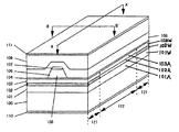
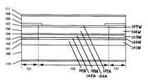
本発明の第1の実施の形態に関する端面窓型半導体レーザ素子の構造の斜視図を図1に、また、図1のA−A’断面図を図2に、図1のB−B’断面図を図3に、それぞれ示し、これを説明する。図から示されるように、図2はリッジストライプ中央部のリッジストライプの長手方向に平行な方向の断面図であり、図3は共振器中央部のリッジストライプの長手方向に垂直な方向の断面図である。
【0026】
図1において、n−GaAs基板100上に、n−(Al0.7Ga0.3)0.5In0.5P第1下クラッド層101(厚さ2μm、キャリヤ濃度1×1018cm-3、ドーパントSi)、ノンドープ多重量子井戸活性層102、p−(Al0.7Ga0.3)0.5In0.5P第1上クラッド層103(厚さ0.2μm、キャリヤ濃度1.5×1018cm-3、ドーパントBe)、p−In0.5Ga0.5Pエッチング停止層104(厚さ50Å、キャリヤ濃度1.5×1018cm-3、ドーパントBe)が形成されている。リッジストライプ105(幅5.0μm)は、p−(Al0.7Ga0.3)0.5In0.5Pよりなる第2上クラッド層106(厚さ1.2μm、キャリヤ濃度1.5×1018cm-3、ドーパントBe)と、p−GaAsキャップ層107(厚さ0.3μm、キャリヤ濃度1.5×1018cm-3、ドーパントBe))とから構成されている。
【0027】
ここに、ノンドープ多重量子井戸活性層102は、2層のIn0.5Ga0.5Pウエル層(厚さ80Å)とその間の1層の(Al0.5Ga0.5)0.5In0.5Pバリヤ層(厚さ50Å)とそれらを挟む(Al0.5Ga0.5)0.5In0.5Pガイド層(厚さ300Å)で構成されている。
【0028】
光出射端面及びその付近は、活性層のバンドギャップが共振器内部の活性層のバンドギャップよりも大きくなるように構成されている。
【0029】
リッジストライプ105の側面は、n−GaAs電流阻止層108(厚さ1.2μm、キャリヤ濃度1×1018cm-3、ドーパントSi)で埋め込まれており、光出射端面及びその付近ではリッジストライプの上部にn−GaAs電流阻止層108が形成されていてる。しかし、共振器内部のリッジストライプ上部には電流阻止層108が形成されていない。
【0030】
これらのリッジストライプ上部と電流阻止層の上部にはp−GaAsコンタクト層109(厚さ3μm、キャリヤ濃度2×1018cm-3、ドーパントBe)が形成されている。なお、本発明の半導体レーザ素子の共振器の長さは600μmである。また、基板側表面と成長層側表面には電極110、111が形成されている。
【0031】
また、本発明の第1の実施の形態に関する端面窓型半導体レーザ素子は、図1に示されるように、半導体の各層に対して垂直方向に、窓領域121と、活性領域122と、窓領域121とにわけることができる。
【0032】
従って、本発明の窓領域121に対しては、半導体の各層に窓領域を示すWを付与して、窓領域におけるn−第1下クラッド層101W、窓領域における量子井戸活性層102W、窓領域におけるp−第1上クラッド層103W、窓領域におけるリッジストライプ105W、窓領域におけるp−第2上クラッド層106W、窓領域におけるp−キャップ層107W、と呼ぶことにする。
【0033】
同様に、本発明の活性領域122に対しては、半導体の各層に活性領域を示すAを付与して、活性領域におけるn−第1下クラッド層101A、活性領域における量子井戸活性層102A、活性領域におけるp−第1上クラッド層103A、活性領域におけるリッジストライプ105A、活性領域におけるp−第2上クラッド層106A、活性領域におけるp−キャップ層107A、と呼ぶことにする。
【0034】
窓領域121は、端面窓型半導体レーザ素子の端面付近の領域のことであり、窓領域121の活性層(102W)のバンドギャップは、活性領域122の活性層(102A)のバンドギャップより大きく構成されている。
【0035】
従って、量子井戸活性層(活性層)102は、窓領域121の活性層(102W)と活性領域122の活性層(102A)と窓領域121の活性層(102W)とから構成される。
【0036】
また、活性層102に隣接する第1下クラッド層101は、窓領域121の第1下クラッド層(101W)と活性領域122の第1下クラッド層(101A)と窓領域121の第1下クラッド層(101W)とから構成される。
【0037】
同様に、活性層102に隣接する第1上クラッド層103は、窓領域121の第1上クラッド層(103W)と活性領域122の第1上クラッド層(103A)と窓領域121の第1上クラッド層(103W)とから構成される。
【0038】
ここに、活性領域122は主として、第1下クラッド層(101A)と活性層(102A)と第1上クラッド層(103A)と、及び、リッジストライプ105とから構成される言葉として用いられる。
【0039】
また、窓領域121は主として、第1下クラッド層(101W)と活性層(102W)と第1上クラッド層(103W)と、及び、リッジストライプ105とら構成される言葉として用いられる。図1〜図3では、この窓領域121は活性領域122の両側に配設されているが、少なくとも一方の端面にあれば、窓領域を有する半導体レーザ素子として機能する。
【0040】
図2に示すように、窓領域121の上部に窓領域を覆うように、窓領域よりも長く電流阻止層108が第2上クラッド層106の上に形成されている。
【0041】
図3に示すように、共振器内部の活性領域122では、リッジストライプ上部105(106及び107)に電流阻止層は形成されていない。
【0042】
また、図1〜図3において、窓領域のp−GaAsキャップ層107Wには、拡散定数の小さい第1ドーパントBeと拡散定数の大きい第2ドーパントZnとが混在し、Beの濃度は〜1.5×1018cm-3、Znの濃度は〜5×1018cm-3であり、(Znの濃度)>(Beの濃度)の関係にあり、(拡散定数の大きい第2ドーパントの濃度)>(拡散定数の小さい第1ドーパントの濃度)なる関係にある。
【0043】
また、図1〜図3において、窓領域以外の共振器内部のp−クラッド層106Aには、拡散定数の小さい第1ドーパント(例えば、Be)と拡散定数の大きい第2ドーパント(例えば、Zn)とが混在し、且つ、第1ドーパントの濃度が優位的に存在し、(Beの濃度)>(Znの濃度)の関係にあり、(拡散定数の小さい第1ドーパントの濃度)>(拡散定数の大きい第2ドーパントの濃度)なる関係にある。
【0044】
次に、用語として、「量子井戸活性層」や「活性層」や「量子井戸活性層の無秩序化」等について、説明する。
【0045】
本発明の端面窓型半導体レーザ素子においては、共振器端面付近の活性層のバンドギャップを共振器内部の活性層のバンドギャップよりも大きい構成としている。活性層が量子井戸活性層(各層の厚み0.02μm以下(200Å以下))の場合、活性層を変化させてバンドギャップを変化させることができるので、本発明では、主として、量子井戸活性層が用いられる。
【0046】
量子井戸活性層よりも厚みが厚いバルク活性層(厚み0.02μmより大)の場合、不純物等の拡散だけではバンドギャップは変化しない。しかし、活性層の組成を変化させるとバンドギャップは変化し、本発明の活性層として、バルク活性層を用いることも可能である。
【0047】
量子井戸活性層は、厚み0.02μm以下の量子井戸層と、量子井戸層と組成の異なるバリヤ層とを交互に積層する構造による得られる。この組成、または原子が秩序を有して配列している構造を秩序構造と呼ぶ。そして、不純物(例えば、p−ドーパントBe、Zn、Mg等)や空孔等の拡散や原子配列の変化等により、この秩序構造の破壊を「量子井戸活性層の無秩序化」と呼ぶ。量子井戸活性層の無秩序化により、活性層のバンドギャップは増大し、窓領域が形成される。バンドギャップ増大領域を共振器端面に配置することにより、端面劣化のない高信頼の高出力レーザが実現できる。
【0048】
また、バルク活性層においても組成が秩序を有して配列していたものを、組成を変化させてその秩序を崩すことを「活性層の無秩序化」と呼ぶことは可能である。
【0049】
次に、本発明の第1の実施の形態に関する端面窓型半導体レーザ素子の製造方法を図4に示し、これを説明する。図4(a)は、n−GaAs基板からp−キャップ層までの工程を示し、図4(b)は、ZnOXストライプの形成からSiO2キャップを形成するまでの工程を示し、図4(c)は、窓領域及び活性領域を形成工程を示し、図4(d)は、リッジストライプを形成する工程を示す図である。
【0050】
図4(a)において、n−GaAs基板100上に、分子線エピタキシー(MBE)法にて、n−(Al0.7Ga0.3)0.5In0.5P第1下クラッド層101(キャリヤ濃度1×1018cm-3、ドーパントSi)、(Al0.5Ga0.5)0.5In0.5Pガイド層と2層のIn0.5Ga0.5Pウエル層とその間の1層の(Al0.5Ga0.5)0.5In0.5Pバリヤ層と(Al0.5Ga0.5)0.5In0.5Pガイド層で構成されるノンドープ多重量子井戸活性層102、p−(Al0.7Ga0.3)0.5In0.5P第1上クラッド層103(キャリヤ濃度1.5×1018cm-3、ドーパントBe)、p−In0.5Ga0.5Pエッチング停止層104(キャリヤ濃度1.5×1018cm-3、ドーパントBe)、p−(Al0.7Ga0.3)0.5In0.5P第2上クラッド層106(キャリヤ濃度1.5×1018cm-3、ドーパントBe)とp−GaAsキャップ層107(厚さ0.3μm、キャリヤ濃度1.5×1018cm-3、ドーパントBe)を成長する。
【0051】
図4(b)において、ZnOX膜をp−キャップ層107表面に蒸着し、フォトリソグラフィとリフトオフにより、周期600μmで長さ50μmのZnOXストライプ131を形成し、その上にSiO2キャップ132を形成する。
【0052】
図4(c)において、500℃で3時間のアニールを行い、ZnOXストライプ列131直下の量子井戸活性層102に、第1上クラッド層103及び第2上クラッド層106のドーパントBeを拡散して、活性層のバンドギャップ増大領域、即ち窓領域121を形成する。同時にZnOストライプ列のない部分には活性領域122が形成される。
【0053】
ドーパントBe(第1ドーパント)を活性層に拡散することにより、活性層のバンドギャップは増大する。ドーパントZn(第1ドーパントより拡散定数の大きい第2ドーパント)はドーパントBe(第1ドーパント)の活性層への拡散を促進する働きをなしていると考えられる。
【0054】
この工程により、活性層102は、窓領域121の活性層(102W)と活性領域122の活性層(102A)と窓領域121の活性層(102W)となる。同様に、活性層102に隣接する第1上クラッド層103は、窓領域121の第1上クラッド層(103W)と活性領域122の第1上クラッド層(103A)と窓領域121の第1上クラッド層(103W)となる。同様に、活性層102に隣接する第1下クラッド層101は、窓領域121の第1下クラッド層(101W)と活性領域122の第1下クラッド層(101A)と窓領域121の第1下クラッド層(101W)となる。
【0055】
図4(d)において、ZnOXストライプ131とSiO2キャップ132を除去し、フォトリソグラフィとエッチングにより、リッジストライプ105を形成する。
【0056】
リッジストライプの側面及び窓領域のリッジストライプ上部に、n−GaAs電流阻止層108を第2回目のMBE法で埋め込み成長を行い、それら上部にp−GaAsコンタクト層109(厚さ3μm)を第3回目のMBE法で成長を行い、基板側とコンタクト層表面に電極を形成する(ここでは、これらの製造方法の詳細は図示せず。)。
【0057】
窓領域が共振器端面になるように、リッジストライプに直交した面で劈開を行い、光出射側端面に反射率8%のコーティングと裏面側に95%のコーティングを行う。ここで、共振器長は600μm、窓領域の長さは25μmである。
【0058】
本発明の半導体レーザ素子のn−電極111とp−電極112に、電圧を印加して、活性領域122のリッジストライプ内部とそれに相当する活性層に電流を注入することにより、光出射端面からレーザ発振光が得られる。波長655nmで、最大光出力250mWが得られ、窓効果により端面劣化が抑制される。さらに、動作温度60℃、連続発振70mWの高出力で5000hを超える高信頼性が得られた。
【0059】
従来の半導体レーザ素子の発振閾値電流が53mAであるのに対して、本発明の半導体レーザ素子の発振閾値電流は45mAに低減できた。また、従来の半導体レーザ素子の光出力50mWの動作電圧が2.5Vに対して、本発明の半導体レーザ素子の動作電圧は2.3Vまで低減できた。電流低減と電圧低減により、本発明の半導体レーザ素子では従来の半導体レーザ素子以上の高出力で高信頼性が達成できた。
【0060】
図5に、本発明の第1の実施の形態に関する端面窓型半導体レーザ素子のp−キャップ層107表面からn−クラッド層101へのp−不純物(Zn、Be)の濃度分布を示す。図5において、縦軸はp−不純物(Zn、Be)の濃度、横軸は各層の領域を示す。図5(a)に窓領域121の各層の濃度分布を、図5(b)に活性領域122の各層の濃度分布を示す。
【0061】
図5(a)の窓領域において、Zn(第2ドーパント)は、p−GaAsキャップ層107W表面(5×1018cm-3)からp−クラッド層106W中へと拡散分布し、〜1×1017cm-3以下となっている。
【0062】
また、Be(第1ドーパント)は、p−GaAsキャップ層107W表面(1.5×1018cm-3)から、第2上クラッド層106W、第1上クラッド層103W、ノンドープ多重量子井戸活性層102W、第1下クラッド層101Wへと及び、各層において、Be濃度は1.5×1018cm-3程度でほぼ一定の濃度分布となっている。このBe拡散により、窓領域121の活性層102Wのバンドギャップ増大せさている。
【0063】
図5(b)の活性領域において、Znは、ほとんど拡散分布せず、一方、Beは、p−GaAsキャップ層107A表面(〜1.5×1018cm-3)から、第2上クラッド層106A、第1上クラッド層103A、まで拡散分布し、ノンドープ多重量子井戸活性層102A、第1下クラッド層101へは、ほとんど拡散していないこと(〜1×1017cm-3以下であること)が示されている。
【0064】
図5(a)、図5(b)の結果から、次のことが明察される。本発明の第1の実施の形態に関する端面窓型半導体レーザ素子の窓領域には、p−ドーパントのBe(第1ドーパント)とp−ドーパントのZn(第2ドーパント)とが混在している。一方、活性領域では、p−ドーパントのBe(第1ドーパント)がp−ドーパントのZn(第2ドーパント)より高濃度に存在する。また、窓領域のp−クラッド層の活性層側付近には主として第1ドーパントが存在する。
【0065】
図5(a)、図5(b)の結果から、次のことが明察される。本発明の第1の実施の形態に関する端面窓型半導体レーザ素子の活性領域のp−クラッド層には、第1ドーパントの濃度が優位的に存在する。また、活性領域の活性層またはn−クラッド層に、第1ドーパントがほとんど存在しない。
【0066】
Znの拡散定数は、例えば、GaAs中において、700℃では、4×10-14cm-2/s程度であり、Beの拡散定数は、例えば、GaAs中において、725℃では、4×10-16cm-2/s程度であり、Znの拡散定数は、Beの拡散定数より2桁程度大きい。また、この拡散定数の大小関係は、インジウム、ガリウム、リンを少なくとも含む半導体材料においても同じであると考えられる(特開平8−102567号公報参照)言い換えれば、本発明のAl−In−Ga−P系の半導体層107、106、103、102、101、の各層においても、第2ドーパントZnの拡散定数は、第1ドーパントBeの拡散定数よりも大きい。また、この系において、Mg、Zn、Beの拡散定数の大小関係は、Mg>Zn>Beであると推察される。
【0067】
従来の半導体レーザ素子が600℃3時間のアニールであったのに対し、本発明の第1の実施の形態に関する端面窓型半導体レーザ素子の窓領域形成は、500℃3時間のアニールと、低温アニールで形成することができた。こはれ、キャップ層表面から拡散定数の大きなZnがp−クラッド層中に拡散し、それがp−クラッド層中のドーパントBeの活性層への拡散を促進するように作用したためと推察される。このBeの活性層への拡散に伴い、活性層のバンドギャップが増大し、窓領域が形成される。
【0068】
本発明の第1の実施の形態に関する端面窓型半導体レーザ素子では、従来の半導体レーザ素子よりも低温アニールで窓領域を形成できるので、活性領域において、p−クラッド層中のドーパント(Be)の活性層への拡散を抑制でき、動作電流及び動作電圧の増大を防止でき、高信頼性の高出力レーザが得られる。
【0069】
さらに、活性領域のp−クラッド層のドーパントに拡散定数の小さなBeを配設することにより、窓領域形成時の熱アニールで活性領域のBeが活性層に拡散することを防止でき、動作電流及び動作電圧増大に対して、さらに効果的である。本発明の第1の実施の形態に関する端面窓型半導体レーザ素子では、窓領域におけるp−ドーパントのZn濃度が、p−クラッド層のドーパントのBe濃度よりも高く設定されている。本構成により、Zn拡散がp−クラッド層中のBe拡散を促進する効果がさらに大きくなる。
【0070】
また、本発明の第1の実施の形態に関する端面窓型半導体レーザ素子の窓領域におけるキャップ層、または、p−クラッド層のキャップ層側付近のZn濃度が、1×1018cm-3以上、1×1019cm-3以下である。Zn濃度が1×1018cm-3よりも小さいと、p−クラッド層のBe拡散を促進する効果が小さくなる。
【0071】
また、Zn濃度が1×1019cm-3よりも大きいと、p−キャップ層付近のp−クラッド層に大量のZnが拡散してキャリヤを生成する。そのために、レーザ光に対するp−クラッド層のフリーキャリヤ吸収が増大する。また、大量のZn拡散はp−クラッド層中に結晶欠陥を生じやすくなり、そのためにレーザ光の吸収が生じる。
【0072】
また、p−クラッド層中のBe濃度は素子抵抗を低減し、且つ、フリーキャリヤ吸収を低減するために、通常、1〜3×1018cm-3程度に設定される。従って、キャップ層側付近のZn濃度が、1×1018cm-3以上に設定すれば、Zn濃度はBe濃度と同等以上の濃度になるので、Znがp−クラッド層中に拡散しやすくなり、それが、p−クラッド層中のBeの活性層への拡散を促進し、窓領域の活性層のバンドギャップを増大させることができる。
【0073】
また、本発明の半導体レーザ素子のp−クラッド層の活性層付近におけるBe濃度は〜5×1017cm-3以上、3×1018cm-3以下である。Be濃度が〜5×1017cm-3よりも小さくなると、窓領域における活性層へのBeの拡散が少なくなり、窓領域の活性層のバンドギャップ増大効果が低減する。Be濃度が3×1018cm-3よりも大きくなると、活性領域における活性層へのBe拡散が増大して、動作電流及び動作電圧が増大する。
【0074】
窓領域の上部における電流阻止層の長さは窓領域を覆うように、窓領域よりも長くなるように設定されるのが望ましい。これは、窓領域ではp−キャップ層からp−クラッド層に第2ドーパントが拡散されて第1ドーパントとの混在領域が形成されている。電流阻止層の長さを窓領域の長さよりも長くすることにより、この混在領域に電流を流すことを抑制できる。この混在領域に電流を流すと素子動作中に拡散がさらに促進し、素子特性の変動を生じる。従って、安定動作のために電流阻止層の長さを最適化することが望ましい。
【0075】
また、本発明の実施の形態に関する端面窓型半導体レーザ素子の材料系はIn、Ga、Pを少なくとも含有する。この場合、窓領域形成時の熱アニールで、第2ドーパントの拡散が第1ドーパントの拡散増大に特に有効に作用し、所望の窓領域形成に対して好適である。
【0076】
[第2の実施の形態]
本発明の第2の実施の形態に関する端面窓型半導体レーザ素子の構造の斜視図を図6に、また、図6のC−C’断面図を図7に、図6のD−D’断面図を図8に、それぞれ示し、これを説明する。図から示されるように、図7はリッジストライプ中央部のリッジストライプの長手方向に平行な方向の断面図であり、図8は共振器中央部のリッジストライプの長手方向に垂直な方向の断面図である。
【0077】
第1の実施の形態に関する端面窓型半導体レーザ素子では、拡散定数の小さい第1ドーパントにBe、拡散定数の大きい第2ドーパントにZn選択したが、本発明の第2の実施の形態に関する端面窓型半導体レーザ素子では、拡散定数の小さい第1ドーパントにBe、拡散定数の大きい第2ドーパントにMgを選択した点が、主な相違点である。この相違点に着目して、説明する。
【0078】
図6において、n−GaAs基板200上に、n−(Al0.7Ga0.3)0.5In0.5P第1下クラッド層201(厚さ2μm、、キャリヤ濃度1.0×1018cm-3、ドーパントSi)、ノンドープ多重量子井戸活性層202、p−(Al0.7Ga0.3)0.5In0.5P第1上クラッド層203(厚さ0.2μm、キャリヤ濃度1.0×1018cm-3、ドーパントBe)、p−In0.5Ga0.5Pエッチング停止層204(厚さ50Å、キャリヤ濃度1.0×1018cm-3、ドーパントBe)がある。リッジストライプ205(幅2.5μm)はp−(Al0.7Ga0.3)0.5In0.5P第2上クラッド層206(厚さ1.2μm、キャリヤ濃度1.5×1018cm-3、ドーパントBe)とp−GaAsキャップ層207(厚さ0.3μm、キャリヤ濃度1.5×1018cm-3、ドーパントBe)で構成されている。
【0079】
ここに、ノンドープ多重量子井戸活性層202は、2層のIn0.5Ga0.5Pウエル層(厚さ80Å)とその間の1層の(Al0.5Ga0.5)0.5In0.5Pバリヤ層(厚さ50Å)とそれらを挟む(Al0.5Ga0.5)0.5In0.5Pガイド層(厚さ300Å)で構成されている。
【0080】
光出射端面及びその付近では、活性層のバンドギャップが共振器内部の活性層のバンドギャップよりも大きくなっている。リッジストライプ205の側面は、n−Al0.5In0.5P電流阻止層208(厚さ1.2μm、キャリヤ濃度1×1018cm-3、ドーパントSi)で埋め込まれており、光出射端面及びその付近ではリッジストライプの上部に電流阻止層208を有し、共振器内部のリッジストライプ上部には電流阻止層が形成されていない。これらのリッジストライプ上部と電流阻止層の上部には、p−GaAsコンタクト層209(厚さ3μm、キャリヤ濃度2×1018cm-3、ドーパントBe)が形成されている。なお、本発明の半導体レーザ素子の共振器の長さは600μmである。
【0081】
また、基板側表面と成長層側表面には電極210、211が形成されている。ここで、端面付近の活性層バンドギャップの大きな領域を窓領域221、共振器内部の活性層バンドキャップの小さな領域を活性領域222とする。
【0082】
本発明の第1の実施の形態に関する端面窓型半導体レーザ素子の窓領域121、共振器内部の活性層バンドキャップの小さな領域を活性領域122で述べたと同様に、活性層202、第1下クラッド層201、第1上クラッド層203等は、窓領域221及び活性領域222に対応して、符号が付与される。
【0083】
活性層202は、窓領域221の活性層(202W)と活性領域222の活性層(202A)と窓領域221の活性層(202W)とから構成される。
【0084】
また、活性層202に隣接する第1下クラッド層201は、窓領域221の第1下クラッド層(201W)と活性領域222の第1下クラッド層(201A)と窓領域221の第1下クラッド層(201W)とから構成される。
【0085】
活性層202に隣接する第1上クラッド層203は、窓領域221の第1上クラッド層(203W)と活性領域222の第1上クラッド層(203A)と窓領域221の第1上クラッド層(203W)とから構成される。
【0086】
図7に示すように、窓領域221の上部に窓領域を覆うように、電流阻止層208が形成されている。図8に示すように、共振器内部の活性領域では、リッジストライプ上部に電流阻止層は形成されていない。
【0087】
次に、本発明の第2の実施の形態に関する端面窓型半導体レーザ素子の製造方法を図9に示し、これを説明する。図9(a)は、n−GaAs基板からp−キャップ層までの工程を示し、図9(b)は、SiO2マスクを形成するまでの工程を示し、図9(c)は、窓領域及び活性領域を形成工程を示し、図9(d)は、リッジストライプを形成する工程を示す図である。
【0088】
図9(a)において、n−GaAs基板200上に、分子線エピタキシー(MBE)法にて、n−(Al0.7Ga0.3)0.5In0.5P第1下クラッド層201(キャリヤ濃度1×1018cm-3、ドーパントSi)、(Al0.5Ga0.5)0.5In0.5Pガイド層と2層のIn0.5Ga0.5Pウエル層とその間の1層の(Al0.5Ga0.5)0.5In0.5Pバリヤ層と(Al0.5Ga0.5)0.5In0.5Pガイド層で構成されるノンドープ多重量子井戸活性層202、p−(Al0.7Ga0.3)0.5In0.5P第1上クラッド層203(キャリヤ濃度1×1018cm-3、ドーパントBe)、p−In0.5Ga0.5Pエッチング停止層204(キャリヤ濃度1×1018cm-3、ドーパントBe)、p−(Al0.7Ga0.3)0.5In0.5P第2上クラッド層206(キャリヤ濃度1.5×1018cm-3、ドーパントBe)とp−GaAsキャップ層207(厚さ0.3μm、キャリヤ濃度1.5×1018cm-3、ドーパントBe)を成長する。
【0089】
図9(b)において、SiO2マスク231をp−キャップ層207表面に蒸着し、フォトリソグラフィとリフトオフにより、周期600μmで長さ560μmのSiO2マスク231を形成する。
【0090】
図9(c)において、次に、有機金属気相成長(MOCVD)法または液相成長(LPE)法にて、SiO2マスク以外に選択的に高濃度のp−GaAs拡散層232(厚さ2μm、キャリヤ濃度5×1018cm-3、ドーパントMgまたはZn)を成長する。
【0091】
図9(d)において、500℃で2.5時間のアニールを行い、GaAs拡散層232直下にMgを拡散し、その拡散によりp−クラッド層203、206のドーパントBeの量子井戸活性層202への拡散を促進して、活性層のバンドギャップ増大領域、即ち窓領域221を形成する。同時にGaAs拡散層232のない部分は活性領域222となる。最後に、GaAs拡散層、SiO2マスクを除去し、フォトリソグラフィとエッチングによりリッジストライプ205を形成する。
【0092】
リッジストライプの側面及び窓領域のリッジストライプ上部に、n−Al0.5In0.5P電流阻止層208を第2回目のMBE法で埋め込み成長を行い、それら上部にp−GaAsコンタクト層209(厚さ3μm)を第3回目のMBE法で成長を行い、基板側とコンタクト層表面に電極を形成する(ここでは、これらの製造方法の詳細は図示せず。)。
【0093】
窓領域が共振器端面になるように、リッジストライプに直交した面で劈開を行い、光出射側端面に反射率8%のコーティングと裏面側に95%のコーティングを行う。ここで、共振器長は600μm、窓領域の長さは20μmである。
【0094】
本発明の半導体レーザ素子の電極210と211に電圧を印加して、活性領域222のリッジストライプ内部とそれに相当する活性層に電流を注入することにより、光出射端面からレーザ発振光が得られる。波長650nmで最大光出力300mWが得られ、窓効果により端面劣化が抑制される。さらに、動作温度60℃、連続発振85mWの高出力で5000hを超える高信頼性が得られた。
【0095】
従来の半導体レーザ素子の発振閾値電流が53mAであるのに対して、本発明の半導体レーザ素子の発振閾値電流は35mAに低減できた。また、従来の半導体レーザ素子の光出力50mWの動作電圧が2.5Vに対して、本発明の半導体レーザ素子の動作電圧は2.2Vまで低減できた。電流低減と電圧低減により、本発明の半導体レーザ素子では従来の半導体レーザ素子以上の高出力で高信頼性が達成できた。
【0096】
図10に本発明の半導体レーザ素子のp−キャップ層207表面からn−クラッド層201へのp−不純物(Mg、Be)の濃度分布を示す。図10(a)に窓領域の濃度分布を、図10(b)に活性領域の濃度分布を示す。
【0097】
窓領域において、キャップ層表面からMgがp−クラッド層中に拡散している。一方、p−クラッド層のBeは活性層だけでなく、n−クラッド層の途中まで大量に拡散している。このBe拡散が、窓領域の活性層のバンドギャップを増大させる。これに対して、活性領域では、p−クラッド層のBeが活性領域の活性層にはほとんど拡散していない。
【0098】
本発明の第2の実施の形態に関する端面窓型半導体レーザ素子の窓領域にはp−ドーパントのMg(第2ドーパント)とp−クラッド層のドーパンのBe(第1ドーパント)が混在している。活性領域ではp−クラッド層のドーパントのBeが存在する。ここで、ドーパントの拡散定数はMgの方がBeよりも大きい。
【0099】
本発明の半導体レーザ素子で従来の半導体レーザ素子よりも低温かつ短時間のアニールで窓領域が形成されたのは、キャップ層表面から拡散定数の大きなMgがp−クラッド層中に拡散し、それがp−クラッド層中のドーパントBeの活性層への拡散を促進するように作用すると推定される。このBeの活性層への拡散に伴い、窓領域の活性層のバンドギャップが増大し、窓領域が形成される。
【0100】
本発明の第2の実施の形態に関する端面窓型半導体レーザ素子では、活性領域において、p−クラッド層中のドーパント(Be)の活性層への拡散を抑制でき、電流及び電圧の増大を防止でき、高信頼性の高出力レーザが得られる。
【0101】
さらに、活性領域のp−クラッド層のドーパントに拡散定数の小さなBeを配置することにより、窓領域形成時の熱アニールで活性領域のBeが活性層に拡散することをさらに防止でき、電流及び電圧増大に対して効果的である。
【0102】
本発明の第1及び第2の実施の形態に関する端面窓型半導体レーザ素子では、p−GaAs拡散層(ZnOXストライプ131、SiO2キャップ132等)のドーパントがMg、Znの場合に同様の効果が得られた。特にドーパントがMgの場合には、より低温かつ短時間のアニールで窓領域の形成が可能となった。これは、Mgの方がZnよりも、p−クラッド層中のBeの活性層への拡散促進効果が大きいためと推測される。
【0103】
[第3の実施の形態実施]
図11は本発明の第3の実施の形態に関する端面窓型半導体レーザの素子構造の斜視図である。また、図12は図11のE−E’に示すようにリッジストライプ中央でリッジストライプに平行方向の断面図、図13は図11のF−F’に示すように共振器中央部でのリッジストライプに垂直方向の断面図である。
【0104】
本発明の第1〜第3の実施の形態に関する端面窓型半導体レーザ素子の主な相違点は、第1の実施の形態では、拡散定数の小さい第1ドーパントにBe、拡散定数の大きい第2ドーパントにZnを選択した点であり、第2の実施の形態では、第1ドーパントにBe、第2ドーパントにMgを選択した点であり、第3の実施の形態では、第1ドーパントにZn、第2ドーパントにMgを選択した点である。図11において、n−GaAs基板300上に、n−(Al0.7Ga0.3)0.5In0.5P第1下クラッド層301(厚さ2μm、キャリヤ濃度1.0×1018cm-3、ドーパントSi)、2層のIn0.5Ga0.5Pウエル層(厚さ80Å)とその間の1層の(Al0.5Ga0.5)0.5In0.5Pバリヤ層(厚さ50Å)とそれらを挟む(Al0.5Ga0.5)0.5In0.5Pガイド層(厚さ300Å)で構成されるノンドープ多重量子井戸活性層302、p−(Al0.7Ga0.3)0.5In0.5P第1上クラッド層303(厚さ0.2μm、キャリヤ濃度1.5×1018cm-3、ドーパントZn)、p−In0.5Ga0.5Pエッチング停止層304(厚さ50Å、キャリヤ濃度1.5×1018cm-3、ドーパントZn)がある。リッジストライプ305(幅2.5μm)はp−(Al0.7Ga0.3)0.5In0.5P第2上クラッド層306(厚さ1.2μm、キャリヤ濃度1.5×1018cm-3、ドーパントZn)とp−GaAsキャップ層307(厚さ0.3μm、キャリヤ濃度1.5×1018cm-3、ドーパントMg)で構成されている。光出射端面及びその付近では、活性層のバンドギャップが共振器内部の活性層のバンドギャップよりも大きくなっている。リッジストライプ305の側面は、n−Al0.5In0.5P電流阻止層208(厚さ1.2μm、キャリヤ濃度1×1018cm-3、ドーパントSi)で埋め込まれており、光出射端面及びその付近ではリッジストライプの上部に電流阻止層308を有し、共振器内部のリッジストライプ上部には電流阻止層が形成されていない。これらのリッジストライプ上部と電流阻止層の上部にはp−GaAsコンタクト層309(厚さ3μm、キャリヤ濃度2×1018cm-3、ドーパントZn)が形成されている。なお、本発明の半導体レーザ素子の共振器の長さは600μmである。また、基板側表面と成長層側表面には電極310、311が形成されている。ここで、端面付近の活性層バンドギャップの大きな領域を窓領域321、共振器内部の活性層バンドキャップの小さな領域を活性領域322とする。
【0105】
図12に示すように、窓領域321の上部に窓領域を覆うように、電流阻止層308が形成されている。図13に示すように、共振器内部の活性領域では、リッジストライプ上部に電流阻止層は形成されていない。
【0106】
図14に、本発明の第3の実施の形態に関する端面窓型半導体レーザ素子の製造方法を示し、これを説明する。
【0107】
図14(a)において、本発明の半導体レーザ素子の製造方法について次に述べる。図14に素子製造方法を示す。n−GaAs基板300上に、有機金属気相成長(MOCVD)法にて、n−(Al0.7Ga0.3)0.5In0.5P第1下クラッド層301(キャリヤ濃度1×1018cm-3、ドーパントSi)、(Al0.5Ga0.5)0.5In0.5Pガイド層と2層のIn0.5Ga0.5Pウエル層とその間の1層の(Al0.5Ga0.5)0.5In0.5Pバリヤ層と(Al0.5Ga0.5)0.5In0.5Pガイド層で構成されるノンドープ多重量子井戸活性層302、p−(Al0.7Ga0.3)0.5In0.5P第1上クラッド層303(キャリヤ濃度1.5×1018cm−3、ドーパントZn)、p−In0.5Ga0.5Pエッチング停止層304(キャリヤ濃度1.5×1018cm-3、ドーパントZn)、p−(Al0.7Ga0.3)0.5In0.5P第2上クラッド層306(キャリヤ濃度1.5×1018cm-3、ドーパントZn)と高濃度p−GaAsキャップ層307(厚さ3μm、キャリヤ濃度6×1018cm-3、ドーパントMg)を成長する。
【0108】
図14(b)において、SiO2マスク331をp−キャップ層307表面に蒸着し、フォトリソグラフィとリフトオフにより、周期600μmで長さ60μmのSiO2マスク331を形成し、エッチングによりマスク以外の部分のp−キャップ層厚を0.2μmまで薄くする。
【0109】
図14(c)において、600℃で2時間のアニールを行い、p−キャップ層の厚い部分のMgを拡散し、その拡散によりp−クラッド層303、306のドーパントZnの量子井戸活性層202への拡散を促進して、活性層のバンドギャップ増大領域、即ち窓領域321を形成する。同時にp−キャップ層の薄い部分はMgの拡散が少なく、そのためにp−クラッド層のZnの活性層への拡散も少なくなり、活性層のバンドギャップはほとんど変化しない活性領域322となる。
【0110】
図14(d)において、SiO2マスク331を除去し、p−キャップ層307厚を調整して、フォトリソグラフィとエッチングによりリッジストライプ305を形成する。
【0111】
リッジストライプの側面及び窓領域のリッジストライプ上部に、n−Al0.5In0.5P電流阻止層308を第2回目のMOCVD法で埋め込み成長を行い、それら上部にp−GaAsコンタクト層309(厚さ3μm)を第3回目のMOCVD法で成長を行い、基板側とコンタクト層表面に電極を形成する。(ここでは、これらの製造方法の詳細は図示せず。)窓領域が共振器端面になるように、リッジストライプに直交した面で劈開を行い、光出射側端面に反射率8%のコーティングと裏面側に95%のコーティングを行う。ここで、共振器長は600μm、窓領域の長さは20μmである。
【0112】
本発明の第3の実施の形態に関する端面窓型半導体レーザ素子の電極310と311に電圧を印加して、活性領域のリッジストライプ内部とそれに相当する活性層に電流を注入することにより、光出射端面からレーザ発振光が得られる。波長650nmで最大光出力300mWが得られ、窓効果により端面劣化が抑制されている。さらに、動作温度60℃、連続発振75mWの高出力で、5000hを超える高信頼性が得られた。
【0113】
従来の半導体レーザ素子の発振閾値電流が53mAであったのに対して、本発明の第3の実施の形態に関する端面窓型半導体レーザ素子の発振閾値電流は約40mAであり、発振閾値電流を約13mA低減することができた。また、従来の半導体レーザ素子の光出力50mWの動作電圧が2.5Vに対して、本発明の端面窓型半導体レーザ素子の動作電圧は2.3Vであり、2.3Vまで低減することができた。電流低減と電圧低減により、本発明の端面窓型半導体レーザ素子では、従来の半導体レーザ素子以上の高出力と高信頼性とを達成することができた。図15に、本発明の第3の実施の形態に関する端面窓型半導体レーザ素子のp−キャップ層307表面からn−クラッド層301へのp−不純物(Mg、Zn)の濃度分布を示す。図15(a)に窓領域の濃度分布を、図15(b)に活性領域の濃度分布を示す。窓領域において、キャップ層表面からMgがp−クラッド層中に拡散している。p−クラッド層のZnが活性層だけでなく、n−クラッド層の途中まで大量に拡散している。このZn拡散が、バンドギャップ増大を生じさせる。これに対して、活性領域では、p−キャップ層のMgの拡散はすくなく、p−クラッド層のZnが活性層にはほとんど拡散していない。
【0114】
本実施の形態では1回目の結晶成長により形成したp−キャップ層の厚みを変化させることにより、窓領域と活性領域を形成でき、製造上簡易であるという特徴がある。
【0115】
以上、本実施の形態では、InGaAlP系材料について述べたが、それ以外にAlGaAs系材料の場合にも同様の効果が得られる。
【0116】
【発明の効果】
以上のように、本発明の半導体レーザ素子によれば、半導体基板上に、n型クラッド層、活性層、p型クラッド層、p型キャップ層を有し、各半導体層に垂直な共振器端面を有し、共振器端面の少なくとも一方の端面付近における活性層のバンドギャップが共振器内部の活性層のバンドギャップよりも大きい窓領域を有する半導体レーザ素子であり、窓領域のp型クラッド層には第1ドーパントと第1ドーパントより拡散定数の大きい第2ドーパントとが混在し、窓領域以外の活性領域のp型クラッド層には第1ドーパントが第2ドーパントより高濃度に存在する構成としている。
【0117】
従って、窓領域形成時に、拡散定数の大きいp型ドーパント(第2ドーパント)が拡散定数の小さいp型ドーパント(第1ドーパント)の拡散を促進して活性層を無秩序化するので、比較的低温または短時間のアニールで所望の窓領域を形成できる。その結果、活性領域でp型ドーパントが活性層に拡散することによる動作電流及び動作電圧の増大を防止でき、高出力で高信頼性の半導体レーザ素子を得ることができる。
【0118】
また、本発明の半導体レーザ素子によれば、窓領域のp型キャップ層における第2ドーパントの濃度が第1ドーパントの濃度より高く配設する構成としている。従って、窓領域形成時に、拡散定数の大きいp型ドーパント(第2ドーパント)が拡散定数の小さいp型ドーパント(第1ドーパント)の拡散を促進するので、比較的低温または短時間のアニールで所望の窓領域を形成できる。その結果、活性領域でp型ドーパントが活性層に拡散することによる動作電流及び動作電圧の増大を防止でき、高出力で高信頼性の半導体レーザ素子を得ることができる。
【0119】
また、本発明の半導体レーザ素子によれば、窓領域以外の共振器内部のp型クラッド層には第1ドーパントの濃度が優位的に存在する構成としている。
【0120】
従って、活性領域に拡散定数の小さなドーパント(第1ドーパント)を配設することにより、窓領域形成時の熱アニールで、p型第2ドーパントが活性領域の活性層に拡散することを防止できる。その結果、動作電流及び動作電圧の増大を防止でき、高出力で高信頼性の半導体レーザ素子を得ることができる。
【0121】
また、本発明の半導体レーザ素子によれば、窓領域のp型クラッド層のキャップ層側付近には主として第2ドーパントが配設され、窓領域のp型クラッド層の活性層側付近には主として第1ドーパントが配設される構成としている。
【0122】
従って、窓領域形成時の熱アニールで、拡散定数の大きな第2ドーパントが拡散定数の小さな第1ドーパントの活性層への拡散を効果的に促進する。従って、アニール温度のさらなる低温化を図ることができ、動作電流及び動作電圧の増大を防止できる。その結果、動作電流及び動作電圧の増大を防止でき、高出力で高信頼性の半導体レーザ素子を得ることができる。
【0123】
また、本発明の半導体レーザ素子によれば、活性領域の活性層またはn型クラッド層に、第1ドーパントがほとんど存在しない構成としている。
【0124】
従って、窓領域形成時の熱アニールで、活性領域での第1ドーパントの活性層またはn型クラッド層への拡散を抑制することにより、動作電流及び動作電圧の増大を防止でき、高出力で高信頼性の半導体レーザ素子を得ることができる。
【0125】
また、本発明の半導体レーザ素子によれば、窓領域のp型クラッド層のキャップ層側付近における第2ドーパントの濃度が1×1018cm-3以上、1×1019cm-3以下である構成としている。
【0126】
従って、第2ドーパントの濃度を所定の範囲に設定することにより、窓領域形成時の熱アニールに伴う特性悪化を防止することができる。
【0127】
また、本発明の半導体レーザ素子によれば、p型クラッド層の活性層側付近における第1ドーパントの濃度が5×1017cm-3以上、3×1018cm-3以下である構成としている。
【0128】
従って、第1ドーパントの濃度を所定の範囲に設定することにより、窓領域形成時の熱アニールに伴う特性悪化を防止することができる。
【0129】
また、本発明の半導体レーザ素子によれば、第1ドーパントと第2ドーパントの組み合わせが、各々ベリリウムと亜鉛、ベリリウムとマグネシウム、または、亜鉛とマグネシウム、である構成としている。
【0130】
従って、第1ドーパントと第2ドーパントの組合せを必要に応じて選択することができ、所望の窓領域を制御よく形成することができる。
【0131】
また、本発明の半導体レーザ素子によれば、窓領域上部のリッジ上部に電流阻止層を有し、その長さが窓領域の長さよりも長い構成としている。
【0132】
従って、窓領域のp型クラッド層への電流リークによる半導体レーザ素子の特性悪化を抑制でき、特性安定化に好適である。
【0133】
また、本発明の半導体レーザ素子によれば、半導体の構成材料が、インジウム、ガリウム、リンを少なくとも含む構成としている。
【0134】
従って、半導体の構成材料の選択の幅が大きくなり、所望の発振波長を持つ半導体レーザ素子を得ることができる。
【0135】
また、本発明の半導体レーザ素子の製造方法によれば、半導体基板上に、n型クラッド層、活性層、第1ドーパントを有するp型クラッド層とp型キャップ層を成長する工程、その上に共振器端面付近に相当する部分にのみ、第1ドーパントよりも拡散定数の大きな第2ドーパントとなる拡散源を形成する工程、次に熱アニールによりp型クラッド層に第2ドーパントを拡散して、p型クラッド層中の第1ドーパントの活性層への拡散を促進させて、活性層のバンドギャップを共振器内部よりも増大させて窓領域を形成する工程、とを少なくとも含み、該第1ドーパントと第2ドーパントの組み合わせが、各々ベリリウムと亜鉛、ベリリウムとマグネシウム、または、亜鉛とマグネシウム、である構成としている。
【0136】
従って、高出力で高信頼性の半導体レーザ素子を得るための制御性に優れた製造方法を得ることができる。
【0137】
【0138】
【図面の簡単な説明】
【図1】 本発明の第1の実施の形態に関する半導体レーザ素子の斜視図である。
【図2】 本発明の図1のA−A’断面図であり、リッジストライプ中央部のリッジストライプの長手方向に平行な方向の断面図である。
【図3】 本発明の図1のB−B’断面図であり、共振器中央部のリッジストライプの長手方向に垂直な方向の断面図である。
【図4】 本発明の第1の実施の形態に関する半導体レーザ素子の製造方法に関する図であり、(a)はn−GaAs基板からp−キャップ層までの工程を示す図、(b)はZnOXストライプの形成からSiO2キャップを形成するまでの工程を示す図、(c)は窓領域及び活性領域を形成工程を示す図、(d)はリッジストライプを形成する工程を示す図、である。
【図5】 本発明の第1の実施の形態に関する半導体レーザ素子のp−キャップ層107表面からn−クラッド層101へのp型不純物(Zn、Be)の濃度分布を示す図であり、(a)は窓領域121の各層の濃度分布を示す図であり、(b)は活性領域122の各層の濃度分布を示す図である。
【図6】 本発明の第2の実施の形態に関する半導体レーザ素子の斜視図である。
【図7】 本発明の図6のC−C’断面図であり、リッジストライプ中央部のリッジストライプの長手方向に平行な方向の断面図である。
【図8】 本発明の図6のD−D’断面図であり、共振器中央部のリッジストライプの長手方向に垂直な方向の断面図である。
【図9】 本発明の第2の実施の形態に関する半導体レーザ素子の製造方法に関する図であり、(a)はn−GaAs基板からp−キャップ層までの工程を示す図、(b)はZnOXストライプの形成からSiO2キャップを形成するまでの工程を示す図、(c)は窓領域及び活性領域を形成工程を示す図、(d)はリッジストライプを形成する工程を示す図、である。
【図10】 本発明の第2の実施の形態に関する半導体レーザ素子のp−キャップ層207表面からn−クラッド層201へのp型不純物(Mg、Be)の濃度分布を示す図であり、(a)は窓領域221の各層の濃度分布を示す図であり、(b)は活性領域222の各層の濃度分布を示す図である。
【図11】 本発明の第3の実施の形態に関する半導体レーザ素子の斜視図である。
【図12】 本発明の図6のC−C’断面図であり、リッジストライプ中央部のリッジストライプの長手方向に平行な方向の断面図である。
【図13】 本発明の図6のD−D’断面図であり、共振器中央部のリッジストライプの長手方向に垂直な方向の断面図である。
【図14】 本発明の第3の実施の形態に関する半導体レーザ素子の製造方法に関する図であり、(a)はn−GaAs基板からp−キャップ層までの工程を示す図、(b)はZnOXストライプの形成からSiO2キャップを形成するまでの工程を示す図、(c)は窓領域及び活性領域を形成工程を示す図、(d)はリッジストライプを形成する工程を示す図、である。
【図15】 本発明の第3の実施の形態に関する半導体レーザ素子のp−キャップ層307表面からn−クラッド層301へのp型不純物(Mg、Zn)の濃度分布を示す図であり、(a)は窓領域321の各層の濃度分布を示す図であり、(b)は活性領域322の各層の濃度分布を示す図である。
【図16】 従来例の半導体レーザ素子の斜視図である。
【図17】 従来例の図16のG−G’における断面図である。
【図18】 従来例の半導体レーザ素子のリッジストライプ7内部のp−上クラッド層6表面かn−クラッド層2へのp型不純物(Zn)の濃度分布を示す図であり、(a)は窓領域のZnの濃度分布を示す図であり、(b)は活性領域のZnの濃度分布を示す図である。
【符号の説明】
100、200、300 n−GaAs基板
101、201、301 n−第1下クラッド層
101A、201A、301A 活性領域におけるn−第1下クラッド層
101W、201W、301W 窓領域におけるn−第1下クラッド層
102、202、302 量子井戸活性層(活性層)
102A、202A、302A 活性領域における量子井戸活性層(活性層)
102W、202W、302W 窓領域における量子井戸活性層(活性層)
103、203、303 p−第1上クラッド層
103A、203A、303A 活性領域におけるp−第1上クラッド層
103W、203W、303W 窓領域におけるp−第1上クラッド層
104、204、304 p−エッチング停止層
105、205、305 リッジストライプ
105A、205A、305A 活性領域におけるリッジストライプ
105W、205W、305W 窓領域におけるリッジストライプ
106、206、306 p−第2上クラッド層
106A、206A、306A 活性領域におけるp−第2上クラッド層
106W、206W、306W 窓領域におけるp−第2上クラッド層
107、207、307 p−キャップ層
107A、207A、307A 活性領域におけるp−キャップ層
107W、207W、307W 窓領域におけるp−キャップ層
108、208、308 n−電流阻止層
109、209、309 p−コンタクト層
110、210、310 n−電極
111、211、311 p−電極
121、221、321 窓領域
122、222、322 活性領域
131 ZnOストライプ
132 SiO2キャップ
231、331 SiO2マスク
232 拡散層[0001]
BACKGROUND OF THE INVENTION
The present invention relates to a semiconductor laser device, and more particularly to a structure of a semiconductor laser device in which an impurity distribution in an active region is controlled and a manufacturing method thereof.
[0002]
[Prior art]
Development of an end-face window type laser with a window structure that does not absorb laser light at and near the end face to suppress deterioration of the light exit end face of the high-power laser for optical disks and achieve high reliability at high output. Has been actively conducted. The element structure of a conventional end window type laser is disclosed in IEEE J. Quantum Electron. , Vol. 29, pp. 1874-1879, 1993.
[0003]
FIG. 16 shows a perspective view of a conventional element structure. FIG. 17 is a cross-sectional view taken along the line GG ′ of FIG. 16, and FIG. 18 shows the n-type from the surface of the p-type (hereinafter referred to as p-)
[0004]
In FIG. 16, an n-AlGaInP
[0005]
At the same time, the current blocking layer 8 is formed so as to cover the top of the ridge in the region where the band gap is increased by Zn diffusion. Thereafter, a p-GaAs contact layer 9 is formed on the growth layer surface.
[0006]
As shown in FIG. 17, in the
[0007]
In the conventional semiconductor laser device, a maximum light output of 150 mW is obtained at a wavelength of 670 nm, and end face deterioration is suppressed by the window effect. Furthermore, reliability exceeding 1500 hr at a high output of 50 ° C. and CW of 50 mW has been reported.
[0008]
FIG. 18 shows the concentration distribution of p-impurity (Zn) from the surface of the p-
[0009]
FIG. 18A shows the concentration distribution of the window region, and FIG. 18B shows the concentration distribution of the active region. In the window region, Zn in ZnO diffuses in a large amount not only in the active layer but also in the middle of the n-cladding layer. This diffusion of Zn into the active layer causes an increase in the band gap. Also in the active region, Zn in the p-cladding
[0010]
[Problems to be solved by the invention]
However, the conventional semiconductor laser device has the following problems.
[0011]
In the conventional semiconductor laser device, when thermal annealing is performed to form the window region, Zn in the p-cladding layer in the active region diffuses into the active layer. Since the Zn causes defects in the active layer, there arises a problem that the operating current increases. Furthermore, when Zn in the p-cladding layer in the active region diffuses to the n-type cladding layer, a pn junction is formed in the n-type cladding layer, resulting in an increase in operating voltage.
[0012]
The present invention has been made in view of the above. A desired window region can be formed by thermal annealing at a low temperature or in a short time, and an increase in operating current and operating voltage is prevented, thereby providing a highly reliable end window type high output. It is an object of the present invention to provide a laser element structure and a manufacturing method thereof.
[Means for Solving the Problems]
In order to solve the above-described problems, in the semiconductor laser device of the present invention, a resonator end face having an n-type cladding layer, an active layer, a p-type cladding layer, and a p-type cap layer on a semiconductor substrate and perpendicular to each semiconductor layer. And a semiconductor laser device having a window region in which the band gap of the active layer in the vicinity of at least one end surface of the resonator is larger than the band gap of the active layer inside the resonator, and the p-type cladding layer in the window region Is a mixture of a first dopant and a second dopant having a larger diffusion constant than the first dopant, The The first dopant is present in a higher concentration than the second dopant in the p-type cladding layer in the active region other than the window region And the combination of the first dopant and the second dopant is beryllium and zinc, beryllium and magnesium, or zinc and magnesium, respectively, and has a current blocking layer on the ridge above the window region, and its length Is longer than the length of the window area It is configured.
[0013]
[0014]
[0015]
In the semiconductor laser device of the present invention, the second dopant is mainly disposed near the cap layer side of the p-type cladding layer in the window region, and the first dopant is mainly disposed near the active layer side of the p-type cladding layer in the window region. The dopant is arranged.
[0016]
[0017]
In the semiconductor laser device of the present invention, the concentration of the second dopant in the vicinity of the cap layer side of the p-type cladding layer in the window region is 1 × 10 18
[0018]
In the semiconductor laser device of the present invention, the concentration of the first dopant in the vicinity of the active layer side of the p-type cladding layer is 5 × 10 5. 17
[0019]
[0020]
[0021]
In the semiconductor laser device of the present invention, the semiconductor constituent material includes at least indium, gallium, and phosphorus.
[0022]
Also, in the method of manufacturing a semiconductor laser device of the present invention, a step of growing an n-type cladding layer, an active layer, a p-type cladding layer having a first dopant and a p-type cap layer on a semiconductor substrate, and a resonator thereon A step of forming a diffusion source serving as a second dopant having a diffusion constant larger than that of the first dopant only in a portion corresponding to the vicinity of the end face, and then, a second dopant is diffused into the p-type cladding layer by thermal annealing to form a p-type And promoting diffusion of the first dopant in the cladding layer into the active layer to increase the band gap of the active layer more than inside the resonator to form a window region. The combination of the first dopant and the second dopant is beryllium and zinc, beryllium and magnesium, or zinc and magnesium, respectively. It is configured.
[0023]
[0024]
DETAILED DESCRIPTION OF THE INVENTION
1 to 15 are diagrams of a semiconductor laser device according to an embodiment of the present invention.
[0025]
[First Embodiment]
FIG. 1 is a perspective view of the structure of an end window semiconductor laser device according to the first embodiment of the present invention, FIG. 2 is a sectional view taken along line AA ′ of FIG. 1, and FIG. This is illustrated in FIG. 3 and described. 2 is a cross-sectional view in a direction parallel to the longitudinal direction of the ridge stripe in the center of the ridge stripe, and FIG. 3 is a cross-sectional view in a direction perpendicular to the longitudinal direction of the ridge stripe in the center of the resonator. It is.
[0026]
In FIG. 1, n- (Al 0.7 Ga 0.3 ) 0.5 In 0.5 P first lower cladding layer 101 (
[0027]
Here, the non-doped multiple quantum well
[0028]
The light emitting end face and the vicinity thereof are configured such that the band gap of the active layer is larger than the band gap of the active layer inside the resonator.
[0029]
The side surface of the
[0030]
A p-GaAs contact layer 109 (
[0031]
In addition, as shown in FIG. 1, the edge window type semiconductor laser device according to the first embodiment of the present invention has a
[0032]
Therefore, for the
[0033]
Similarly, for the
[0034]
The
[0035]
Therefore, the quantum well active layer (active layer) 102 includes an active layer (102W) in the
[0036]
The first
[0037]
Similarly, the first
[0038]
Here, the
[0039]
Further, the
[0040]
As shown in FIG. 2, the
[0041]
As shown in FIG. 3, in the
[0042]
1 to 3, the p-
[0043]
1 to 3, in the p-
[0044]
Next, terms such as “quantum well active layer”, “active layer”, “disordering of quantum well active layer”, and the like will be described.
[0045]
In the end face window type semiconductor laser device of the present invention, the band gap of the active layer in the vicinity of the end face of the resonator is larger than the band gap of the active layer inside the resonator. When the active layer is a quantum well active layer (the thickness of each layer is 0.02 μm or less (200 μm or less)), the band gap can be changed by changing the active layer. Used.
[0046]
In the case of a bulk active layer (thickness greater than 0.02 μm) thicker than the quantum well active layer, the band gap does not change only by diffusion of impurities or the like. However, when the composition of the active layer is changed, the band gap changes, and a bulk active layer can be used as the active layer of the present invention.
[0047]
The quantum well active layer is obtained by a structure in which a quantum well layer having a thickness of 0.02 μm or less and a barrier layer having a composition different from that of the quantum well layer are alternately stacked. This composition or a structure in which atoms are arranged in order is called an ordered structure. The destruction of the ordered structure due to diffusion of impurities (for example, p-dopant Be, Zn, Mg, etc.) and vacancies, changes in atomic arrangement, etc. is called “disordering of the quantum well active layer”. Due to the disordering of the quantum well active layer, the band gap of the active layer increases and a window region is formed. By arranging the band gap increasing region on the end face of the resonator, a highly reliable high-power laser without end face deterioration can be realized.
[0048]
Also, in the bulk active layer, what is arranged in an ordered manner can be called “disordering of the active layer” to change the composition and destroy the order.
[0049]
Next, a manufacturing method of the end face window type semiconductor laser device according to the first embodiment of the present invention will be described with reference to FIG. FIG. 4A shows the process from the n-GaAs substrate to the p-cap layer, and FIG. 4B shows the ZnO. X From the formation of stripes to SiO 2 FIG. 4C shows a process for forming a window region and an active region, and FIG. 4D shows a process for forming a ridge stripe.
[0050]
In FIG. 4A, n- (Al is formed on an n-
[0051]
In FIG. 4B, ZnO X A film is deposited on the surface of the p-
[0052]
In FIG. 4C, annealing was performed at 500 ° C. for 3 hours to obtain ZnO. X The dopant Be of the first
[0053]
By diffusing the dopant Be (first dopant) into the active layer, the band gap of the active layer is increased. It is considered that the dopant Zn (second dopant having a larger diffusion constant than the first dopant) serves to promote diffusion of the dopant Be (first dopant) into the active layer.
[0054]
By this step, the
[0055]
In FIG. 4D, ZnO X Stripe 131 and SiO 2 The
[0056]
An n-GaAs
[0057]
Cleaving is performed on the surface orthogonal to the ridge stripe so that the window region becomes the end face of the resonator, and the light emitting side end face is coated with a reflectance of 8% and the back face is coated with 95%. Here, the resonator length is 600 μm, and the length of the window region is 25 μm.
[0058]
By applying a voltage to the n-
[0059]
Whereas the oscillation threshold current of the conventional semiconductor laser element is 53 mA, the oscillation threshold current of the semiconductor laser element of the present invention can be reduced to 45 mA. Further, the operating voltage of the semiconductor laser device of the present invention can be reduced to 2.3V, while the operating voltage of the conventional semiconductor laser device having an optical output of 50 mW is 2.5V. Due to the current reduction and voltage reduction, the semiconductor laser device of the present invention can achieve high reliability and higher output than the conventional semiconductor laser device.
[0060]
FIG. 5 shows the concentration distribution of p-impurities (Zn, Be) from the surface of the p-
[0061]
In the window region of FIG. 5A, Zn (second dopant) is formed on the surface of the p-
[0062]
Further, Be (first dopant) is formed on the surface of the p-
[0063]
In the active region of FIG. 5B, Zn hardly diffuses and distribution, while Be is the surface of the p-
[0064]
From the results shown in FIGS. 5A and 5B, the following can be clearly understood. In the window region of the end face window type semiconductor laser device according to the first embodiment of the present invention, p-dopant Be (first dopant) and p-dopant Zn (second dopant) are mixed. On the other hand, in the active region, the p-dopant Be (first dopant) is present at a higher concentration than the p-dopant Zn (second dopant). The first dopant is mainly present in the vicinity of the active region side of the p-cladding layer in the window region.
[0065]
From the results shown in FIGS. 5A and 5B, the following can be clearly understood. The concentration of the first dopant is predominantly present in the p-cladding layer in the active region of the edge window type semiconductor laser device according to the first embodiment of the present invention. Further, the first dopant is hardly present in the active layer or the n-cladding layer in the active region.
[0066]
For example, the diffusion constant of Zn is 4 × 10 4 at 700 ° C. in GaAs. -14 cm -2 The diffusion constant of Be is, for example, 4 × 10 4 at 725 ° C. in GaAs. -16 cm -2 The diffusion constant of Zn is about two orders of magnitude greater than the diffusion constant of Be. In addition, it is considered that the magnitude relationship of the diffusion constant is the same for a semiconductor material containing at least indium, gallium, and phosphorus (see JP-A-8-102567). In other words, the Al—In—Ga— of the present invention. Also in each of the P-based semiconductor layers 107, 106, 103, 102, 101, the diffusion constant of the second dopant Zn is larger than the diffusion constant of the first dopant Be. Further, in this system, the magnitude relationship of the diffusion constants of Mg, Zn, and Be is presumed to be Mg>Zn> Be.
[0067]
Whereas the conventional semiconductor laser device is annealed at 600 ° C. for 3 hours, the window region formation of the end face window type semiconductor laser device according to the first embodiment of the present invention is performed at a low temperature of 500 ° C. for 3 hours. It could be formed by annealing. This is presumably because Zn having a large diffusion constant diffused from the surface of the cap layer into the p-clad layer, which acted to promote diffusion of the dopant Be in the p-clad layer into the active layer. . As the Be diffuses into the active layer, the band gap of the active layer increases and a window region is formed.
[0068]
In the end face window type semiconductor laser device according to the first embodiment of the present invention, since the window region can be formed by low-temperature annealing as compared with the conventional semiconductor laser device, the dopant (Be) in the p-cladding layer is formed in the active region. Diffusion to the active layer can be suppressed, an increase in operating current and operating voltage can be prevented, and a highly reliable high-power laser can be obtained.
[0069]
Further, by arranging Be having a small diffusion constant in the dopant of the p-cladding layer in the active region, it is possible to prevent the Be in the active region from diffusing into the active layer due to thermal annealing at the time of forming the window region. This is more effective for increasing the operating voltage. In the end face window type semiconductor laser device according to the first embodiment of the present invention, the Zn concentration of the p-dopant in the window region is set higher than the Be concentration of the dopant in the p-cladding layer. With this configuration, the effect of Zn diffusion promoting Be diffusion in the p-cladding layer is further increased.
[0070]
The Zn concentration in the vicinity of the cap layer in the window region of the edge window type semiconductor laser device or the p-clad layer on the cap layer side according to the first embodiment of the present invention is 1 × 10. 18
[0071]
The Zn concentration is 1 × 10 19 cm -3 Is larger than that, a large amount of Zn diffuses in the p-cladding layer near the p-cap layer to generate carriers. Therefore, the free carrier absorption of the p-cladding layer with respect to the laser light increases. In addition, a large amount of Zn diffusion tends to cause crystal defects in the p-cladding layer, which causes absorption of laser light.
[0072]
In addition, the Be concentration in the p-cladding layer is usually 1 to 3 × 10 6 in order to reduce device resistance and reduce free carrier absorption. 18 cm -3 Set to degree. Accordingly, the Zn concentration near the cap layer side is 1 × 10 5. 18 cm -3 If the above is set, the Zn concentration becomes equal to or higher than the Be concentration, so that Zn easily diffuses into the p-cladding layer, which causes the diffusion of Be in the p-cladding layer into the active layer. And can increase the band gap of the active layer in the window region.
[0073]
Further, the Be concentration in the vicinity of the active layer of the p-cladding layer of the semiconductor laser device of the present invention is about 5 × 10 5. 17
[0074]
The length of the current blocking layer above the window region is preferably set to be longer than the window region so as to cover the window region. In the window region, the second dopant is diffused from the p-cap layer to the p-cladding layer to form a mixed region with the first dopant. By making the length of the current blocking layer longer than the length of the window region, it is possible to suppress a current from flowing through the mixed region. When a current is passed through the mixed region, diffusion is further promoted during the operation of the device, resulting in a change in device characteristics. Therefore, it is desirable to optimize the length of the current blocking layer for stable operation.
[0075]
Further, the material system of the end face window type semiconductor laser device according to the embodiment of the present invention contains at least In, Ga, and P. In this case, in the thermal annealing at the time of forming the window region, the diffusion of the second dopant particularly effectively acts on the increase in the diffusion of the first dopant, which is suitable for the desired window region formation.
[0076]
[Second Embodiment]
FIG. 6 is a perspective view of the structure of the end face window type semiconductor laser device according to the second embodiment of the present invention, FIG. 7 is a sectional view taken along the line CC ′ of FIG. 6, and FIG. This is illustrated in FIG. 8 and described. 7 is a cross-sectional view in the direction parallel to the longitudinal direction of the ridge stripe at the center of the ridge stripe, and FIG. 8 is a cross-sectional view in the direction perpendicular to the longitudinal direction of the ridge stripe at the center of the resonator. It is.
[0077]
In the edge window type semiconductor laser device according to the first embodiment, Be is selected as the first dopant having a small diffusion constant, and Zn is selected as the second dopant having a large diffusion constant. However, the edge window according to the second embodiment of the present invention The main difference in the type semiconductor laser device is that Be is selected as the first dopant having a small diffusion constant and Mg is selected as the second dopant having a large diffusion constant. Description will be made by paying attention to this difference.
[0078]
In FIG. 6, n- (Al 0.7 Ga 0.3 ) 0.5 In 0.5 P first lower cladding layer 201 (
[0079]
Here, the non-doped multiple quantum well
[0080]
At and near the light emitting end face, the band gap of the active layer is larger than the band gap of the active layer inside the resonator. The side surface of the
[0081]
[0082]
As described in the
[0083]
The
[0084]
The first
[0085]
The first
[0086]
As shown in FIG. 7, a
[0087]
Next, a method for manufacturing an end face window type semiconductor laser device according to the second embodiment of the present invention will be described with reference to FIG. FIG. 9A shows the process from the n-GaAs substrate to the p-cap layer, and FIG. 2 FIG. 9C shows a process for forming a window region and an active region, and FIG. 9D shows a process for forming a ridge stripe.
[0088]
In FIG. 9A, n- (Al is formed on an n-
[0089]
In FIG. 9B, SiO 2 A
[0090]
Next, in FIG. 9C,
[0091]
In FIG. 9D, annealing is performed at 500 ° C. for 2.5 hours, Mg is diffused immediately below the
[0092]
N-Al on the side of the ridge stripe and on the top of the ridge stripe in the window region 0.5 In 0.5 The P
[0093]
Cleaving is performed on the surface orthogonal to the ridge stripe so that the window region becomes the end face of the resonator, and the light emitting side end face is coated with a reflectance of 8% and the back face is coated with 95%. Here, the resonator length is 600 μm, and the length of the window region is 20 μm.
[0094]
By applying a voltage to the
[0095]
Whereas the oscillation threshold current of the conventional semiconductor laser element is 53 mA, the oscillation threshold current of the semiconductor laser element of the present invention can be reduced to 35 mA. Also, the operating voltage of the semiconductor laser device of the present invention can be reduced to 2.2V, while the operating voltage of the conventional semiconductor laser device with an optical output of 50 mW is 2.5V. Due to the current reduction and voltage reduction, the semiconductor laser device of the present invention can achieve high reliability and higher output than the conventional semiconductor laser device.
[0096]
FIG. 10 shows the concentration distribution of p-impurities (Mg, Be) from the surface of the p-
[0097]
In the window region, Mg diffuses from the cap layer surface into the p-cladding layer. On the other hand, Be in the p-cladding layer diffuses in a large amount not only in the active layer but also in the middle of the n-cladding layer. This Be diffusion increases the band gap of the active layer in the window region. On the other hand, in the active region, Be in the p-cladding layer hardly diffuses into the active layer in the active region.
[0098]
In the window region of the end face window type semiconductor laser device according to the second embodiment of the present invention, p-dopant Mg (second dopant) and p-cladding layer Dopan Be (first dopant) are mixed. . In the active region, the p-cladding layer dopant Be is present. Here, the diffusion constant of the dopant is larger in Mg than in Be.
[0099]
In the semiconductor laser device of the present invention, the window region was formed by annealing at a lower temperature and in a shorter time than the conventional semiconductor laser device. Mg having a large diffusion constant diffused from the cap layer surface into the p-cladding layer. Is presumed to act to promote diffusion of dopant Be in the p-cladding layer into the active layer. As the Be diffuses into the active layer, the band gap of the active layer in the window region increases, and a window region is formed.
[0100]
In the edge window type semiconductor laser device according to the second embodiment of the present invention, diffusion of the dopant (Be) in the p-cladding layer into the active layer can be suppressed in the active region, and an increase in current and voltage can be prevented. A highly reliable high-power laser can be obtained.
[0101]
Furthermore, by arranging Be having a small diffusion constant in the dopant of the p-cladding layer in the active region, it is possible to further prevent the Be in the active region from diffusing into the active layer by thermal annealing at the time of forming the window region. It is effective against increase.
[0102]
In the end face window type semiconductor laser device according to the first and second embodiments of the present invention, a p-GaAs diffusion layer (ZnO) is used. X
[0103]
[Third Embodiment]
FIG. 11 is a perspective view of an element structure of an end face window type semiconductor laser according to the third embodiment of the present invention. 12 is a cross-sectional view in the direction parallel to the ridge stripe at the center of the ridge stripe as indicated by EE ′ in FIG. 11, and FIG. 13 is a ridge at the center of the resonator as indicated by FF ′ in FIG. It is sectional drawing of a perpendicular direction to a stripe.
[0104]
The main difference between the end face window type semiconductor laser devices relating to the first to third embodiments of the present invention is that in the first embodiment, Be is a first dopant having a small diffusion constant, and a second is a large diffusion constant. In the second embodiment, Zn is selected as the dopant. In the second embodiment, Be is selected as the first dopant, and Mg is selected as the second dopant. In the third embodiment, the first dopant is Zn, This is that Mg is selected as the second dopant. In FIG. 11, n- (Al 0.7 Ga 0.3 ) 0.5 In 0.5 P first lower cladding layer 301 (
[0105]
As shown in FIG. 12, a
[0106]
FIG. 14 shows a manufacturing method of an end face window type semiconductor laser device according to the third embodiment of the present invention, which will be described.
[0107]
Next, referring to FIG. 14A, a method for manufacturing the semiconductor laser device of the present invention will be described. FIG. 14 shows an element manufacturing method. On the n-
[0108]
In FIG. 14B, SiO 2 A
[0109]
In FIG. 14C, annealing is performed at 600 ° C. for 2 hours to diffuse Mg in the thick part of the p-cap layer, and the diffusion causes the dopant Zn to the quantum well
[0110]
In FIG. 14 (d), SiO 2 The
[0111]
N-Al on the side of the ridge stripe and on the top of the ridge stripe in the window region 0.5 In 0.5 The P
[0112]
Light is emitted by applying a voltage to the
[0113]
Whereas the oscillation threshold current of the conventional semiconductor laser element is 53 mA, the oscillation threshold current of the end face window type semiconductor laser element according to the third embodiment of the present invention is about 40 mA, and the oscillation threshold current is about It was possible to reduce 13 mA. Further, the operating voltage of the conventional semiconductor laser device with an optical output of 50 mW is 2.5 V, whereas the operating voltage of the end face window type semiconductor laser device of the present invention is 2.3 V, which can be reduced to 2.3 V. It was. Due to the current reduction and voltage reduction, the end face window type semiconductor laser device of the present invention can achieve higher output and higher reliability than the conventional semiconductor laser device. FIG. 15 shows the concentration distribution of p-impurities (Mg, Zn) from the surface of the p-
[0114]
This embodiment is characterized in that the window region and the active region can be formed by changing the thickness of the p-cap layer formed by the first crystal growth, which is simple in manufacturing.
[0115]
As described above, the InGaAlP-based material has been described in the present embodiment, but the same effect can be obtained in the case of an AlGaAs-based material.
[0116]
【The invention's effect】
As described above, according to the semiconductor laser device of the present invention, the resonator end face has an n-type cladding layer, an active layer, a p-type cladding layer, and a p-type cap layer on the semiconductor substrate, and is perpendicular to each semiconductor layer. And a semiconductor laser element having a window region in which the band gap of the active layer in the vicinity of at least one end surface of the resonator is larger than the band gap of the active layer inside the resonator, and the p-type cladding layer in the window region Has a configuration in which a first dopant and a second dopant having a larger diffusion constant than the first dopant are mixed, and the first dopant is present in a higher concentration than the second dopant in the p-type cladding layer in the active region other than the window region. .
[0117]
Accordingly, when the window region is formed, the p-type dopant (second dopant) having a large diffusion constant promotes the diffusion of the p-type dopant (first dopant) having a small diffusion constant, thereby disordering the active layer. A desired window region can be formed by short-time annealing. As a result, an increase in operating current and operating voltage due to diffusion of the p-type dopant into the active layer in the active region can be prevented, and a semiconductor laser device with high output and high reliability can be obtained.
[0118]
In addition, according to the semiconductor laser device of the present invention, the second dopant concentration in the p-type cap layer in the window region is higher than the first dopant concentration. Therefore, when the window region is formed, the p-type dopant (second dopant) having a large diffusion constant promotes the diffusion of the p-type dopant (first dopant) having a small diffusion constant. A window region can be formed. As a result, an increase in operating current and operating voltage due to diffusion of the p-type dopant into the active layer in the active region can be prevented, and a semiconductor laser device with high output and high reliability can be obtained.
[0119]
In addition, according to the semiconductor laser device of the present invention, the concentration of the first dopant is preferentially present in the p-type cladding layer inside the resonator other than the window region.
[0120]
Therefore, by disposing a dopant having a small diffusion constant (first dopant) in the active region, it is possible to prevent the p-type second dopant from diffusing into the active layer in the active region by thermal annealing when forming the window region. As a result, an increase in operating current and operating voltage can be prevented, and a high output and high reliability semiconductor laser device can be obtained.
[0121]
According to the semiconductor laser device of the present invention, the second dopant is mainly disposed near the cap layer side of the p-type cladding layer in the window region, and mainly near the active layer side of the p-type cladding layer in the window region. The first dopant is arranged.
[0122]
Therefore, the second dopant having a large diffusion constant effectively promotes the diffusion of the first dopant having a small diffusion constant into the active layer in the thermal annealing at the time of forming the window region. Therefore, the annealing temperature can be further lowered, and an increase in operating current and operating voltage can be prevented. As a result, an increase in operating current and operating voltage can be prevented, and a high output and high reliability semiconductor laser device can be obtained.
[0123]
In addition, according to the semiconductor laser device of the present invention, the first dopant is hardly present in the active layer or the n-type cladding layer in the active region.
[0124]
Therefore, by suppressing the diffusion of the first dopant into the active layer or the n-type cladding layer in the active region by thermal annealing at the time of forming the window region, it is possible to prevent an increase in operating current and operating voltage, and a high output and high power. A reliable semiconductor laser element can be obtained.
[0125]
According to the semiconductor laser device of the present invention, the concentration of the second dopant in the vicinity of the cap layer side of the p-type cladding layer in the window region is 1 × 10 18
[0126]
Therefore, by setting the concentration of the second dopant within a predetermined range, it is possible to prevent the deterioration of characteristics due to the thermal annealing at the time of forming the window region.
[0127]
According to the semiconductor laser device of the present invention, the concentration of the first dopant in the vicinity of the active layer side of the p-type cladding layer is 5 × 10 5. 17
[0128]
Therefore, by setting the concentration of the first dopant within a predetermined range, it is possible to prevent the deterioration of characteristics due to the thermal annealing at the time of forming the window region.
[0129]
According to the semiconductor laser device of the present invention, the combination of the first dopant and the second dopant is beryllium and zinc, beryllium and magnesium, or zinc and magnesium, respectively.
[0130]
Therefore, a combination of the first dopant and the second dopant can be selected as necessary, and a desired window region can be formed with good control.
[0131]
According to the semiconductor laser device of the present invention, the current blocking layer is provided on the ridge above the window region, and the length thereof is longer than the length of the window region.
[0132]
Therefore, it is possible to suppress the deterioration of the characteristics of the semiconductor laser device due to the current leakage to the p-type cladding layer in the window region, which is suitable for stabilizing the characteristics.
[0133]
Further, according to the semiconductor laser device of the present invention, the semiconductor constituent material includes at least indium, gallium, and phosphorus.
[0134]
Therefore, the range of selection of semiconductor constituent materials is increased, and a semiconductor laser element having a desired oscillation wavelength can be obtained.
[0135]
According to the method for manufacturing a semiconductor laser device of the present invention, a step of growing an n-type cladding layer, an active layer, a p-type cladding layer having a first dopant and a p-type cap layer on a semiconductor substrate, A step of forming a diffusion source serving as a second dopant having a diffusion constant larger than that of the first dopant only in a portion corresponding to the vicinity of the end face of the resonator, and then diffusing the second dopant into the p-type cladding layer by thermal annealing, and promoting the diffusion of the first dopant in the p-type cladding layer into the active layer to increase the band gap of the active layer more than the inside of the resonator to form a window region. The combination of the first dopant and the second dopant is beryllium and zinc, beryllium and magnesium, or zinc and magnesium, respectively. It is configured.
[0136]
Therefore, it is possible to obtain a manufacturing method excellent in controllability for obtaining a semiconductor laser device having high output and high reliability.
[0137]
[0138]
[Brief description of the drawings]
FIG. 1 is a perspective view of a semiconductor laser device according to a first embodiment of the present invention.
FIG. 2 is a cross-sectional view taken along the line AA ′ of FIG. 1 of the present invention, and is a cross-sectional view in a direction parallel to the longitudinal direction of the ridge stripe at the center of the ridge stripe.
3 is a cross-sectional view taken along the line BB ′ of FIG. 1 according to the present invention, and is a cross-sectional view in a direction perpendicular to the longitudinal direction of the ridge stripe at the center of the resonator.
4A and 4B are diagrams relating to a method of manufacturing a semiconductor laser device according to the first embodiment of the present invention, in which FIG. 4A is a diagram illustrating a process from an n-GaAs substrate to a p-cap layer, and FIG. X From the formation of stripes to SiO 2 FIG. 4C is a diagram illustrating a process until a cap is formed, FIG. 4C is a diagram illustrating a process of forming a window region and an active region, and FIG. 4D is a diagram illustrating a process of forming a ridge stripe.
FIG. 5 is a diagram showing the concentration distribution of p-type impurities (Zn, Be) from the surface of the p-
FIG. 6 is a perspective view of a semiconductor laser device according to a second embodiment of the present invention.
7 is a cross-sectional view taken along the line CC ′ of FIG. 6 of the present invention, and is a cross-sectional view in a direction parallel to the longitudinal direction of the ridge stripe at the center of the ridge stripe.
8 is a cross-sectional view taken along the line DD ′ of FIG. 6 of the present invention, and is a cross-sectional view in a direction perpendicular to the longitudinal direction of the ridge stripe at the center of the resonator.
FIGS. 9A and 9B are diagrams relating to a method of manufacturing a semiconductor laser device according to a second embodiment of the present invention, wherein FIG. 9A is a diagram showing steps from an n-GaAs substrate to a p-cap layer, and FIG. X From the formation of stripes to SiO 2 FIG. 4C is a diagram illustrating a process until a cap is formed, FIG. 4C is a diagram illustrating a process of forming a window region and an active region, and FIG. 4D is a diagram illustrating a process of forming a ridge stripe.
FIG. 10 is a diagram showing the concentration distribution of p-type impurities (Mg, Be) from the surface of the p-
FIG. 11 is a perspective view of a semiconductor laser device according to a third embodiment of the present invention.
12 is a cross-sectional view taken along the line CC ′ of FIG. 6 of the present invention, and is a cross-sectional view in a direction parallel to the longitudinal direction of the ridge stripe at the center of the ridge stripe.
13 is a cross-sectional view taken along the line DD ′ of FIG. 6 of the present invention, and is a cross-sectional view in a direction perpendicular to the longitudinal direction of the ridge stripe at the center of the resonator.
14A and 14B are diagrams relating to a method of manufacturing a semiconductor laser device according to a third embodiment of the present invention, in which FIG. 14A is a diagram showing steps from an n-GaAs substrate to a p-cap layer, and FIG. X From the formation of stripes to SiO 2 FIG. 4C is a diagram illustrating a process until a cap is formed, FIG. 4C is a diagram illustrating a process of forming a window region and an active region, and FIG. 4D is a diagram illustrating a process of forming a ridge stripe.
FIG. 15 is a diagram showing the concentration distribution of p-type impurities (Mg, Zn) from the surface of the p-
FIG. 16 is a perspective view of a conventional semiconductor laser device.
FIG. 17 is a cross-sectional view taken along the line GG ′ of FIG. 16 of the conventional example.
18 is a diagram showing the concentration distribution of p-type impurity (Zn) on the surface of the p-
[Explanation of symbols]
100, 200, 300 n-GaAs substrate
101, 201, 301 n-first lower cladding layer
101A, 201A, 301A n-first lower cladding layer in the active region
101W, 201W, 301W n-first lower cladding layer in window region
102, 202, 302 Quantum well active layer (active layer)
102A, 202A, 302A Quantum well active layer (active layer) in active region
102W, 202W, 302W Quantum well active layer (active layer) in window region
103, 203, 303 p-first upper cladding layer
103A, 203A, 303A p-first upper cladding layer in the active region
103W, 203W, 303W p-first upper cladding layer in window region
104, 204, 304 p-etch stop layer
105, 205, 305 Ridge stripe
105A, 205A, 305A Ridge stripe in active region
105W, 205W, 305W Ridge stripe in window area
106, 206, 306 p-second upper cladding layer
106A, 206A, 306A p-second upper cladding layer in the active region
106W, 206W, 306W p-second upper cladding layer in window region
107, 207, 307 p-cap layer
107A, 207A, 307A p-cap layer in active region
107W, 207W, 307W p-cap layer in window region
108, 208, 308 n-current blocking layer
109, 209, 309 p-contact layer
110, 210, 310 n-electrode
111, 211, 311 p-electrode
121, 221 and 321 Window area
122, 222, 322 active region
131 ZnO stripe
132 SiO 2 cap
231 and 331 SiO 2 mask
232 diffusion layer
Claims (6)
該窓領域のp型クラッド層には第1ドーパントと第1ドーパントより拡散定数の大きい第2ドーパントとが混在し、
該窓領域以外の活性領域のp型クラッド層には第1ドーパントが第2ドーパントより高濃度に存在し、
該第1ドーパントと第2ドーパントの組み合わせが、各々ベリリウムと亜鉛、ベリリウムとマグネシウム、または、亜鉛とマグネシウム、であり、
該窓領域上部のリッジ上部に電流阻止層を有し、その長さが窓領域の長さよりも長いことを特徴とする半導体レーザ素子。The semiconductor substrate has an n-type cladding layer, an active layer, a p-type cladding layer, and a p-type cap layer, and has a resonator end face perpendicular to each semiconductor layer, and is located in the vicinity of at least one end face of the resonator end face. In the semiconductor laser device having a window region in which the band gap of the active layer is larger than the band gap of the active layer inside the resonator,
In the p-type cladding layer of the window region, a first dopant and a second dopant having a diffusion constant larger than that of the first dopant are mixed,
The first dopant is present in a higher concentration than the second dopant in the p-type cladding layer in the active region other than the window region ,
A combination of the first dopant and the second dopant is beryllium and zinc, beryllium and magnesium, or zinc and magnesium, respectively;
A semiconductor laser device comprising a current blocking layer on a ridge above the window region, the length of which is longer than the length of the window region .
前記窓領域のp型クラッド層のキャップ層側付近には主として第2ドーパントが配設され、前記窓領域のp型クラッド層の活性層側付近には主として第1ドーパントが配設されることを特徴とする半導体レーザ素子。The semiconductor laser device according to claim 1,
Wherein in the vicinity of the cap layer side of the p-type cladding layer window area is disposed mainly second dopant DOO, primarily the first dopant is provided in the vicinity of the active layer side of the p-type cladding layer of said window region A semiconductor laser device characterized by the above.
前記窓領域のp型クラッド層のキャップ層側付近における第2ドーパントの濃度が1×10 18 cm -3 以上、1×10 19 cm -3 以下であることを特徴とする半導体レーザ素子。The semiconductor laser device according to claim 2, wherein
Wherein the concentration of the second dopant than 1 × 10 18 cm -3 in the cap layer side near the window area p-type cladding layer, 1 × 10 19 cm -3 semiconductor laser device characterized der Rukoto below.
p型クラッド層の活性層側付近における第1ドーパントの濃度が5×10 17 cm -3 以上、3×10 18 cm -3 以下であることを特徴とする半導体レーザ素子。The semiconductor laser device according to claim 2, wherein
concentration of the first dopant definitive near the active layer side of the p-type cladding layer is 5 × 10 17 cm -3 or more, 3 × 10 18 cm -3 semiconductor laser device characterized der Rukoto below.
前記半導体の構成材料が、インジウム、ガリウム、リンを少なくとも含むことを特徴とする半導体レーザ素子。The semiconductor laser device according to claim 1,
A semiconductor laser element , wherein the semiconductor material contains at least indium, gallium, and phosphorus .
該第1ドーパントと第2ドーパントの組み合わせが、各々ベリリウムと亜鉛、ベリリウムとマグネシウム、または、亜鉛とマグネシウム、であることを特徴とする半導体レーザ素子の製造方法。 On a semi-conductor substrate, n-type cladding layer, active layer, growing a p-type cladding layer and the p-type cap layer having a first dopant, only a portion corresponding to the vicinity of the cavity end face thereon, a first dopant Forming a diffusion source serving as a second dopant having a larger diffusion constant than the second dopant, and then diffusing the second dopant into the p-type cladding layer by thermal annealing so that the first dopant in the p-type cladding layer is applied to the active layer. Facilitating diffusion to increase the band gap of the active layer more than inside the resonator to form a window region, and
A method of manufacturing a semiconductor laser device , wherein the combination of the first dopant and the second dopant is beryllium and zinc, beryllium and magnesium, or zinc and magnesium, respectively .
Priority Applications (1)
| Application Number | Priority Date | Filing Date | Title |
|---|---|---|---|
| JP2000059876A JP3801410B2 (en) | 2000-03-06 | 2000-03-06 | Semiconductor laser device and manufacturing method thereof |
Applications Claiming Priority (1)
| Application Number | Priority Date | Filing Date | Title |
|---|---|---|---|
| JP2000059876A JP3801410B2 (en) | 2000-03-06 | 2000-03-06 | Semiconductor laser device and manufacturing method thereof |
Publications (2)
| Publication Number | Publication Date |
|---|---|
| JP2001251015A JP2001251015A (en) | 2001-09-14 |
| JP3801410B2 true JP3801410B2 (en) | 2006-07-26 |
Family
ID=18580272
Family Applications (1)
| Application Number | Title | Priority Date | Filing Date |
|---|---|---|---|
| JP2000059876A Expired - Fee Related JP3801410B2 (en) | 2000-03-06 | 2000-03-06 | Semiconductor laser device and manufacturing method thereof |
Country Status (1)
| Country | Link |
|---|---|
| JP (1) | JP3801410B2 (en) |
Families Citing this family (4)
| Publication number | Priority date | Publication date | Assignee | Title |
|---|---|---|---|---|
| JP3911140B2 (en) | 2001-09-05 | 2007-05-09 | シャープ株式会社 | Manufacturing method of semiconductor laser |
| JP2004119817A (en) | 2002-09-27 | 2004-04-15 | Sharp Corp | Semiconductor laser element and its manufacturing method |
| JP3926313B2 (en) * | 2003-09-26 | 2007-06-06 | シャープ株式会社 | Semiconductor laser and manufacturing method thereof |
| JP2007123837A (en) * | 2005-09-29 | 2007-05-17 | Sanyo Electric Co Ltd | Semiconductor laser element and manufacturing method of same |
-
2000
- 2000-03-06 JP JP2000059876A patent/JP3801410B2/en not_active Expired - Fee Related
Also Published As
| Publication number | Publication date |
|---|---|
| JP2001251015A (en) | 2001-09-14 |
Similar Documents
| Publication | Publication Date | Title |
|---|---|---|
| US20050040384A1 (en) | Semiconductor light-emitting element and method of manufacturing the same | |
| US7830930B2 (en) | Semiconductor laser device | |
| US5556804A (en) | Method of manufacturing semiconductor laser | |
| JPH10200190A (en) | Semiconductor laser and fabrication thereof | |
| US6865202B2 (en) | Semiconductor laser element | |
| JP3206555B2 (en) | Gallium nitride based semiconductor light emitting device and method of manufacturing the same | |
| JP3429446B2 (en) | Semiconductor light emitting device | |
| US20050058169A1 (en) | Semiconductor laser device and method for fabricating the same | |
| JP3801410B2 (en) | Semiconductor laser device and manufacturing method thereof | |
| JP3630395B2 (en) | Semiconductor laser device and manufacturing method thereof | |
| JPH11284280A (en) | Semiconductor laser device, its manufacture and manufacture of iii-v compound semiconductor element | |
| US6959026B2 (en) | Semiconductor laser element and process for producing the same | |
| JP3763459B2 (en) | Semiconductor laser device and manufacturing method thereof | |
| JPS61168981A (en) | Semiconductor laser device | |
| JPH10256647A (en) | Semiconductor laser element and fabrication thereof | |
| JP2679974B2 (en) | Semiconductor laser device | |
| JPH1012958A (en) | Semiconductor laser device and manufacture thereof | |
| JPH09129969A (en) | Semiconductor laser | |
| EP0867949B1 (en) | Semiconductor light-emitting device | |
| JP4163321B2 (en) | Semiconductor light emitting device | |
| JPH11145553A (en) | Semiconductor laser device and manufacture thereof | |
| JP2004134786A (en) | Semiconductor laser device and manufacturing method therefor | |
| JPH07176785A (en) | Superluminescent diode element and its manufacture | |
| JP4402775B2 (en) | Semiconductor laser diode | |
| JP3648357B2 (en) | Manufacturing method of semiconductor laser device |
Legal Events
| Date | Code | Title | Description |
|---|---|---|---|
| A977 | Report on retrieval |
Free format text: JAPANESE INTERMEDIATE CODE: A971007 Effective date: 20040519 |
|
| A131 | Notification of reasons for refusal |
Free format text: JAPANESE INTERMEDIATE CODE: A131 Effective date: 20040803 |
|
| A521 | Written amendment |
Free format text: JAPANESE INTERMEDIATE CODE: A821 Effective date: 20041004 Free format text: JAPANESE INTERMEDIATE CODE: A523 Effective date: 20041004 |
|
| RD02 | Notification of acceptance of power of attorney |
Free format text: JAPANESE INTERMEDIATE CODE: A7422 Effective date: 20041004 |
|
| TRDD | Decision of grant or rejection written | ||
| A01 | Written decision to grant a patent or to grant a registration (utility model) |
Free format text: JAPANESE INTERMEDIATE CODE: A01 Effective date: 20060418 |
|
| A61 | First payment of annual fees (during grant procedure) |
Free format text: JAPANESE INTERMEDIATE CODE: A61 Effective date: 20060425 |
|
| R150 | Certificate of patent or registration of utility model |
Free format text: JAPANESE INTERMEDIATE CODE: R150 |
|
| FPAY | Renewal fee payment (event date is renewal date of database) |
Free format text: PAYMENT UNTIL: 20100512 Year of fee payment: 4 |
|
| FPAY | Renewal fee payment (event date is renewal date of database) |
Free format text: PAYMENT UNTIL: 20110512 Year of fee payment: 5 |
|
| FPAY | Renewal fee payment (event date is renewal date of database) |
Free format text: PAYMENT UNTIL: 20110512 Year of fee payment: 5 |
|
| FPAY | Renewal fee payment (event date is renewal date of database) |
Free format text: PAYMENT UNTIL: 20120512 Year of fee payment: 6 |
|
| LAPS | Cancellation because of no payment of annual fees |