JP3797697B2 - Semiconductor memory device - Google Patents
Semiconductor memory device Download PDFInfo
- Publication number
- JP3797697B2 JP3797697B2 JP01694796A JP1694796A JP3797697B2 JP 3797697 B2 JP3797697 B2 JP 3797697B2 JP 01694796 A JP01694796 A JP 01694796A JP 1694796 A JP1694796 A JP 1694796A JP 3797697 B2 JP3797697 B2 JP 3797697B2
- Authority
- JP
- Japan
- Prior art keywords
- redundant
- address
- normal
- sub
- word
- Prior art date
- Legal status (The legal status is an assumption and is not a legal conclusion. Google has not performed a legal analysis and makes no representation as to the accuracy of the status listed.)
- Expired - Fee Related
Links
Images


Landscapes
- For Increasing The Reliability Of Semiconductor Memories (AREA)
- Dram (AREA)
Description
【0001】
【発明の属する技術分野】
本発明は、階層型ワード線構造をとるアドレスマルチプレクス入力型の半導体記憶装置における冗長救済効率の改善に関するものである。
【0002】
【従来の技術】
半導体記憶装置の1つであるDRAM(ダイナミック・ランダムアクセスメモリ)では、記憶容量がますます増大する傾向にある。これに呼応して、端子数の低減のために、アドレスをロウアドレスとコラムアドレスとに分けて入力するマルチプレクス方式が採用されている。このような従来のアドレスマルチプレクス入力型のDRAMでは、歩留まりの向上のために、与えられたロウアドレスが欠陥ロウの位置を指定するアドレスである場合には該欠陥ロウに係る1本の通常ワード線をこれに対応した1本の冗長ワード線に置換するという冗長救済方式が採用されていた。
【0003】
最近、DRAM中の配線ピッチの緩和のために、階層型ワード線構造が提案されている(特開平6−195964参照)。これは、ワード線を主ワード線と副ワード線との2つの階層で構成したものである。データを記憶するためのメモリアレイは複数個のサブアレイブロックに分割され、該複数個のサブアレイブロックに対して共通に主ワード線が設けられる。そして、複数個のサブアレイブロックの各々に対して複数本ずつ、副ワード選択線と副ワード線とがそれぞれ設けられる。与えられたロウアドレスの一部からなる主ワードアドレスに応じて1本の主ワード線が選択され、該与えられたロウアドレスの他の部分からなる副ワードアドレスに応じて各サブアレイブロックに対して1本の副ワード選択線がそれぞれ選択されて、該主ワード線の選択及び副ワード選択線の選択に応じて各サブアレイブロックに対して1本の副ワード線がそれぞれ選択される。そして、メモリアレイの中の主ワードアドレス及び副ワードアドレスで選択された1ロウのメモリセルの中から、続いて与えられたコラムアドレスに応じて、1個のメモリセルが選択されるようになっている。このような階層型ワード線構造をとるDRAMでも、従来は、上記の冗長救済方式が踏襲されていた。つまり、与えられたロウアドレスが欠陥ロウの位置を指定するアドレスである場合には、該欠陥ロウに係る1本の通常主ワード線をこれに対応した1本の冗長主ワード線に置換していたのである(特開平6−196656参照)。
【0004】
【発明が解決しようとする課題】
与えられたロウアドレスが欠陥ロウの位置を指定するアドレスであっても、主ワードアドレス及び副ワードアドレスで選択された1ロウのメモリセルの全てが欠陥を有するわけではなく、欠陥を有するメモリセルは少数である。つまり、欠陥ロウであっても、その中には、欠陥を有するメモリセルに係る副ワード線と、欠陥を有するメモリセルに係らない副ワード線とが混在している。
【0005】
しかしながら、従来のDRAMでは、上記のとおり主ワード線単位でロウの置換が行なわれていたので、無欠陥の副ワード線も欠陥副ワード線と同時に救済されてしまい、冗長救済効率が上がらないという問題があった。
【0006】
本発明の目的は、階層型ワード線構造をとるアドレスマルチプレクス入力型の半導体記憶装置における冗長救済効率を改善することにある。
【0007】
【課題を解決するための手段】
上記目的を達成するため、本発明は、階層型ワード線構造をとるアドレスマルチプレクス入力型の半導体記憶装置において、副ワード線単位でロウの置換を行なうこととしたものである。すなわち、与えられたロウアドレスが欠陥ロウの位置を指定するアドレスである場合には、与えられたコラムアドレスに応じて、欠陥ロウの中の欠陥のない副ワード線はそのまま使用し、かつ欠陥ロウの中の欠陥のある副ワード線のみを冗長副ワード線に置換するようにした。
【0008】
具体的には、本発明は、次のような通常メモリブロックと、冗長メモリブロックと、セレクタとを備えた構成を採用したものである。すなわち、通常メモリブロックは、与えられたロウアドレスに応じた通常メモリセルから読み出した記憶データを供給するものである。冗長メモリブロックは、通常メモリブロック中の欠陥ロウの位置を示す欠陥ロウアドレスと、該欠陥ロウアドレスに対応して少なくとも1個の列ブロックの位置を指定するための少なくとも1つの分割位置アドレスとを記憶し、かつ、与えられたロウアドレスが前記記憶された欠陥ロウアドレスと一致しかつ与えられたコラムアドレスのうちの列ブロック位置指定部分が前記記憶された分割位置アドレスのうちの1つと一致した場合には、欠陥のある通常副ワード線と同一分割位置にある冗長副ワード線で指定された冗長メモリセルから読み出した記憶データを供給するものである。セレクタは、通常メモリセルから読み出された記憶データと、冗長メモリセルから読み出された記憶データとのいずれかを選択的に出力するものである。
【0009】
【発明の実施の形態】
以下、本発明に係る半導体記憶装置の具体例について、図面を参照しながら説明する。
【0010】
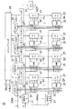
図1は、本発明に係るDRAMの概略構成を示している。ただし、記憶データの読み出しに係る部分のみが図示されている。図1において、11はロウアドレスバッファ、12はコラムアドレスバッファ、13は4Mビットの記憶容量を持つ2048ロウ×2048コラムの通常メモリアレイを備えた通常メモリブロック、14は32Kビットの記憶容量を持つ16ロウ×2048コラムの冗長メモリアレイを備えた冗長メモリブロック、15はセレクタである。PREは、冗長メモリブロック14へ与えられるプリチャージ信号である。
【0011】
ロウアドレスバッファ11は、外部から与えられた11ビットのアドレス信号A0 〜A10をロウアドレスRAとして入力し、該ロウアドレスRAのうちの9ビットからなる主ワードアドレスMWAと、残り2ビットからなる副ワードアドレスSWAとを、通常メモリブロック13及び冗長メモリブロック14へ供給するものである。コラムアドレスバッファ12は、続いて外部から与えられた11ビットのアドレス信号A0 〜A10をコラムアドレスCAとして入力し、該コラムアドレスCAのうちの9ビットからなる主ビットアドレスMBAと、残り2ビットからなる副ビットアドレスSBAとを、通常メモリブロック13の中のコラムデコーダへ供給する。このコラムデコーダによって1本が選択駆動される512本×4組のコラム選択線CS1〜CS4は、通常メモリブロック13と冗長メモリブロック14とに共用される。また、副ビットアドレスSBAは、冗長メモリブロック14へも供給される。セレクタ15は、通常メモリブロック13から出力された通常データ信号NDTと、冗長メモリブロック14から出力された冗長データ信号RDT及び切替信号N/Rとを受け取り、切替信号N/Rに応じて、通常データ信号NDTと冗長データ信号RDTとのいずれかをデータ信号DTとして選択的に出力するものである。
【0012】
図2は、図1中の通常メモリブロック13の内部構成を示している。図2において、21は512個の通常主ワードデコーダ(MWD1〜MWD512)、22は512本の通常主ワード線、23は4個の通常副ワードデコーダ(SWD1〜SWD4)、24は4本×4組の通常副ワード選択線、25は512×4個の通常副ワード線ドライバ、26は4本×2048組の通常副ワード線、27は512×4個の通常サブアレイ、28はコラムデコーダ、29は4組の通常コラムスイッチ・センスアンプ列(CS/SA列)、30は次段通常アンプである。
【0013】
512×4個の通常サブアレイ27は、4Mビットの記憶容量を持つ通常メモリアレイを構成するものである。すなわち、通常メモリアレイは、512行×4列のブロックに分割されている。個々の通常サブアレイ27は、各々1ビットのデータを記憶するための4ロウ×512コラムの通常メモリセルを有している。通常主ワード線22は、1個の行ブロックを構成する4個の通常サブアレイ27に対して共通に1本ずつ設けられている。通常副ワード選択線24は、1個の列ブロックを構成する512個の通常サブアレイ27に対して共通に4本ずつ設けられている。通常副ワード線26は、512×4個の通常サブアレイ27の各々が有する4ロウの通常メモリセルに接続されるように、該512×4個の通常サブアレイ27の各々に4本ずつ設けられている。個々の通常主ワードデコーダ21は、主ワードアドレスMWAに応じて、512本の通常主ワード線22のうちの対応する1本を選択するものである。個々の通常副ワードデコーダ23は、副ワードアドレスSWAに応じて、対応する4本の通常副ワード選択線24のうちの1本を選択するものである。個々の通常副ワード線ドライバ25は、図3に示すように4個のANDゲートで構成され、通常主ワード線22の選択及び通常副ワード選択線24の選択に応じて、対応する4本の通常副ワード線26のうちの1本を選択的に駆動するものである。この結果、主ワードアドレスMWA及び副ワードアドレスSWAからなるロウアドレスRAに応じて、通常メモリアレイの中の1ロウを構成する512×4個の通常メモリセルの各々から1ビットの記憶データがビット線上に読み出される。このようにして読み出された512×4ビットの記憶データは、通常コラムスイッチ・センスアンプ列29へ供給される。コラムデコーダ28は、主ビットアドレスMBA及び副ビットアドレスSBAからなるコラムアドレスCAに応じた1ビットの記憶データが通常コラムスイッチ・センスアンプ列29から次段通常アンプ30へ供給されるように、512本×4組のコラム選択線CS1〜CS4のうちの1本を選択するものである。次段通常アンプ30は、通常データ信号NDTを図1のセレクタ15へ供給するものである。なお、図2中の4組の通常コラムスイッチ・センスアンプ列29は、実際には、接続可能なビット線長に限界があるので、それぞれビット線方向に分割配置される。
【0014】
図4は、図1中の冗長メモリブロック14の内部構成を示している。図4において、40は冗長制御回路、41は4個の冗長主ワードデコーダ(MWD1〜MWD4)、42は4本の冗長主ワード線、43は4個の冗長副ワードデコーダ(SWD1〜SWD4)、44は4本×4組の冗長副ワード選択線、45は4×4個の冗長副ワード線ドライバ、46は4本×16組の冗長副ワード線、47は4×4個の冗長サブアレイ、49は4組の冗長コラムスイッチ・センスアンプ列(CS/SA列)、50は次段冗長アンプである。
【0015】
4×4個の冗長サブアレイ47は、32Kビットの記憶容量を持つ冗長メモリアレイを構成するものである。すなわち、冗長メモリアレイは、4行×4列のブロックに分割されている。個々の冗長サブアレイ47は、各々1ビットのデータを記憶するための4ロウ×512コラムの冗長メモリセルを有している。冗長主ワード線42は、1個の行ブロックを構成する4個の冗長サブアレイ47に対して共通に1本ずつ設けられている。冗長副ワード選択線44は、1個の列ブロックを構成する4個の冗長サブアレイ47に対して共通に4本ずつ設けられている。冗長副ワード線46は、4×4個の冗長サブアレイ47の各々が有する4冗長ロウの冗長メモリセルに接続されるように、該4×4個の冗長サブアレイ47の各々に4本ずつ設けられている。冗長制御回路40は、主ワードアドレスMWA、副ワードアドレスSWA、副ビットアドレスSBA及びプリチャージ信号PREを受け取り、2ビットの冗長主ワードアドレスMWA′、2ビットの冗長副ワードアドレスSWA′、4つのイネーブル信号EN1〜EN4及び切替信号N/Rを供給するものである。切替信号N/Rは、図1のセレクタ15へ供給される。個々の冗長主ワードデコーダ41は、冗長制御回路40から供給された冗長主ワードアドレスMWA′に応じて、4本の冗長主ワード線42のうちの対応する1本を選択するものである。個々の冗長副ワードデコーダ43は、冗長制御回路40から供給された冗長副ワードアドレスSWA′に応じて、対応する4本の冗長副ワード選択線44のうちの1本を選択するものである。同一の分割位置(同一の列ブロック位置)にある通常副ワードデコーダ23と冗長副ワードデコーダ43とは、独立に動作させることができるようになっている。しかも、イネーブル信号EN1〜EN4に応じて、4個の冗長副ワードデコーダ43のうちの1個のみが動作するようになっている。個々の冗長副ワード線ドライバ45は、図3の通常副ワード線ドライバ25と同様の4個のANDゲートで構成され、冗長主ワード線42の選択及び冗長副ワード選択線44の選択に応じて、対応する4本の冗長副ワード線46のうちの1本を選択的に駆動するものである。この結果、冗長制御回路40からそれぞれ供給された冗長主ワードアドレスMWA′及び冗長副ワードアドレスSWA′に応じて、冗長メモリアレイの中の1冗長ロウの4分の1を構成する512個の冗長メモリセルの各々から1ビットの記憶データが読み出される。このようにして読み出された512ビットの記憶データは、対応する冗長コラムスイッチ・センスアンプ列49へ供給される。そして、図2のコラムデコーダ28によって512本×4組のコラム選択線CS1〜CS4の中からいずれのコラム選択線が選択されたかに応じて、与えられたコラムアドレスCAに応じた1ビットの記憶データが冗長コラムスイッチ・センスアンプ列49から次段冗長アンプ50へ供給される。次段通常アンプ50は、冗長データ信号RDTを図1のセレクタ15へ供給するものである。
【0016】
図5は、図4中の冗長制御回路40の内部構成を示している。図5において、61は欠陥ロウアドレス検知ヒューズ回路、62は冗長主ワードアドレスヒューズ回路、63は冗長副ワードアドレスヒューズ回路、64は分割位置アドレスヒューズ回路、65は副ワードデコーダ制御回路、66は比較器である。欠陥ロウアドレス検知ヒューズ回路61と、冗長主ワードアドレスヒューズ回路62と、冗長副ワードアドレスヒューズ回路63と、分割位置アドレスヒューズ回路64とは、1組の冗長ヒューズ回路を構成している。この冗長ヒューズ回路を構成する4個のヒューズ回路61,62,63,64には、それぞれプリチャージ信号PREが供給される。図5の冗長制御回路40は、4本×2048組の通常副ワード線26のうちの予測欠陥数に応じた数の冗長ヒューズ回路を備えている。
【0017】
個々の欠陥ロウアドレス検知ヒューズ回路61は、通常メモリアレイ中の欠陥ロウの位置を示す11ビットの欠陥ロウアドレスを記憶するためのヒューズを有し、与えられたロウアドレスRAすなわち主ワードアドレスMWAと副ワードアドレスSWAとからなる11ビットのアドレスがヒューズに記憶された欠陥ロウアドレスと一致した場合には“H”レベルの欠陥ロウ検知信号REDを生成するものである。個々の冗長主ワードアドレスヒューズ回路62は、欠陥ロウアドレスに対応した2ビットの冗長主ワードアドレスMWA′を記憶するためのヒューズを有し、対応する欠陥ロウアドレス検知ヒューズ回路61が“H”レベルの欠陥ロウ検知信号REDを生成した場合にはヒューズに記憶された冗長主ワードアドレスMWA′を供給するものである。個々の冗長副ワードアドレスヒューズ回路63は、欠陥ロウアドレスに対応した2ビットの冗長副ワードアドレスSWA′を記憶するためのヒューズを有し、対応する欠陥ロウアドレス検知ヒューズ回路61が“H”レベルの欠陥ロウ検知信号REDを生成した場合にはヒューズに記憶された冗長副ワードアドレスSWA′を供給するものである。個々の分割位置アドレスヒューズ回路64は、欠陥ロウアドレスに係る通常副ワード線の欠陥位置に対応して1個の列ブロックの位置を指定するように2ビットの分割位置アドレスDPAを記憶するためのヒューズを有し、対応する欠陥ロウアドレス検知ヒューズ回路61が“H”レベルの欠陥ロウ検知信号REDを生成した場合にはヒューズに記憶された分割位置アドレスDPAを供給するものである。副ワードデコーダ制御回路65は、複数の分割位置アドレスヒューズ回路64のうちのいずれかから供給された分割位置アドレスDPAに応じて、4個の冗長副ワードデコーダ43のうちの分割位置アドレスDPAで指定された位置の1個の列ブロックに対応した1個の冗長副ワードデコーダのみを動作させるように、イネーブル信号EN1〜EN4を供給するものである。比較器66は、複数の欠陥ロウアドレス検知ヒューズ回路61のうちのいずれかが欠陥ロウ検知信号REDを生成し、かつ複数の分割位置アドレスヒューズ回路64のうちのいずれかから供給された分割位置アドレスDPAと、与えられたコラムアドレスCAのうちの列ブロック位置指定部分すなわち副ビットアドレスSBAとが一致した場合には救済が必要であることを示す“H”レベルの切替信号N/Rを、その他の場合には救済が必要でないことを示す“L”レベルの切替信号N/Rをそれぞれ供給するものである。
【0018】
図6は、図5中の欠陥ロウアドレス検知ヒューズ回路61の内部構成を示している。図6において、71は22本のヒューズからなるヒューズ列、72はNMOSトランジスタ列、73はインバータ列、74及び77はPMOSトランジスタ、75及び76はインバータである。ヒューズ列71は、22本のヒューズの切断パターンに応じて、11ビットの欠陥ロウアドレスを相補形式で記憶するものである。プリチャージ信号PREが与えられると、PMOSトランジスタ74がターンオンする結果、ノードN1が“H”レベルにプリチャージされる。与えられたロウアドレスRAすなわち主ワードアドレスMWAと副ワードアドレスSWAとからなる11ビットのアドレスがヒューズ列71に記憶された欠陥ロウアドレスと一致した場合には、ノードN1が“H”レベルに保持されるので、欠陥ロウ検知信号REDの論理レベルが“H”となる。一致しない場合には、NMOSトランジスタ列72の中のいずれかのトランジスタを通してノードN1の電荷がグラウンドに引き抜かれる結果、欠陥ロウ検知信号REDの論理レベルが“L”となる。
【0019】
図7は、図5中の冗長主ワードアドレスヒューズ回路62の内部構成を示している。図7において、101及び102は単位ヒューズ回路、103はインバータ、104及び105はCMOSトランスファゲートである。単位ヒューズ回路101,102の各々は、1本のヒューズ81と、1個のNMOSトランジスタ82と、2個のPMOSトランジスタ84,87と、1個のインバータ85とで構成される。CMOSトランスファゲート104,105の各々は、NMOSトランジスタ91と、PMOSトランジスタ92とで構成される。2本のヒューズ81は、2ビットの冗長主ワードアドレスMWA′を記憶するものである。プリチャージ信号PREが与えられると、個々の単位ヒューズ回路101,102の中のPMOSトランジスタ84がターンオンする結果、ノードN2及びN3がいずれも“H”レベルにプリチャージされる。そして、対応する欠陥ロウアドレス検知ヒューズ回路61から“H”レベルの欠陥ロウ検知信号REDが供給されると、2本のヒューズ81の切断パターンに応じた2ビットの冗長主ワードアドレスMWA′がCMOSトランスファゲート104,105に与えられる。CMOSトランスファゲート104,105は、“H”レベルの欠陥ロウ検知信号REDに応答してターンオンし、与えられた冗長主ワードアドレスMWA′を出力する。なお、図5中の冗長副ワードアドレスヒューズ回路63と、分割位置アドレスヒューズ回路64とは、図7の冗長主ワードアドレスヒューズ回路62と同一の内部構成を備えている。
【0020】
次に、上記構成を備えたDRAMの読み出し動作について説明する。ここで、図2の通常メモリアレイ中の2048ロウのうち通常副ワード線P1,P2,P3,P4で示されたロウが欠陥ロウであり、このうち実際に欠陥があるのは通常副ワード線P3のみであって、他の通常副ワード線P1,P2,P4には欠陥がないものとする。また、通常副ワード線Q1,Q2,Q3,Q4で示されたロウが欠陥ロウであり、このうち実際に欠陥があるのは通常副ワード線Q2のみであって、他の通常副ワード線Q1,Q3,Q4には欠陥がないものとする。図4の冗長メモリアレイ中の16冗長ロウのうち冗長副ワード線R1,R2,R3,R4で示された冗長ロウは、欠陥のある通常副ワード線P3及びQ2の救済に用いられるロウである。すなわち、冗長副ワード線R3は列ブロック位置(分割位置)を同じくする通常副ワード線P3の救済に、冗長副ワード線R2は列ブロック位置(分割位置)を同じくする通常副ワード線Q2の救済にそれぞれ用いられるものとする。
【0021】
まず、欠陥のある通常副ワード線P3の置換先が冗長副ワード線R3になるように、図5中の1組の冗長ヒューズ回路が予めプログラムされる。具体的には、通常副ワード線P1,P2,P3,P4に係る11ビットの欠陥ロウアドレスが欠陥ロウアドレス検知ヒューズ回路61に記憶され、冗長副ワード線R1,R2,R3,R4に対応した冗長主ワード線42に係る2ビットの冗長主ワードアドレスMWA′が冗長主ワードアドレスヒューズ回路62に記憶され、4本の冗長副ワード選択線44のうちの冗長副ワード線R1,R2,R3,R4に対応した1本の副ワード選択線に係る2ビットの冗長副ワードアドレスSWA′が冗長副ワードアドレスヒューズ回路63に記憶され、通常副ワード線P3及び冗長副ワード線R3の列ブロック位置を示す2ビットの分割位置アドレスDPAすなわち“11(2進数)”が分割位置アドレスヒューズ回路64に記憶される。また、欠陥のある通常副ワード線Q2の置換先が冗長副ワード線R2になるように、図5中の他の1組の冗長ヒューズ回路が予めプログラムされる。具体的には、通常副ワード線Q2及び冗長副ワード線R2の列ブロック位置を示す2ビットのアドレス“10(2進数)”が分割位置アドレスヒューズ回路64に記憶される点を除いて、通常副ワード線P3及び冗長副ワード線R3に係るプログラミングと同様のプログラミングが行なわれる。
【0022】
通常副ワード線P1,P2,P3,P4に係る欠陥ロウアドレスと一致するロウアドレスRAが、11ビットのアドレス信号A0 〜A10として、図1のDRAMに与えられたものとする。続いて、コラムアドレスCAが11ビットのアドレス信号A0 〜A10として同DRAMに与えられる。
【0023】
通常メモリブロック13では、主ワードアドレスMWAに対応した1本の通常主ワード線22が通常主ワードデコーダ21により選択され、各々4本の通常副ワード選択線24のうちの副ワードアドレスSWAに応じた1本の通常副ワード選択線が4個の通常副ワードデコーダ23(SWD1〜SWD4)によりそれぞれ選択され、通常副ワード線P1,P2,P3,P4が4個の通常副ワード線ドライバ25により駆動される。この結果、通常副ワード線P1,P2,P3,P4に係る欠陥ロウに属する512×4個の通常メモリセルの各々から1ビットの記憶データが読み出される。通常コラムスイッチ・センスアンプ列29は、コラムデコーダ28と協働して、コラムアドレスCAに応じた1ビットの記憶データを次段通常アンプ30へ供給する。この結果、通常データ信号NDTがセレクタ15へ供給される。この際、コラムアドレスCAが欠陥のない通常副ワード線P1,P2,P4に係る列ブロックの位置を指定するアドレスである場合には例外なく正しい通常データ信号NDTがセレクタ15へ供給されるが、コラムアドレスCAが欠陥のある通常副ワード線P3に係る列ブロックの位置を指定するアドレスである場合には不正の通常データ信号NDTがセレクタ15へ供給されることがある。
【0024】
一方、冗長メモリブロック14では、冗長制御回路40が冗長主ワードアドレスMWA′、冗長副ワードアドレスSWA′、イネーブル信号EN1〜EN4及び切替信号N/Rを供給する。詳細には、通常副ワード線P1,P2,P3,P4に係る欠陥ロウアドレスを記憶した欠陥ロウアドレス検知ヒューズ回路61が“H”レベルの欠陥ロウ検知信号REDを生成し、これに対応した冗長主ワードアドレスヒューズ回路62と、冗長副ワードアドレスヒューズ回路63と、分割位置アドレスヒューズ回路64とがそれぞれヒューズに記憶された冗長主ワードアドレスMWA′と、冗長副ワードアドレスSWA′と、“11(2進数)”の分割位置アドレスDPAとを供給する。副ワードデコーダ制御回路65は、“11(2進数)”の分割位置アドレスDPAに応じて、4つのイネーブル信号EN1〜EN4のうちの1つのイネーブル信号EN3のみをアサートする。比較器66は、分割位置アドレスヒューズ回路64から供給された分割位置アドレスDPAと、与えられたコラムアドレスCAのうちの副ビットアドレスSBAとが一致した場合には救済が必要であることを示す“H”レベルの切替信号N/Rを、その他の場合には救済が必要でないことを示す“L”レベルの切替信号N/Rをそれぞれセレクタ15へ供給する。
【0025】
更に、冗長メモリブロック14では、冗長制御回路40から供給された冗長主ワードアドレスMWA′に対応した1本の冗長主ワード線42が冗長主ワードデコーダ41により選択される。また、4個の冗長副ワードデコーダ43(SWD1〜SWD4)のうちアサートされたイネーブル信号EN3を受け取った1個の冗長副ワードデコーダ(SWD3)のみが動作して、対応する4本の冗長副ワード選択線44のうち冗長制御回路40から供給された副ワードアドレスSWA′に応じた1本の冗長副ワード選択線が選択される。この結果、1冗長ロウを構成する4本の冗長副ワード線R1,R2,R3,R4のうちの1本の冗長副ワード線R3のみが冗長副ワード線ドライバ45により駆動され、該駆動された冗長副ワード線R3に係る512個の冗長メモリセルの各々から1ビットの記憶データが読み出される。冗長コラムスイッチ・センスアンプ列49は、コラムデコーダ28と協働して、コラムアドレスCAに応じた1ビットの記憶データを次段冗長アンプ50へ供給する。この際、コラムアドレスCAが冗長副ワード線R3に係る列ブロックの位置を指定するアドレスである場合には、例外なく正しい冗長データ信号RDTがセレクタ15へ供給される。
【0026】
以上のようにして通常データ信号NDTと、冗長データ信号RDTと、切替信号N/Rとがセレクタ15に供給されると、セレクタ15は、切替信号N/Rに応じて、通常データ信号NDTと冗長データ信号RDTとのいずれかをデータ信号DTとして選択的に出力する。詳細には、コラムアドレスCAが欠陥のない通常副ワード線P1,P2,P4に係る列ブロックの位置を指定するアドレスである場合には、救済が必要でないことを示す“L”レベルの切替信号N/Rが供給される結果、通常データ信号NDTがデータ信号DTとして選択される。また、コラムアドレスCAが欠陥のある通常副ワード線P3に係る列ブロックの位置を指定するアドレスである場合には、救済が必要であることを示す“H”レベルの切替信号N/Rが供給される結果、冗長データ信号RDTがデータ信号DTとして選択される。つまり、与えられたロウアドレスRAが欠陥ロウの位置を指定するアドレスである場合には、続いて与えられたコラムアドレスCAに応じて、欠陥ロウの中の欠陥のない通常副ワード線P1,P2,P4はそのまま使用され、欠陥ロウの中の欠陥のある通常副ワード線P3のみが冗長副ワード線R3に置換されるのである。
【0027】
通常副ワード線Q1,Q2,Q3,Q4に係る欠陥ロウアドレスと一致するロウアドレスRAが図1のDRAMに与えられたときには、続いて与えられたコラムアドレスCAに応じて、欠陥ロウの中の欠陥のない通常副ワード線Q1,Q3,Q4はそのまま使用され、欠陥ロウの中の欠陥のある通常副ワード線Q2のみが冗長副ワード線R2に置換される。これから容易に類推できるように、最大4欠陥ロウを1冗長ロウで救済できる。
【0028】
なお、与えられたロウアドレスRAが無欠陥ロウの位置を指定するアドレスである場合には、いずれの欠陥ロウドレス検知ヒューズ回路61も“H”レベルの欠陥ロウ検知信号REDを生成しないので、比較器66は、分割位置アドレスヒューズ回路64のプログラミング内容にかかわらず、救済が必要でないことを示す“L”レベルの切替信号N/Rをセレクタ15へ供給する。したがって、セレクタ15は、ロウアドレスRA及びコラムアドレスCAに応じて通常メモリブロック13から供給された通常データ信号NDTを、データ信号DTとして選択する。
【0029】
以上説明してきたとおり、上記DRAMによれば、欠陥ロウの中の実際に欠陥を持つ通常副ワード線のみを同一分割位置(同一の列ブロック位置)にある冗長副ワード線に置換することとしたので、副ワード線単位でロウの置換を行なえる結果、冗長救済効率が改善される。従来は主ワード線単位でロウの置換が行なわれていたことを考えると、Kを列ブロック数(上記の例ではK=4)とすると、冗長救済効率が最大K倍に改善される。
【0030】
しかも、上記DRAMによれば、記憶された分割位置アドレスDPAに応じて4個の冗長副ワードデコーダ43(SWD1〜SWD4)のうちの所要の1個(例えば欠陥のある通常副ワード線P3の置換先である冗長副ワード線R3に係る冗長副ワードデコーダSWD3)のみが動作するように該4個の冗長副ワードデコーダ43を制御するための副ワードデコーダ制御回路65を備えた構成を採用したので、冗長副ワード選択線44及び冗長副ワード線46の駆動電流が低減される。なお、記憶された分割位置アドレスDPAに応じて4個の通常副ワードデコーダ23(SWD1〜SWD4)のうちの1個(例えば欠陥のある通常副ワード線P3に係る通常副ワードデコーダSWD3)のみが動作しないように該4個の通常副ワードデコーダ23を副ワードデコーダ制御回路65で更に制御するようにすれば、冗長メモリブロック14を備えない場合と同程度までワード線駆動電流が低減される。ただし、副ワードデコーダ制御回路65の配設を省略しても、冗長救済効率の改善効果に変わりはない。
【0031】
また、上記DRAMによれば、個々の冗長ヒューズ回路において、欠陥ロウアドレス検知ヒューズ回路61の出力すなわち欠陥ロウ検知信号REDに基づいて、冗長主ワードアドレスヒューズ回路62、冗長副ワードアドレスヒューズ回路63及び分割位置アドレスヒューズ回路64の各々の記憶情報を読み出すこととしたので、欠陥の多い分割位置に多数組の冗長ヒューズ回路を割り当てるなど、柔軟なヒューズ・プログラミングが可能になる。つまり、冗長制御回路40の中のヒューズを有効に利用できる。ただし、冗長ヒューズ回路と冗長主ワード線との対応関係が固定されるという制約が生じるけれども、冗長主ワードアドレスヒューズ回路62の配設を省略することにより冗長制御回路40の中のヒューズの数を低減してもよい。冗長副ワードアドレスヒューズ回路63についても同様である。
【0032】
なお、1欠陥ロウ中の複数の通常副ワード線に欠陥がある場合に対応するためには、分割位置アドレスヒューズ回路64の中のヒューズの数を増やせばよい。例えば、4本のヒューズの各々が異なる分割位置アドレスを表わすこととすれば、図2中の通常副ワード線P1,P2,P3,P4で示されたロウの中の複数の通常副ワード線(例えばP3及びP4)に欠陥がある場合でも、副ワード線単位のロウの置換が可能になる。
【0033】
【発明の効果】
以上説明してきたとおり、本発明によれば、階層型ワード線構造をとるアドレスマルチプレクス入力型の半導体記憶装置において副ワード線単位でロウの置換を行なうこととしたので、該半導体記憶装置の冗長救済効率が改善される。
【図面の簡単な説明】
【図1】本発明に係るDRAMの概略構成を示すブロック図である。
【図2】図1中の通常メモリブロックの内部構成を示すブロック図である。
【図3】図2中の通常副ワード線ドライバの内部構成を示す図である。
【図4】図1中の冗長メモリブロックの内部構成を示すブロック図である。
【図5】図4中の冗長制御回路の内部構成を示すブロック図である。
【図6】図5中の欠陥ロウアドレス検知ヒューズ回路の内部構成を示す図である。
【図7】図5中の冗長主ワードアドレスヒューズ回路の内部構成を示す図である。
【符号の説明】
11 ロウアドレスバッファ
12 コラムアドレスバッファ
13 通常メモリブロック
14 冗長メモリブロック
15 セレクタ
21 通常主ワードデコーダ
22 通常主ワード線
23 通常副ワードデコーダ
24 通常副ワード選択線
25 通常副ワード線ドライバ
26 通常副ワード線
27 通常サブアレイ
28 コラムデコーダ
29 通常コラムスイッチ・センスアンプ列
30 次段通常アンプ
40 冗長制御回路
41 冗長主ワードデコーダ
42 冗長主ワード線
43 冗長副ワードデコーダ
44 冗長副ワード選択線
45 冗長副ワード線ドライバ
46 冗長副ワード線
47 冗長サブアレイ
49 冗長コラムスイッチ・センスアンプ列
50 次段冗長アンプ
61 欠陥ロウアドレス検知ヒューズ回路
62 冗長主ワードアドレスヒューズ回路
63 冗長副ワードアドレスヒューズ回路
64 分割位置アドレスヒューズ回路
65 副ワードデコーダ制御回路
66 比較器
71 ヒューズ列
72 NMOSトランジスタ列
73 インバータ列
74,77 PMOSトランジスタ
75,76 インバータ
81 ヒューズ
82 NMOSトランジスタ
84,87 PMOSトランジスタ
85 インバータ
91 NMOSトランジスタ
92 PMOSトランジスタ
101,102 単位ヒューズ回路
103 インバータ
104,105 CMOSトランスファゲート
A0 〜A10 アドレス信号
CA コラムアドレス
CS1〜CS4 コラム選択線
DT データ信号
DPA 分割位置アドレス
EN1〜EN4 イネーブル信号
MBA 主ビットアドレス
MWA 主ワードアドレス
MWA′ 冗長主ワードアドレス
N1〜N3 ノード
NDT 通常データ信号
N/R 切替信号
P1〜P4 欠陥ロウの通常副ワード線
PRE プリチャージ信号
Q1〜Q4 欠陥ロウの通常副ワード線
R1〜R4 置換先の冗長副ワード線
RA ロウアドレス
RDT 冗長データ信号
RED 欠陥ロウ検知信号
SBA 副ビットアドレス
SWA 副ワードアドレス
SWA′ 冗長副ワードアドレス[0001]
BACKGROUND OF THE INVENTION
The present invention relates to an improvement in redundancy relief efficiency in an address multiplex input type semiconductor memory device having a hierarchical word line structure.
[0002]
[Prior art]
In a DRAM (Dynamic Random Access Memory) which is one of semiconductor memory devices, the storage capacity tends to increase more and more. In response to this, in order to reduce the number of terminals, a multiplex system is adopted in which addresses are divided and input into row addresses and column addresses. In such a conventional address multiplex input type DRAM, in order to improve the yield, when a given row address is an address designating the position of a defective row, one normal word related to the defective row is used. A redundant relief system has been adopted in which a line is replaced with one redundant word line corresponding thereto.
[0003]
Recently, a hierarchical word line structure has been proposed in order to reduce the wiring pitch in the DRAM (see Japanese Patent Laid-Open No. Hei 6-195964). In this case, the word lines are configured in two layers of a main word line and a sub word line. A memory array for storing data is divided into a plurality of subarray blocks, and a main word line is provided in common to the plurality of subarray blocks. A plurality of sub word selection lines and sub word lines are provided for each of the plurality of sub array blocks. One main word line is selected according to the main word address consisting of a part of the given row address, and for each sub-array block according to the sub word address consisting of the other part of the given row address One sub-word selection line is selected, and one sub-word line is selected for each sub-array block in accordance with the selection of the main word line and the selection of the sub-word selection line. Then, one memory cell is selected from one row of memory cells selected by the main word address and the sub word address in the memory array, according to the column address subsequently given. ing. Even in a DRAM having such a hierarchical word line structure, conventionally, the above-described redundancy relief scheme has been followed. That is, when the given row address is an address designating the position of the defective row, one normal main word line related to the defective row is replaced with one redundant main word line corresponding thereto. (See JP-A-6-196656).
[0004]
[Problems to be solved by the invention]
Even if a given row address is an address specifying the position of a defective row, not all memory cells of one row selected by the main word address and the sub word address have a defect, but a memory cell having a defect Is a minority. That is, even in a defective row, a sub word line related to a memory cell having a defect and a sub word line not related to a memory cell having a defect are mixed.
[0005]
However, in the conventional DRAM, since row replacement is performed in units of main word lines as described above, a defect-free sub word line is repaired at the same time as a defective sub word line, and redundancy repair efficiency is not increased. There was a problem.
[0006]
An object of the present invention is to improve redundancy relief efficiency in an address multiplex input type semiconductor memory device having a hierarchical word line structure.
[0007]
[Means for Solving the Problems]
In order to achieve the above object, according to the present invention, row replacement is performed in units of sub word lines in an address multiplex input type semiconductor memory device having a hierarchical word line structure. That is, when the given row address is an address designating the position of the defective row, the sub-word line having no defect in the defective row is used as it is and the defective row is used according to the given column address. Only the defective sub-word line is replaced with a redundant sub-word line.
[0008]
Specifically, the present invention employs a configuration including the following normal memory block, redundant memory block, and selector. That is, the normal memory block supplies storage data read from normal memory cells corresponding to a given row address. The redundant memory block has a defective row address indicating the position of the defective row in the normal memory block and at least one division position address for designating the position of at least one column block corresponding to the defective row address. The stored row address matches the stored defective row address, and the column block position designation portion of the supplied column address matches one of the stored divided position addresses In this case, the storage data read from the redundant memory cell designated by the redundant sub word line located at the same division position as the defective normal sub word line is supplied. The selector selectively outputs either storage data read from the normal memory cell or storage data read from the redundant memory cell.
[0009]
DETAILED DESCRIPTION OF THE INVENTION
Specific examples of the semiconductor memory device according to the present invention will be described below with reference to the drawings.
[0010]
FIG. 1 shows a schematic configuration of a DRAM according to the present invention. However, only the portion related to reading of stored data is shown. In FIG. 1, 11 is a row address buffer, 12 is a column address buffer, 13 is a normal memory block having a normal memory array of 2048 rows × 2048 columns having a storage capacity of 4 Mbits, and 14 has a storage capacity of 32 Kbits. A redundant memory block having a redundant memory array of 16 rows × 2048 columns, 15 is a selector. PRE is a precharge signal applied to the
[0011]
The
[0012]
FIG. 2 shows the internal configuration of the
[0013]
The 512 × 4
[0014]
FIG. 4 shows the internal configuration of the
[0015]
The 4 × 4
[0016]
FIG. 5 shows the internal configuration of the
[0017]
Each defective row address
[0018]
FIG. 6 shows the internal configuration of the defective row address
[0019]
FIG. 7 shows an internal configuration of the redundant main word
[0020]
Next, a read operation of the DRAM having the above configuration will be described. Here, of the 2048 rows in the normal memory array of FIG. 2, the rows indicated by the normal sub word lines P1, P2, P3, and P4 are defective rows, of which the normal sub word lines are actually defective. Assume that only P3 and other normal sub-word lines P1, P2, and P4 are free from defects. The rows indicated by the normal sub word lines Q1, Q2, Q3, and Q4 are defective rows. Of these, only the normal sub word line Q2 is actually defective, and other normal sub word lines Q1. , Q3, Q4 are assumed to be free of defects. Of the 16 redundant rows in the redundant memory array of FIG. 4, the redundant rows indicated by the redundant sub word lines R1, R2, R3, and R4 are used for relieving defective normal sub word lines P3 and Q2. . That is, the redundant sub-word line R3 is used to relieve the normal sub-word line P3 having the same column block position (divided position), and the redundant sub-word line R2 is used to relieve the normal sub-word line Q2 having the same column block position (divided position). Shall be used respectively.
[0021]
First, a set of redundant fuse circuits in FIG. 5 is preprogrammed so that the replacement destination of the defective normal subword line P3 becomes the redundant subword line R3. Specifically, the 11-bit defective row address related to the normal sub word lines P1, P2, P3, and P4 is stored in the defective row address
[0022]
A row address RA that matches the defective row address associated with the normal sub-word lines P1, P2, P3, P4 is an 11-bit address signal A. 0 ~ A Ten As shown in FIG. Subsequently, the column address CA is an 11-bit address signal A. 0 ~ A Ten Is given to the DRAM.
[0023]
In the
[0024]
On the other hand, in the
[0025]
Further, in the
[0026]
When the normal data signal NDT, the redundant data signal RDT, and the switching signal N / R are supplied to the
[0027]
When a row address RA that coincides with a defective row address associated with normal sub-word lines Q1, Q2, Q3, and Q4 is applied to the DRAM of FIG. 1, the row address RA in the defective row is subsequently applied in accordance with the applied column address CA. The normal subword lines Q1, Q3, and Q4 having no defect are used as they are, and only the defective normal subword line Q2 in the defective row is replaced with the redundant subword line R2. As can be easily inferred from this, a maximum of four defective rows can be relieved with one redundant row.
[0028]
If the given row address RA is an address designating the position of a non-defective row, none of the defective row dress
[0029]
As described above, according to the DRAM, only a normal subword line having a defect in a defective row is replaced with a redundant subword line at the same division position (the same column block position). As a result, row replacement can be performed in units of sub-word lines, resulting in improved redundancy relief efficiency. Considering that row replacement is conventionally performed in units of main word lines, if K is the number of column blocks (K = 4 in the above example), the redundancy relief efficiency is improved up to K times.
[0030]
Moreover, according to the DRAM, a required one of the four redundant sub-word decoders 43 (SWD1 to SWD4) (for example, replacement of the defective normal sub-word line P3) according to the stored divided position address DPA. Since the configuration including the sub-word
[0031]
Further, according to the DRAM, in each redundant fuse circuit, based on the output of the defective row address
[0032]
In order to cope with a case where a plurality of normal sub word lines in one defective row are defective, the number of fuses in the divided position
[0033]
【The invention's effect】
As described above, according to the present invention, row replacement is performed in units of sub-word lines in an address multiplex input type semiconductor memory device having a hierarchical word line structure. Relief efficiency is improved.
[Brief description of the drawings]
FIG. 1 is a block diagram showing a schematic configuration of a DRAM according to the present invention.
2 is a block diagram showing an internal configuration of a normal memory block in FIG. 1. FIG.
FIG. 3 is a diagram showing an internal configuration of a normal sub word line driver in FIG. 2;
4 is a block diagram showing an internal configuration of a redundant memory block in FIG. 1. FIG.
FIG. 5 is a block diagram showing an internal configuration of a redundant control circuit in FIG. 4;
6 is a diagram showing an internal configuration of a defective row address detection fuse circuit in FIG. 5. FIG.
7 is a diagram showing an internal configuration of a redundant main word address fuse circuit in FIG. 5. FIG.
[Explanation of symbols]
11 Row address buffer
12 Column address buffer
13 Normal memory block
14 Redundant memory blocks
15 selector
21 Normal main word decoder
22 Normal main word line
23 Normal sub-word decoder
24 Normal sub-word selection line
25 Normal sub-word line driver
26 Normal sub-word line
27 Normal subarray
28 Column decoder
29 Normal column switch / sense amplifier array
30 Next stage normal amplifier
40 Redundant control circuit
41 Redundant main word decoder
42 Redundant main word line
43 Redundant sub-word decoder
44 Redundant subword selection line
45 Redundant sub word line driver
46 Redundant sub-word line
47 Redundant subarrays
49 Redundant column switch / sense amplifier array
50th stage redundant amplifier
61 Defective row address detection fuse circuit
62 Redundant main word address fuse circuit
63 Redundant sub-word address fuse circuit
64 division position address fuse circuit
65 Sub-word decoder control circuit
66 Comparator
71 Fuse row
72 NMOS transistor array
73 Inverter train
74, 77 PMOS transistor
75,76 inverter
81 fuse
82 NMOS transistor
84,87 PMOS transistor
85 inverter
91 NMOS transistor
92 PMOS transistor
101,102 unit fuse circuit
103 inverter
104,105 CMOS transfer gate
A 0 ~ A Ten Address signal
CA column address
CS1-CS4 Column selection line
DT data signal
DPA division position address
EN1-EN4 enable signal
MBA main bit address
MWA main word address
MWA 'Redundant main word address
N1-N3 nodes
NDT Normal data signal
N / R switching signal
P1-P4 Normal sub-word line of defective row
PRE precharge signal
Q1-Q4 Normal sub word line of defective row
R1-R4 Redundant sub-word lines to be replaced
RA row address
RDT redundant data signal
RED Defect low detection signal
SBA sub-bit address
SWA Subword address
SWA 'Redundant sub-word address
Claims (4)
各々データを記憶するためのLロウ(Lは整数)の通常メモリセルをそれぞれ有するJ×K個(J,Kは整数)の通常サブアレイで構成されるように、J行K列のブロックに分割された通常メモリアレイと、
各々前記通常メモリアレイのうちの1個の行ブロックを構成するK個の通常サブアレイに対して共通に1本ずつ設けられたJ本の通常主ワード線と、
各々前記通常メモリアレイのうちの1個の列ブロックを構成するJ個の通常サブアレイに対して共通にL本ずつ設けられたK組の通常副ワード選択線と、
前記J×K個の通常サブアレイの各々が有するLロウの通常メモリセルに接続されるように、前記J×K個の通常サブアレイの各々にL本ずつ設けられたJ×K組の通常副ワード線と、
与えられたロウアドレスの一部からなる主ワードアドレスに応じて、前記J本の通常主ワード線のうちの1本を選択するための通常主ワードデコーダ手段と、
各々前記与えられたロウアドレスの他の部分からなる副ワードアドレスに応じて、前記K組の通常副ワード選択線のうちの対応する1組を構成するL本の通常副ワード選択線のうちの1本をそれぞれ選択するためのK個の通常副ワードデコーダと、
各々前記通常主ワード線の選択及び前記通常副ワード選択線の選択に応じて、前記J×K組の通常副ワード線のうちの対応する1組を構成するL本の通常副ワード線のうちの1本をそれぞれ選択的に駆動するためのJ×K個の通常副ワード線ドライバと、
各々データを記憶するためのNロウ(Nは整数)の冗長メモリセルをそれぞれ有するM×K個(Mは整数)の冗長サブアレイで構成されるように、M行K列のブロックに分割された冗長メモリアレイと、
各々前記冗長メモリアレイのうちの1個の行ブロックを構成するK個の冗長サブアレイに対して共通に1本ずつ設けられたM本の冗長主ワード線と、
各々前記冗長メモリアレイのうちの1個の列ブロックを構成するM個の冗長サブアレイに対して共通にN本ずつ設けられたK組の冗長副ワード選択線と、
前記M×K個の冗長サブアレイの各々が有するNロウの冗長メモリセルに接続されるように、前記M×K個の冗長サブアレイの各々にN本ずつ設けられたM×K組の通常副ワード線と、
前記通常メモリアレイ中の欠陥ロウの位置を示す欠陥ロウアドレスと、該欠陥ロウアドレスに対応した冗長主ワードアドレスと、前記欠陥ロウアドレスに対応した冗長副ワードアドレスと、前記欠陥ロウアドレスに係る通常副ワード線の欠陥位置に対応して少なくとも1個の列ブロックの位置を指定するための少なくとも1つの分割位置アドレスとを記憶し、かつ前記与えられたロウアドレスが前記記憶された欠陥ロウアドレスと一致した場合には前記記憶された冗長主ワードアドレス及び冗長副ワードアドレスを供給するとともに、前記与えられたロウアドレスが前記記憶された欠陥ロウアドレスと一致しかつ与えられたコラムアドレスのうちの列ブロック位置指定部分が前記記憶された分割位置アドレスのうちの1つと一致した場合には救済が必要であることを示し、その他の場合には救済が必要でないことを示す切替信号を供給するための冗長制御回路と、
前記冗長制御回路から供給された冗長主ワードアドレスに応じて、前記M本の冗長主ワード線のうちの1本を選択するための冗長主ワードデコーダ手段と、
各々前記冗長制御回路から供給された冗長副ワードアドレスに応じて、前記K組の冗長副ワード選択線のうちの対応する1組を構成するN本の冗長副ワード選択線のうちの1本をそれぞれ選択するためのK個の冗長副ワードデコーダと、
各々前記冗長主ワード線の選択及び前記冗長副ワード選択線の選択に応じて、前記M×K組の冗長副ワード線のうちの対応する1組を構成するN本の冗長副ワード線のうちの1本をそれぞれ選択的に駆動するためのM×K個の冗長副ワード線ドライバと、
前記与えられたコラムアドレスに応じて、前記通常メモリアレイ中の前記主ワードアドレス及び前記副ワードアドレスで選択された1ロウの通常メモリセルの中から1個の通常メモリセルを、前記冗長メモリアレイ中の前記冗長主ワードアドレス及び前記冗長副ワードアドレスで選択された1ロウの冗長メモリセルの中から1個の冗長メモリセルをそれぞれ選択するためのコラムデコーダ手段と、
前記コラムデコーダ手段により選択された1個の通常メモリセルの記憶データを読み出すための手段と、
前記コラムデコーダ手段により選択された1個の冗長メモリセルの記憶データを読み出すための手段と、
救済が必要でないことを前記冗長制御回路から供給された切替信号が示す場合には前記読み出された通常メモリセルの記憶データを、救済が必要であることを前記冗長制御回路から供給された切替信号が示す場合には前記読み出された冗長メモリセルの記憶データをそれぞれ選択して出力するためのセレクタとを備えたことを特徴とする半導体記憶装置。An address multiplex input type semiconductor memory device having a hierarchical word line structure,
Divided into blocks of J rows and K columns so as to be composed of J × K normal subarrays each having L row (L is an integer) normal memory cells for storing data. A normal memory array,
J normal main word lines each provided in common to K normal sub-arrays constituting one row block of each of the normal memory arrays;
K sets of normal sub-word selection lines provided in common to J normal sub-arrays, each of which constitutes one column block of the normal memory array,
J × K sets of normal subwords provided in L in each of the J × K normal subarrays so as to be connected to the L row normal memory cells included in each of the J × K normal subarrays. Lines and,
Normal main word decoder means for selecting one of the J normal main word lines according to a main word address comprising a part of a given row address;
Of the L normal subword selection lines that constitute one corresponding set of the K sets of normal subword selection lines according to the subword address that consists of another part of the given row address. K normal sub-word decoders for selecting each one,
Of the L normal sub-word lines constituting one corresponding set of the J × K normal sub-word lines, depending on the selection of the normal main word line and the selection of the normal sub-word selection line, respectively. J × K normal sub-word line drivers for selectively driving one of each,
Each block is divided into blocks of M rows and K columns so as to be composed of M × K (M is an integer) redundant subarrays each having N rows (N is an integer) redundant memory cells for storing data. A redundant memory array;
Each of M redundant main word lines provided in common to K redundant sub-arrays constituting one row block of each of the redundant memory arrays;
K sets of redundant sub-word selection lines provided in common with respect to M redundant sub-arrays each constituting one column block of the redundant memory array;
M × K sets of normal subwords provided in each of the M × K redundant sub-arrays so as to be connected to N rows of redundant memory cells included in each of the M × K redundant sub-arrays. Lines and,
A defective row address indicating the position of a defective row in the normal memory array, a redundant main word address corresponding to the defective row address, a redundant subword address corresponding to the defective row address, and a normal related to the defective row address At least one division position address for designating the position of at least one column block corresponding to the defect position of the sub word line, and the given row address is stored in the stored defect row address If they match, the stored redundant main word address and redundant subword address are supplied, and the given row address matches the stored defective row address, and the column of the given column addresses. If the block position designation part matches one of the stored division position addresses Already indicates that it is necessary, the redundancy control circuit for supplying a switching signal indicating that it is not necessary relief otherwise,
Redundant main word decoder means for selecting one of the M redundant main word lines according to the redundant main word address supplied from the redundancy control circuit;
One of N redundant subword selection lines constituting one corresponding set of the K redundant subword selection lines is set in accordance with the redundant subword address supplied from the redundancy control circuit. K redundant subword decoders for selecting each;
Of the N redundant sub word lines that constitute one corresponding set of the M × K redundant sub word lines, depending on the selection of the redundant main word line and the redundant sub word selection line, respectively. M × K redundant sub-word line drivers for selectively driving each of
According to the given column address, one normal memory cell is selected from the one row of normal memory cells selected by the main word address and the sub word address in the normal memory array. Column decoder means for respectively selecting one redundant memory cell from one row of redundant memory cells selected by the redundant main word address and redundant subword address therein;
Means for reading storage data of one normal memory cell selected by the column decoder means;
Means for reading storage data of one redundant memory cell selected by the column decoder means;
When the switching signal supplied from the redundancy control circuit indicates that no relief is required, the switching data supplied from the redundancy control circuit indicates that the storage data of the read normal memory cell is needed. A semiconductor memory device comprising: a selector for selecting and outputting each of the read storage data of the redundant memory cell when the signal indicates.
前記冗長制御回路は、
各々欠陥ロウアドレスを記憶するためのヒューズを有し、かつ各々前記与えられたロウアドレスが前記ヒューズに記憶された欠陥ロウアドレスと一致した場合には欠陥ロウ検知信号を生成するための複数の欠陥ロウアドレス検知ヒューズ回路と、
各々冗長主ワードアドレスを記憶するためのヒューズを有し、かつ各々前記複数の欠陥ロウアドレス検知ヒューズ回路のうちの対応する欠陥ロウアドレス検知ヒューズ回路が欠陥ロウ検知信号を生成した場合には前記ヒューズに記憶された冗長主ワードアドレスを供給するための複数の冗長主ワードアドレスヒューズ回路と、
各々冗長副ワードアドレスを記憶するためのヒューズを有し、かつ各々前記複数の欠陥ロウアドレス検知ヒューズ回路のうちの対応する欠陥ロウアドレス検知ヒューズ回路が欠陥ロウ検知信号を生成した場合には前記ヒューズに記憶された冗長副ワードアドレスを供給するための複数の冗長副ワードアドレスヒューズ回路と、
各々分割位置アドレスを記憶するためのヒューズを有し、かつ各々前記複数の欠陥ロウアドレス検知ヒューズ回路のうちの対応する欠陥ロウアドレス検知ヒューズ回路が欠陥ロウ検知信号を生成した場合には前記ヒューズに記憶された分割位置アドレスを供給するための複数の分割位置アドレスヒューズ回路と、
前記複数の欠陥ロウアドレス検知ヒューズ回路のうちのいずれかが欠陥ロウ検知信号を生成し、かつ前記複数の分割位置アドレスヒューズ回路のうちのいずれかから供給された分割位置アドレスと、前記与えられたコラムアドレスのうちの列ブロック位置指定部分とが一致した場合には救済が必要であることを示し、その他の場合には救済が必要でないことを示す切替信号を供給するための比較器とを備えたことを特徴とする半導体記憶装置。The semiconductor memory device according to claim 1 .
The redundant control circuit includes:
A plurality of defects for generating a defective row detection signal each having a fuse for storing a defective row address, and each of the given row addresses coincides with a defective row address stored in the fuse A row address detection fuse circuit;
When each of the plurality of defective row address detection fuse circuits has a fuse for storing a redundant main word address, and the corresponding defective row address detection fuse circuit generates a defective row detection signal, the fuse A plurality of redundant main word address fuse circuits for supplying redundant main word addresses stored in
When each of the plurality of defective row address detection fuse circuits has a fuse for storing a redundant sub-word address, and the corresponding defective row address detection fuse circuit generates a defective row detection signal, the fuse A plurality of redundant sub-word address fuse circuits for supplying redundant sub-word addresses stored in
When each of the plurality of defective row address detection fuse circuits has a fuse for storing the divided position address and the corresponding defective row address detection fuse circuit generates a defective row detection signal, A plurality of split position address fuse circuits for supplying a stored split position address;
Any one of the plurality of defective row address detection fuse circuits generates a defective row detection signal, and the divided position address supplied from any of the plurality of divided position address fuse circuits, and the given A comparator for supplying a switching signal indicating that the repair is necessary when the column address position specifying portion of the column address matches, and in other cases the repair is not necessary A semiconductor memory device.
前記冗長制御回路は、前記複数の分割位置アドレスヒューズ回路のうちのいずれかから供給された分割位置アドレスに応じて、前記K個の冗長副ワードデコーダのうちの前記供給された分割位置アドレスで指定された位置の列ブロックに対応した冗長副ワードデコーダのみが動作するように、前記K個の冗長副ワードデコーダの各々を制御するための副ワードデコーダ制御回路を更に備えたことを特徴とする半導体記憶装置。The semiconductor memory device according to claim 2 .
The redundancy control circuit is designated by the supplied division position address of the K redundant sub-word decoders according to the division position address supplied from any of the plurality of division position address fuse circuits. And a sub-word decoder control circuit for controlling each of the K redundant sub-word decoders so that only the redundant sub-word decoder corresponding to the column block at the specified position operates. Storage device.
前記副ワードデコーダ制御回路は、前記K個の通常副ワードデコーダのうちの前記供給された分割位置アドレスで指定された位置の列ブロックに対応した通常副ワードデコーダのみが動作しないように、前記K個の通常副ワードデコーダの各々を制御する機能を更に備えたことを特徴とする半導体記憶装置。The semiconductor memory device according to claim 3 .
The sub-word decoder control circuit prevents the K sub-word decoder from operating only the normal sub-word decoder corresponding to the column block at the position specified by the supplied division position address among the K normal sub-word decoders. A semiconductor memory device further comprising a function of controlling each of the normal sub-word decoders.
Priority Applications (1)
| Application Number | Priority Date | Filing Date | Title |
|---|---|---|---|
| JP01694796A JP3797697B2 (en) | 1996-02-02 | 1996-02-02 | Semiconductor memory device |
Applications Claiming Priority (1)
| Application Number | Priority Date | Filing Date | Title |
|---|---|---|---|
| JP01694796A JP3797697B2 (en) | 1996-02-02 | 1996-02-02 | Semiconductor memory device |
Publications (2)
| Publication Number | Publication Date |
|---|---|
| JPH09213096A JPH09213096A (en) | 1997-08-15 |
| JP3797697B2 true JP3797697B2 (en) | 2006-07-19 |
Family
ID=11930332
Family Applications (1)
| Application Number | Title | Priority Date | Filing Date |
|---|---|---|---|
| JP01694796A Expired - Fee Related JP3797697B2 (en) | 1996-02-02 | 1996-02-02 | Semiconductor memory device |
Country Status (1)
| Country | Link |
|---|---|
| JP (1) | JP3797697B2 (en) |
Families Citing this family (4)
| Publication number | Priority date | Publication date | Assignee | Title |
|---|---|---|---|---|
| KR100370232B1 (en) * | 1999-04-28 | 2003-01-29 | 삼성전자 주식회사 | Redundancy circuit capable of repairing defect cell to redundancy cell repeatly |
| JP2002050191A (en) | 2000-08-02 | 2002-02-15 | Fujitsu Ltd | Semiconductor memory |
| KR100443507B1 (en) * | 2001-11-30 | 2004-08-09 | 주식회사 하이닉스반도체 | Circuit of redundancy in embedded dram |
| JP4758229B2 (en) | 2003-07-15 | 2011-08-24 | エルピーダメモリ株式会社 | Semiconductor memory device |
-
1996
- 1996-02-02 JP JP01694796A patent/JP3797697B2/en not_active Expired - Fee Related
Also Published As
| Publication number | Publication date |
|---|---|
| JPH09213096A (en) | 1997-08-15 |
Similar Documents
| Publication | Publication Date | Title |
|---|---|---|
| US6084807A (en) | Memory device with global redundancy | |
| US7079432B2 (en) | Semiconductor storage device formed to optimize test technique and redundancy technology | |
| US5469388A (en) | Row redundancy circuit suitable for high density semiconductor memory devices | |
| JP3598119B2 (en) | Redundant decoder | |
| US6519192B2 (en) | Semiconductor memory device having a large band width and allowing efficient execution of redundant repair | |
| KR100443853B1 (en) | Semiconductor memory device | |
| US5617364A (en) | Semiconductor memory device | |
| US4881200A (en) | Erasable programmable read only memory device | |
| US5469401A (en) | Column redundancy scheme for DRAM using normal and redundant column decoders programmed with defective array address and defective column address | |
| JPH0644796A (en) | Memory having column redundancy and locally arranged column redundancy control signal | |
| JPH03176899A (en) | Memory circuit | |
| JP3254432B2 (en) | Highly reliable semiconductor integrated circuit memory by selective assignment of redundant element groups to domains | |
| JPH11250688A (en) | Semiconductor storage device | |
| JPH11317093A (en) | Method and device for substituting redundancy word lines in restorable semiconductor memory device | |
| US6460110B2 (en) | Semiconductor memory | |
| JPH09147595A (en) | Semiconductor storage device | |
| JP3797697B2 (en) | Semiconductor memory device | |
| US20050024976A1 (en) | Content addressable memory device | |
| JP3626254B2 (en) | Redundant circuit device for integrated semiconductor memory | |
| US6809972B2 (en) | Circuit technique for column redundancy fuse latches | |
| JP2002050191A (en) | Semiconductor memory | |
| JP4693197B2 (en) | Semiconductor memory device | |
| JP3450621B2 (en) | Storage device and reading method | |
| EP0499131A1 (en) | High efficiency row redundancy for dynamic ram | |
| US7117400B2 (en) | Memory device with data line steering and bitline redundancy |
Legal Events
| Date | Code | Title | Description |
|---|---|---|---|
| A977 | Report on retrieval |
Free format text: JAPANESE INTERMEDIATE CODE: A971007 Effective date: 20050830 |
|
| A131 | Notification of reasons for refusal |
Free format text: JAPANESE INTERMEDIATE CODE: A131 Effective date: 20050906 |
|
| A521 | Written amendment |
Free format text: JAPANESE INTERMEDIATE CODE: A523 Effective date: 20051102 |
|
| TRDD | Decision of grant or rejection written | ||
| A01 | Written decision to grant a patent or to grant a registration (utility model) |
Free format text: JAPANESE INTERMEDIATE CODE: A01 Effective date: 20060404 |
|
| A61 | First payment of annual fees (during grant procedure) |
Free format text: JAPANESE INTERMEDIATE CODE: A61 Effective date: 20060418 |
|
| R150 | Certificate of patent or registration of utility model |
Free format text: JAPANESE INTERMEDIATE CODE: R150 |
|
| FPAY | Renewal fee payment (event date is renewal date of database) |
Free format text: PAYMENT UNTIL: 20100428 Year of fee payment: 4 |
|
| FPAY | Renewal fee payment (event date is renewal date of database) |
Free format text: PAYMENT UNTIL: 20110428 Year of fee payment: 5 |
|
| LAPS | Cancellation because of no payment of annual fees |