JP3774525B2 - Method and apparatus for measuring negative ions in plasma - Google Patents
Method and apparatus for measuring negative ions in plasma Download PDFInfo
- Publication number
- JP3774525B2 JP3774525B2 JP00017297A JP17297A JP3774525B2 JP 3774525 B2 JP3774525 B2 JP 3774525B2 JP 00017297 A JP00017297 A JP 00017297A JP 17297 A JP17297 A JP 17297A JP 3774525 B2 JP3774525 B2 JP 3774525B2
- Authority
- JP
- Japan
- Prior art keywords
- plasma
- negative
- potential
- ions
- electrode
- Prior art date
- Legal status (The legal status is an assumption and is not a legal conclusion. Google has not performed a legal analysis and makes no representation as to the accuracy of the status listed.)
- Expired - Lifetime
Links
- 150000002500 ions Chemical class 0.000 title claims description 99
- 238000000034 method Methods 0.000 title claims description 10
- 239000000758 substrate Substances 0.000 claims description 63
- 239000002245 particle Substances 0.000 claims description 26
- 238000004949 mass spectrometry Methods 0.000 claims description 10
- 238000000605 extraction Methods 0.000 claims description 5
- 238000005259 measurement Methods 0.000 description 15
- 238000004458 analytical method Methods 0.000 description 12
- 238000010586 diagram Methods 0.000 description 6
- 238000001020 plasma etching Methods 0.000 description 6
- 230000005684 electric field Effects 0.000 description 5
- 238000005530 etching Methods 0.000 description 5
- 239000012212 insulator Substances 0.000 description 4
- 238000005268 plasma chemical vapour deposition Methods 0.000 description 3
- 238000001228 spectrum Methods 0.000 description 3
- XEEYBQQBJWHFJM-UHFFFAOYSA-N Iron Chemical compound [Fe] XEEYBQQBJWHFJM-UHFFFAOYSA-N 0.000 description 2
- 230000000903 blocking effect Effects 0.000 description 2
- 239000003990 capacitor Substances 0.000 description 2
- 230000007246 mechanism Effects 0.000 description 2
- 239000013307 optical fiber Substances 0.000 description 2
- 239000004065 semiconductor Substances 0.000 description 2
- 239000000126 substance Substances 0.000 description 2
- 238000005452 bending Methods 0.000 description 1
- 230000002902 bimodal effect Effects 0.000 description 1
- 230000015572 biosynthetic process Effects 0.000 description 1
- 238000000354 decomposition reaction Methods 0.000 description 1
- 230000007423 decrease Effects 0.000 description 1
- 235000012489 doughnuts Nutrition 0.000 description 1
- 230000000694 effects Effects 0.000 description 1
- 229910052736 halogen Inorganic materials 0.000 description 1
- 150000002367 halogens Chemical class 0.000 description 1
- 229910052742 iron Inorganic materials 0.000 description 1
- 238000000691 measurement method Methods 0.000 description 1
Images


Landscapes
- Drying Of Semiconductors (AREA)
- Electron Tubes For Measurement (AREA)
Description
【0001】
【発明の属する技術分野】
本発明はブラズマを利用して、半導体上或いは電子部品、その他の基板上の物質をエッチングするエッチング装置や、基板上に他の物質を成膜するプラズマCVD装置のプラズマ中の負イオンの質量をモニターする負イオン質量分析法及び装 置に関するものである。
【0002】
【従来の技術】
例えばエッチング装置においては、ハロゲン系のガスを真空室内に導入し、交番電力或いは高周波電力を印加してプラズマを形成し、発生したイオン及びラジカルを利用して基板をエッチングする。この場合、プラズマ電位は基板及び壁面に対し常に正の電位を持っており、従って、プラズマ中で発生した正イオンは基板及び壁面に対してこの正の電位を持って基板及び壁面に対して飛行する。しかし、プラズマ中で発生した負のイオンはブラズマと基板及び壁面の間にできたシース電位により阻止され、基板及び壁面には到達することができない。このため、正イオン測定は容易であるが負イオン測定は困難である。
【0003】
添付図面の図4及び図5には従来技術によるプラズマ中のイオンエネルギー及び質量の測定法が示され、図4は、Coburn等によって報告された、接地電位となっている壁面に入射する正イオンの質量及びエネルギー分布を測定するのに使用された装置を示す(J.Appl.Phys.,43(1972)4965参照) 。
この例では、質量分析器の取り付けられている電極が接地電極になっているので、プラズマ中の正イオンはプラズマ電位と接地電位の差のエネルギーで質量分析器に入射する。
一方、図5は高周波電力が印加されている基板電極に取り付けられたエネルギー分析器付き質量分析計の例である。これらの場合にも、プラズマ電位と基板電極電位の差のエネルギーを持って基板電極に入射する正イオンを分析している。
このように正イオンは容易に基板電極に入射するので測定は容易であるが、プラズマ中の負イオンの測定は難しく殆ど報告されていない。プラズマ電位が正の電位を持っていてシースが負電荷に対して阻止電位として働くため、正イオンの測定と同じ方法では測定できない。また、多量の電子が存在することも測定を困難にしている。しかし、アフターグロー領域での負イオンの測定例は多数報告されている(例えば:L.J. Overzet, J.H. Beberman及びJ.T. Verdeyen, J. App. Phys.,66(1989) 1622, 及びA.A. Howling, J.L. Dorier 及びCh. Hollenstein, App. Phys. Lett., 62(1993)1341 参照) 。これは、アフターグロー領域ではシースが殆ど形成されていないことと電子付着により電子密度が減少し負イオン密度が増加するからと思われる。
図4のCoburn等によって報告された測定法では、質量分析器の取り付けられている電極が接地電極になっているので、プラズマ中の正イオンはプラズマ電位と接地電位の差のエネルギーで質量分析器に入射する。この方法によりプラズマCVD や陽極結合のプラズマエッチング等のように接地電位基板に入射する正イオンのエネルギー及び質量が分かり、プラズマCVD 等の成膜機構解明やプラズマエッチング等のラジカルによるエッチング機構解明には大いに有益な情報が得られている。
図5に示すものは、反応性イオンエッチングに用いられているプラズマの正イオンの測定を目的として、高周波電力が印加されている浮遊電極に取り付けられた例である。
反応性イオンエッチングでは浮遊電位基板電極に交番電場或いは高周波電場を印加し、負の自己バイアスを発生させ、プラズマ電位と基板電位とに大きな電位差を発生させて、大きな正イオンのエネルギーを得て、基板をエッチングしている。この時、基板電極は自己バイアスされた直流成分と印加されている高周波電場の交流成分で合成された電位になっている。図5の例では、イオン分析器及び質量分析器の電位は浮遊電位である基板電極の直流成分に等しくなるが、正確に基板電極の電位とは等しくならない。
【0004】
図6には先に特願平8 −77159 において提案した浮遊電極基板に入射するイオンエネルギー分析器及び質量分析器の構造を示す。図6において1はプラズマ発生室で、このプラズマ発生室1内にはプラズマ発生用電極2が配置され、このプラズマ発生用電極2はマッチングボックス3を介して高周波電源4に接続されている。プラズマ発生室1内のプラズマ発生用電極2に対向して基板電極5が絶縁碍子6を介してプラズマ発生室1に取り付けられている。基板電極5は、プラズマ発生室1内に発生するプラズマに接する位置にイオン引き込み用の開口5aを備えており、そしてコンデンサ7及びマッチングボックス8を介してバイアス用高周波電源9に接続されている。
基板電極5内にはエネルギー分析器10が配置され、このエネルギー分析器10は検出しようとするイオンエネルギーレベルより低いエネルギーのイオンをカットするメッシュ電極10a と外筒電極10b と内筒電極10c とを備えており、これらの各電極はイオンエネルギー制御電源11に接続されている。
また12は四重極型の質量分析器で、各電極は質量分析用制御電源13に接続されている。14はイオン検出器であり、質量分析器12と共に、真空容器15内に挿置されている。真空容器15は基板電極5の開放端に絶縁碍子16を介して結合されている。なお図6において17はフォトカプラー、18は光ファイバー、19は測定用回路、20は掃引電源であり、図示したように接続されている。
この構造においてはイオンエネルギー分析器10、イオンエネルギー制御電源11、質量分析器12、質量分析用制御電源13等の分析器及び制御電源を全て基板電極5に接続し、接地電位に対し浮遊電位としている。従って、基板電極5の小孔を通ってエネルギー分析器10に入り込むイオンは、基板電極5とエネルギー分析器10が同電位になっているため、何の摂動を受けることもなくエネルギー分析される。
【0005】
エネルギー分析器が基板電極の直流成分のみに等しくなる図5の例の場合には、基板電極とエネルギー分析器間に高周波成分の摂動が働く。高周波電場を飛翔するイオンのエネルギースペクトルは高周波電場の摂動を受ける時間によって加速されかたが異なり、高速側と低速側に偏る、いわゆるbimodal 形になる。基板電極とエネルギー分析器間に高周波電位が印加されていると、イオンに摂動が掛かりスペクトル形状に影響を与えると考えられる。直流電位、高周波電位とも同電位にすることでこの問題は解決され、正確なイオンのスペクトルが得られる。
一方、アフターグロー中における負イオン分析ではプラズマと分析部間にシースが形成されないので、負イオンを少しだけ引き込むための電位を印加すれば測定は可能である。しかし、ここで測定の対象としているシースが形成されているプラズマ中の負イオンの測定は、大きなシース電位があるので負イオンを引き込むことは容易ではなく、大変難しい。
【0006】
【発明が解決しようとする課題】
従来のプラズマ中のイオン種分析法は基板或いは壁面に入射する正イオンのみを対象としていた。プラズマ中で生成された正イオンはプラズマ電位と基板電位或いは通常接地電位になっている壁面電位との差で飛翔し、基板或いは壁面に入射する。プラズマ中で生成される正の電荷を持った粒子は正イオンのみであるから、測定器には正イオンのみが入射する。
一方、プラズマ中で生成される負の電荷を持った粒子には電子と負イオンがある。プラズマは基板や壁面より高い正の電位を持っているので、プラズマ中にある負の電荷を持つ粒子はプラズマ中に閉じこめられている。電子は比較的大きなエネルギー分布を持ち、高いエネルギーを持つ電子は、シースが最小になる瞬間に基板或いは壁面に到達することができる。しかし、負イオンのエネルギーは小さいので、シースを乗り越えて基板或いは壁面に到達することができない。
従って、ブラズマ中の負イオンを測定するためには、阻止電位となっているシース電位を破って負イオンを引き出さなければならない。また、シースを破って負の電荷を持った粒子を引き出したとしても、負の電荷を持つ多量の電子を除かないと負イオンを測定することはできない。
そこで本発明の目的は、上記のように従来困難であったプラズマ中の負イオンの測定を可能にする方法及び装置を提供することを目的としている。
【0007】
【課題を解決するための手段】
上記の目的を達成するために、本発明の第1の発明によれば、反応性ガスを主体とする気体を真空中に導入し、低圧で交番電力、高周波電力、マイクロ波電力等によりプラズマを形成して導入気体をプラズマ分解し、発生した原子、分子、ラジカル、イオンを利用して、プラズマに接する基板電極に装着した基板を処理する装置において、基板電極の開口を介してオリフィスを備えた負の荷電粒子引出電極をプラズマ端まで挿入し、プラズマと基板電極または壁面との間に形成されるシースを、オリフィスにプラズマ電位よりも高い電位を印加することにより微小な領域において破壊して負の荷電粒子を引き出し、引き出した負の荷電粒子の流れ方向に対して垂直方向にS極とN極とが離間して対向配置された一体の磁気回路により垂直磁場を掛けて負の荷電粒子の内電子を排除し、負イオンのみを通過させて質量分析することを特徴とするプラズマ中の負イオンの質量分析法が提供される。
【0008】
また、本発明の第2の発明によれば、プラズマを発生させるプラズマ発生室と、プラズマ発生室中のプラズマに接する位置に配置され、プラズマ中のイオンを通す開口を備えた基板電極と、基板電極の開口を通って入ってきたイオンの質量を分析する質量分析器とを有し、イオンの質量を分析するようにした装置において、プラズマと壁面または基板電極の間に形成されるシ一スを微小な領域において破壊して負の荷電粒子を引き出すためのプラズマ電位よりも高い電位を印加されると共に基板電極の開口を介してプラズマ端まで挿入されたオリフィスを備えた負の荷電粒子引出電極と、引き出した負の荷電粒子の流れ方向に対して垂直方向に、S極とN極とが離間して対向配置された一体の磁気回路により垂直磁場を形成して負の荷電粒子の内電子を排除する垂直磁場発生手段とを設けたことを特徴としている。
【0009】
各発明において好ましくは、オリフィスに印加される電位はプラズマ電位より20〜100V高くされる。
またオリフィスを通して引き出した負の荷電粒子の流入方向に対して垂直方向に掛けられる弱い垂直磁場は、好ましくは5.0×10 −3 〜2.0×10 −2 テスラである。
【0010】
【作用】
このように構成した本発明の各発明においては、負に帯電した粒子を引き込むための微小なオリフィスを持つ負の荷電粒子引出電極をプラズマ端まで挿入することで実施できるので、プラズマを乱すことがなく、また、閉じた磁気回路により弱い垂直磁場を重畳して電子のみを除くようにしているので、イオンの軌道を大きく曲げることもなく負イオンのみを分析器に導くことができ、それにより、負イオンの質量分析が可能となる。
【0011】
【発明の実施の形態】
以下、添付図面の図1〜図3に示す実施例に基づき本発明の実施の形態について説明する。
【実施例】
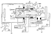
図1には本発明の一実施例によるプラズマ中の負イオンの測定装置を示す。図1において、21はプラズマ発生室で、このプラズマ発生室21内にはプラズマ発生用電極22が配置され、このプラズマ発生用電極22はマッチングボックス23を介して高周波電源24に接続されている。プラズマ発生室21内のプラズマ発生用電極22に対向して基板電極25が絶縁碍子26を介してプラズマ発生室21に取り付けられている。基板電極25は、プラズマ発生室21内に発生するプラズマに接する位置にイオン引き込み用の開口25aを備えており、そしてコンデンサ27及びマッチングボ ックス28を介してバイアス用高周波電源29に接続されている。
基板電極25内には質量分析部30が配置され、この質量分析部30は、基板電極25に隣接して設けられたイオン引込電極31と電子除去用マグネット32とイオンエネルギー制御電極33と質量分析器34とイオン検出器35とを備え、質量分析部30に印加される電圧は全て高周波印加電極を基準としている。
【0012】
イオンエネルギー制御電極33はイオンエネルギー制御電源36に接続され、質量分析器34の各電極は質量分析用制御電源37に接続され、プラズマ電位よりも5〜20eV高くなるようにしている。イオン引込電極31には電源38によりプラズマ電位よりも5O〜200eV高い電位を印加するようにされている。質量分析器34及びイオ ン検出器35は真空容器39内に挿置されている。真空容器39は基板電極25の開放端に絶縁碍子40を介して結合されている。
また図1において41はフォトカプラー、42は光ファイバー、43は測定用回路であり、図示したように接続されている。
【0013】
次に図2及び図3を参照して負イオン測定の原理について説明する。
図2に本発明による装置の電位配分を概略的に示す。V1は電源38によりシース端付近まで挿入したイオン引込電極31のオリフィスに印加する電位でシース電位よりも50〜200V高くなるような電圧であり、V2はイオン引込電極31のオリフィスに入り込んだ負イオンの方向を揃えるためにV1よりもさらに50〜200V高い電圧である。この2枚のイオン引込電極31で引き込まれた負電荷を持つ粒子は電子除去用マグネット32を通して質量分析器34に導かれる。質量分析器34にはイオンのエネルギーが10〜50eVになるようにシース電位よりも10〜50V高い電圧が質量分析 用制御電源37により印加される。
【0014】
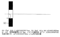
電子除去用マグネット32としては閉じた磁気回路が用いられ、その作用は図3に示す。すなわち負の荷電粒子が50eVで閉じた磁気回路で構成される5mm幅の垂直磁場(図面の表面がN極、裏面がS極:中心磁場強度は1.0×10 −2 テスラ)を通るときの軌道の計算結果の例が示されている。質量の小さな電子は磁場によって曲げられ垂直磁場を通過できないが、質量の重い負イオンは垂直磁場に大きく曲げられることもなく通過することができる。閉じた磁気回路を用いるのはこの垂直磁場の厚みを大きくしないためである。単に磁石を2個上下に配置したのでは開いた磁気回路が形成され、磁力線が空間に広がり、磁石の前後でも大きな磁場を形成する。広い空間に磁場が存在する場合、重い負イオンであってもその軌道は大きく曲げられ、質量分析器34に導くことが困難になる。
【0015】
実際の測定では、厚み3mmの2個の磁石を純鉄のドーナツ状円盤に取り付けて磁気回路を形成した。中心の磁場は1.5×10 −2 テスラである。
質量分析器34を通過するイオンのエネルギーは10eV前後が望ましいが、この例ではイオンの発散をできるだけ小さくするため20eVとした。
【0016】
ところで、図示実施例では負イオン測定用質量分析器を高周波印加電極に取り付けた例について記載してきたが、接地電位となっている壁面(或いは対向電極)に取り付けて測定するときも全く同じに実施することができる。ただその場合には、基板電位とプラズマ電位の差(基板シース電位)が接地電位となっている壁面の電位とプラズマ電位の差(壁面シース電位)よりも大きくする必要がある。従って、本発明は、当然エッチングプラズマのみならずCVDプラズマでも負イオンを 測定できる。
【0017】
【発明の効果】
以上説明してきたように、本発明によれば、高周波電力印加基板へ入射する負イオン種の分析ができるので、プラズマを形成して導入気体をプラズマ分解し、発生した原子、分子、ラジカル、イオンを利用して基板を処理するプロセスにおいて例えばエッチングプラズマ中の負イオンの種類及び量を知ることができ、エッチングプラズマについてより詳細な情報を得ることが可能となり得る。特に、半導体や電子部品加工に用いられている反応性イオンエッチングプロセスをより深く理解することができ、本発明はプロセス開発に大きく役立つ有用なものである。
【図面の簡単な説明】
【図1】 本発明の一実施例を示す概略構成図。
【図2】 図1の装置における負イオン分析のための電位の印加の仕方を示す図。
【図3】 電子除去用マグネットの作用を示す図。
【図4】 接地電位部に接続された従来のイオンエネルギー分析器及び質量分析器の一例を示す概略構成図。
【図5】 別の従来例を示す概略構成図。
【図6】 さらに別の従来例を示す概略構成図。
【符号の説明】
21: プラズマ室
22: プラズマ発生用高周波コイル
24: プラズマ発生用高周波電源
25: 基板電極
25a: 基板電極のイオン引き込み用開口
30:質量分析部
31:イオン引込電極
32:電子除去用マグネット
33:イオンエネルギー制御電極
34:質量分析器
35:イオン検出器
36:イオンエネルギー制御電源
37:質量分析用制御電源
38:電源[0001]
BACKGROUND OF THE INVENTION
The present invention uses plasma to determine the mass of negative ions in the plasma of an etching apparatus that etches a substance on a semiconductor or electronic component or other substrate, or a plasma CVD apparatus that deposits another substance on the substrate. It relates to negative ion mass spectrometry and equipment to be monitored.
[0002]
[Prior art]
For example, in an etching apparatus, a halogen-based gas is introduced into a vacuum chamber, plasma is formed by applying alternating power or high-frequency power, and the generated ions and radicals are used to etch the substrate. In this case, the plasma potential always has a positive potential with respect to the substrate and the wall surface. Therefore, positive ions generated in the plasma fly with respect to the substrate and the wall surface with this positive potential with respect to the substrate and the wall surface. To do. However, negative ions generated in the plasma are blocked by the sheath potential formed between the plasma and the substrate and the wall surface, and cannot reach the substrate and the wall surface. Therefore, positive ion measurement is easy, but negative ion measurement is difficult.
[0003]
FIGS. 4 and 5 of the accompanying drawings show a method for measuring ion energy and mass in plasma according to the prior art. FIG. 4 shows positive ions incident on a wall surface having a ground potential reported by Coburn et al. The apparatus used to measure the mass and energy distribution of (see J. Appl. Phys., 43 (1972) 4965) is shown.
In this example, since the electrode to which the mass analyzer is attached is a ground electrode, positive ions in the plasma enter the mass analyzer with the energy of the difference between the plasma potential and the ground potential.
On the other hand, FIG. 5 shows an example of a mass spectrometer with an energy analyzer attached to a substrate electrode to which high-frequency power is applied. In these cases, positive ions incident on the substrate electrode are analyzed with the energy of the difference between the plasma potential and the substrate electrode potential.
Thus, since positive ions are easily incident on the substrate electrode, measurement is easy, but measurement of negative ions in plasma is difficult and almost no reports have been made. Since the plasma potential has a positive potential and the sheath acts as a blocking potential for negative charges, it cannot be measured by the same method as the measurement of positive ions. Also, the presence of a large amount of electrons makes measurement difficult. However, many examples of negative ion measurements in the afterglow region have been reported (eg: LJ Overzet, JH Beberman and JT Verdeyen, J. App. Phys., 66 (1989) 1622, and AA Howling, JL Dorier and Ch. Hollenstein, App. Phys. Lett., 62 (1993) 1341). This is presumably because almost no sheath is formed in the afterglow region, and the electron density decreases and the negative ion density increases due to electron attachment.
In the measurement method reported by Coburn et al. In FIG. 4, since the electrode to which the mass analyzer is attached is a ground electrode, the positive ions in the plasma are expressed by the energy of the difference between the plasma potential and the ground potential. Is incident on. By this method, the energy and mass of positive ions incident on the ground potential substrate, such as plasma CVD and anodic-coupled plasma etching, can be determined, and elucidation of film formation mechanisms such as plasma CVD and etching mechanisms using radicals such as plasma etching. Very useful information is available.
The example shown in FIG. 5 is an example attached to a floating electrode to which high-frequency power is applied for the purpose of measuring positive ions of plasma used for reactive ion etching.
In reactive ion etching, an alternating electric field or a high-frequency electric field is applied to the floating potential substrate electrode, a negative self-bias is generated, a large potential difference is generated between the plasma potential and the substrate potential, and a large positive ion energy is obtained. The substrate is being etched. At this time, the substrate electrode is at a potential synthesized by the self-biased DC component and the AC component of the applied high-frequency electric field. In the example of FIG. 5, the potentials of the ion analyzer and the mass analyzer are equal to the DC component of the substrate electrode, which is a floating potential, but not exactly equal to the potential of the substrate electrode.
[0004]
FIG. 6 shows the structures of an ion energy analyzer and a mass analyzer incident on the floating electrode substrate previously proposed in Japanese Patent Application No. 8-77159. In FIG. 6, reference numeral 1 denotes a plasma generation chamber. A
An
In this structure, the analyzer and the control power source such as the
[0005]
In the case of the example of FIG. 5 where the energy analyzer is equal only to the DC component of the substrate electrode, perturbation of the high frequency component acts between the substrate electrode and the energy analyzer. The energy spectrum of ions flying in a high-frequency electric field is different depending on the time of perturbation of the high-frequency electric field, and it becomes a so-called bimodal type that is biased toward the high speed side and the low speed side. If a high-frequency potential is applied between the substrate electrode and the energy analyzer, it is considered that ions are perturbed and the spectrum shape is affected. By setting the DC potential and the high-frequency potential to the same potential, this problem can be solved and an accurate ion spectrum can be obtained.
On the other hand, in the negative ion analysis in the afterglow, since a sheath is not formed between the plasma and the analysis portion, the measurement can be performed by applying a potential for drawing a small amount of negative ions. However, the measurement of the negative ions in the plasma in which the sheath to be measured here is formed has a large sheath potential, so it is not easy to draw the negative ions and it is very difficult.
[0006]
[Problems to be solved by the invention]
Conventional ion species analysis methods in plasma target only positive ions incident on a substrate or a wall surface. Positive ions generated in the plasma fly by the difference between the plasma potential and the substrate potential or the wall potential that is normally at the ground potential, and enter the substrate or the wall surface. Since the positively charged particles generated in the plasma are only positive ions, only positive ions are incident on the measuring instrument.
On the other hand, negatively charged particles generated in plasma include electrons and negative ions. Since the plasma has a higher positive potential than the substrate and the wall surface, the negatively charged particles in the plasma are confined in the plasma. Electrons have a relatively large energy distribution, and high energy electrons can reach the substrate or wall at the moment when the sheath is minimized. However, since the energy of negative ions is small, it is impossible to get over the sheath and reach the substrate or the wall surface.
Therefore, in order to measure negative ions in the plasma, it is necessary to break the sheath potential that is the blocking potential and extract the negative ions. Moreover, even if a particle having a negative charge is pulled out by breaking the sheath, negative ions cannot be measured unless a large amount of electrons having a negative charge is removed.
Therefore, an object of the present invention is to provide a method and an apparatus that enable measurement of negative ions in plasma, which has been difficult in the past as described above.
[0007]
[Means for Solving the Problems]
In order to achieve the above object, according to the first aspect of the present invention, a gas mainly composed of reactive gas is introduced into a vacuum, and plasma is generated by alternating power, high frequency power, microwave power, etc. at low pressure. In the apparatus for processing the substrate mounted on the substrate electrode in contact with the plasma using the generated atoms, molecules, radicals, and ions by plasma decomposition of the introduced gas, an orifice is provided through the opening of the substrate electrode A negative charged particle extraction electrode is inserted to the plasma end, and the sheath formed between the plasma and the substrate electrode or the wall surface is broken and applied in a minute region by applying a potential higher than the plasma potential to the orifice. vertical magnetic field by the magnetic circuit of the integral and the S and N poles are oppositely spaced apart in a direction perpendicular to the charged particle pulled out, the negative flow direction of the charged particles drawn out of the Eliminating the internal electron negative charged particles, mass spectrometry of the negative ions in the plasma, characterized in that by passing mass spectrometry only negative ions is provided over.
[0008]
Further, according to the second invention of the present invention, a plasma generation chamber for generating plasma, a substrate electrode disposed at a position in contact with the plasma in the plasma generation chamber and having an opening through which ions in the plasma pass, and a substrate In a device having a mass analyzer for analyzing the mass of ions entering through the opening of the electrode and configured to analyze the mass of ions, a system formed between the plasma and the wall surface or the substrate electrode Negatively charged particle extraction electrode having an orifice inserted to the plasma end through the opening of the substrate electrode, while being applied with a potential higher than the plasma potential for pulling out negative charged particles in a minute region And forming a vertical magnetic field by an integrated magnetic circuit in which the S pole and the N pole are arranged opposite to each other in a direction perpendicular to the flow direction of the extracted negative charged particles. And a vertical magnetic field generating means for eliminating electrons.
[0009]
In each invention, the potential applied to the orifice is preferably set to 20 to 100 V higher than the plasma potential.
The weak vertical magnetic field applied in the direction perpendicular to the inflow direction of the negatively charged particles drawn out through the orifice is preferably 5.0 × 10 −3 to 2.0 × 10 −2 Tesla .
[0010]
[Action]
In each invention of the present invention configured as described above, since the negative charged particle extraction electrode having a minute orifice for drawing negatively charged particles can be inserted to the plasma end, the plasma can be disturbed. In addition, since only the electrons are removed by superimposing a weak vertical magnetic field by a closed magnetic circuit, only negative ions can be guided to the analyzer without greatly bending the ion trajectory, Negative ion mass spectrometry is possible.
[0011]
DETAILED DESCRIPTION OF THE INVENTION
Embodiments of the present invention will be described below based on the embodiments shown in FIGS.
【Example】
FIG. 1 shows an apparatus for measuring negative ions in plasma according to an embodiment of the present invention. In FIG. 1,
A
[0012]
The ion
In FIG. 1, 41 is a photocoupler, 42 is an optical fiber, and 43 is a measurement circuit, which are connected as shown.
[0013]
Next, the principle of negative ion measurement will be described with reference to FIGS.
FIG. 2 schematically shows the potential distribution of the device according to the invention. V1 is a voltage applied to the orifice of the
[0014]
A closed magnetic circuit is used as the
[0015]
In actual measurement, two magnets with a thickness of 3 mm were attached to a pure iron donut disk to form a magnetic circuit. The central magnetic field is 1.5 × 10 −2 Tesla .
The energy of ions passing through the
[0016]
By the way, in the illustrated embodiment, an example in which a mass spectrometer for negative ion measurement is attached to a high-frequency application electrode has been described, but the same operation is performed when attaching to a wall surface (or counter electrode) that is at ground potential. can do. However, in that case, it is necessary to make the difference between the substrate potential and the plasma potential (substrate sheath potential) larger than the difference between the wall potential and the plasma potential (wall sheath potential) that is the ground potential. Therefore, the present invention can naturally measure negative ions not only in etching plasma but also in CVD plasma.
[0017]
【The invention's effect】
As described above, according to the present invention, negative ion species incident on the high-frequency power application substrate can be analyzed, so that the introduced gas is decomposed into plasma, and the generated atoms, molecules, radicals, ions are generated. In the process of processing the substrate by using, for example, the kind and amount of negative ions in the etching plasma can be known, and more detailed information on the etching plasma can be obtained. In particular, the reactive ion etching process used in semiconductor and electronic component processing can be understood more deeply, and the present invention is useful for greatly developing processes.
[Brief description of the drawings]
FIG. 1 is a schematic configuration diagram showing an embodiment of the present invention.
FIG. 2 is a diagram showing how to apply a potential for negative ion analysis in the apparatus of FIG. 1;
FIG. 3 is a diagram showing an operation of an electron removing magnet.
FIG. 4 is a schematic configuration diagram showing an example of a conventional ion energy analyzer and mass analyzer connected to a ground potential unit.
FIG. 5 is a schematic configuration diagram showing another conventional example.
FIG. 6 is a schematic configuration diagram showing still another conventional example.
[Explanation of symbols]
21: Plasma chamber
22: High frequency coil for plasma generation
24: High frequency power supply for plasma generation
25: Substrate electrode
25a: Opening for ion drawing of substrate electrode
30: Mass spectrometer
31: Ion attracting electrode
32: Electron removal magnet
33: Ion energy control electrode
34: Mass spectrometer
35: Ion detector
36: Ion energy control power supply
37: Control power supply for mass spectrometry
38: Power supply
Claims (6)
Priority Applications (1)
| Application Number | Priority Date | Filing Date | Title |
|---|---|---|---|
| JP00017297A JP3774525B2 (en) | 1997-01-06 | 1997-01-06 | Method and apparatus for measuring negative ions in plasma |
Applications Claiming Priority (1)
| Application Number | Priority Date | Filing Date | Title |
|---|---|---|---|
| JP00017297A JP3774525B2 (en) | 1997-01-06 | 1997-01-06 | Method and apparatus for measuring negative ions in plasma |
Publications (2)
| Publication Number | Publication Date |
|---|---|
| JPH10199474A JPH10199474A (en) | 1998-07-31 |
| JP3774525B2 true JP3774525B2 (en) | 2006-05-17 |
Family
ID=11466601
Family Applications (1)
| Application Number | Title | Priority Date | Filing Date |
|---|---|---|---|
| JP00017297A Expired - Lifetime JP3774525B2 (en) | 1997-01-06 | 1997-01-06 | Method and apparatus for measuring negative ions in plasma |
Country Status (1)
| Country | Link |
|---|---|
| JP (1) | JP3774525B2 (en) |
Families Citing this family (3)
| Publication number | Priority date | Publication date | Assignee | Title |
|---|---|---|---|---|
| JP4774140B2 (en) * | 2000-01-25 | 2011-09-14 | 株式会社アルバック | Method and apparatus for analyzing energy of high-speed neutral particles incident on high-frequency power application electrode |
| JP2007194094A (en) * | 2006-01-20 | 2007-08-02 | Shimadzu Corp | Mass spectrometer |
| US11996278B2 (en) * | 2020-03-31 | 2024-05-28 | Atonarp Inc. | Plasma generating device |
-
1997
- 1997-01-06 JP JP00017297A patent/JP3774525B2/en not_active Expired - Lifetime
Also Published As
| Publication number | Publication date |
|---|---|
| JPH10199474A (en) | 1998-07-31 |
Similar Documents
| Publication | Publication Date | Title |
|---|---|---|
| Ingram | The influence of substrate topography on ion bombardment in plasma etching | |
| US7453059B2 (en) | Technique for monitoring and controlling a plasma process | |
| CN101401187B (en) | Technique for monitoring and controlling a plasma process | |
| KR101153106B1 (en) | Faraday dose and uniformity monitor for plasma based ion implantion | |
| Odom et al. | A study of electron attachment to SF6 and auto-detachment and stabilization of SF6 | |
| Verdeyen et al. | Modulated discharges: Effect on plasma parameters and deposition | |
| JP2799090B2 (en) | Ion implanter | |
| US20250323014A1 (en) | Detection systems in semiconductor metrology tools | |
| Kurihara et al. | Plasma characteristics observed through high-aspect-ratio holes in plasma | |
| JP3774525B2 (en) | Method and apparatus for measuring negative ions in plasma | |
| JP3769341B2 (en) | Method and apparatus for analyzing negative ions incident on substrate in etching plasma | |
| Overzet et al. | Negative ion extraction from pulsed discharges | |
| KR100894437B1 (en) | High Brightness Plasma Ion Beam Generator Using Local Discharge Around the Outlet by Positive Bias Electrode | |
| KR20030051751A (en) | A probe assembly for detecting an ion in a plasma generated in an ion source | |
| JP3561422B2 (en) | Atmospheric pressure ion source | |
| Dalvie et al. | Detection and modelling of electrode topography effects on particle traps | |
| JP3550457B2 (en) | Method and apparatus for analyzing energy and mass of ions incident on a floating potential substrate | |
| Jovanović et al. | Three dimensional double layers in magnetized plasmas | |
| JPH0727771A (en) | Scanning probe microscope | |
| Abraham et al. | Electrical and plasma property measurements of a deep reactive ion etching Bosch process | |
| Myers et al. | Energy and mass‐resolved detection of neutral and ion species using modulated‐pole‐bias quadrupole mass spectroscopy | |
| Mizutani et al. | Mass analysis of negative ions in etching plasma | |
| JP3096985B2 (en) | Ion source with mass separation mechanism | |
| Sanchez et al. | Extraction characteristics of ions in a magnetized sheet plasma | |
| JP4774140B2 (en) | Method and apparatus for analyzing energy of high-speed neutral particles incident on high-frequency power application electrode |
Legal Events
| Date | Code | Title | Description |
|---|---|---|---|
| A977 | Report on retrieval |
Free format text: JAPANESE INTERMEDIATE CODE: A971007 Effective date: 20041126 |
|
| A131 | Notification of reasons for refusal |
Free format text: JAPANESE INTERMEDIATE CODE: A131 Effective date: 20041207 |
|
| A521 | Written amendment |
Free format text: JAPANESE INTERMEDIATE CODE: A523 Effective date: 20050207 |
|
| A131 | Notification of reasons for refusal |
Free format text: JAPANESE INTERMEDIATE CODE: A131 Effective date: 20050726 |
|
| A521 | Written amendment |
Free format text: JAPANESE INTERMEDIATE CODE: A523 Effective date: 20050921 |
|
| TRDD | Decision of grant or rejection written | ||
| A01 | Written decision to grant a patent or to grant a registration (utility model) |
Free format text: JAPANESE INTERMEDIATE CODE: A01 Effective date: 20060124 |
|
| A61 | First payment of annual fees (during grant procedure) |
Free format text: JAPANESE INTERMEDIATE CODE: A61 Effective date: 20060220 |
|
| R150 | Certificate of patent or registration of utility model |
Free format text: JAPANESE INTERMEDIATE CODE: R150 |
|
| FPAY | Renewal fee payment (event date is renewal date of database) |
Free format text: PAYMENT UNTIL: 20120224 Year of fee payment: 6 |
|
| FPAY | Renewal fee payment (event date is renewal date of database) |
Free format text: PAYMENT UNTIL: 20130224 Year of fee payment: 7 |
|
| FPAY | Renewal fee payment (event date is renewal date of database) |
Free format text: PAYMENT UNTIL: 20130224 Year of fee payment: 7 |
|
| FPAY | Renewal fee payment (event date is renewal date of database) |
Free format text: PAYMENT UNTIL: 20140224 Year of fee payment: 8 |
|
| R250 | Receipt of annual fees |
Free format text: JAPANESE INTERMEDIATE CODE: R250 |
|
| R250 | Receipt of annual fees |
Free format text: JAPANESE INTERMEDIATE CODE: R250 |
|
| R250 | Receipt of annual fees |
Free format text: JAPANESE INTERMEDIATE CODE: R250 |
|
| EXPY | Cancellation because of completion of term |