JP3773732B2 - Liquid crystal display device and electric / electronic device using the same - Google Patents
Liquid crystal display device and electric / electronic device using the same Download PDFInfo
- Publication number
- JP3773732B2 JP3773732B2 JP37528199A JP37528199A JP3773732B2 JP 3773732 B2 JP3773732 B2 JP 3773732B2 JP 37528199 A JP37528199 A JP 37528199A JP 37528199 A JP37528199 A JP 37528199A JP 3773732 B2 JP3773732 B2 JP 3773732B2
- Authority
- JP
- Japan
- Prior art keywords
- liquid crystal
- crystal display
- display device
- driving substrate
- crystal driving
- Prior art date
- Legal status (The legal status is an assumption and is not a legal conclusion. Google has not performed a legal analysis and makes no representation as to the accuracy of the status listed.)
- Expired - Fee Related
Links
Images


Description
【0001】
【発明の属する技術分野】
この発明は不要輻射を抑制するために内部基板の構成や実装構造を改良した液晶表示装置及びこれを用いた電気・電子機器に関するものである。
【0002】
【従来の技術】
近年における液晶表示装置の画質向上の要望から、内部の液晶表示素子の高微細化が図られており、液晶表示素子を駆動させる駆動回路などの基板への実装も高密度化されている。このため、接地パターンの面積を十分に大きくとることができないために装置内外のノイズの影響を受けて安定した表示品質が得られなかったり、EMI( Electro Magnetic Interference ;電波雑音干渉)を引き起こす電磁波の不要輻射が発生する問題があった。
【0003】
このような問題を解決するものとして、例えば特開平6−82803号公報に開示された液晶表示装置がある。
図11はこの特開平6−82803号公報に開示された従来の液晶表示装置を示す断面図である。図において、4は液晶表示画面、14は液晶表示素子、15はプリント基板、16は導光体19とプリント基板15との間に配置されて、プリント基板15の不図示の接地パターンと電気的に接続する金属板、17は金属板16とプリント基板15との間に設けられた絶縁層、18は絶縁層17の4つの角に設けた切り欠き部、19は導光体である。20は液晶表示装置の各構成部を収納する金属製フレーム、21はプリント基板15に実装された電子部品、22は液晶表示素子14とプリント基板15とを電気的に接続するインタコネクタ、23は金属製フレーム20の上面に設けられた液晶表示窓である。
【0004】
概要について説明すると、金属板16及び絶縁層17は、プリント基板15或いは導光体19とほぼ同一の寸法の広い面積を有しており、これらと隣接してプリント基板15を配置し、金属板16とプリント基板15上に形成した接地パターンとを絶縁層17の切り欠き部18の箇所で電気的に接続している。これにより、安定した接地ラインが供給されて、外部から侵入するノイズや内部で発生するノイズの影響を除くことができ、安定した表示品質を得ることができる。また、EMIを引き起こすような不要な輻射電波の発生を抑制することもできる。
【0005】
また、液晶表示装置に限らず、上記のように外部から侵入するノイズや内部で発生するノイズの影響を除くことを目的とするシールド構造は様々なものがあり、例えば特開平11−17377号公報に開示されている電子回路のシールド構造がある。これは電子回路を電波から遮蔽するシールド構造に係り、特にアンテナを有する高周波回路のシールド構造に関するものである。
図12はこの特開平11−17377号公報に開示された従来の電子回路のシールド構造を示す断面図である。図において、15は導電層24を2枚の基板で挟み込んでなるプリント基板、24は導電層、25はプラスチック製の平箱状を有するシールドケース、27はプリント基板15上に実装した高周波回路ブロック、28はプリント基板15の高周波回路ブロック27を実装した面と反対側の面に実装したアンテナ、29はスルーホール31の開口部周辺に形成した接地電極層、30はスルーホール31の内壁に形成した内壁導電層、31はプリント基板15を貫通するスルーホール、32はシールドケース25の開口部周辺に設けた段差部、33はシールドケース25の内面に形成した導電性塗料膜である。
【0006】
概要について説明すると、プリント基板15は高周波回路ブロック27を実装した面が内側になるようにシールドケース25の開口部の段差部32に装着される。このとき、シールドケース25の内面に形成されている導電性塗料膜33と接地電極層29とが接触しており、プリント基板15の導電層24とシールドケース25の内面に形成した導電性塗料膜33とが内壁導電層30を介して導通している。これにより、高周波回路ブロック27は、互いに電気的に接続された導電層24、スルーホール31、スルーホール31の内壁導電層30、接地電極層29、及び導電性塗料膜33からなるシールド構造の内部に収納され、外部の電波から遮蔽され、また、内部の電波が外部に漏洩することがなくなる。
【0007】
【発明が解決しようとする課題】
従来の液晶表示装置は以上のように構成されているので、プリント基板15上に実装した電子部品が遮蔽されていないために、プリント基板15上の電子部品からの不要輻射電波を充分に抑制することができないという課題があった。
【0008】
また、金属板16がプリント基板15以外の構成部とは電気的に接続されておらず、金属板16とプリント基板15の接地パターンとの接続が弱い場合には、金属板16が逆にアンテナとして放射源として働いてしまう可能性があるという課題があった。
【0009】
さらに、プリント基板15上に実装した電子部品から発生する熱を放熱する機構がないためにプリント基板15の直下のみが高温となり、電子部品の特性を劣化させる可能性があるという課題があった。
【0010】
また、上記のような不要輻射電波を充分に抑制することができない液晶表示装置を用いた電気・電子機器が、他の電気・電子機器との間にEMIを引き起こすという課題があった。
【0011】
これに対して、上記電子回路のシールド構造を液晶表示装置に適用することも考えられた。これはシールド構造の各構成部が電気的に接続されていることから各構成部が十分に接地されており、上記のような電波の放射源となるようなことがなく、また、高周波回路ブロック27の代わりに液晶駆動用回路を実装したプリント基板を使用し、液晶駆動用回路を実装した面が内側になるようにシールドケース25の開口部の段差部32に装着することで、液晶駆動用回路を外部からの電波から遮蔽し、内部の液晶駆動用回路からの電波漏洩を抑制しようとするものである。しかしながら、このような構成では液晶駆動用回路がシールドケース25内に密封されてしまうために動作検査などを行うときに液晶駆動用回路のプリント基板15からシールドケース25を取り外す作業が必要で手間がかかってしまう。また、プリント基板15の液晶駆動用回路が実装されていない面に液晶パネルを設けることとなるために、液晶パネル側から液晶駆動用回路を遮蔽することができず、不十分な遮蔽構造をとらざるを得なかった。
【0012】
この発明は上記のような課題を解決するためになされたもので、液晶表示装置からの不要な輻射電波の発生を抑制し、液晶駆動用回路から発生する熱を放熱することができる液晶表示装置及びこれを用いた電気・電子機器を得ることを目的とするものである。
【0013】
【課題を解決するための手段】
この発明に係る液晶表示装置は、液晶駆動用基板が一方の面に部品実装面、他方の面に接地面を有し、この接地面と導電性反射板とを電気的に接続するとともに、部品実装面側から導電性反射板に支持固定するものである。
【0014】
この発明に係る液晶表示装置は、液晶駆動用基板及び/若しくは導電性反射板に設けられ、液晶駆動用基板を導電性反射板に支持固定する係合部を備え、この係合部を介して接地面と導電性反射板とを電気的に接続するものである。
【0015】
この発明に係る液晶表示装置は、係合ネジ孔及び係合ネジ部から係合部が構成されるものである。
【0016】
この発明に係る液晶表示装置は、導電性反射板に設けられ、液晶駆動用基板を係合固定する爪部から係合部が構成されるものである。
【0017】
この発明に係る液晶表示装置は、導電性反射板に設けられ、液晶駆動用基板の取付位置を決定する取り付けガイド部を備えるものである。
【0018】
この発明に係る液晶表示装置は、導電性反射板に設けられ、液晶駆動用基板に実装した部品から発生する熱を放熱する放熱手段を備えるものである。
【0019】
この発明に係る電気・電子機器は、請求項1から請求項6のうちのいずれか1項記載の液晶表示装置を備えるものである。
【0020】
【発明の実施の形態】
以下、この発明の実施の一形態を説明する。
実施の形態1.
液晶表示装置を大きく分けると、透過型液晶表示装置と反射型液晶表示装置とがある。簡単に説明すると、反射型液晶表示装置は、液晶表示部や液晶セルなどからなる液晶パネルと、この液晶パネルの背面に設置した反射板とを有し、液晶パネルの液晶表示面側から偏光板などを介して入射した光を、上記反射板にて反射して液晶表示面側へ戻し、この反射光を液晶表示部の照明とするものである。また、透過型液晶表示装置は、液晶表示部、液晶セル、及び背面照明装置(バックライト)などからなる液晶パネルと、背面照明装置からの光を液晶表示部側に反射する反射板とを有し、背面照明装置からの光を反射板にて反射して、この反射光を液晶表示部の照明とするものである。本願発明の液晶表示装置は上記透過型、反射型のどちらにも適用することができ、上記反射板を導電性の材料からなる導電性反射板とする。以下に示す実施の形態では、説明の簡単のために本願発明を透過型液晶表示装置に適用した場合について述べる。
【0021】
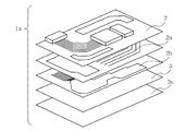
図1はこの発明の実施の形態1による液晶表示装置の液晶駆動用基板の構成を示す分解斜視図、図2は実施の形態1による液晶駆動用基板の他の構成を示す分解斜視図、図3は実施の形態1による液晶表示装置における液晶駆動用基板の液晶パネルへの実装構造を示す斜視図である。図において、1は液晶駆動用基板で、一方の面に液晶表示素子を駆動させる液晶駆動用回路などを実装する部品実装面2とし、他方の面の全面に金属薄膜層を形成して接地面3としており、図示の例では内層に設けた信号線層の信号線2a及び電源層の電源2bを備えた多層基板から構成されている。1aは他の例の液晶駆動用基板で、一方の面に液晶表示素子を駆動させる液晶駆動用回路などを実装する部品実装面2とし、他方の面は電子部品を実装せずに、配線パターンが露出した未実装面3aとする。この未実装面3aは内層に隣接して接地面3が設けられ、この接地面3と未実装面3aの配線パターンとを電気的に接続することで接地面を形成している。4は液晶表示部、5はバックライト、6は金属製反射板(導電性反射板)で、バックライト5からの光を反射して液晶表示部4に照明光を供給する。7は液晶表示部4、バックライト5、及び金属製反射板6からなる液晶パネル、8は液晶パネル7及び液晶駆動用基板1からなる本願発明の液晶表示装置である。
【0022】
次に概要について説明する。
液晶駆動用基板1,1aは、一方を部品実装面2、他方を全面の接地面3若しくは接地パターンを設けた未実装面3aとしており、この液晶駆動用基板1,1aは金属製反射板6にて支持固定される。このとき、図3に示すように液晶駆動用基板1,1aの部品実装面2を金属製反射板6に向けて支持固定し、同時に接地面3や未実装面3aと金属製反射板6とを電気的に接続する。このようにすることで、不要輻射電波を発生する主要因である液晶駆動用回路を構成する電子部品、信号線2a、及び電源2bが、金属製反射板6と接地面3又は未実装面3aとの間に挟まれ、さらに、金属製反射板6と接地面3又は未実装面3aとの電気的接続により、外部の電波が遮蔽され、液晶駆動用基板1,1aからの不要輻射電波を阻止する遮蔽構造を構成する。
【0023】
これにより、液晶駆動用基板1,1aから発生した電磁波が、例えば液晶表示装置8の筐体などの液晶駆動用基板1,1a外部の構成部と干渉することを抑制することができる。また、不要輻射電波を抑制するための特別な遮蔽構造を設ける必要がないので、部品点数を削減でき、製造の容易化及び低コスト化を図ることができる。
【0024】
なお、金属製反射板6と液晶駆動用基板1,1aの接地面3、未実装面3aとの電気的接続は、接地面3又は未実装面3aと電気的に接続する箇所を液晶駆動用基板1,1aの部品実装面2上に設けた場合は、この接続箇所と金属製反射板6とを電気的に接続してもよい。
【0025】
以上のように、この実施の形態1によれば、液晶駆動用基板1,1aが一方の面に部品実装面2、他方の面に接地面3若しくは接地パターンを有する未実装面3aを有し、接地面3若しくは接地パターンを有する未実装面3aと金属製反射板6とを電気的に接続するとともに、部品実装面2側から金属製反射板6に支持固定するので、液晶表示装置8の主たるノイズ源である液晶駆動用回路を構成する電子部品、信号線2a、及び電源2bなどを金属製反射板6及び接地面3若しくは未実装面3aにて遮蔽することができることから、液晶表示装置8から発生する不要輻射電波を抑制することができる。
【0026】
また、液晶駆動用基板1,1aから発生した電磁波が、例えば液晶表示装置8の筐体などの液晶駆動用基板1,1a外部の構成部と干渉することを抑制することができる。
【0027】
さらに、不要輻射電波を抑制するための特別な遮蔽構造やEMI対策用の新たな部材を設ける必要がないので、部品点数を削減でき、製造の容易化及び低コスト化を図ることができる。
【0028】
実施の形態2.
この実施の形態2は液晶駆動用基板を導電性反射板に支持固定し、同時に接地面と導電性反射板とを電気的に接続する係合部を備えるものである。
【0029】
図4はこの発明の実施の形態2による液晶表示装置における液晶駆動用基板の実装構造を示す斜視図である。図において、9aは液晶駆動用基板1を金属製反射板6に支持固定する固定用ネジ(係合ネジ部、係合部)、9bは金属製反射板6に設けられ、固定用ネジ9aと螺合するネジ孔(係合ネジ孔、係合部)である。なお、図3と同一構成要素には同一符号を付して重複する説明を省略する。
【0030】
次に概要を説明する。
固定用ネジ9aは導電性材料から形成し、金属製反射板6に設けた貫通孔を通して、金属製反射板6のネジ孔9bと螺合させて液晶駆動用基板1を金属製反射板6に支持固定する。このとき、同時に固定用ネジ9aを介して接地面3と金属製反射板6とが電気的に接続される。
【0031】
図5はこの発明の実施の形態2による液晶表示装置における液晶駆動用基板の他の実装構造を示す斜視図である。図において、10は金属製反射板6に設けられ、液晶駆動用基板1を金属製反射板6に支持固定する固定用爪(爪部、係合部)である。なお、図3と同一構成要素には同一符号を付して重複する説明を省略する。
【0032】
次に概要を説明する。
固定用爪10は導電性材料から形成し、液晶駆動用基板1の側面及び接地面3を圧接するように鉤状を有している。液晶駆動用基板1は固定用爪10の上方から導入して支持固定する。このとき、容易に取り付けできるように固定用爪10には上方から下方にスロープを設けて固定用爪10の摩擦力を低減させており、液晶駆動用基板1は上記スロープ上を滑るように導入されて固定用爪10と嵌合する。また、接地面3と金属製反射板6との電気的接続は、固定用爪10の接地面3との圧接面において行われる。
【0033】
また、上記実施の形態2では、液晶駆動用基板1を金属製反射板6に支持固定する係合部として、固定用ネジ9a、ネジ孔9b、及び固定用爪10を設けた例について示したが、本願発明はこれに限らず、液晶駆動用基板1を金属製反射板6に確実に固定し、且つ、接地面3と金属製反射板6とを電気的に接続することのできる構造であればよい。
【0034】
さらに、金属製反射板6と液晶駆動用基板1の接地面3との電気的接続は、接地面3と電気的に接続する箇所を液晶駆動用基板1の部品実装面2上に設けた場合は、この接続箇所と金属製反射板6との電気的接続を固定用爪10で行うようにしてもよい。
【0035】
以上のように、この実施の形態2では、液晶駆動用基板1及び/若しくは金属製反射板6に設けられ、液晶駆動用基板1を金属製反射板6に支持固定する係合部(固定用ネジ9a、ネジ孔9b、固定用爪10)を備え、この係合部を介して接地面3と金属製反射板6とを電気的に接続するので、液晶駆動用基板1の金属製反射板6への支持固定と、接地面3と金属製反射板6との電気的接続とを確実に行うことができ、より確実に電波を遮蔽する液晶表示装置を提供することができる。
【0036】
また、この実施の形態2によれば、固定用ネジ9a及びネジ孔9bから係合部が構成されるので、上記と同様の効果を奏するとともに、金属製反射板6と接地面3とが接触不良を起こして、金属製反射板6が逆にアンテナとして放射源となることを防止することができる。
【0037】
さらに、この実施の形態2によれば、金属製反射板6に設けられ、液晶駆動用基板1を係合固定する固定用爪10から係合部が構成されるので、液晶駆動用基板1の金属製反射板6への取り付け作業を容易に、且つ、確実に行うことができ、より確実に不要輻射電波を抑制する液晶表示装置を提供することができる。
【0038】
また、液晶駆動用基板1の金属製反射板6からの取り外し作業も容易に行うことができるので、液晶駆動用基板1の交換や、液晶駆動用回路の動作検査などを容易に行うことができる。
【0039】
さらに、ネジ止めや接着剤などを使用しないことから、部品点数を削減することができ、安価に液晶表示装置を提供することができる。
【0040】
なお、上記実施の形態2で挙げた固定用ネジ9a、ネジ孔9b、及び固定用爪10を併用するようにしてもよい。これにより、液晶駆動用基板1の金属製反射板6への支持固定及び接地面3と金属製反射板6との電気的接続に対する信頼性をさらに向上させることができる。
【0041】
実施の形態3.
この実施の形態3は液晶駆動用基板を導電性反射板に取り付ける際にその取付位置を決定する取り付けガイド部を導電性反射板に設けたものである。
【0042】
図6はこの発明の実施の形態3による液晶表示装置における液晶駆動用基板の液晶パネルへの実装構造を示す斜視図である。図において、11は液晶駆動用基板1の金属製反射板6への取付位置の決定を行う基板取り付けガイド(取り付けガイド部)である。なお、図3と同一構成要素には同一符号を付して重複する説明を省略する。
【0043】
次に概要を説明する。
基板取り付けガイド11は、例えば図6に示すように液晶駆動用基板1の四辺に沿う位置に配置する。液晶駆動用基板1は基板取り付けガイド11によって囲まれた領域内に部品実装面2がはめ込まれるように金属製反射板6に固定される。これにより、液晶駆動用基板1の取付位置を容易に決定することができる。
【0044】
また、基板取り付けガイド11は、図6に示したもの以外に、液晶駆動用基板1の四隅に沿うように設けるか若しくは、液晶駆動用基板1の取付位置が最低限決定することができるように、液晶駆動用基板1の四辺又は四隅の一部に沿うように設けてもよい。
【0045】
さらに、基板取り付けガイド11を、液晶駆動用基板1の外周に沿った位置に設けて、液晶駆動用基板1を金属製反射板6に取り付けた際に、基板取り付けガイド11が液晶駆動用基板1を囲むようにすることで、液晶駆動用基板1を接地面3、基板取り付けガイド11、及び金属製反射板6からなる密封空間を有する遮蔽構造を構成することができる。このようにすることで、基板取り付けガイド11による上記効果を奏するとともに、より確実に液晶表示装置8から発生する不要輻射電波を遮蔽することができる。
【0046】
図7は図6における液晶駆動用基板1の金属製反射板6への支持固定を上記実施の形態2の固定用ネジ9a及びネジ孔9bにて行う構成を示す斜視図で、図8は図6における液晶駆動用基板1の金属製反射板6への支持固定を上記実施の形態2の固定用爪10にて行う構成を示す斜視図である。なお、図4及び図5と同一構成要素には同一符号を付して重複する説明を省略する。
【0047】
次に概要を説明する。
基板取り付けガイド11は、例えば図7若しくは図8に示すように液晶駆動用基板1の四辺に沿う位置に配置する。液晶駆動用基板1は基板取り付けガイド11によって囲まれた領域内に部品実装面2がはめ込まれるように金属製反射板6に設置する。このとき、図7の例では、液晶駆動用基板1の金属製反射板6への支持固定を固定用ネジ9a及びネジ孔9bにて行い、これら固定用ネジ9a及びネジ孔9bを介して接地面3と金属製反射板6とを電気的に接続する。図8の例では、液晶駆動用基板1の金属製反射板6への支持固定を固定用爪10にて行い、固定用爪10を介して接地面3と金属製反射板6とを電気的に接続する。
【0048】
上記のように基板取り付けガイド11と、上記実施の形態2で示した固定用ネジ9a、ネジ孔9b、及び固定用爪10とを組み合わせることで、液晶駆動用基板1をより容易に且つ迅速に金属製反射板6に取り付けることができる。
【0049】
以上のように、この実施の形態3によれば、金属製反射板6に設けられ、液晶駆動用基板1の取付位置を決定する基板取り付けガイド11を備えるので、液晶駆動用基板1の取付位置を容易に決定することができる。
【0050】
なお、金属製反射板6と液晶駆動用基板1の接地面3との電気的接続は、接地面3と電気的に接続する箇所を液晶駆動用基板1の部品実装面2上に設けた場合は、この接続箇所と基板取り付けガイド11とを電気的に接続してもよい。
【0051】
実施の形態4.
この実施の形態4は液晶駆動用基板に実装した部品から発生する熱を放熱する放熱手段を導電性反射板に設けたものである。
【0052】
図9はこの発明の実施の形態4による液晶表示装置における液晶駆動用基板の液晶パネルへの実装構造を示す斜視図である。図において、6aは液晶駆動用基板1に実装した部品から発生する熱を放熱する放熱機構12を設けた金属製反射板(導電性反射板)、12は金属製反射板6aに設けられ、液晶駆動用基板1に実装した部品から発生する熱が、液晶駆動用基板1に集中しないように放熱する放熱機構(放熱手段)である。なお、図3と同一構成要素には同一符号を付して重複する説明を省略する。
【0053】
次に概要を説明する。
放射機構12は、例えば金属製反射板6aの表面(液晶駆動用基板1を支持固定したときに、液晶駆動用基板1の部品実装面2と対向する面)に多数の襞部を形成した構成とする。これらの襞部によって金属製反射板6aの表面積が広がり放熱機能を持たせることができる。また、液晶駆動用基板1は上記実施の形態1と同様に部品実装面2側から金属製反射板6aに取り付けられ、上記実施の形態2で示したような係合部によって固定される。これにより、液晶駆動用基板1に実装した部品から発生する熱は、放熱機構12を介して液晶表示装置8の外部に放熱される。
【0054】
以上のように、この実施の形態4によれば、金属製反射板6aに設けられ、液晶駆動用基板1に実装した部品から発生する熱を放熱する放熱機構12を備えるので、液晶駆動用基板1に実装した部品から発生する熱による液晶表示装置8の動作の不安定化を抑えることができる。
【0055】
なお、上記実施の形態4では、放熱機構12として金属製反射板6aの表面に多数の襞部を設けたものについて示したが、本願発明はこれに限らず、放熱機構12は液晶駆動用基板1に実装した部品から発生する熱を効率よく放熱し、液晶駆動用基板1の金属製反射板6aへの取り付けに支障を来さない構造であればよい。
【0056】
また、上記放熱機構12を設けた金属製反射板6aを、上記実施の形態1から実施の形態3の構成に適用しても上記と同様の効果を奏する。
【0057】
実施の形態5.
この実施の形態5は上記実施の形態1から実施の形態4で示した液晶表示装置を具備した電気・電子機器に関するものである。
【0058】
図10はこの発明の実施の形態5による電気・電子機器を示す斜視図である。図において、13は本願発明の液晶表示装置8を具備した電気・電子機器であり、例として液晶モニタを示している。
【0059】
次に概要を説明する。
本願発明の液晶表示装置8を具備することにより、特に不要輻射電波を抑制することができるため、電気・電子機器13が他の電気・電子機器との間のEMIを抑制することができる。このようなEMIには各種の法規制が存在し、家電、情報機器、医療機器、産業機器などの全ての電気・電子機器からの不要輻射電波に由来する妨害波の強度の許容値が規定されている。そこで、本願発明の液晶表示装置8を具備することで、上記EMIの各種法規制に適合する電気・電子機器を容易に提供することができる。
【0060】
以上のように、この実施の形態5によれば、本願発明の液晶表示装置8を電気・電子機器13が備えるので、他の電気・電子機器との間のEMIを抑制することができる。これにより、EMIの各種法規制に早期に適合させることができ、ひいては本願発明の液晶表示装置8を具備した電気・電子機器13の市場参入を早期化させることができる。
【0061】
また、本願発明の液晶表示装置8を具備することで、電気・電子機器13の製品設計後にEMI対策のための特別な部材や遮蔽構造を設ける必要がないので、EMI対策にかかるコストを削減することができる。
【0062】
【発明の効果】
この発明の液晶表示装置によれば、液晶駆動用基板が一方の面に部品実装面、他方の面に接地面を有し、この接地面と導電性反射板とを電気的に接続するとともに、部品実装面側から導電性反射板に支持固定するので、液晶表示装置の主たるノイズ源である液晶駆動用回路を構成する電子部品から発生する電波を遮蔽することができることから、液晶表示装置からの不要輻射電波を抑制することができる効果がある。
【0063】
また、液晶駆動用基板から発生した電磁波が、液晶駆動用基板外部の構成部と干渉することを抑制することができる効果がある。
【0064】
さらに、不要輻射電波を抑制するための特別な遮蔽構造やEMI対策用の新たな部材を設ける必要がないので、部品点数を削減でき、製造の容易化及び低コスト化することができる効果がある。
【0065】
この発明の液晶表示装置によれば、液晶駆動用基板及び/若しくは導電性反射板に設けられ、液晶駆動用基板を導電性反射板に支持固定する係合部を備え、この係合部を介して接地面と導電性反射板とを電気的に接続するので、液晶駆動用基板の導電性反射板への支持固定と、接地面と導電性反射板との電気的接続とを確実に行うことができ、より確実に不要輻射電波を抑制する液晶表示装置を提供することができる効果がある。
【0066】
この発明の液晶表示装置によれば、係合ネジ孔及び係合ネジ部から係合部が構成されるので、上記段落0065と同様の効果を奏するとともに、導電性反射板と接地面とが接触不良を起こして、導電性反射板が逆にアンテナとして放射源となることを防止することができる。
【0067】
この発明の液晶表示装置によれば、導電性反射板に設けられ、液晶駆動用基板を係合固定する爪部から係合部が構成されるので、液晶駆動用基板の導電性反射板への取り付け作業を容易に、且つ、確実に行うことができ、より確実に不要輻射電波を抑制する液晶表示装置を提供することができる効果がある。
【0068】
また、液晶駆動用基板の導電性反射板からの取り外し作業も容易に行うことができるので、液晶駆動用基板の交換や、液晶駆動用回路の動作検査などを容易に行うことができる効果がある。
【0069】
さらに、ネジ止めや接着剤などを使用しないことから、部品点数を削減することができ、安価に液晶表示装置を提供することができる効果がある。
【0070】
この発明の液晶表示装置によれば、導電性反射板に設けられ、液晶駆動用基板の取付位置を決定する取り付けガイド部を備えるので、液晶駆動用基板1の取付位置を容易に決定することができる効果がある。
【0071】
この発明の液晶表示装置によれば、導電性反射板に設けられ、液晶駆動用回路から発生する熱を放熱する放熱手段を備えるので、液晶駆動用基板に実装した部品から発生する熱による液晶表示装置の動作の不安定化を抑えることができる効果がある。
【0072】
この発明の電気・電子機器によれば、請求項1から請求項6のうちのいずれか1項記載の液晶表示装置を備えるので、他の電気・電子機器との間のEMIを抑制することができる効果がある。これにより、EMIの各種法規制に早期に適合させることができ、ひいては電気・電子機器の市場参入を早期化することができる。
【0073】
また、電気・電子機器の製品設計後にEMI対策のための部材や遮蔽構造を新たに設ける必要がないので、EMI対策にかかるコストを削減することができる効果がある。
【図面の簡単な説明】
【図1】 この発明の実施の形態1による液晶表示装置の液晶駆動用基板の構成を示す分解斜視図である。
【図2】 実施の形態1による液晶駆動用基板の他の構成を示す分解斜視図である。
【図3】 実施の形態1による液晶表示装置における液晶駆動用基板の液晶パネルへの実装構造を示す斜視図である。
【図4】 この発明の実施の形態2による液晶表示装置における液晶駆動用基板の実装構造を示す斜視図である。
【図5】 この発明の実施の形態2による液晶表示装置における液晶駆動用基板の他の実装構造を示す斜視図である。
【図6】 この発明の実施の形態3による液晶表示装置における液晶駆動用基板の液晶パネルへの実装構造を示す斜視図である。
【図7】 図6における液晶駆動用基板1の金属製反射板6への支持固定を上記実施の形態2の固定用ネジ9a及びネジ孔9bにて行う構成を示す斜視図である。
【図8】 図6における液晶駆動用基板1の金属製反射板6への支持固定を上記実施の形態2の固定用爪10にて行う構成を示す斜視図である。
【図9】 この発明の実施の形態4による液晶表示装置における液晶駆動用基板の液晶パネルへの実装構造を示す斜視図である。
【図10】 この発明の実施の形態5による電気・電子機器を示す斜視図である。
【図11】 従来の液晶表示装置を示す断面図である。
【図12】 従来の電子回路のシールド構造を示す断面図である。
【符号の説明】
1,1a 液晶駆動用基板、2 部品実装面、2a 信号線、2b 電源、3接地面、3a 未実装面(接地面)、4 液晶表示部、5 バックライト、6,6a 金属製反射板(導電性反射板)、7 液晶パネル、8 液晶表示装置、9a 固定用ネジ(係合ネジ部、係合部)、9b ネジ孔(係合ネジ孔、係合部)、10 固定用爪(爪部、係合部)、11 基板取り付けガイド(取り付けガイド部)、12 放熱機構(放熱手段)、13 電気・電子機器。[0001]
BACKGROUND OF THE INVENTION
The present invention relates to a liquid crystal display device in which the structure and mounting structure of an internal substrate are improved in order to suppress unnecessary radiation, and an electric / electronic device using the same.
[0002]
[Prior art]
In recent years, due to the demand for improving the image quality of liquid crystal display devices, the internal liquid crystal display elements have been highly miniaturized, and the mounting on a substrate such as a drive circuit for driving the liquid crystal display elements has also been increased in density. For this reason, since the area of the ground pattern cannot be made sufficiently large, stable display quality cannot be obtained due to the influence of noise inside and outside the apparatus, or electromagnetic waves that cause EMI (Electro Magnetic Interference). There was a problem that unnecessary radiation was generated.
[0003]
As a solution to such a problem, there is, for example, a liquid crystal display device disclosed in JP-A-6-82803.
FIG. 11 is a cross-sectional view showing a conventional liquid crystal display device disclosed in Japanese Patent Laid-Open No. 6-82803. In the figure, 4 is a liquid crystal display screen, 14 is a liquid crystal display element, 15 is a printed circuit board, 16 is disposed between the
[0004]
The outline will be described. The
[0005]
In addition to the liquid crystal display device, there are various shield structures aimed at eliminating the influence of noise entering from the outside and noise generated inside as described above. For example, Japanese Patent Application Laid-Open No. 11-17377 There is a shield structure of an electronic circuit disclosed in the above. This relates to a shield structure that shields an electronic circuit from radio waves, and particularly to a shield structure of a high-frequency circuit having an antenna.
FIG. 12 is a cross-sectional view showing a conventional shield structure for an electronic circuit disclosed in Japanese Patent Application Laid-Open No. 11-17377. In the figure, 15 is a printed circuit board in which a
[0006]
The outline will be described. The printed
[0007]
[Problems to be solved by the invention]
Since the conventional liquid crystal display device is configured as described above, the electronic components mounted on the printed
[0008]
In addition, when the
[0009]
Furthermore, since there is no mechanism for dissipating heat generated from the electronic component mounted on the printed
[0010]
In addition, there is a problem that an electric / electronic device using a liquid crystal display device that cannot sufficiently suppress unnecessary radiated radio waves as described above causes EMI with other electric / electronic devices.
[0011]
On the other hand, it has been considered to apply the shield structure of the electronic circuit to a liquid crystal display device. This is because each component of the shield structure is electrically connected, so that each component is sufficiently grounded and does not become a radio wave radiation source as described above. 27 is used instead of the printed circuit board on which the liquid crystal driving circuit is mounted, and is mounted on the
[0012]
The present invention has been made to solve the above-described problems, and can suppress generation of unnecessary radiated radio waves from a liquid crystal display device and dissipate heat generated from a liquid crystal driving circuit. And it aims at obtaining the electric / electronic device using this.
[0013]
[Means for Solving the Problems]
In the liquid crystal display device according to the present invention, the liquid crystal driving substrate has a component mounting surface on one surface and a ground surface on the other surface, and electrically connects the ground surface and the conductive reflector. It is supported and fixed to the conductive reflector from the mounting surface side.
[0014]
The liquid crystal display device according to the present invention includes an engaging portion that is provided on the liquid crystal driving substrate and / or the conductive reflecting plate and supports and fixes the liquid crystal driving substrate to the conductive reflecting plate. The ground plane and the conductive reflector are electrically connected.
[0015]
In the liquid crystal display device according to the present invention, the engaging portion is composed of the engaging screw hole and the engaging screw portion.
[0016]
In the liquid crystal display device according to the present invention, the engaging portion is configured by a claw portion that is provided on the conductive reflecting plate and engages and fixes the liquid crystal driving substrate.
[0017]
The liquid crystal display device according to the present invention includes an attachment guide portion that is provided on the conductive reflector and determines the attachment position of the liquid crystal driving substrate.
[0018]
The liquid crystal display device according to the present invention is provided with a heat radiating means for radiating heat generated from components mounted on a liquid crystal driving substrate, which is provided on a conductive reflector.
[0019]
An electric / electronic device according to the present invention includes the liquid crystal display device according to any one of claims 1 to 6.
[0020]
DETAILED DESCRIPTION OF THE INVENTION
An embodiment of the present invention will be described below.
Embodiment 1 FIG.
The liquid crystal display device is roughly classified into a transmissive liquid crystal display device and a reflective liquid crystal display device. Briefly, the reflective liquid crystal display device includes a liquid crystal panel composed of a liquid crystal display unit, a liquid crystal cell, and the like, and a reflective plate installed on the back of the liquid crystal panel, and a polarizing plate from the liquid crystal display surface side of the liquid crystal panel. The light incident through the light is reflected by the reflection plate and returned to the liquid crystal display surface side, and this reflected light is used as illumination of the liquid crystal display unit. In addition, the transmissive liquid crystal display device includes a liquid crystal panel including a liquid crystal display unit, a liquid crystal cell, and a backlight device (backlight), and a reflector that reflects light from the backlight device to the liquid crystal display unit side. And the light from a back surface illuminating device is reflected in a reflecting plate, and this reflected light is used as illumination of a liquid crystal display part. The liquid crystal display device of the present invention can be applied to both the transmission type and the reflection type, and the reflection plate is a conductive reflection plate made of a conductive material. In the following embodiments, the case where the present invention is applied to a transmissive liquid crystal display device will be described for the sake of simplicity.
[0021]
1 is an exploded perspective view showing a configuration of a liquid crystal driving substrate of a liquid crystal display device according to Embodiment 1 of the present invention, and FIG. 2 is an exploded perspective view showing another configuration of the liquid crystal driving substrate according to Embodiment 1. 3 is a perspective view showing a mounting structure of a liquid crystal driving substrate on a liquid crystal panel in the liquid crystal display device according to Embodiment 1. FIG. In the figure, reference numeral 1 denotes a liquid crystal driving substrate, which is a
[0022]
Next, an outline will be described.
One of the liquid crystal driving substrates 1 and 1a is a
[0023]
Thereby, it is possible to suppress electromagnetic waves generated from the liquid crystal driving substrates 1 and 1a from interfering with components outside the liquid crystal driving substrates 1 and 1a such as a casing of the liquid
[0024]
In addition, the electrical connection between the
[0025]
As described above, according to the first embodiment, the liquid crystal driving substrates 1 and 1a have the
[0026]
Further, it is possible to suppress the electromagnetic waves generated from the liquid crystal driving substrates 1 and 1a from interfering with components outside the liquid crystal driving substrates 1 and 1a such as a casing of the liquid
[0027]
Furthermore, since it is not necessary to provide a special shielding structure for suppressing unnecessary radiated radio waves or a new member for EMI countermeasure, the number of parts can be reduced, and manufacturing can be facilitated and cost can be reduced.
[0028]
In the second embodiment, a liquid crystal driving substrate is supported and fixed to a conductive reflecting plate, and at the same time, an engaging portion for electrically connecting the ground plane and the conductive reflecting plate is provided.
[0029]
4 is a perspective view showing a mounting structure of a liquid crystal driving substrate in a liquid crystal display device according to
[0030]
Next, an outline will be described.
The fixing
[0031]
FIG. 5 is a perspective view showing another mounting structure of the liquid crystal driving substrate in the liquid crystal display device according to
[0032]
Next, an outline will be described.
The fixing
[0033]
In the second embodiment, the example in which the fixing
[0034]
Further, the electrical connection between the
[0035]
As described above, in the second embodiment, the engagement portion (fixing member) is provided on the liquid crystal driving substrate 1 and / or the
[0036]
Further, according to the second embodiment, since the engaging portion is constituted by the fixing
[0037]
Further, according to the second embodiment, the engaging portion is formed by the fixing
[0038]
In addition, since the liquid crystal driving substrate 1 can be easily detached from the
[0039]
Furthermore, since no screwing or adhesive is used, the number of components can be reduced, and a liquid crystal display device can be provided at a low cost.
[0040]
Note that the fixing
[0041]
In the third embodiment, when the liquid crystal driving substrate is attached to the conductive reflector, an attachment guide portion for determining the attachment position is provided on the conductive reflector.
[0042]
6 is a perspective view showing a mounting structure of a liquid crystal driving substrate on a liquid crystal panel in a liquid crystal display device according to
[0043]
Next, an outline will be described.
For example, as shown in FIG. 6, the
[0044]
Further, the
[0045]
Furthermore, when the
[0046]
FIG. 7 is a perspective view showing a configuration in which the liquid crystal driving substrate 1 in FIG. 6 is supported and fixed to the
[0047]
Next, an outline will be described.
The
[0048]
By combining the
[0049]
As described above, according to the third embodiment, since the
[0050]
The electrical connection between the
[0051]
In the fourth embodiment, a heat radiating means for radiating heat generated from components mounted on a liquid crystal driving substrate is provided on a conductive reflector.
[0052]
FIG. 9 is a perspective view showing a mounting structure of a liquid crystal driving substrate on a liquid crystal panel in a liquid crystal display device according to
[0053]
Next, an outline will be described.
The
[0054]
As described above, according to the fourth embodiment, the liquid crystal driving substrate is provided with the
[0055]
In the fourth embodiment, the
[0056]
Moreover, even if the
[0057]
The fifth embodiment relates to an electric / electronic apparatus provided with the liquid crystal display device shown in the first to fourth embodiments.
[0058]
10 is a perspective view showing an electric / electronic device according to
[0059]
Next, an outline will be described.
By including the liquid
[0060]
As described above, according to the fifth embodiment, since the electric /
[0061]
In addition, by providing the liquid
[0062]
【The invention's effect】
According to the liquid crystal display device of the present invention, the liquid crystal driving substrate has a component mounting surface on one surface and a ground surface on the other surface, and electrically connects the ground surface and the conductive reflector, Since it is supported and fixed to the conductive reflector from the component mounting surface side, radio waves generated from the electronic components constituting the liquid crystal driving circuit, which is the main noise source of the liquid crystal display device, can be shielded. There is an effect of suppressing unnecessary radiated radio waves.
[0063]
Further, there is an effect that electromagnetic waves generated from the liquid crystal driving substrate can be prevented from interfering with components outside the liquid crystal driving substrate.
[0064]
Furthermore, since it is not necessary to provide a special shielding structure for suppressing unnecessary radiated radio waves or a new member for EMI countermeasures, it is possible to reduce the number of parts, and to facilitate manufacturing and reduce costs. .
[0065]
According to the liquid crystal display device of the present invention, the liquid crystal display device includes the engaging portion that is provided on the liquid crystal driving substrate and / or the conductive reflecting plate and supports and fixes the liquid crystal driving substrate to the conductive reflecting plate. Since the ground plane and the conductive reflector are electrically connected to each other, the support and fixing of the liquid crystal driving substrate to the conductive reflector and the electrical connection between the ground plane and the conductive reflector must be ensured. Thus, there is an effect that it is possible to provide a liquid crystal display device that more reliably suppresses unnecessary radiated radio waves.
[0066]
According to the liquid crystal display device of the present invention, since the engaging portion is constituted by the engaging screw hole and the engaging screw portion, the same effect as in the above paragraph 0065 is achieved, and the conductive reflector and the ground plane are in contact with each other. It is possible to prevent the conductive reflector from becoming a radiation source as an antenna.
[0067]
According to the liquid crystal display device of the present invention, since the engaging portion is formed by the claw portion that is provided on the conductive reflecting plate and engages and fixes the liquid crystal driving substrate, the liquid crystal driving substrate is connected to the conductive reflecting plate. There is an effect that it is possible to provide a liquid crystal display device that can easily and reliably perform the attaching operation and more reliably suppress unnecessary radiated radio waves.
[0068]
In addition, since the liquid crystal driving substrate can be easily detached from the conductive reflector, the liquid crystal driving substrate can be easily replaced and the liquid crystal driving circuit can be inspected. .
[0069]
Furthermore, since no screwing or adhesive is used, the number of parts can be reduced, and there is an effect that a liquid crystal display device can be provided at low cost.
[0070]
According to the liquid crystal display device of the present invention, since the mounting guide portion is provided on the conductive reflector and determines the mounting position of the liquid crystal driving substrate, the mounting position of the liquid crystal driving substrate 1 can be easily determined. There is an effect that can be done.
[0071]
According to the liquid crystal display device of the present invention, the liquid crystal display device is provided with the heat radiating means for radiating the heat generated from the liquid crystal driving circuit, provided on the conductive reflecting plate. There is an effect that the destabilization of the operation of the apparatus can be suppressed.
[0072]
According to the electric / electronic device of the present invention, since the liquid crystal display device according to any one of claims 1 to 6 is provided, it is possible to suppress EMI with other electric / electronic devices. There is an effect that can be done. As a result, it is possible to quickly conform to various EMI laws and regulations, and it is possible to accelerate the market entry of electrical / electronic devices.
[0073]
In addition, since it is not necessary to newly provide a member or shielding structure for EMI countermeasures after the product design of the electric / electronic device, there is an effect that the cost for the EMI countermeasures can be reduced.
[Brief description of the drawings]
FIG. 1 is an exploded perspective view showing a configuration of a liquid crystal driving substrate of a liquid crystal display device according to Embodiment 1 of the present invention.
FIG. 2 is an exploded perspective view showing another configuration of the liquid crystal driving substrate according to the first embodiment.
3 is a perspective view showing a mounting structure of a liquid crystal driving substrate on a liquid crystal panel in the liquid crystal display device according to Embodiment 1. FIG.
FIG. 4 is a perspective view showing a mounting structure of a liquid crystal driving substrate in a liquid crystal display device according to a second embodiment of the present invention.
FIG. 5 is a perspective view showing another mounting structure of a liquid crystal driving substrate in a liquid crystal display device according to
6 is a perspective view showing a mounting structure of a liquid crystal driving substrate on a liquid crystal panel in a liquid crystal display device according to
7 is a perspective view showing a configuration in which the liquid crystal driving substrate 1 in FIG. 6 is supported and fixed to the
8 is a perspective view showing a configuration in which the liquid crystal driving substrate 1 in FIG. 6 is supported and fixed to the
FIG. 9 is a perspective view showing a mounting structure of a liquid crystal driving substrate on a liquid crystal panel in a liquid crystal display device according to
FIG. 10 is a perspective view showing an electric / electronic device according to
FIG. 11 is a cross-sectional view showing a conventional liquid crystal display device.
FIG. 12 is a sectional view showing a shield structure of a conventional electronic circuit.
[Explanation of symbols]
1, 1a LCD drive board, 2 component mounting surface, 2a signal line, 2b power supply, 3 ground plane, 3a unmounted surface (ground plane), 4 liquid crystal display, 5 backlight, 6, 6a metal reflector ( Conductive reflector), 7 liquid crystal panel, 8 liquid crystal display device, 9a fixing screw (engagement screw portion, engagement portion), 9b screw hole (engagement screw hole, engagement portion), 10 fixing claw (nail Part, engaging part), 11 substrate mounting guide (mounting guide part), 12 heat dissipation mechanism (heat dissipation means), 13 electrical / electronic equipment.
Claims (7)
上記液晶駆動用基板は、一方の面に部品実装面、他方の面に接地面を有し、この接地面と上記導電性反射板とを電気的に接続するとともに、上記部品実装面側から上記導電性反射板に支持固定することを特徴とする液晶表示装置。In a liquid crystal display device comprising a liquid crystal panel incorporating a liquid crystal display element, a liquid crystal driving substrate that drives the liquid crystal display element, and a conductive reflector that reflects incident light and supplies illumination to the liquid crystal panel.
The liquid crystal driving substrate has a component mounting surface on one surface and a ground surface on the other surface, electrically connects the ground surface and the conductive reflector, and also from the component mounting surface side A liquid crystal display device, characterized by being supported and fixed to a conductive reflector.
Priority Applications (1)
| Application Number | Priority Date | Filing Date | Title |
|---|---|---|---|
| JP37528199A JP3773732B2 (en) | 1999-12-28 | 1999-12-28 | Liquid crystal display device and electric / electronic device using the same |
Applications Claiming Priority (1)
| Application Number | Priority Date | Filing Date | Title |
|---|---|---|---|
| JP37528199A JP3773732B2 (en) | 1999-12-28 | 1999-12-28 | Liquid crystal display device and electric / electronic device using the same |
Publications (2)
| Publication Number | Publication Date |
|---|---|
| JP2001188222A JP2001188222A (en) | 2001-07-10 |
| JP3773732B2 true JP3773732B2 (en) | 2006-05-10 |
Family
ID=18505266
Family Applications (1)
| Application Number | Title | Priority Date | Filing Date |
|---|---|---|---|
| JP37528199A Expired - Fee Related JP3773732B2 (en) | 1999-12-28 | 1999-12-28 | Liquid crystal display device and electric / electronic device using the same |
Country Status (1)
| Country | Link |
|---|---|
| JP (1) | JP3773732B2 (en) |
Families Citing this family (9)
| Publication number | Priority date | Publication date | Assignee | Title |
|---|---|---|---|---|
| KR100823296B1 (en) * | 2003-03-28 | 2008-04-18 | 삼성전자주식회사 | Display apparatus |
| KR100983588B1 (en) * | 2003-12-24 | 2010-09-27 | 엘지디스플레이 주식회사 | Liquid Crystal Display Device |
| JP4896583B2 (en) * | 2006-05-19 | 2012-03-14 | 株式会社 日立ディスプレイズ | Display device |
| CN101501743B (en) | 2006-08-11 | 2011-07-06 | 夏普株式会社 | Display apparatus and electronic apparatus with the same |
| CN101501557B (en) | 2006-08-11 | 2012-03-28 | 夏普株式会社 | Liquid crystal display device and electronic apparatus provided with same |
| JP2008298911A (en) * | 2007-05-30 | 2008-12-11 | Funai Electric Co Ltd | Liquid crystal module |
| EP3787383B1 (en) | 2007-09-28 | 2023-10-18 | Maxell, Ltd. | Image displaying apparatus |
| KR101463575B1 (en) | 2008-01-18 | 2014-12-04 | 삼성디스플레이 주식회사 | Liquid crystal display device |
| KR101665382B1 (en) * | 2010-03-16 | 2016-10-13 | 삼성디스플레이 주식회사 | Display apparatus comprising transformers |
-
1999
- 1999-12-28 JP JP37528199A patent/JP3773732B2/en not_active Expired - Fee Related
Also Published As
| Publication number | Publication date |
|---|---|
| JP2001188222A (en) | 2001-07-10 |
Similar Documents
| Publication | Publication Date | Title |
|---|---|---|
| US6665025B2 (en) | Liquid crystal display device and a method for manufacturing a grounding device | |
| US7924363B2 (en) | Liquid crystal display device | |
| JP5711009B2 (en) | Liquid crystal display | |
| JP3920786B2 (en) | Liquid crystal display | |
| KR20030005660A (en) | Liquid crystal display device | |
| JP2000181362A (en) | Liquid crystal display device | |
| JP3773732B2 (en) | Liquid crystal display device and electric / electronic device using the same | |
| JP2006195296A (en) | Liquid crystal display | |
| JP2000148028A (en) | Planar display device | |
| JP2000148031A (en) | Flat display device | |
| JP2018101872A (en) | Antenna device | |
| KR100347399B1 (en) | Lcd device having a back light | |
| US6556456B1 (en) | Device for shielding electronic circuit for aircraft | |
| JP2004029663A (en) | Liquid crystal display | |
| JPH11352897A (en) | Flat panel display device and plasma display device | |
| JP2017161792A (en) | Display device | |
| KR100852798B1 (en) | Lcd | |
| JPH11259002A (en) | Planar display device and attachment structure therefor | |
| KR100319205B1 (en) | Electromagnetic shielding device of liquid crystal display device | |
| KR100351127B1 (en) | Making method for Liquid Crystal Display | |
| JP4293815B2 (en) | Electronics | |
| KR20060080409A (en) | Method of mounting grounded bracket for filter directly attached on plasma display panel and mounting structure thereof | |
| KR100923019B1 (en) | Liquid crystal display module | |
| KR100816066B1 (en) | Liquid Crystal Display Module | |
| JP2002091325A (en) | Display device |
Legal Events
| Date | Code | Title | Description |
|---|---|---|---|
| A977 | Report on retrieval |
Free format text: JAPANESE INTERMEDIATE CODE: A971007 Effective date: 20051124 |
|
| TRDD | Decision of grant or rejection written | ||
| A01 | Written decision to grant a patent or to grant a registration (utility model) |
Free format text: JAPANESE INTERMEDIATE CODE: A01 Effective date: 20060117 |
|
| A61 | First payment of annual fees (during grant procedure) |
Free format text: JAPANESE INTERMEDIATE CODE: A61 Effective date: 20060215 |
|
| R150 | Certificate of patent (=grant) or registration of utility model |
Free format text: JAPANESE INTERMEDIATE CODE: R150 |
|
| FPAY | Renewal fee payment (prs date is renewal date of database) |
Free format text: PAYMENT UNTIL: 20100224 Year of fee payment: 4 |
|
| FPAY | Renewal fee payment (prs date is renewal date of database) |
Free format text: PAYMENT UNTIL: 20100224 Year of fee payment: 4 |
|
| FPAY | Renewal fee payment (prs date is renewal date of database) |
Free format text: PAYMENT UNTIL: 20110224 Year of fee payment: 5 |
|
| FPAY | Renewal fee payment (prs date is renewal date of database) |
Free format text: PAYMENT UNTIL: 20120224 Year of fee payment: 6 |
|
| LAPS | Cancellation because of no payment of annual fees |