JP3772639B2 - Elastic store circuit - Google Patents
Elastic store circuit Download PDFInfo
- Publication number
- JP3772639B2 JP3772639B2 JP2000142899A JP2000142899A JP3772639B2 JP 3772639 B2 JP3772639 B2 JP 3772639B2 JP 2000142899 A JP2000142899 A JP 2000142899A JP 2000142899 A JP2000142899 A JP 2000142899A JP 3772639 B2 JP3772639 B2 JP 3772639B2
- Authority
- JP
- Japan
- Prior art keywords
- address
- value
- write
- read
- addresses
- Prior art date
- Legal status (The legal status is an assumption and is not a legal conclusion. Google has not performed a legal analysis and makes no representation as to the accuracy of the status listed.)
- Expired - Fee Related
Links
- 238000013459 approach Methods 0.000 claims description 7
- 238000000034 method Methods 0.000 claims 4
- 238000001514 detection method Methods 0.000 description 9
- 238000010586 diagram Methods 0.000 description 5
- 230000006870 function Effects 0.000 description 3
- 230000000630 rising effect Effects 0.000 description 2
- 230000002159 abnormal effect Effects 0.000 description 1
- 238000009825 accumulation Methods 0.000 description 1
- 230000005540 biological transmission Effects 0.000 description 1
- 238000006243 chemical reaction Methods 0.000 description 1
- 230000003247 decreasing effect Effects 0.000 description 1
- 230000000694 effects Effects 0.000 description 1
- 230000010363 phase shift Effects 0.000 description 1
- 230000008054 signal transmission Effects 0.000 description 1
Images

Landscapes
- Communication Control (AREA)
Description
【0001】
【発明の属する技術分野】
本発明は、第1のポートに書き込んだデータを第2のポートから読み出す2ポートメモリを用いる際に、読み出しアドレスと書き込みアドレスとの接近を検出し、両アドレスを初期値に設定することにより補正するエラスティックストア回路に関し、特に、アドレスが所定値以上に接近したことを簡単な回路で検出し、かつ、初期設定の頻度を抑えることができるエラスティックストア回路に関する。
【0002】
【従来の技術】
デジタルデータ伝送システムの高速化、高機能化の要求に伴い、データの速度変換あるいは遅延調整などを行うためのエラスティックメモリ回路にも高速化、高機能化が要求されるようになっており、このため、入出力ポートが独立した2ポートメモリを使用したエラスティックメモリ回路が使用されるようになってきている。
【0003】
このようなエラスティックメモリ回路においては、書き込み動作と読み出し動作は、それぞれ独立したクロックにより行われるため、それぞれのクロックの位相のずれに起因する読み出しアドレスの書き込みアドレスの接近を事前に検出して、読み出しアドレスが書き込みアドレスを追い越さないように補正する制御を必要としており、また、回路規模の縮小も重要となってきている。
【0004】
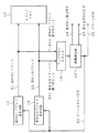
図3は、このような従来のエラスティックストア回路の一例を示すブロック図である。図3において、読み出しアドレス発生回路11は、2ポートメモリ13の図示しない出力ポートより出力すべきデータが蓄積されている2ポートメモリ13内のアドレスを指定する読み出しアドレス21を発生する回路であり、書き込みアドレス発生回路12は、2ポートメモリ13の図示しない入力ポートから入力するデータを蓄積する2ポートメモリ13内のアドレスを指定する書き込みアドレス22を発生する回路であり、それぞれ2ポートメモリ13と減算器17に接続されている。
【0005】
減算器17は、2ポートメモリ13に送出される読み出しアドレス21と書き込みアドレス22をそれぞれモニタして、読み出しアドレス値と書き込みアドレス値を減算することにより両アドレスの距離を算出している。減算器17の算出結果は、減算器17に接続されている距離検出部18に伝達され、距離検出部18では、両アドレスの距離が規定値に達したことを検出すると、イニシャライズ信号23を読み出しアドレス発生回路11と書き込みアドレス発生回路12に送出して各回路を初期状態に設定する。また、このとき距離検出部18は、アラーム信号26を図示しないアラーム受信部に送出して、両アドレスの接近と初期設定が行われたことを通知する。
【0006】
初期状態に設定された読み出しアドレス発生回路11と書き込みアドレス発生回路12では、発生する読み出しアドレスと書き込みアドレスを初期の状態に戻すので、両アドレスの距離は最大値に戻る。
【0007】
【発明が解決しようとする課題】
しかし、上述した従来のエラスティックストア回路では、読み出しアドレスと書き込みアドレスとの距離差を求めて規定値以内か否かを判断するために、2つのアドレスに対して蓄積・演算・比較が必要であり、回路規模構成が大きいという問題がある。
【0008】
また、読み出しアドレスの基準値を中心とする規定値以内の書き込みアドレスという基準値への接近の際に、読み出しアドレス発生回路および書き込みアドレス発生回路に対して初期設定という手段で対応しているために、初期設定する機会頻度が多くなる可能性が高いという問題がある。
【0009】
本発明の目的は、読み出しアドレスと書き込みアドレスとの差を検出する回路を簡素化して回路規模の縮小化を図り、かつ読み出しアドレスと書き込みアドレスとが接近する状態を事前に検知し、初期設定の機会頻度を抑えることができるエラスティックストア回路を提供することにある。
【0010】
【課題を解決するための手段】
本発明は、2ポートメモリと、2ポートメモリに対し一方のポートを介してデータを読み出すための読み出しアドレスを発生する第1のアドレス発生手段と、2ポートメモリに対し他方のポートを介してデータを書き込むための書き込みアドレスを発生する第2のアドレス発生手段とを備え、読み出しアドレスと書き込みアドレスの差が規定値以内に接近した場合に両アドレスの差を補正するエラスティックストア回路において、
前記読み出しアドレスと書き込みアドレスのいずれか一方の最下位ビットをカウントアップ信号とし、他方の最下位ビットをカウントダウン信号として両アドレスの距離差をカウント値として認識するアップダウンカウンタと、
アップダウンカウンタのカウンタ値が、読み出しアドレスと書き込みアドレスとが接近したことを表す所定の第1の規定値に達したことを検出すると、前記第1のアドレス発生手段または第2のアドレス発生手段のいずれか一方のアドレス発生を停止する信号を一定時間出力し、アップダウンカウンタのカウンタ値が、読み出しアドレスと書き込みアドレスとが更に接近したことを表す所定の第2の規定値に達したことを検出すると、前記第1のアドレス発生手段の読み出しアドレスと第2のアドレス発生手段の書き込みアドレスとを最大距離の初期値に設定するイニシャライズ信号を出力する距離検出部と、
を備えることを特徴とする。
【0011】
本発明は、2ポートメモリを使用し、読み出しアドレスと書き込みアドレスの接近を検出し、両アドレスを補正するエラスティックストア回路において、前記の両アドレスの距離差を補正する機能ブロックを、両アドレスの最下位ビットのみを利用したアップダウンカウンタを用いることにより極めて小さな回路規模で実現し、常に両アドレスの距離差をカウンタ値として認識することにより、両アドレスの接近をそのカウンタ値が規定値になることで発見し、読み出しアドレスが書き込みアドレスに追いついた場合は読み出し停止信号を、書き込みアドレスが読み出しアドレスに追いついた場合は書き込み停止信号を出力し、両アドレスの距離を補正することにより、回路がイニシャライズされる頻度を抑えることができる。
【0012】
【発明の実施の形態】
次に、本発明の実施の形態について図面を参照して説明する。
【0013】
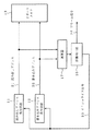
図1は、本発明に係るエラスティックストア回路の実施の形態を示すブロック図である。図1において、読み出しアドレス発生回路11は、2ポートメモリ13の図示しない出力ポートより出力すべきデータが蓄積されている2ポートメモリ13内のアドレスを指定する読み出しアドレス21を発生する回路であり、書き込みアドレス発生回路12は、2ポートメモリ13の図示しない入力ポートから入力するデータを蓄積する2ポートメモリ13内のアドレスを指定する書き込みアドレス22を発生する回路である。
【0014】
読み出しアドレス発生回路11は、2ポートメモリ13とアップダウンカウンタ15に接続されており、アップダウンカウンタ15に接続されるのは、読み出しアドレス21の最下位ビット211のみである。また、書き込みアドレス発生回路12は、2ポートメモリ13とアップダウンカウンタ15に接続されており、アップダウンカウンタ15に接続されるのは、書き込みアドレス22の最下位ビット221のみである。
【0015】
アップダウンカウンタ15は、初期設定時にアドレス値の約半分となる理想距離の半分の値を初期値としてロードし、書き込みアドレス22の最下位ビット221をカウントアップ指示信号として、読み出しアドレス21の最下位ビット211をカウントダウン指示信号として入力し、両アドレスの距離をカウンタ出力値として認識している。このアップダウンカウンタ15は、2アドレスで1カウント動作するため、実際のアドレス間の距離は、カウント値の約2倍の値である。
【0016】
アップダウンカウンタ15は、距離検出部16に接続されており、距離検出部16は、アップダウンカウンタ15のカウンタ値が最小規定値に達したことを検出すると、読み出しアドレスが書き込みアドレスに追いついたことを検出しているので、読み出し停止信号24を、設定した一定時間の間出力する。逆に、カウント値が最大規定値に達したことを検出すると、書き込みアドレスが読み出しアドレスに追いついたことを検出しているので、書き込み停止信号25を、設定した一定時間の間出力する。この制御により、回路がイニシャライズされる頻度は、極端に減らすことができる。
【0017】
読み出し動作か書き込み動作のどちらかが止まってしまったような場合は、上記制御を行ってもカウンタ値は、最小規定値より小さく、あるいは最大規定値より大きくなり、イニシャライズ条件(読み出しアドレスと書き込みアドレスが極端に隣接)に達する。このときは、イニシャライズ信号23を読み出しアドレス発生回路11と書き込みアドレス発生回路12に送出して、各回路を初期状態に設定する。
【0018】
初期状態に設定された読み出しアドレス発生回路11と書き込みアドレス発生回路12では、発生する読み出しアドレスと書き込みアドレスを初期状態に戻すので、両アドレスの距離は最大値に戻される。このとき、回路の異常状態を外部へ通知するために、イニシャライズ信号23をアラーム信号26として外部へ送出する。
【0019】
アップダウンカウンタ15は、カウントアップ指示信号が入力されると1カウントアップし、カウントダウン指示信号が入力されると1カウントダウンする。従って、書き込みデータと読み出しデータの速度差/位相差が大きくない場合は、カウント出力値は、ロード値に近い値をキープすることになる。読み出し/書き込み両アドレスの最下位ビットをカウントアップ/ダウン指示信号に使用しているので、2アドレス変化したときに、1カウントアップ/ダウンすることになる。
【0020】
アップダウンカウンタ15は、読み出し/書き込み両アドレスの最下位ビットのみを使用しているので、アドレス全てを比較する減算器に比べて回路規模を小さくすることが可能である。また、メモリが深くなってアドレス値が大きくなった場合でも、同じ回路で対応できる。よって、アドレス幅が大きい場合には特に有効である。
【0021】
読み出し停止信号24と書き込み停止信号25は、外部で読み出し停止あるいは書き込み停止機能を持っていない場合は、事前アラーム信号として用いることもできる。通常どちらかの制御は行われる構成となるので、片方を停止信号として用い、もう片方をアラーム信号として用いればよい。
【0022】
なお、書き込みアドレス22の最下位ビット221をダウン制御信号、読み出しアドレス21の最下位ビット211をアップ制御信号としても良い。
【0023】
次に、図2を参照して本発明の実施の形態の動作を説明する。
【0024】
図2において、アドレス距離差を検出する距離検出部16は、読み出し停止信号24の出力条件としてのカウント値を検出するmin条件デコード部161と、書き込み停止信号25の出力条件としてのカウント値を検出するmax条件デコード部162と、イニシャライズ条件としてのカウント値を検出するイニシャライズ条件デコード部163と、読み出し停止信号24および書き込み信号25を設定した一定時間の間出力するカウンタ164とを備えている。
【0025】
ここで一例として、2ポートメモリ13のアドレスを0〜127、読み出し停止信号を出力するときの読み出しアドレス21と、書き込み停止信号を出力するときの書き込みアドレス22との距離差を8とし、イニシャライズする条件を距離差2とする。このとき設定する停止信号送出条件とイニシャライズ条件のアドレス距離差は、各エラスティックストア回路における読み出しと書き込みの位相差により両アドレスが接近するであろうアドレスを予測して設定する。
【0026】
距離検出部16は、常に両アドレスの距離差を認識しているので、ぎりぎりの値に設定することも可能であるが、読み出し側/書き込み側にそれぞれイネーブル信号がある場合には、このイネーブル信号によるアドレス距離差の増減を考慮に入れる必要がある。カウントアップ指示信号、カウントダウン指示信号にアドレスの最下位ビットを使用しているため、2アドレスに1回アップあるいはダウンする。カウンタ出力値で1に設定することにより、アドレス距離差としては2を最小値に設定することになる。
【0027】
まず、初期状態においては、両アドレスは、最大距離となるように設定され、例えば、書き込みアドレスを0番地、読み出しアドレスを64番地に設定する。アップダウンカウンタ15には理想距離64の半分の32をロードする。読み出し停止信号24の出力条件はアドレス差で8、アップダウンカウンタ15は2アドレスに1回カウント動作するので、カウント値としては4を設定する。また、書き込み停止信号25の出力条件としてはアドレス差で128−8=120、カウントはその半分で60に設定する。イニシャライズ条件としては、カウント値で1と63を設定する。
【0028】
アップダウンカウンタ15は、初期状態で32をロードし、書き込みアドレス最下位ビット221をカウントアップ指示信号、読み出しアドレス最下位ビット211をカウントダウン指示信号として受ける。最下位ビットをそのまま制御信号として用いているので、書き込みアドレス22が2増えて01と立ち上がりエッジが見えた所で1カウントアップする。読み出しアドレス21が2増えて01と立ち上がりエッジが見えた所で1カウントダウンする動作をする。こうすることで、実際の両アドレスの距離の半分の値がカウンタの出力値として表示されることになる。
【0029】
この実施の形態では、読み出し停止信号24の出力条件をアドレス差8と設定しているので、min条件のカウント値は4に設定する。min条件デコード部161で4を検出すると、読み出し停止信号24を外部へ通知し、読み出し動作を停止させる。このとき、読み出し停止信号24は、アドレス差がちょうど中心に近い値まで戻るように、カウンタ164から56クロック間出力される。こうすることで、書き込み動作が順当に行われると、アドレス値差で56、アップダウンカウンタのカウント値で28、カウント値が離れることになるので、カウント値差が32となり、安定した正常動作状態に戻る。
【0030】
逆に、書き込み停止信号25の出力条件であるmax条件としては、検出カウント値に60を設定する。max条件デコード部162で60を検出すると、書き込み停止信号25を外部へ通知し、書き込み動作を停止させる。このとき、書き込み停止信号は、アドレス値差が中心付近まで戻るように、カウンタ164から56クロック間出力される。こうすることで、60まで上がっていたカウント値は28減り、32となる。こうすることで、アドレス値が最も離れた理想的な状態に戻る。通常は、読み出し停止か書き込み停止のどちらかの機能にしか対応していないので、逆の条件の停止信号は、事前アラーム信号として用いればよい。
【0031】
また、イニシャライズ条件としては、アドレス距離差を2と設定しているので、その半分で1をmin条件とし、63をmax条件とし、それぞれイニシャライズ条件デコード部163でデコードする。もしイニシャライズ条件デコード部163で1あるいは63を検出した場合は、イニシャライズ信号23を、読み出しアドレス発生回路11と書き込みアドレス発生回路12に送出することにより、回路全体を初期状態にリセットする。このとき、アラーム状態を外部に通知するためにアラーム信号26も出力する。
【0032】
具体例として、読み出しアドレス21が32で書き込みアドレス22が48と、読み出しアドレス21が書き込みアドレス22に追いついてきた場合を示す。このとき、読み出しアドレス21は、基準値の64から96増え、書き込みアドレス22は、基準値の0から48増えている。従って、アップダウンカウンタ15の出力値は、32+48/2−96/2=8となる。この場合は、min条件4にはひっかからないので、そのまま正常に動作する。
【0033】
更に、読み出しアドレス21が書き込みアドレス22に追いつき、読み出しアドレス21が52、書き込みアドレス22が60と距離差が8になると、アップダウンカウンタ15のカウント出力値は、32+60/2−116/2=4を示し、読み出し停止条件に当てはまるため、読み出し停止信号24が56クロック間出力され、読み出し動作を止める。この間も書き込み動作は行われるため、書き込みアドレス22は56カウントアップし、116となる。読み出しアドレス21は52のままなので、両者の距離は64離れることになり、正常動作状態に戻る。
【0034】
逆に、書き込みアドレス22が52、読み出しアドレス21が60と、書き込みアドレス22が読み出しアドレス21に追いついた場合は、アップダウンカウンタの出力値は、32+116/2−60/2=60となり、書き込み停止条件となり、書き込み停止信号25が56クロック間出力され、書き込み動作は停止する。この間に読み出しアドレス21は56進み、116となり、両アドレス間の距離は64離れることになる。
【0035】
読み出し動作あるいは書き込み動作のどちらかが停止し、両アドレス間の距離が2になると、アップダウンカウンタ15の出力値から、イニシャライズ条件デコード部163で1あるいは63を検出し、イニシャライズ条件となる。この状態はアラーム状態であるので、イニシャライズ信号23を読み出し、読み出しアドレス発生回路11と書き込みアドレス発生回路12に出力し、回路全体を初期状態に戻し、アラーム信号26を外部へ出力する。
【0036】
【発明の効果】
以上説明したように、本発明によれば、読み出しアドレスと書き込みアドレスの接近を判断し初期設定するエラスティック回路のアドレス制御部を非常に小さな回路規模で実現することが可能となる。アドレスの距離検出には最下位ビットのみを使用するので、メモリの深さ(アドレス値の大きさ)に関係なく、同じ小規模の回路で実現できる。
【0037】
また、両アドレス間の距離を観測し、読み出し停止信号あるいは書き込み停止信号を出力することで、両アドレス間の距離を補正するため、簡単にイニシャライズされることがなくなる。読み出し停止/書き込み停止双方の機能を外部回路で実現していることは少ないが、片方の制御のみでイニシャライズされる頻度は格段に減らすことができる。使用しないもう片方の停止信号は事前アラーム信号として使用すればよい。
【0038】
また、両アドレスの最下位ビットをアップダウンカウンタに入力しているため、アップダウンカウンタの動作スピードは、読み出し/書き込みクロックの半分となり、低消費電力化にも貢献する。
【図面の簡単な説明】
【図1】本発明に係るエラスティックストア回路の実施の形態を示すブロック図である。
【図2】本発明に係るエラスティックストア回路の動作を説明するブロック図である。
【図3】従来のエラスティックストア回路の一例を示すブロック図である。
【符号の説明】
11 読み出しアドレス発生回路
12 書き込みアドレス発生回路
13 2ポートメモリ
15 アップダウンカウンタ
16,18 距離検出部
17 減算器
21 読み出しアドレス
22 書き込みアドレス
23 イニシャライズ信号
24 読み出し停止信号
25 書き込み停止信号
26 アラーム信号
161 min条件デコード部
162 max条件デコード部
163 イニシャライズ条件デコード部
164 カウンタ
211 読み出しアドレス最下位ビット
221 書き込みアドレス最下位ビット[0001]
BACKGROUND OF THE INVENTION
In the present invention, when a two-port memory that reads data written to the first port from the second port is used, the proximity between the read address and the write address is detected, and the two addresses are set to the initial values to correct. In particular, the present invention relates to an elastic store circuit that can detect that an address has approached a predetermined value or more with a simple circuit and can suppress the frequency of initial setting.
[0002]
[Prior art]
With the demand for higher speed and higher functionality of digital data transmission systems, higher speed and higher functionality are required for elastic memory circuits for data speed conversion or delay adjustment. For this reason, an elastic memory circuit using a two-port memory with independent input / output ports has been used.
[0003]
In such an elastic memory circuit, since the write operation and the read operation are performed by independent clocks, the approach of the write address of the read address due to the phase shift of each clock is detected in advance, Control that corrects the read address so that it does not overtake the write address is required, and the reduction in circuit scale has become important.
[0004]
FIG. 3 is a block diagram showing an example of such a conventional elastic store circuit. In FIG. 3, a read
[0005]
The subtractor 17 monitors the read address 21 and the write address 22 sent to the 2-
[0006]
In the read
[0007]
[Problems to be solved by the invention]
However, the above-described conventional elastic store circuit requires accumulation, calculation, and comparison with respect to two addresses in order to determine the distance difference between the read address and the write address and determine whether or not it is within a specified value. There is a problem that the circuit scale configuration is large.
[0008]
In addition, when approaching a reference value called a write address within a specified value centered on the reference value of the read address, the read address generation circuit and the write address generation circuit are handled by means of initial setting. There is a problem that there is a high possibility that the frequency of initial setting is increased.
[0009]
An object of the present invention is to simplify a circuit for detecting a difference between a read address and a write address to reduce the circuit scale, detect in advance a state where the read address and the write address are close, and perform initial setting. An object of the present invention is to provide an elastic store circuit that can suppress the frequency of opportunities.
[0010]
[Means for Solving the Problems]
The present invention relates to a two-port memory, a first address generating means for generating a read address for reading data from one port to the two-port memory, and a data to the two-port memory via the other port. An elastic store circuit for correcting a difference between both addresses when a difference between the read address and the write address approaches within a specified value, and a second address generating means for generating a write address for writing
An up / down counter that recognizes a distance difference between both addresses as a count value using the least significant bit of either the read address or the write address as a count up signal and the other least significant bit as a count down signal;
When it is detected that the counter value of the up / down counter has reached a predetermined first prescribed value indicating that the read address and the write address have approached, the first address generating means or the second address generating means Outputs a signal to stop the generation of one of the addresses for a certain period of time, and detects that the counter value of the up / down counter has reached a predetermined second specified value indicating that the read address and the write address are closer Then, a distance detector that outputs an initialization signal for setting the read address of the first address generator and the write address of the second address generator to an initial value of the maximum distance ;
It is characterized by providing.
[0011]
The present invention uses a two-port memory, detects an approach between a read address and a write address, and corrects both addresses in an elastic store circuit that corrects the distance difference between the two addresses. By using an up / down counter that uses only the least significant bit, it is realized with an extremely small circuit scale, and by always recognizing the distance difference between both addresses as a counter value, the counter value becomes the specified value for the approach of both addresses. When the read address catches up with the write address, a read stop signal is output. When the write address catches up with the read address, a write stop signal is output, and the circuit is initialized by correcting the distance between the two addresses. Can be suppressed.
[0012]
DETAILED DESCRIPTION OF THE INVENTION
Next, embodiments of the present invention will be described with reference to the drawings.
[0013]
FIG. 1 is a block diagram showing an embodiment of an elastic store circuit according to the present invention. In FIG. 1, a read
[0014]
The read
[0015]
The up / down
[0016]
The up / down
[0017]
If either the read operation or the write operation stops, the counter value is smaller than the minimum specified value or larger than the maximum specified value even if the above control is performed, and the initialization condition (read address and write address) Reach the extreme). At this time, an initialization signal 23 is sent to the read
[0018]
In the read
[0019]
The up / down counter 15 counts up by 1 when a count-up instruction signal is input, and counts down by 1 when a count-down instruction signal is input. Therefore, when the speed difference / phase difference between the write data and the read data is not large, the count output value keeps a value close to the load value. Since the least significant bit of both the read / write addresses is used for the count up / down instruction signal, the count is incremented / decreased by 1 when two addresses are changed.
[0020]
Since the up / down counter 15 uses only the least significant bit of both the read / write addresses, it is possible to reduce the circuit scale as compared with a subtractor that compares all addresses. Even when the memory becomes deep and the address value becomes large, the same circuit can be used. Therefore, it is particularly effective when the address width is large.
[0021]
The read stop signal 24 and the write stop signal 25 can also be used as a pre-alarm signal when there is no read stop or write stop function externally. Since one of the controls is usually performed, one of them may be used as a stop signal and the other may be used as an alarm signal.
[0022]
Note that the least significant bit 221 of the write address 22 may be a down control signal, and the least significant bit 211 of the read address 21 may be an up control signal.
[0023]
Next, the operation of the embodiment of the present invention will be described with reference to FIG.
[0024]
In FIG. 2, the
[0025]
Here, as an example, the address of the 2-
[0026]
Since the
[0027]
First, in the initial state, both addresses are set to have the maximum distance. For example, the write address is set to address 0 and the read address is set to address 64. The up / down
[0028]
The up / down counter 15 loads 32 in the initial state, and receives the write address least significant bit 221 as a count up instruction signal and the read address least significant bit 211 as a count down instruction signal. Since the least significant bit is used as a control signal as it is, the write address 22 is increased by 2 and incremented by 1 when the rising edge is seen as 01. The read address 21 is incremented by 2 and an operation of counting down by 1 is performed when the rising edge is seen as 01. By doing so, half the distance between the actual addresses is displayed as the output value of the counter.
[0029]
In this embodiment, since the output condition of the read stop signal 24 is set to the address difference 8, the count value of the min condition is set to 4. When 4 is detected by the min
[0030]
On the contrary, 60 is set to the detection count value as the max condition that is the output condition of the write stop signal 25. When the max
[0031]
Further, since the address distance difference is set to 2 as the initialization condition, half of the difference is set to 1 as the min condition and 63 as the max condition, and the initialization
[0032]
As a specific example, the read address 21 is 32, the write address 22 is 48, and the read address 21 has caught up with the write address 22. At this time, the read address 21 is increased by 96 from the reference value of 64, and the write address 22 is increased by 48 from the reference value of 0. Therefore, the output value of the up / down
[0033]
Further, when the read address 21 catches up with the write address 22 and the read address 21 is 52 and the write address 22 is 60 and the distance difference is 8, the count output value of the up / down
[0034]
Conversely, if the write address 22 is 52, the read address 21 is 60, and the write address 22 catches up with the read address 21, the output value of the up / down counter is 32 + 116 / 2-60 / 2 = 60, and the write is stopped. As a condition, the write stop signal 25 is output for 56 clocks, and the write operation stops. During this time, the read address 21 advances 56 and becomes 116, and the distance between the two addresses is 64.
[0035]
When either the read operation or the write operation is stopped and the distance between the two addresses becomes 2, the initialization
[0036]
【The invention's effect】
As described above, according to the present invention, it is possible to realize an address control unit of an elastic circuit that determines the proximity between a read address and a write address and performs initialization with a very small circuit scale. Since only the least significant bit is used for address distance detection, it can be realized with the same small circuit regardless of the memory depth (address value size).
[0037]
Further, since the distance between both addresses is corrected by observing the distance between both addresses and outputting a read stop signal or a write stop signal, the initialization is not easily performed. Although it is rare that both the read stop / write stop functions are realized by an external circuit, the frequency of initialization can be significantly reduced by only one control. The other stop signal that is not used may be used as a prior alarm signal.
[0038]
In addition, since the least significant bit of both addresses is input to the up / down counter, the operation speed of the up / down counter is half that of the read / write clock, contributing to low power consumption.
[Brief description of the drawings]
FIG. 1 is a block diagram showing an embodiment of an elastic store circuit according to the present invention.
FIG. 2 is a block diagram for explaining the operation of the elastic store circuit according to the present invention.
FIG. 3 is a block diagram showing an example of a conventional elastic store circuit.
[Explanation of symbols]
11 Read address generating
Claims (6)
前記読み出しアドレスと書き込みアドレスのいずれか一方の最下位ビットをカウントアップ信号とし、他方の最下位ビットをカウントダウン信号として両アドレスの距離差をカウント値として認識するアップダウンカウンタと、
アップダウンカウンタのカウンタ値が、読み出しアドレスと書き込みアドレスとが接近したことを表す所定の第1の規定値に達したことを検出すると、前記第1のアドレス発生手段または第2のアドレス発生手段のいずれか一方のアドレス発生を停止する信号を一定時間出力し、アップダウンカウンタのカウンタ値が、読み出しアドレスと書き込みアドレスとが更に接近したことを表す所定の第2の規定値に達したことを検出すると、前記第1のアドレス発生手段の読み出しアドレスと第2のアドレス発生手段の書き込みアドレスとを最大距離の初期値に設定するイニシャライズ信号を出力する距離検出部と、
を備えることを特徴とするエラスティックストア回路。A 2-port memory, a first address generating means for generating a read address for reading data from one port to the 2-port memory, and a data for writing data to the 2-port memory via the other port In an elastic store circuit comprising a second address generating means for generating a write address, and correcting a difference between both addresses when the difference between the read address and the write address approaches within a specified value,
An up / down counter that recognizes a distance difference between both addresses as a count value using the least significant bit of either the read address or the write address as a count up signal and the other least significant bit as a count down signal;
When it is detected that the counter value of the up / down counter has reached a predetermined first prescribed value indicating that the read address and the write address have approached, the first address generating means or the second address generating means Outputs a signal to stop the generation of one of the addresses for a certain period of time, and detects that the counter value of the up / down counter has reached a predetermined second specified value indicating that the read address and the write address are closer Then, a distance detector that outputs an initialization signal for setting the read address of the first address generator and the write address of the second address generator to an initial value of the maximum distance ;
An elastic store circuit comprising:
読み出しアドレスと書き込みアドレスのいずれか一方の最下位ビットをカウントアップ信号とし、他方の最下位ビットをカウントダウン信号として両アドレスの距離差をカウント値として認識し、前記カウンタ値が、読み出しアドレスと書き込みアドレスとが接近したことを表す所定の第1の規定値に達したことを検出すると、前記読み出しアドレスまたは書き込みアドレスの発生を停止して読み出しアドレスと書き込みアドレスの差を所定の距離に設定し、前記読み出しアドレスと書き込みアドレスとが更に接近したことを表す所定の第2の規定値に達したことを検出すると、前記読み出しアドレスと書き込みアドレスの差を最大距離の初期値に設定することを特徴とするエラスティックストア回路のアドレス補正方法。In an address correction method for an elastic store circuit that uses a two-port memory, detects an approach between a read address and a write address, and corrects both addresses,
The least significant bit of either the read address or the write address is used as a count-up signal, the other least significant bit is used as a count-down signal, and the distance difference between the two addresses is recognized as a count value. , The generation of the read address or the write address is stopped, and the difference between the read address and the write address is set to a predetermined distance. When it is detected that a predetermined second prescribed value indicating that the read address and the write address are further closer is detected, a difference between the read address and the write address is set to an initial value of a maximum distance. Elastic store circuit address correction method.
Priority Applications (1)
| Application Number | Priority Date | Filing Date | Title |
|---|---|---|---|
| JP2000142899A JP3772639B2 (en) | 2000-05-16 | 2000-05-16 | Elastic store circuit |
Applications Claiming Priority (1)
| Application Number | Priority Date | Filing Date | Title |
|---|---|---|---|
| JP2000142899A JP3772639B2 (en) | 2000-05-16 | 2000-05-16 | Elastic store circuit |
Publications (2)
| Publication Number | Publication Date |
|---|---|
| JP2001325790A JP2001325790A (en) | 2001-11-22 |
| JP3772639B2 true JP3772639B2 (en) | 2006-05-10 |
Family
ID=18649794
Family Applications (1)
| Application Number | Title | Priority Date | Filing Date |
|---|---|---|---|
| JP2000142899A Expired - Fee Related JP3772639B2 (en) | 2000-05-16 | 2000-05-16 | Elastic store circuit |
Country Status (1)
| Country | Link |
|---|---|
| JP (1) | JP3772639B2 (en) |
-
2000
- 2000-05-16 JP JP2000142899A patent/JP3772639B2/en not_active Expired - Fee Related
Also Published As
| Publication number | Publication date |
|---|---|
| JP2001325790A (en) | 2001-11-22 |
Similar Documents
| Publication | Publication Date | Title |
|---|---|---|
| US6825703B1 (en) | Delay locked loop and method of driving the same | |
| US7793172B2 (en) | Controlled reliability in an integrated circuit | |
| US6886120B2 (en) | Memory control circuit | |
| US7511546B2 (en) | Synchronous memory device with output driver controlller | |
| JP3772639B2 (en) | Elastic store circuit | |
| US7593285B2 (en) | Semiconductor memory device with delay locked loop | |
| US8482326B2 (en) | DLL circuit, semiconductor device including the same, and data processing system | |
| US20230015113A1 (en) | Impedance calibration circuit, impedance calibration method, and memory | |
| US6898725B2 (en) | Method for adjusting system clocks using dynamic clock ratio detector to detect clock ratio between clock domain of driver and counting receiver clock domain | |
| US7013401B2 (en) | Processor capable of preventing sleep/hold state based on a difference between a processing block address and a writing block address | |
| JPH04259997A (en) | Semiconductor integrated circuit | |
| JP3598883B2 (en) | Elastic store circuit | |
| KR100790992B1 (en) | Duty cycle correction circuit and duty cycle correction method using delay cells | |
| CN112291682B (en) | Sound playing device and sound playing system | |
| JP3097672B2 (en) | Memory control circuit | |
| JPH1091394A (en) | Input and output controller | |
| US6201487B1 (en) | Error detecting circuit in a line length decoding system | |
| US12327606B2 (en) | Semiconductor device | |
| JPH08237254A (en) | Oam cell inserting device | |
| JP2912367B1 (en) | Computer readable medium recording a PLL circuit and a PLL program | |
| US8245121B2 (en) | Signal control circuit and signal control apparatus | |
| JP2550925B2 (en) | Elastic store circuit | |
| JPH07250101A (en) | Elastic storage circuit | |
| KR100888337B1 (en) | Chip reset circuit | |
| KR100273310B1 (en) | Sense amp control circuit with low power dissipation |
Legal Events
| Date | Code | Title | Description |
|---|---|---|---|
| A131 | Notification of reasons for refusal |
Free format text: JAPANESE INTERMEDIATE CODE: A131 Effective date: 20050315 |
|
| A521 | Written amendment |
Free format text: JAPANESE INTERMEDIATE CODE: A523 Effective date: 20050509 |
|
| TRDD | Decision of grant or rejection written | ||
| A01 | Written decision to grant a patent or to grant a registration (utility model) |
Free format text: JAPANESE INTERMEDIATE CODE: A01 Effective date: 20060124 |
|
| A61 | First payment of annual fees (during grant procedure) |
Free format text: JAPANESE INTERMEDIATE CODE: A61 Effective date: 20060206 |
|
| R150 | Certificate of patent or registration of utility model |
Free format text: JAPANESE INTERMEDIATE CODE: R150 |
|
| FPAY | Renewal fee payment (event date is renewal date of database) |
Free format text: PAYMENT UNTIL: 20100224 Year of fee payment: 4 |
|
| FPAY | Renewal fee payment (event date is renewal date of database) |
Free format text: PAYMENT UNTIL: 20100224 Year of fee payment: 4 |
|
| FPAY | Renewal fee payment (event date is renewal date of database) |
Free format text: PAYMENT UNTIL: 20110224 Year of fee payment: 5 |
|
| LAPS | Cancellation because of no payment of annual fees |