JP3770558B2 - Light guide plate - Google Patents
Light guide plate Download PDFInfo
- Publication number
- JP3770558B2 JP3770558B2 JP2002010878A JP2002010878A JP3770558B2 JP 3770558 B2 JP3770558 B2 JP 3770558B2 JP 2002010878 A JP2002010878 A JP 2002010878A JP 2002010878 A JP2002010878 A JP 2002010878A JP 3770558 B2 JP3770558 B2 JP 3770558B2
- Authority
- JP
- Japan
- Prior art keywords
- light
- guide plate
- light guide
- incident
- illumination
- Prior art date
- Legal status (The legal status is an assumption and is not a legal conclusion. Google has not performed a legal analysis and makes no representation as to the accuracy of the status listed.)
- Expired - Fee Related
Links
Images


Classifications
-
- G—PHYSICS
- G02—OPTICS
- G02B—OPTICAL ELEMENTS, SYSTEMS OR APPARATUS
- G02B6/00—Light guides; Structural details of arrangements comprising light guides and other optical elements, e.g. couplings
- G02B6/0001—Light guides; Structural details of arrangements comprising light guides and other optical elements, e.g. couplings specially adapted for lighting devices or systems
- G02B6/0011—Light guides; Structural details of arrangements comprising light guides and other optical elements, e.g. couplings specially adapted for lighting devices or systems the light guides being planar or of plate-like form
- G02B6/0013—Means for improving the coupling-in of light from the light source into the light guide
- G02B6/0015—Means for improving the coupling-in of light from the light source into the light guide provided on the surface of the light guide or in the bulk of it
- G02B6/0016—Grooves, prisms, gratings, scattering particles or rough surfaces
-
- G—PHYSICS
- G02—OPTICS
- G02B—OPTICAL ELEMENTS, SYSTEMS OR APPARATUS
- G02B6/00—Light guides; Structural details of arrangements comprising light guides and other optical elements, e.g. couplings
- G02B6/0001—Light guides; Structural details of arrangements comprising light guides and other optical elements, e.g. couplings specially adapted for lighting devices or systems
- G02B6/0011—Light guides; Structural details of arrangements comprising light guides and other optical elements, e.g. couplings specially adapted for lighting devices or systems the light guides being planar or of plate-like form
- G02B6/0066—Light guides; Structural details of arrangements comprising light guides and other optical elements, e.g. couplings specially adapted for lighting devices or systems the light guides being planar or of plate-like form characterised by the light source being coupled to the light guide
- G02B6/0068—Arrangements of plural sources, e.g. multi-colour light sources
Description
【0001】
【発明の属する技術分野】
この発明は例えば液晶パネルを背面より照射する面状光源に用いられる導光板に関する。
【0002】
【従来の技術】
近年、ブック型のワードプロセッサやコンピュータ、又は携帯電話機、携帯TVのような小型、薄型の情報機器の表示装置として、薄型でしかも見易いバックライト機構を有する液晶表示装置が用いられている。このようなバックライト機構としては、液晶パネルを背後から全面にわたり照射する面状光源が用いられており、この面状光源としては蛍光ランプ又はLED(発光ダイオード)よりなる発光源と、その光束を液晶パネルに照射する面状の光束に変換する導光板よりなるものが一般的である。この中で、特に近年は、更なる小型、薄型化と長寿命化を目的として発光源としてLEDを用いた面状光源が多く使用されるようになってきている。
【0003】
このようなバックライトから均一な照明光を得るには、発光源は均質な線状の光源であることが望ましい。しかしながら、発光源としてLEDを用いる場合には費用等の関係から使用できるLEDの個数が制限される。図5はLEDを平面形状が矩形の導光板の側面に対向して設けてなる従来のエッジライト式のバックライトを示す図である。(a)は斜視図、(b)は側面図である。
【0004】
図5において、110はバックライトであり、導光板101と発光源として3個のLED102を有している。導光板101は無色透明なプラスチック材等の透光部材よりなる板状で略直方体形状をしており、その上面101aを光出射面とし、これと対向する下面101bには、発光源であるLED102からの光を前記光出射面101aに向けて反射させるための手段として、その表面に複数の微小なシボ又は複数個の半球状ドット等を有する光拡散面が形成されている。LED102は導光板101の入光側面101cに対向する位置に配設され、図示しない駆動回路より所定の電流が供給されて、LED102の材質で出決まる所定の色の光を発光、出射する。LED102からの出射光は入光側面101cから導光板101に入り、大部分の光は上面101aである光出射面で全反射、下面101bである光拡散面では全反射又は乱反射を1回又は複数回行った後に上面101aである光出射面より照明光105として外部に出射する。外部に出射した照明光105は(b)に示すように液晶パネル107を背後から照明する。なお、前記面状の照明光の輝度の均一性を確保するために上記下面101b内のシボの粗さを調整したり、半球状ドットの形状、密度を場所により変えたりする。
【0005】
【発明が解決しようとする課題】
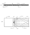
このようにして、小型、薄型のバックライトにより液晶パネルの照明がなされる。しかしながら、上記の面状光源においては、以下に述べるような問題点がある。図6は、図5に示した導光板101を説明の便宜上モデル化して表した図であり、(a)は平面図、(b)は側面図である。図6(b)に示すようにモデル化された導光板101の下面101bはシボ等の凹凸がなく、拡散面でなく平滑な面となっている。次に、図7は図6に示すモデル化された導光板101の中にLED102から入り込んだ光の分布の状態を示す平面図であり、図7(a)は全体の状態を示す図、図7(b)はLED102付近の拡大図である。図6および図7において、101cは入光側面、101dは左側面、101fは右側面、101eは前記入光側面101cに対向する対向側面である。
【0006】
図7に示すようにLED102は導光板101に対し極めて近接して配置されている。これは、LED102の発光による入射光s1を効率よく導光板101に取り込むためである。ここで、導光板の材質は透光性のアクリルであり、その屈折率は略 1.5 であり、臨界角は略42゜である。前記LED102の発光は入射光s1として入光側面101cに達し屈折によりこの面を透過し導光板101内部に透過による内部光sとして出射する。このときの出射角は入射角よりも小となり、理論的には最大でも臨界角(略42゜)となり、実際には最大で30゜程度となる。このような事情から図7(a)に示すように導光板101の内部に内部光sの存在しない無効領域Rを生ずる。この無効領域Rは最大の出射角を有する内部光(s)により決まり、境界の傾角θ1は略60°となる。
【0007】
この無効領域Rにおいては内部光sが存在しないため、導光板101の役割である光路変換作用が行われず、照明光(図5の105)が出射することが殆ど行われない。なお、無効領域R以外の領域においては、内部光sが出射角に応じて、前記の左側面101d、右側面101f又は対向側面101eに到達し、左側面101dまたは、右側面に達した光は全反射により対向側面101eに到達する。このようにして導光板101に広く分布する。そして、実際にはこのような分布の過程で、図5に示すような下面101bの拡散面に入射して乱反射され、上面101a(図6(b))から照明光として出射することになる。そして実際には、上記下面101b内のシボの粗さを調整したりすることにより、光の分布する領域の照明光の輝度を均一化することができる。しかしながら、上記したように前記無効領域Rからは照明光は殆ど出射せず、その範囲の大きさも無視できない。よって、導光板101全体として見た場合には、その出射する照明光(5)の輝度ムラを生じ、照明の対象となる液晶パネル(図5の7)の表示品質を低下させることとなる。
【0008】
次に、図8は図6に示すモデル化された導光板101の中にLED102から入り込んだ光の分布の状態を示す側面図であり、図8(a)は全体の状態を示す図、図8(b)はLED102付近の拡大図である。図8(b)に示すようにLED102から発して入光側面1cに達した入射光s1はすでに説明した原理により、この面を透過して、実際には最大でも30°程度の出射角で透過して内部光sとして導光板内に入り、図8(a)に示すように上面101aと下面101bの間で反射を繰り返し、導光板内101内に広く分布し、分布した領域では、すでに説明した原理により照明光を出射する。しかし、図8(b)に示すように、入光側面1cの近傍には内部光sの存在しない無効領域R1が存在し、この領域からは照明光が生じないし又この領域の大きさも無視できない。よって、側面的に見ても、照明光に無視できない輝度ムラを生ずることとなる。
【0009】
このように、LEDを発光源とする従来のバックライトの導光板においては、平面的に見ても側面的に見ても導光板の入光端面の近傍に照明光を生じない無効領域が無視できない大きさで存在し、このため、照明光の輝度ムラを生ずるという問題があった。本発明はこのような問題を解決し、導光板から発する照明光の輝度の均一性を向上することを課題とする。
【0010】
【課題を解決するための手段】
上記の課題を解決するための第1の手段として本発明は、板状の透光材よりなり、その側面に対向して配された発光光源からの光を光路変換してその上面から照明対象物に対し面状の照明光を出射する導光板において、前記発光光源と対向する導光板の入光側面に、当該側面に開口部を有する穴であって、上下の壁面および左右の壁面と、開口部に対向する奥の壁面と、左右の壁面と奥の壁面の間を接続する 1 対の円弧状の湾曲壁面とにより穴の内面が構成され、上方から見た平面形状は角部が丸められたコ字型をなす穴を複数個設けたことを特徴とする。
【0011】
上記の課題を解決するための第2の手段として本発明は、入光側面に設けた複数の穴は導光板の厚味方向に関し複数層に分かれて設けられていることを特徴とする。
【0014】
上記の課題を解決するためにその第5の手段として本発明は、前記第1の手段第4の手段のいずれかにおいて、前記導光板の下面には複数の溝又はシボが設けられ、光散乱面が形成されていることを特徴とする。
【0015】
【発明の実施の形態】
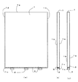
以下に、図面に基づいて本発明の実施の形態を詳細に説明する。図1は本発明の実施の形態に係る導光板を用いたバックライトを示す図であり、(a)は斜視図、(b)は側面図である。図1において、10はバックライトであり、導光板1と発光源として3個のLED2を有している。導光板1は透光性を有するプラスチック材等よりなり、板状で略直方体の形状をなしている。1aは前記導光板1の上面であり光出射面となる。1bは前記導光板1の下面であり、発光源であるLED2からの光を光出射面である前記上面1aに向けて反射させるための手段として、その表面に複数の微小なシボ又は複数個の半球状ドット等を有する光拡散面が形成されている。LED2は導光板の入射端面1cに対向する位置に、その入射端面1cに近接して配置されている。入射端面1cには後に詳述する盲穴3が設けられている。図示しない駆動回路より所定の電流が供給されると、LED2はその材質で決まる所定の色の光を発光、出射する。LED2からの出射光は前記入射端面1cを透過して導光板1内に入り、ここで、上面1aと下面1bの間で反射を繰り返して導光板1内を伝播しながら、その途中で下面からの乱反射により、上面1aを透過した光が、その上面1aより照明光5として出射する。導光板1の上面1aから出射した照明光5は図1(b)に示すように液晶パネル7を背後から照明する。
【0016】
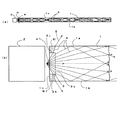
図2は図1に示した前記導光板1の形状をモデル化した導光板1を用いたバックライトを示す図である。即ち、説明の都合上、導光板1の下面1bは図1の場合と異なり、シボ等の凹凸のない平滑な面となっている。図2において、(a)は平面図、(b)および(c)は側面図である。図2において、1cは導光板1の入光側面、1dは左側面、1fは右側面、1eは前記入光側面1cに対向する対向側面である。3は導光板1の入光側面1cに設けられた盲穴である。盲穴3の詳しい形状については後に述べるが、(b)又は(c)に示すように導光板1の厚みに対し一部分だけ盲穴3の掘り込みがある。(b)は厚みに対し2ヶ所の掘り込みがある場合を示し、(c)は1ヶ所の掘り込みがある場合を示す。図2に示すようにLED2は導光板1に対し極めて近接して配置されている。これは、LED2の発光による入射光s1を効率よく導光板1に取り込むためである。ここで、導光板1の材質は透光性のアクリルであり、その屈折率は略 1.5 であり、臨界角は略42゜である。図3は図2に示す導光板1にLED2から透過により内部に入った光sの分布状態を示す平面図であり、(a)は全体図、(b)はそのLED2の近傍の拡大図である。次に、図4は図2に示す導光板1に入った光の分布状態を示す側面図であるが、これについては後に詳述する。 図3(a)に示す光路(光の分布)は、便宜上、導光板の下面1bにおける乱反射は行われず、境界において、全反射又は透過が行われると仮定して示したものである。なお、このよう仮定を行っても全体的な傾向は実際(図1の場合)と近似することが経験上認められている。
【0017】
図3(b)に示すように、入光側面1cに設けられた盲穴3は導光板1の入光側面1cにおいて開口する開口部3b、開口部3bに対向する奥壁部3c、開口部3bの左右の左壁部3d、右壁部3fと、左壁部3dと奥壁部3cを接続する円弧状の左円弧壁部3r1、右壁部3fと奥壁部3cを接続する円弧状の右円弧壁部3r2と、後述する図4(b)に示す盲穴3の上面の壁をなす上壁部3jおよび、盲穴3の下面の壁をなす下壁部3kを有している。
【0018】
LED2の発光による入射光s1のうち盲穴3の奥壁部3cに達したものは、入光側面1cから見て、割合小さな出射角で透過して、導光板の内部の光sとなる。これは、入射光s1のうち入光側面1cに対する入射角が比較的小さいものが入光側面1cと平行な奥壁部3cに達する傾向があり、屈折により入光側面1cに対する入射光s1の入射角よりも小さな出射角で透過して内部光sとなるためである。
【0019】
入射光s1のうち盲穴3のc左円弧壁部3cr1又は右円弧壁部3r2に達したものは、あまり屈折せずに透過して導光板1の内部に入る。これは、入射光s1のうち、入光側面1cに対する入射角が中位の大きさのものが、左円弧壁部3cr1又は右円弧壁部3cr1に入射する傾向があるが、この場合の入射の方向がこれらの円弧壁部の法線の方向と近くなるためである。この結果、入光側面1cから見て発光s1の入射角と近い出射角で透過して内部光sとして導光板の内部に入る。これを、図7に示す従来の場合と比較すると、光線の屈折による内側への折れ曲がりが無くなり、出射光であるsは入射光s1の略延長上となり、出射光sは従来よりも外側に開いた状態となる。
【0020】
入射光s1のうち入光側面1cから見た入射角が比較的大きなものが盲穴3の左壁部3d又は右壁部3fに達する。この場合、入射光s1は左右の壁部3d、3fの法線に対する角度が減少する方向に屈折してsとして出射する。すなわち、内部光sは入射光s1に対し外側に折れ曲がった状態となる。これを、図7に示す従来の場合と比較すると、光の内側への折れ曲がりがなくなり、逆に外側への折れ曲がりを生じ、屈折による出射光である内部光sの角度範囲は従来よりも大幅に拡大する。この結果、一番外側に開いた内部光sの入光側面1cに対する傾角θ1は従来よりも顕著に減少し、これに対応して決まる内部光sの存在しない無効領域R(図3(a)に示す。)の面積は従来よりも大幅に減少する。なお、上記光線の外側への折れ曲がり非常に大きい場合は、出射光は隣の盲穴3のコーナー部で反射され内側に折れ曲がる。このようにして、出射光としての内部光sは従来よりも大幅に広い出射角の範囲にわたって適切に分布する。
【0021】
このようにして、透過により、導光板1内に広い角度範囲で入った内部光sは図3(a)に示すように、透過の際の出射角に応じ左右の側面1d、1f又は対向側面1eのいずれかに達し、ここでこれら側面に対する入射角が臨界角(略42°)以上の場合は全反射され他の側面に達し、ここでさらに側面に対する入射角が臨界角以上であれば更に他の側面に向かって全反射される。このようにして、内部光sが前記の無効領域Rを除き導光板1の全体にわたり広がる。これら内部光sの存在する領域においては、図1に示す実際の場合は、下面(1b)の散乱面の効果により内部光sが乱反射されて導光板の上面より均一な照明光を出射する。本実施の形態においては前記の無効領域Rの面積はすでに述べたように従来よりも大幅に減少している。又、無効領域Rにおいても、内部光sの存在する領域からの乱反射による回りこみにより、その周辺に近い部分は照明光を出射することとなり、照明光を出射しない領域は更に減少する。
【0022】
このようにして本実施の形態においては、平面的に見た場合、実質的に照明光を出射しない領域は従来よりも大幅に低減し、照明光の輝度の均一化が向上する。更には、透過光(内部光s)の前記出射角の制限解除の二次的な効果として、内部光sの入光側面1cに対する出射角が45°付近のものが出現し、これが導光板1の他の側面1d、1e、1fにおいて全反射を繰り返した後に点線s2で示すように入光端面1cに戻る際前記無効領域Rに入り、これによって無効領域Rの輝度が若干向上する効果もある。このように、本実施の形態を平面的に見た場合、従来よりも照明光の輝度の均一性を大幅に向上することのできる条件を備えている。又、無効領域Rが縮小することにより、全体の照明の明るさも向上する。
【0023】
次に、図4は図2に示す導光板1の内部にLED2から入った内部光sの分布状態を示す側面図であり、(a)は全体を示す図であり、(b)はLED2の近傍を示す拡大図である。図4(b)に示すように、LED2からの入射光s1で盲穴3の上壁部3jに達したものは、屈折により顕著に上方に折れ曲がり、内部光sとして導光板1の上面1aに達する。又、入射光s1で盲孔3の下壁部3kに達したものは屈折により顕著に下方に折れ曲がり導光板1の下面に1bに達する。これを図8(b)に示す従来の場合と比較すると光線の折れ曲がりの方向が逆になっており、入光側面1cを基準にとると、内部光sの出射角の最大値が従来より大幅に増加し、この結果内部光sの存在しない無効領域R1の大きさが従来よりも大幅に減少する。これは、従来のように盲孔3がない場合は、入射光は入光側面に対しその法線(水平方向)に近づく方向に折れ曲がるので、上方又は下方への角度が減少するように折れ曲がる。これに対し本実施の形態において盲孔3の上壁部3j及び下壁部3kの法線は垂直方向となっているので、これらの部分に入射した光は屈折によりこれらの法線(垂直方向)に近づくように折れ曲がり、結局、上方または下方への角度が増加するように折れ曲がることとなるからである。
【0024】
このようにして、導光板1の上面1aおよび下面1bに達した光は、本実施の形態の場合はこれらの面に対する入射角が臨界角以上となりこれらの面を屈折により透過し、外部へ出射する。上面1aから外部へ出射した場合は照明光5となる。又下面1bに臨界角以上で入射した光は実際には全部透過して外部に出射するものではなく、そのかなりの部分は図1の1bに示すような散乱面によって乱反射され、上面1aから照明光として出射する。これらの効果により、入光側面1cの近傍においても、前記の無効領域R1以外の部分においては確実に照明光が発生する。
【0025】
次に、LED2からの入射光s1で盲孔3の上壁部3j又は下壁部3k以外の壁部である基部奥壁部3c等に達したものは、屈折により、従来と同様に内側に折れ曲がり、比較的小さな出射角の内部光sとなって、導光板1の上面1a又は下面1aに達し、ここで全反射されて対向面に向かう。以後、上面1a又と下面1aの間で全反射を繰り返すことにより、内部光sが図4(a)に示すように無効領域R1を除き導光板11の全体にわたり分布する。ここで下面1aに達した光束のかなりの部分は、実際には前記の散乱面に乱反射され、上面1aから照明光として出射する。すなわち、側面的に見た場合、無効領域R1以外の部分においては、散乱面の効果により、出射光である照明光の輝度は十分に均一化されており、且つ、無効領域R1の大きさは上記したように従来よりも大幅に縮小された状態となっている。よって側面的に見た場合、本実施の形態は、従来よりも照明光の輝度の均一性を大幅に向上する条件を備えている。又、無効領域R1が縮小されることにより、全体の照明の明るさも向上する。
【0026】
上記したように、本実施の形態に係る導光板によれば、平面的に見ても側面的に見ても従来よりも照明光の輝度の均一性を大幅に向上する条件を備えている。よって本実施の形態に係る導光板1によれば、実際に、照明光の輝度の均一性が従来よりも大幅に向上する。又、全体の照明の明るさも向上する。なお以上に述べた実施の形態においては導光板の入光側面に複数個の盲穴を設けたが、本発明はこれに限らず、場合によっては1個の盲穴を設けることによっても効果を有する場合がある。
【0027】
【発明の効果】
以上に述べたように本発明によれば、バックライトの導光板の入光側面の近傍に発生する内部光が存在しないデッドスペース(前記無効領域)を従来に比して顕著に縮小することにより、導光板から出射する照明光の輝度の均一性を従来よりも大幅に向上することができる。又、照明の全体の明るさも向上させることができる。
【図面の簡単な説明】
【図1】本発明の実施の形態に係る導光板を用いたバックライトの構成を示す図である。
【図2】図1に示すバックライトにおいて導光板をモデル化した場合の形状を示す図である。
【図3】図2に示す導光板に内部にLEDからは入り込んだ光の分布の状態を示す平面図である。
【図4】図2に示す導光板に内部にLEDからは入り込んだ光の分布の状態を示す側面面図である。
【図5】 従来の導光板を用いたバックライトの構成を示す図である。
【図6】 図5に示すバックライトにおいて導光板をモデル化した場合の形状を示す図である。
【図7】図6に示す導光板に内部にLEDからは入り込んだ光の分布の状態を示す平面図である。
【図8】図7に示す導光板に内部にLEDからは入り込んだ光の分布の状態を示す側面図である。
【符号の説明】
1 導光板
1a 上面
1b 下面
1c 入光側面
2 LED
3 盲穴
3b 開口部
3c 奥壁部
3d 左壁部
3f 右壁部
3r1 左円弧壁部
3r2 右円弧壁部
5 照明光
7 液晶パネル
10 バックライト
R、R1 無効領域
s 内部光
s1 入射光[0001]
BACKGROUND OF THE INVENTION
The present invention relates to a light guide plate used for, for example, a planar light source that irradiates a liquid crystal panel from the back side.
[0002]
[Prior art]
2. Description of the Related Art In recent years, a liquid crystal display device having a thin and easy-to-see backlight mechanism has been used as a display device for small and thin information devices such as book-type word processors, computers, mobile phones, and portable TVs. As such a backlight mechanism, a planar light source that irradiates the entire surface of the liquid crystal panel from behind is used. As this planar light source, a light source comprising a fluorescent lamp or LED (light emitting diode) and its luminous flux are used. In general, the liquid crystal panel is composed of a light guide plate that converts a planar light beam to be irradiated. Among these, especially in recent years, a planar light source using an LED as a light-emitting source has been increasingly used for the purpose of further miniaturization, thinning, and long life.
[0003]
In order to obtain uniform illumination light from such a backlight, it is desirable that the light emission source be a uniform linear light source. However, when an LED is used as the light emitting source, the number of LEDs that can be used is limited due to costs and the like. FIG. 5 is a view showing a conventional edge light type backlight in which LEDs are provided to face a side surface of a light guide plate having a rectangular planar shape. (A) is a perspective view, (b) is a side view.
[0004]
In FIG. 5,
[0005]
[Problems to be solved by the invention]
In this way, the liquid crystal panel is illuminated by a small and thin backlight. However, the above planar light source has the following problems. FIG. 6 is a diagram showing the
[0006]
As shown in FIG. 7, the
[0007]
Since the internal light s does not exist in the invalid region R, the optical path changing function as the role of the
[0008]
Next, FIG. 8 is a side view showing a distribution state of light entering from the
[0009]
As described above, in the conventional backlight light guide plate using LEDs as the light source, the ineffective area where no illumination light is generated in the vicinity of the light incident end surface of the light guide plate is ignored regardless of whether it is viewed in plan or side view. Therefore, there is a problem in that the brightness of the illumination light is uneven. An object of the present invention is to solve such problems and improve the uniformity of the luminance of illumination light emitted from a light guide plate.
[0010]
[Means for Solving the Problems]
As a first means for solving the above-mentioned problems, the present invention is composed of a plate-like light-transmitting material. The light from a light-emitting light source disposed opposite to the side surface of the light source is changed, and the object to be illuminated is irradiated from the upper surface. In the light guide plate that emits planar illumination light to an object, the light incident side surface of the light guide plate facing the light emitting light source is a hole having an opening on the side surface, and the upper and lower wall surfaces and the left and right wall surfaces, and rear wall opposite to the opening, arcuate curved wall and the inner surface in the hole of the left and right wall surfaces and the back of a pair of connecting the wall is constructed, the planar shape viewed from above rounded corner portion A plurality of U-shaped holes are provided .
[0011]
As a second means for solving the above problems, the present invention is characterized in that the plurality of holes provided on the light incident side surface are provided in a plurality of layers in the thickness direction of the light guide plate .
[0014]
In order to solve the above problems, as a fifth means of the present invention, in any one of the first means and the fourth means, a plurality of grooves or wrinkles are provided on the lower surface of the light guide plate, and light scattering is performed. A surface is formed.
[0015]
DETAILED DESCRIPTION OF THE INVENTION
Hereinafter, embodiments of the present invention will be described in detail with reference to the drawings. 1A and 1B are diagrams showing a backlight using a light guide plate according to an embodiment of the present invention. FIG. 1A is a perspective view and FIG. 1B is a side view. In FIG. 1,
[0016]
FIG. 2 is a view showing a backlight using the
[0017]
As shown in FIG. 3B, the
[0018]
Of the incident light s1 generated by the light emission of the
[0019]
The incident light s1 that has reached the left arc wall 3cr1 or the right arc wall 3r2 of the
[0020]
The incident light s1 having a relatively large incident angle viewed from the light incident side surface 1c reaches the left wall 3d or the right wall 3f of the
[0021]
In this way, the internal light s entering the
[0022]
In this manner, in the present embodiment, when viewed in a plan view, the region where the illumination light is not substantially emitted is significantly reduced as compared with the conventional case, and the uniformity of the luminance of the illumination light is improved. Further, as a secondary effect of releasing the restriction on the emission angle of the transmitted light (internal light s), a light having an emission angle of about 45 ° with respect to the incident side surface 1c of the internal light s appears. After repeating total reflection on the other side surfaces 1d, 1e, and 1f, when returning to the light incident end surface 1c, as shown by the dotted line s2, the invalid region R is entered, which has the effect of slightly improving the luminance of the invalid region R. . As described above, when the present embodiment is viewed in a plan view, conditions are provided that can greatly improve the uniformity of the luminance of illumination light as compared with the conventional case. In addition, by reducing the invalid area R, the brightness of the entire illumination is also improved.
[0023]
Next, FIG. 4 is a side view showing a distribution state of the internal light s entering from the
[0024]
In this way, in the case of the present embodiment, the light that has reached the upper surface 1a and the lower surface 1b of the
[0025]
Next, the incident light s1 from the
[0026]
As described above, according to the light guide plate according to the present embodiment, there is a condition for significantly improving the uniformity of the luminance of illumination light as compared with the related art both in plan view and in side view. Therefore, according to the
[0027]
【The invention's effect】
As described above, according to the present invention, the dead space where the internal light generated in the vicinity of the light incident side surface of the light guide plate of the backlight does not exist (the invalid area) is significantly reduced as compared with the conventional case. The uniformity of the brightness of the illumination light emitted from the light guide plate can be greatly improved as compared with the conventional case. Also, the overall brightness of the illumination can be improved.
[Brief description of the drawings]
FIG. 1 is a diagram showing a configuration of a backlight using a light guide plate according to an embodiment of the present invention.
FIG. 2 is a diagram showing a shape when a light guide plate is modeled in the backlight shown in FIG. 1;
FIG. 3 is a plan view showing a distribution state of light entering the light guide plate shown in FIG.
4 is a side view showing a distribution state of light entering from the LEDs into the light guide plate shown in FIG. 2; FIG.
FIG. 5 is a diagram showing a configuration of a backlight using a conventional light guide plate.
6 is a diagram showing a shape when a light guide plate is modeled in the backlight shown in FIG. 5. FIG.
7 is a plan view showing a state of distribution of light entering from the LEDs into the light guide plate shown in FIG. 6; FIG.
8 is a side view showing a state of distribution of light entering from the LEDs into the light guide plate shown in FIG. 7;
[Explanation of symbols]
1 Light guide plate 1a Upper surface 1b Lower surface 1c Light
3 blind hole 3b opening 3c back wall 3d left wall 3f right wall 3r1 left arc wall 3r2 right arc wall 5
Claims (2)
Priority Applications (2)
| Application Number | Priority Date | Filing Date | Title |
|---|---|---|---|
| JP2002010878A JP3770558B2 (en) | 2002-01-18 | 2002-01-18 | Light guide plate |
| US10/336,752 US6848801B2 (en) | 2002-01-18 | 2003-01-06 | Lighting panel for a display assembly |
Applications Claiming Priority (1)
| Application Number | Priority Date | Filing Date | Title |
|---|---|---|---|
| JP2002010878A JP3770558B2 (en) | 2002-01-18 | 2002-01-18 | Light guide plate |
Publications (2)
| Publication Number | Publication Date |
|---|---|
| JP2003215346A JP2003215346A (en) | 2003-07-30 |
| JP3770558B2 true JP3770558B2 (en) | 2006-04-26 |
Family
ID=19191623
Family Applications (1)
| Application Number | Title | Priority Date | Filing Date |
|---|---|---|---|
| JP2002010878A Expired - Fee Related JP3770558B2 (en) | 2002-01-18 | 2002-01-18 | Light guide plate |
Country Status (2)
| Country | Link |
|---|---|
| US (1) | US6848801B2 (en) |
| JP (1) | JP3770558B2 (en) |
Families Citing this family (8)
| Publication number | Priority date | Publication date | Assignee | Title |
|---|---|---|---|---|
| JP3923867B2 (en) * | 2002-07-26 | 2007-06-06 | 株式会社アドバンスト・ディスプレイ | Planar light source device and liquid crystal display device using the same |
| JP2004355883A (en) * | 2003-05-28 | 2004-12-16 | Enplas Corp | Light guide plate, surface light source device, and image display device |
| US7778508B2 (en) | 2004-12-06 | 2010-08-17 | Nikon Corporation | Image display optical system, image display unit, illuminating optical system, and liquid crystal display unit |
| KR20060117035A (en) | 2005-05-12 | 2006-11-16 | 삼성전자주식회사 | Liquid crystal display device |
| CN100460959C (en) * | 2006-03-30 | 2009-02-11 | 友达光电股份有限公司 | Backlight module and LCD using same |
| US7708442B2 (en) * | 2006-10-25 | 2010-05-04 | Honeywell International Inc. | Light emitting panels for display devices |
| JP2009245668A (en) | 2008-03-28 | 2009-10-22 | Citizen Electronics Co Ltd | Light-emitting device, linear light source, surface light unit, and display device |
| US11828481B2 (en) | 2020-10-16 | 2023-11-28 | Honeywell International, Inc. | Building controller with adaptable mount |
Family Cites Families (14)
| Publication number | Priority date | Publication date | Assignee | Title |
|---|---|---|---|---|
| US3752974A (en) * | 1971-12-13 | 1973-08-14 | Coastal Dynamics Corp | Uniform illumination with edge lighting |
| JPS61240506A (en) * | 1985-04-17 | 1986-10-25 | 有限会社 フアスタ− | Lighting fixture |
| JPS6229003A (en) * | 1985-07-30 | 1987-02-07 | 株式会社トキメック | Back reflection type light diffuser |
| US5613751A (en) * | 1995-06-27 | 1997-03-25 | Lumitex, Inc. | Light emitting panel assemblies |
| JP3505988B2 (en) * | 1998-01-09 | 2004-03-15 | オムロン株式会社 | Surface light source device |
| JP2000030520A (en) * | 1998-07-15 | 2000-01-28 | Omron Corp | Light guide plate and surface light source device |
| TW592308U (en) * | 1999-02-17 | 2004-06-11 | Enplas Corp | Light guiding plate, surface light source device, and liquid crystal display device |
| JP2000275443A (en) * | 1999-03-23 | 2000-10-06 | Enplas Corp | Light guide plate, surface light source device, and liquid- crystal display device |
| JP2001118416A (en) * | 1999-05-11 | 2001-04-27 | Nichia Chem Ind Ltd | Surface emitting device |
| JP3458823B2 (en) * | 1999-05-11 | 2003-10-20 | 日亜化学工業株式会社 | Surface emitting device |
| JP4367801B2 (en) * | 1999-07-22 | 2009-11-18 | シチズン電子株式会社 | Planar light source unit |
| JP4862208B2 (en) * | 1999-12-27 | 2012-01-25 | パナソニック株式会社 | LCD backlight structure |
| JP4368075B2 (en) * | 2000-11-06 | 2009-11-18 | シャープ株式会社 | Surface lighting device |
| US20020089839A1 (en) * | 2001-01-09 | 2002-07-11 | Hui-Liang Chien | Method for designing the light conductor with two side light sources and the structure thereof |
-
2002
- 2002-01-18 JP JP2002010878A patent/JP3770558B2/en not_active Expired - Fee Related
-
2003
- 2003-01-06 US US10/336,752 patent/US6848801B2/en not_active Expired - Fee Related
Also Published As
| Publication number | Publication date |
|---|---|
| JP2003215346A (en) | 2003-07-30 |
| US20030137823A1 (en) | 2003-07-24 |
| US6848801B2 (en) | 2005-02-01 |
Similar Documents
| Publication | Publication Date | Title |
|---|---|---|
| EP1341030B1 (en) | Surface emitting lighting device for a liquid crystal display | |
| JP4001736B2 (en) | Surface light emitting device and liquid crystal display device | |
| KR100989338B1 (en) | Backlight assembly and liquid crystal display device having the same | |
| JP3891387B2 (en) | Surface light source device and display device | |
| JP3862926B2 (en) | Surface light source device and liquid crystal display | |
| JP4533728B2 (en) | Liquid crystal display | |
| KR101329413B1 (en) | Optical lens, optical module having the optical lens and backlight unit having the optical module | |
| JP4442767B2 (en) | Light guide plate, surface light source device including the light guide plate, and display device including the surface light source device | |
| JP2002196151A (en) | Light guide plate | |
| TW200825553A (en) | Backlight module | |
| JP4523530B2 (en) | Surface light source device and display device | |
| TW200307163A (en) | Illumination device having a liquid crystal display device | |
| JP4224354B2 (en) | Lamp assembly, backlight assembly having the same, and liquid crystal display device | |
| JP2006261064A (en) | Light guide plate and backlight device | |
| WO2008065906A1 (en) | Light guide body and illumination device | |
| JP2002245825A (en) | Backlight, liquid crystal display device and electronic equipment | |
| JP4645314B2 (en) | Light guide plate, edge light type surface light source and liquid crystal display device using the same | |
| JP3770558B2 (en) | Light guide plate | |
| JP2008053009A (en) | Light guide plate, and surface light emitting device | |
| JP4014026B2 (en) | Surface light source device, image display device, and light guide plate | |
| JP4485026B2 (en) | Light guiding unit | |
| JP2004152496A (en) | Light guide plate | |
| JP2004171870A (en) | Lighting system and liquid crystal display device | |
| JP2004070169A (en) | Light guide plate and back light apparatus using the same | |
| JP2005234402A (en) | Backlight |
Legal Events
| Date | Code | Title | Description |
|---|---|---|---|
| A621 | Written request for application examination |
Free format text: JAPANESE INTERMEDIATE CODE: A621 Effective date: 20041210 |
|
| A977 | Report on retrieval |
Free format text: JAPANESE INTERMEDIATE CODE: A971007 Effective date: 20051031 |
|
| A131 | Notification of reasons for refusal |
Free format text: JAPANESE INTERMEDIATE CODE: A131 Effective date: 20051122 |
|
| A521 | Written amendment |
Free format text: JAPANESE INTERMEDIATE CODE: A523 Effective date: 20060113 |
|
| TRDD | Decision of grant or rejection written | ||
| A01 | Written decision to grant a patent or to grant a registration (utility model) |
Free format text: JAPANESE INTERMEDIATE CODE: A01 Effective date: 20060203 |
|
| A61 | First payment of annual fees (during grant procedure) |
Free format text: JAPANESE INTERMEDIATE CODE: A61 Effective date: 20060204 |
|
| R150 | Certificate of patent or registration of utility model |
Free format text: JAPANESE INTERMEDIATE CODE: R150 |
|
| FPAY | Renewal fee payment (event date is renewal date of database) |
Free format text: PAYMENT UNTIL: 20120217 Year of fee payment: 6 |
|
| FPAY | Renewal fee payment (event date is renewal date of database) |
Free format text: PAYMENT UNTIL: 20120217 Year of fee payment: 6 |
|
| FPAY | Renewal fee payment (event date is renewal date of database) |
Free format text: PAYMENT UNTIL: 20150217 Year of fee payment: 9 |
|
| LAPS | Cancellation because of no payment of annual fees |