JP3768889B2 - Display device - Google Patents
Display device Download PDFInfo
- Publication number
- JP3768889B2 JP3768889B2 JP2002023555A JP2002023555A JP3768889B2 JP 3768889 B2 JP3768889 B2 JP 3768889B2 JP 2002023555 A JP2002023555 A JP 2002023555A JP 2002023555 A JP2002023555 A JP 2002023555A JP 3768889 B2 JP3768889 B2 JP 3768889B2
- Authority
- JP
- Japan
- Prior art keywords
- metal
- display device
- hole
- pin
- substrate
- Prior art date
- Legal status (The legal status is an assumption and is not a legal conclusion. Google has not performed a legal analysis and makes no representation as to the accuracy of the status listed.)
- Expired - Fee Related
Links
Images


Classifications
-
- H—ELECTRICITY
- H01—ELECTRIC ELEMENTS
- H01J—ELECTRIC DISCHARGE TUBES OR DISCHARGE LAMPS
- H01J1/00—Details of electrodes, of magnetic control means, of screens, or of the mounting or spacing thereof, common to two or more basic types of discharge tubes or lamps
- H01J1/02—Main electrodes
- H01J1/30—Cold cathodes, e.g. field-emissive cathode
-
- H—ELECTRICITY
- H01—ELECTRIC ELEMENTS
- H01J—ELECTRIC DISCHARGE TUBES OR DISCHARGE LAMPS
- H01J31/00—Cathode ray tubes; Electron beam tubes
- H01J31/08—Cathode ray tubes; Electron beam tubes having a screen on or from which an image or pattern is formed, picked up, converted, or stored
- H01J31/10—Image or pattern display tubes, i.e. having electrical input and optical output; Flying-spot tubes for scanning purposes
- H01J31/12—Image or pattern display tubes, i.e. having electrical input and optical output; Flying-spot tubes for scanning purposes with luminescent screen
- H01J31/123—Flat display tubes
-
- H—ELECTRICITY
- H01—ELECTRIC ELEMENTS
- H01J—ELECTRIC DISCHARGE TUBES OR DISCHARGE LAMPS
- H01J29/00—Details of cathode-ray tubes or of electron-beam tubes of the types covered by group H01J31/00
- H01J29/90—Leading-in arrangements; Seals therefor
-
- H—ELECTRICITY
- H01—ELECTRIC ELEMENTS
- H01J—ELECTRIC DISCHARGE TUBES OR DISCHARGE LAMPS
- H01J29/00—Details of cathode-ray tubes or of electron-beam tubes of the types covered by group H01J31/00
- H01J29/92—Means forming part of the tube for the purpose of providing electrical connection to it
-
- H—ELECTRICITY
- H01—ELECTRIC ELEMENTS
- H01J—ELECTRIC DISCHARGE TUBES OR DISCHARGE LAMPS
- H01J29/00—Details of cathode-ray tubes or of electron-beam tubes of the types covered by group H01J31/00
- H01J29/92—Means forming part of the tube for the purpose of providing electrical connection to it
- H01J29/925—High voltage anode feedthrough connectors for display tubes
-
- H—ELECTRICITY
- H01—ELECTRIC ELEMENTS
- H01J—ELECTRIC DISCHARGE TUBES OR DISCHARGE LAMPS
- H01J5/00—Details relating to vessels or to leading-in conductors common to two or more basic types of discharge tubes or lamps
- H01J5/46—Leading-in conductors
-
- H—ELECTRICITY
- H01—ELECTRIC ELEMENTS
- H01J—ELECTRIC DISCHARGE TUBES OR DISCHARGE LAMPS
- H01J9/00—Apparatus or processes specially adapted for the manufacture, installation, removal, maintenance of electric discharge tubes, discharge lamps, or parts thereof; Recovery of material from discharge tubes or lamps
- H01J9/40—Closing vessels
-
- H—ELECTRICITY
- H01—ELECTRIC ELEMENTS
- H01J—ELECTRIC DISCHARGE TUBES OR DISCHARGE LAMPS
- H01J2329/00—Electron emission display panels, e.g. field emission display panels
-
- H—ELECTRICITY
- H01—ELECTRIC ELEMENTS
- H01J—ELECTRIC DISCHARGE TUBES OR DISCHARGE LAMPS
- H01J2329/00—Electron emission display panels, e.g. field emission display panels
- H01J2329/90—Leading-in arrangements; seals therefor
-
- H—ELECTRICITY
- H01—ELECTRIC ELEMENTS
- H01J—ELECTRIC DISCHARGE TUBES OR DISCHARGE LAMPS
- H01J2329/00—Electron emission display panels, e.g. field emission display panels
- H01J2329/92—Means forming part of the display panel for the purpose of providing electrical connection to it
Landscapes
- Engineering & Computer Science (AREA)
- Manufacturing & Machinery (AREA)
- Vessels, Lead-In Wires, Accessory Apparatuses For Cathode-Ray Tubes (AREA)
- Cathode-Ray Tubes And Fluorescent Screens For Display (AREA)
- Manufacture Of Electron Tubes, Discharge Lamp Vessels, Lead-In Wires, And The Like (AREA)
Description
【0001】
【発明の属する技術分野】
本発明は、例えば、文字や画像等の情報を表示するテレビジョン受像機あるいはコンピューター等のディスプレイや、文字を表示するメッセージボード等の表示装置に関する。
【0002】
【従来の技術】
近年、表示装置として、カラー陰極線管(CRT)が広く用いられているが、駆動原理が陰極から出射された電子ビームを偏向させ、画面の蛍光体を発光させる方式のため、画面サイズに応じて奥行きを確保する必要があった。一般に、表示装置は、画面サイズを大きくすることに伴い、奥行きも長くなる。このため、表示装置としては、設置スペースの拡大、重量の増加といった問題から、薄型で軽量化の可能である平面型の表示装置が強く切望されている。
【0003】
従来の平面型の表示装置としては、例えば特開平09−045266号公報に開示されているような表面伝導型電子放出型の表示装置(以下、SEDと称する。)や、特開平05−114372号公報に開示されているような電界放出型の表示装置(以下、FEDと称する。)が知られている。
【0004】
図8に、FED(特開平05−114372)の斜視図を示す。このFEDについて図面を参照して簡単に説明する。
【0005】
FED101は、画像等の情報を表示する表示部として気密容器を備えている。この気密容器は、図8に示すように、アノードである給電導電層108が設けられた前面パネル106と、カソード109が設けられた背面パネル107との間に、絶縁層111、112が挟み込まれて封着されて、薄型平面型をなす構成されている。この気密容器は、内部の空気が、吸引ポンプに連通された排気管(不図示)を用いて吸い出された状態に封止されることにより、真空構造とされている。
【0006】
また、気密容器は、給電導電層108に電圧を印加するために、背面パネル107に、先端に弾性体115を有する蛍光面電位給電用端子114が挿通される孔部116が設けられている。そして、気密容器は、孔部116内に挿通された蛍光面電位給電用端子114の基端側に設けられた端子導出部117が孔部116から引き出されるとともに、この孔部116および端子導出部117がシール体118によって気密に覆われて封止されている。
【0007】
以上のように構成された気密容器を有するFED101は、給電導電層108とカソード109間に電圧をかけることにより、カソード109から電子を放出する。FED101は、放出された電子が蛍光面120を発光させて画素をなし、前面パネル106上に画像等を表示する。
【0008】
【発明が解決しようとする課題】
上述したように、従来の表示装置が備える気密容器は、内部を真空状態に維持するために、孔部および蛍光面電位給電用端子の端子導出部等をシール体等の封止部材によって気密に覆って封止する必要があった。
【0009】
すなわち、本発明が解決しようとする課題の1つは、気密容器の内部に設けられた電極に電位を供給するための構成を好適に実現することである。特に、気密容器が気密性を維持し易い構成を実現することを課題の1つとする。また、電位を内部に供給するための貫通孔の開口端部の電位を容易に規定できる構成を実現することを課題の1つとする。
【0010】
【課題を解決するための手段】
本発明の1つは以下のように構成される。すなわち、本発明に係る表示装置は、電子を放出するカソードと、外部から電位が与えられる電極と、電極が配置された第1の基板と、第1の基板に間隔をあけて対向して設けられ、貫通孔を有する第2の基板と、第2の基板の外面側から第2の基板を通して電極に電位を供給するための第1の導電性部材であって、貫通孔内に位置する第1の部分と、第1の部分と一体に設けられて貫通孔の開口端部に位置する第2の部分とを有し、第2の部分が、貫通孔を気密に閉塞して第2の基板の外面上に接合された第1の導電性部材とを備えている。そして、第2の基板の内面上であって、貫通孔の開口端部に設けられ、第1の導電性部材と電気的に接続された第2の導電性部材を備えることを特徴としている。
【0011】
以上のように構成された表示装置において、第1の導電性部材の第1の部分と第2の部分が一体に設けられた構成とは、第1の導電性部材の第1の部分と第2の部分とを電気的に接続する構成であり、かつ第1の基板と第2の基板との間の空間の圧力と、第2の基板の外面側の圧力との圧力差が負荷される部分に結合部分をもたない構成である。すなわち、第1の部分と第2の部分とを別体に設けられて、これら各部分を結合して構成され、かつ結合した部分に上述した圧力差が負荷されるように構成された場合には、結合した部分の気密性を十分に確保する必要がある。しかしながら、本発明によれば、第1の導電性部材おいて、前記圧力差が負荷されるような部分に結合部をもたないため、第1の導電性部材そのものにおける気密性の破れを抑制することができる。
【0014】
また、本発明に係る表示装置は、第1の導電性部材と電極との間に設けられ、第1の導電性部材と電極の各々に電気的に接続される導電性易変形部材を備えていることが好ましい。この構成によれば、導電性易変形部材が変形することにより、第1の基板と第2の基板の間隔に誤差があった場合でも、第1の導電性部材と電極の間の電気的な接続を確実なものとすることができる。なお、導電性易変形部材としては、バネ、特に好適には圧縮コイルバネを用いることができる。ただし、導電性易変形部材としては、バネに限るものではなく、第1の基板と第2の基板とを組み立てる際にこれら各基板の間隔に応じて変形可能なものであればよい。
【0015】
第1の導電性部材は、熱膨張係数が2.0×10⁻⁶/℃以上、12.0×10-6/℃以下の基材からなる構成を好適に採用でき、更には該範囲内であってかつ第2の基板の熱膨張係数との差の絶対値が3.0×10-6/℃以内であると好適である。基材としては、金属(合金を含む)やガラスを採用することができる。また、基材の表面に膜を形成したものを第1の導電性部材として用いてもよい。基材が絶縁体の場合には、表面の膜を導電性メッキ等の導電性膜とすることにより導電性を付与することができる。
【0016】
また、本発明に係る表示装置が備える第1の導電性部材の第2の部分には、第2の基板と接合材を介して接合される接合部に、接合材との濡れ性を向上させる膜が設けられることが好ましい。濡れ性を向上するための膜としては、例えばメッキが採用されてもよく、金メッキを採用することが特に好適である。
【0017】
また、本発明に係る表示装置は、接合材が、金属材からなることが好ましい。金属材としては合金でもよい。また金属材以外のものとしては例えば低融点ガラスを用いてもよい。
【0018】
また、本発明に係る表示装置は、電極に、カソードから放出される電子を加速する電位が供給される。
【0027】
なお、本発明において、第2の基板の内面とは、第1の基板に対向する前面を指し、また第2の基板の外面とは、表示装置の背面側に臨む背面を指して表すものである。
【0029】
【発明の実施の形態】
以下、本発明の具体的な実施形態について、薄型平面型の表示装置を図面を参照して説明する。
【0030】
(第1の実施形態)
図1に示すように、表示装置1は、文字や画像等の各種情報を表示する表示部5を有している。また、表示装置1は、表示部5を駆動制御する制御部(不図示)と、表示部5および制御部を支持する支持フレーム(不図示)と、表示部5、制御部および支持フレームを覆う外筐であるカバー8とを備えている。
【0031】
表示部5は、図2および図3に示すように、内部が気密に維持された気密容器10と、この気密容器10内に大気中から電位を供給する給電構造である電圧印加構造部11とを有している。
【0032】
気密容器10は、図2に示すように、主面上にアノード15が設けられたフェイスプレート13と、主面上にカソード(不図示)が設けられたリアプレート14と、これらフェイスプレート13とリアプレート14とを対向させた対向間隙に挟み込まれる枠16とスペーサ(不図示)とを備えている。
【0033】
フェイスプレート13およびリアプレート14は、例えば、熱膨張係数8.0〜9.0×10⁻⁶/℃のガラス材によって厚さが2.8mm程度に形成されている。枠16は、例えば、フェイスプレート13およびリアプレート14をなすガラス材と同種のガラス材によって例えば厚さ1.1mm程度に形成されている。枠16とスペーサ(不図示)は、フェイスプレート13とリアプレート14との対向間隙に接着されて設けられている。
【0034】
フェイスプレート13、リアプレート14および枠16は、フリット(不図示)を用いて接着されており、フェイスプレート13とリアプレート14との間の気密性が確保されている。このため、気密容器10の内部は真空にされている。
【0035】
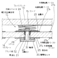
そして、本発明の要部である電圧印加構造部11は、図3に示すように、気密容器10のリアプレート14に設けられた貫通孔21と、この貫通孔21内に挿通されてアノード15に電位を供給する金属ピン22と、この金属ピン22に電気的に接続される金属板23と、この金属板23に電気的に接続される圧縮コイルバネ24と、金属ピン22をフェイスプレート13に接合するための接合材25と、金属ピン22と金属板23を電気的に接続するためのソケット26とを有している。
【0036】
また、貫通孔21の開口端部には、表示部5の背面側に臨むリアプレート14の背面(以下、リアプレート14の外面と称する。)上に、内面側金属ペースト27aが円環状に設けられており、フェイスプレート13に対向するリアプレート14の前面(以下、リアプレート14の内面と称する。)上に、外面側金属ペースト27cが円環状に設けられている。さらに、これら内面側金属ペースト27aおよび外面側金属ペースト27cの外周側には、図2および図3に示すように、外周側金属ペースト27b,27dがそれぞれ設けられている。
【0037】
貫通孔21は、直径が2mm程度に形成されており、その外周部に設けられた各金属ペースト27a、27b、27c、27dは、銀を主成分とするペースト材を印刷した後、360℃で10分間乾燥し、420℃で10分間焼成することによって形成されている。
【0038】
金属ピン22は、貫通穴21に挿通される小径部である軸部31と、この軸部31の基端側に一体に設けられた大径部である略円板状のフランジ部32とを有している。金属ピン22は、例えば、材料として42Ni−6Cr−Fe合金(熱膨張係数7.5〜9.8×10⁻⁶/℃)によって形成することができる。ここでは熱膨張係数9.0×10-6/℃のNi−6Cr−Fe合金からなる金属ピンを用いた。金属ピン22は、軸部31が直径0.5mm程度、フランジ部32が直径5mm程度に形成されている。そして、金属ピン22は、熱膨張を、リアプレート14を形成したガラス材(熱膨張係数9.0×10-6/℃)の熱膨張と略一致させることで、電圧印加構造部11の作製時に生じる熱応力を緩和している。
【0039】
なお、金属ピン22は、材料として、例えば、インバー合金、47Ni−Fe合金(熱膨張係数3.0〜5.5×10⁻⁶/℃)や、42Ni−6Cr−Fe合金(熱膨張係数7.5〜9.8×10-6/℃)など、リアプレート14に使用されるガラス材の熱膨張係数(5.0〜9.0×10-6/℃)に合わせる(熱膨張係数の差の絶対値が3.0×10-6/℃以内になる)ように、熱膨張係数2.0〜12.0×10-6/℃の金属材から適宜選択することが好ましい。
【0040】
さらに、金属ピン22の表面には、接合材25との濡れ性を向上して接合強度を向上するための導電性メッキ35が被覆されている。導電性メッキ35として、例えば、無電解ニッケルメッキを厚さ3μm程度被覆した後に、無電解金メッキを厚さ0.05μm程度で金属ピン22全体に被覆している。なお、導電性メッキ35としては、例えば金、銀、ニッケル、銅などの材料から、接合材25との濡れ性を考慮して選択することが好ましい。
【0041】
そして、金属ピン22は、フランジ部32が、リアプレート14の外面上に、接合材25を介して接合されている。接合材25としては、例えばインジウムを使用している。金属ピン22と金属ペースト27cとの間の1箇所のみを電圧印加構造部11の接合面とすることにより、接合不良による漏電や強度低下が生じる確率を抑えることができる。なお、接合材としては、下地である金属ペースト27cとの濡れ性を考慮して、例えばインジウム、鉛半田、フリットなどの材料から適宜選択することが好ましい。
【0042】
圧縮コイルバネ24は、レーザースポット溶接によって金属板23の主面上に接合されている。圧縮コイルバネ24は、例えば、線径0.2mmのステンレス鋼線によって、自然長7mm、外径4mmをなす形状に形成されている。電圧印加構造部11は、圧縮コイルバネの構造を採用したことにより、バネ長さを短くしても、バネピッチを大きくすることで、比較的大きなストロークを得ることが可能とされて、薄型平面型の表示装置1に特有の比較的狭いエリアにおいても弾性力を安定して機能させることができる。
【0043】
金属板23は、例えば、直径5mm、厚さ0.05mm程度のステンレス板をエッチング処理することにより作製される。この金属板23は、金属ピン22の軸部31が挿通される中心穴(不図示)を有している。ソケット26は、導電性を有する金属材料によって円筒状に形成されており、金属板23の中心穴にソケット26が係合されて設けられている。
【0044】
そして、金属板23は、ソケット26内に金属ピン22の軸部31を嵌め込むことによって位置決めされて、フェイスプレート13の設置後に、溶接されている圧縮コイルバネ24によってリアプレート14側に押し付けられることにより、さらに確実に位置決めされて設置される。
【0045】
以上のように構成された電圧印加構造部11は、電圧が、リアプレート14の外面側から印加され、貫通孔21に軸部31が挿通された金属ピン22を介し、ソケット26、金属板23、圧縮コイルバネ24を通って、アノード15に印加される。
【0046】
そして、表示装置1が備える表示部5には、アノード15に電圧を印加することにより、リアプレート14上のカソードから真空中に放出された電子が加速され、アノード15に設けられた蛍光体(不図示)に衝突し発光させることによって画像等の情報が表示される。
【0047】
上述した電圧印加構造部11は、圧縮コイルバネ24、ソケット26、金属板23と金属ピン22をそれぞれ別体とした導通構造を採用したことにより、金属ピン22のリアプレート14に対する設置位置の精度にかかわらずに圧縮コイルバネ24を設置できるため、圧縮コイルバネ24の弾性力を安定して得ることができる。さらに、圧縮コイルバネ24、ソケット26、金属板23と金属ピン22とを別体に構成したことにより、金属ピン22の設置後に、圧縮コイルバネ24、ソケット26、金属板23を設置することができ、金属ピン22の設置加工時の変形を防止することができる。
【0048】
金属ペースト27cは、接合材25が導電性を有しているため、金属ピン22とほぼ同電位であり、金属ペースト27aは金属ピン22と同電位である金属板23に接触させることによって、金属ピン22とほぼ同電位としている。一方、金属ペースト27b、27dは接地されている。これは、電圧を規定した導電性の金属ペーストで囲み電位基準を決めることによって、電圧印加構造部11全体の電位を安定させるためである。
【0049】
また、電圧印加構造部11は、構造体である金属ピン22、圧縮コイルバネ24が、貫通穴21の外周部の各金属ペースト27a、27b、27c、27dによって包囲されることによって、形状に起因して構造体などの突起状をなす部分に生じ易い電界集中を、端部の形状を滑らかに作製し易い金属ペースト27a、27b、27c、27dで肩代わりさせることで、電界集中に起因して発生する放電を抑制することができる。
【0050】
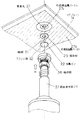
上述した電圧印加構造部11を組み立てる組立方法について図面を参照して説明する。図4に、超音波半田ごてを用いて電圧印加構造部11を組み立てる状態の斜視図を示し、図5に電圧印加構造部11を組み立てる工程を示す。
【0051】
図5(a)に示すように、リアプレート14のカソード(不図示)側の内面上に各金属ペースト27a、27bを印刷によって塗布し、同様に外面上に各金属ペースト27c、27dを印刷によって塗布して、420℃で10分間焼成した。
【0052】
次いで、図4に示すように、超音波半田ごて37の保持部38に金属ピン22のフランジ部32を取り付けて保持させる。図5(b)および図5(c)に示すように、超音波半田ごて37の保持部38によって保持された金属ピン22を、フランジ部32とリアプレート14との間に接合材25を挟み込んで、保持部37を図4中矢印a方向に移動させて、リアプレート14の外面側から貫通孔21内へ金属ピン22の軸部31を挿通して設置する。
【0053】
超音波半田ごて37を加熱することにより、接合材25であるインジウムが溶融する160℃まで昇温する。接合材25が溶融したときに、超音波半田ごて37によって超音波振動を印加するとともに、超音波半田ごて37を移動させて、リアプレート14の貫通孔21内に金属ピン22の軸部31を押し込み、その後接合材25を室温まで冷却する。
【0054】
接合材25が十分に冷却された後、超音波半田ごて37の保持部37を金属ピン22のフランジ部32から取り外す。その後、図4(d)に示すように、リアプレート14の内面側から金属板23と圧縮コイルバネ24を金属ピン22の軸部31に差し込むことによって、電圧印加構造部11が完成する。
【0055】
上述したように、超音波半田ごて37を使用することによって、接合材25、金属ペースト27a、27c、金属ピン22のフランジ部32の接合界面の酸化層を破って拡散接合が行われ、良好な接合が可能となる。また、超音波半田ごて37の保持部37に金属ピン22が保持されることによって、超音波半田ごて37による加熱温度と超音波を十分に接合材25と接合界面に印加することができる。これにより、リアプレート14の貫通孔21に対して金属ピン22を高い気密性で接合することが可能とされて、気密容器10に電圧を良好に印加することができる。
【0056】
上述したように、第1の実施形態の表示装置1によれば、電圧印加構造部11が、金属ピン22、金属板23、圧縮コイルバネ24と、これらの構造体の周囲を囲む各金属ペースト27a、27b、27c、27dとを有し、超音波半田ごて37を用いて作製することにより、貫通孔21を封止する接合界面を1箇所にすることができ、接合不良や漏電の確率を抑えることができる。したがって、この表示装置1によれば、製造時の歩留まりを向上することができ、より廉価な表示装置を提供することができる。
【0057】
(第2の実施形態)
つぎに、他の電圧印加構造部を備える第2の実施形態の表示装置を説明する。この第2の実施形態の表示装置は、上述した第1の実施形態の表示装置1と電圧印加構造部の一部を除く基本的な構成が同一であるため、同一部材には同一符号を付して説明を省略する。図6に電圧印加構造部の縦断面図を示す。
【0058】
図6に示すように、第2の実施形態の表示装置2が備える電圧印加構造部51は、リアプレート14の貫通孔21内に挿通されてアノード15に電位を供給するためのガラスピン53と、このガラスピン53に電気的に接続される金属板55と、この金属板55に電気的に接続される圧縮コイルバネ54とを有している。
【0059】
ガラスピン53は、貫通穴21に挿通される小径部である軸部56と、この軸部56の基端側に一体に設けられた大径部である略円板状のフランジ部57とを有している。ガラスピン53は、例えば、材料としてPD200(旭硝子株式会社製)によって、軸部56が直径1.5mm程度、フランジ部57が直径5mm程度に形成されている。そして、ガラスピン53は、熱膨張を、リアプレート14を形成したガラス材(熱膨張係数8.0〜9.0×10⁻⁶/℃)の熱膨張と略一致させることで、電圧印加構造部11の作製時に生じる熱応力を緩和している。
【0060】
また、ガラスピン53の表面には、接合材25との濡れ性を向上して接合強度を向上するための導電性メッキ58が被覆されている。導電性メッキ58として、例えば、無電解ニッケルメッキを厚さ3μm程度被覆した後に、無電解金メッキを厚さ0.05μm程度でガラスピン53全体に被覆している。
【0061】
そして、ガラスピン53は、フランジ部57が、リアプレート14の外面上に、接合材25を介して接合されている。接合材25としては、フリットを使用している。電圧印加構造部51は、ガラスピン53と金属ペースト27cとの間の1箇所のみを接合面とすることにより、接合不良による漏電や強度低下が生じる確率を抑えることができる。
【0062】
圧縮コイルバネ54は、一端がレーザースポット溶接によってガラスピン53の軸部71の先端に接合されている。圧縮コイルバネ54は、例えば、線径0.2mmのピアノ線によって、自然長2mm、外径1.2mmをなす形状に形成されている。電圧印加構造部51は、圧縮コイルバネの構造を採用したことにより、バネ長さを短くしても、バネピッチを大きくすることで、比較的大きなストロークを得ることが可能とされて、薄型平面型の表示装置1に特有の比較的狭いエリアにおいても弾性力を安定して機能させることができる。
【0063】
上述したように、ガラスピン53と圧縮コイルバネ54を一体的に構成したことによって、ガラスピン53と圧縮コイルバネ54との接触不良によるアノード15への導通不良が発生することを抑えられる。
【0064】
金属板55は、例えば、直径6mm、厚さ0.05mm程度のステンレス板をエッチング処理することにより作製される。この金属板55は、プレス加工によって外周部が反らされており、内面側金属ペースト27aとの接触が良好に確保されている。また、この金属板55は、ガラスピン53の軸部56が挿通される中心穴(不図示)を有しており、この中心穴にソケット26が係合されている。
【0065】
以上のように構成された電圧印加構造部51は、電圧が、リアプレート14の外面側から印加され、貫通孔21に軸部31が挿通されたガラスピン53を介し、ソケット26、金属板55、圧縮コイルバネ54を通って、アノード15に印加される。
【0066】
そして、表示装置2が備える表示部には、アノード15に電圧を印加することにより、リアプレート14上のカソードから真空中に放出された電子が加速され、アノード15に設けられた蛍光体に衝突し発光させることによって画像等の情報が表示される。
【0067】
上述した電圧印加構造部51は、接合材25が導電性を有しているため、金属ペースト27cがガラスピン53とほぼ同電位であり、金属ペースト27aがガラスピン53と同電位である金属板55に接触させることによって、ガラスピン53とほぼ同電位としている。一方、金属ペースト27b、27dは接地されている。これは、電圧を規定した導電性の金属ペーストで囲み電位基準を決めることによって、電圧印加構造部51全体の電位を安定させるためである。
【0068】
また、電圧印加構造部51は、構造体であるガラスピン53、圧縮コイルバネ54が、貫通穴21の外周部の各金属ペースト27a、27b、27c、27dによって包囲されることによって、形状に起因して構造体などの突起状をなす部分に生じ易い電界集中を、端部の形状を滑らかに作製し易い金属ペースト27a、27b、27c、27dで肩代わりさせることで、電界集中に起因して発生する放電を抑制することができる。
【0069】
上述した電圧印加構造部51を接合材25としてフリットを用いて組み立てる組立方法を説明する。
【0070】
リアプレート14のカソード側の内面上に各金属ペースト27a、27bを印刷によって塗布し、同様に外面上に各金属ペースト27c、27dを印刷によって塗布して、420℃で10分間焼成した。
【0071】
次いで、超音波半田ごて37の保持部38にガラスピン53のフランジ部57を取り付けて保持させる。超音波半田ごて37の保持部38によって保持されたガラスピン53を、フランジ部57とリアプレート14との間に接合材25を挟み込んで、保持部37を矢印a方向に移動させて、リアプレート14の外面側から貫通孔21内へガラスピン53の軸部56を挿通して設置する。
【0072】
超音波半田ごて37を加熱することにより、接合材25であるフリットが溶融する420℃まで昇温する。ここで、超音波半田ごて37による局所的な加熱であるときにリアプレート14が熱割れし易くなるが、リアプレート14全体をホットプレート(不図示)により350℃付近まで昇温させることで熱割れの発生を抑えることができる。
【0073】
そして、接合材25が溶融したときに、超音波半田ごて37によって超音波振動を印加するとともに、超音波半田ごて37を移動させて、リアプレート14の貫通孔21内にガラスピン53の軸部56を押し込み、その後接合材25を室温まで冷却する。
【0074】
接合材25が十分に冷却された後、超音波半田ごて37の保持部37をガラスピン53のフランジ部57から取り外す。その後、リアプレート14の内面側から金属板55と圧縮コイルバネ54をガラスピン53の軸部56に差し込むことによって、電圧印加構造部51が完成する。
【0075】
上述したように、超音波半田ごて37を使用することによって、接合材25、金属ペースト27a、27c、ガラスピン53のフランジ部57の接合界面の酸化層を破って拡散接合が行われ、良好な接合が可能となる。また、超音波半田ごて37の保持部37にガラスピン53が保持されることによって、超音波半田ごて37による加熱温度と超音波を十分に接合材25と接合界面に印加することができる。これにより、リアプレート14の貫通孔21に対してガラスピン53を高い気密性で接合することが可能とされて、気密容器に電圧を良好に印加することができる。
【0076】
上述したように、第2の実施形態の表示装置2によれば、電圧印加構造部51が、ガラスピン53、金属板55、圧縮コイルバネ54と、これらの構造体の周囲を囲む各金属ペースト27a、27b、27c、27dとを有し、超音波半田ごて37を用いて作製することにより、貫通孔21を封止する接合界面を1箇所にすることができ、接合不良や漏電の確率を抑えることができる。したがって、この表示装置2によれば、製造時の歩留まりを向上することができ、より廉価な表示装置を提供することができる。
【0077】
(第3の実施形態)
最後に、更に他の電圧印加構造部を備える第3の実施形態の表示装置について説明する。この第3の実施形態の表示装置は、上述した第1の実施形態の表示装置と電圧印加構造部を除く基本構成が同一であるため、同一部材には同一符号を付して説明を省略する。図7に電圧印加構造部の縦断面図を示す。
【0078】
第3の実施形態の表示装置3が備える電圧印加構造部61は、図7に示すように、リアプレート14の貫通孔21内に挿入されてアノード15に電位を供給する金属ピン63と、この金属ピン63に電気的に接続される金属板64と、この金属板64に電気的に接続される圧縮コイルバネ65とを有している。
【0079】
金属ピン63は、貫通穴21に挿入される小径部である軸部71と、この軸部71の基端側に一体に設けられた大径部である略円板状のフランジ部72とを有している。金属ピン63は、例えば、材料として47Ni−Fe合金(熱膨張係数3.0〜5.5×10⁻⁶/℃)を用いればよく、ここでは熱膨張係数5.5×10-6/℃の47Ni−Fe合金からなる金属ピンとした。軸部71が直径1.5mm程度、フランジ部72が直径5mm程度に形成されている。そして、リアプレート14を構成するガラス材としては熱膨張係数が8.0×10-6/℃のものを用いたので、金属ピン63の熱膨張係数と、リアプレート14を形成したガラス材の熱膨張係数との差が2.5×10-6/℃となり、3.0×10-6/℃以内であるため、電圧印加構造部61の作製時に生じる熱応力が抑制されている。
【0080】
また、金属ピン63の軸部71には、金属板64の一部が係合される係合孔74が、軸部71の先端側から軸方向と平行に加工されている。この係合孔74は、孔径0.6mm程度に形成されており、軸部71の中心部で、孔径が1.5倍に拡径されて加工されている。
【0081】
さらに、金属ピン63の表面には、接合材25との濡れ性を向上して接合強度を向上するための導電性メッキ73が被覆されている。導電性メッキ73として、例えば、無電解ニッケルメッキを厚さ3μm程度被覆した後に、無電解銀メッキを厚さ0.05μm程度で、係合孔74内を除く金属ピン63全体に被覆している。
【0082】
そして、金属ピン63は、フランジ部72が、リアプレート14の外面上に、接合材25を介して接合されている。接合材25としては、例えば鉛半田を使用している。電圧印加構造部61は、金属ピン63と金属ペースト27cとの間の1箇所のみを接合面とすることにより、接合不良による漏電や強度低下が生じる確率を抑えることができる。
【0083】
圧縮コイルバネ65は、レーザースポット溶接によって金属板64の主面上に接合されている。圧縮コイルバネ65は、例えば、線径0.2mmのステンレス鋼線によって、自然長7mm、外径4mmをなす形状に形成されている。電圧印加構造部61は、圧縮コイルバネの構造を採用したことにより、バネ長さを短くしても、バネピッチを大きくすることで、比較的大きなストロークを得ることが可能とされて、薄型平面型の表示装置3に特有の比較的狭いエリアにおいても弾性力を安定して機能させることができる。
【0084】
金属板64は、例えば、直径5mm、厚さ0.05mm程度のステンレス板をエッチング処理することにより作製される。この金属板64の主面の中央部には、金属ピン63の軸部71の係合孔74に係合されるフック68が一体に設けられている。このフック68は、例えば、線径0.2mm程度のステンレス鋼線によって形成されており、金属板64の主面の中央部に溶接されて接合されている。また、フック68は、例えば金属板64の主面の一部を切り起こして形成されてもよい。フック68は、金属板64の係合孔74に係合されることにより、金属ピン63と金属板64の導通を確保している。
【0085】
そして、金属板64は、金属ピン63の軸部71の係合孔74にフック68を係合させることによって位置決めされて、フェイスプレート13の設置後に、溶接されている圧縮コイルバネ65によってリアプレート14側に押し付けられることにより、さらに確実に位置決めされて設置される。
【0086】
以上のように構成された電圧印加構造部61は、電圧が、リアプレート14の外面側から印加され、貫通孔21に軸部71が挿入された金属ピン63を介し、フック68、金属板64、圧縮コイルバネ65を通って、アノード15に印加される。
【0087】
そして、表示装置1が備える表示部には、アノード15に電圧を印加することにより、リアプレート14上のカソードから真空中に放出された電子が加速され、アノード15に設けられた蛍光体に衝突し発光させることによって画像等の情報が表示される。
【0088】
上述した電圧印加構造部61は、圧縮コイルバネ65、フック68、金属板64と金属ピン63をそれぞれ別体とした導通構造を採用したことにより、金属ピン63のリアプレート14に対する設置位置の精度にかかわらずに圧縮コイルバネ65を設置できるため、圧縮コイルバネ65の弾性力を安定して得ることができる。さらに、圧縮コイルバネ65、フック68、金属板64と金属ピン63とを別体に構成したことにより、金属ピン63の設置後に、圧縮コイルバネ65、金属板64を設置することができ、金属ピン63の設置加工時の変形を防止することができる。
【0089】
金属ペースト27cは、接合材25が導電性を有しているため、金属ピン63とほぼ同電位であり、金属ペースト27aは金属ピン63と同電位である金属板64に接触させることによって、金属ピン63とほぼ同電位としている。一方、金属ペースト27b、27dは接地されている。これは、電圧を規定した導電性の金属ペーストで囲み電位基準を決めることによって、電圧印加構造部61全体の電位を安定させるためである。
【0090】
また、電圧印加構造部61は、構造体である金属ピン63、圧縮コイルバネ65が、貫通穴21の外周部の各金属ペースト27a、27b、27c、27dによって包囲されることによって、形状に起因して構造体などの突起状をなす部分に生じ易い電界集中を、端部の形状を滑らかに作製し易い金属ペースト27a、27b、27c、27dで肩代わりさせることで、電界集中に起因して発生する放電を抑制することができる。
【0091】
上述した電圧印加構造部61を接合材25として鉛半田を用いて組み立てる組立方法を説明する。
【0092】
リアプレート14のカソード側の内面上に各金属ペースト27a、27bを印刷によって塗布し、同様に外面上に各金属ペースト27c、27dを印刷によって塗布して、420℃で10分間焼成した。
【0093】
次いで、超音波半田ごて37の保持部38に金属ピン63のフランジ部72を取り付けて保持させる。超音波半田ごて37の保持部38によって保持された金属ピン63を、フランジ部72とリアプレート14との間に接合材25を挟み込んで、保持部37を矢印a方向に移動させて、リアプレート14の外面側から貫通孔21内へ金属ピン63の軸部71を挿入して設置する。
【0094】
超音波半田ごて37を加熱することにより、接合材25である鉛半田が溶融する160℃まで昇温する。接合材25が溶融したときに、超音波半田ごて37によって超音波振動を印加するとともに、超音波半田ごて37を移動させて、リアプレート14の貫通孔21内に金属ピン63の軸部71を押し込み、その後接合材25を室温まで冷却する。
【0095】
接合材25が十分に冷却された後、超音波半田ごて37の保持部37を金属ピン63のフランジ部72から取り外す。その後、リアプレート14の内面側から金属板64と圧縮コイルバネ65を金属ピン63の軸部71に差し込むことによって、電圧印加構造部61が完成する。
【0096】
上述したように、超音波半田ごて37を使用することによって、接合材25、金属ペースト27a、27c、金属ピン63のフランジ部72の接合界面の酸化層を破って拡散接合が行われ、良好な接合が可能となる。また、超音波半田ごて37の保持部37に金属ピン63が保持されることによって、超音波半田ごて37による加熱温度と超音波を十分に接合材25と接合界面に印加することができる。これにより、リアプレート14の貫通孔21に対して金属ピン63を高い気密性で接合することが可能とされて、気密容器10に電圧を良好に印加することができる。
【0097】
上述したように、第3の実施形態の表示装置3によれば、電圧印加構造部61が、金属ピン63、金属板64、圧縮コイルバネ65と、これらの構造体の周囲を囲む各金属ペースト27a、27b、27c、27dとを有し、超音波半田ごて37を用いて作製することにより、貫通孔21を封止する接合界面を1箇所にすることができ、接合不良や漏電の確率を抑えることができる。したがって、この表示装置1によれば、製造時の歩留まりを向上することができ、より廉価な表示装置を提供することができる。
【0098】
なお、本実施形態に係る表示装置が備える各電圧印加構造部は、圧縮コイルバネを有する構成とされたが、例えば、板バネ等の他のバネや、導電性を有する弾性材料等を有する構成とされてもよいことは勿論である。
【0099】
【発明の効果】
上述したように本発明によれば、第1の導電性部材の第2の部分と貫通孔との接合不良や、電極の電位に漏電が発生することを抑制することができる。したがって、本発明によれば、気密容器の製造時に気密容器の歩留まりを向上することを可能とし、より廉価な表示装置、気密容器およびこの気密容器の製造方法を提供することができる。
【図面の簡単な説明】
【図1】本発明に係る第1の実施形態の表示装置を示す斜視図である。
【図2】前記表示装置が備える気密容器を背面側から示す背面図である。
【図3】図1の電圧印加構造部を示すA−A断面図である。
【図4】超音波半田ごてを用いて電圧印加構造部を組み立てる状態を示す斜視図である。
【図5】前記電圧印加構造部を組み立てる工程を説明するために示す縦断面図である。
【図6】本発明に係る第2の実施形態の表示装置が備える気密容器の要部を示す縦断面図である。
【図7】本発明に係る第3の実施形態の表示装置が備える気密容器の要部を示す縦断面図である。
【図8】従来の表示装置の要部を示す斜視図である。
【符号の説明】
1 表示装置
2 表示装置
3 表示装置
5 表示部
10 気密容器
11 電圧印加構造部
13 フェイスプレート
14 リアプレート
15 アノード
16 枠
21 貫通孔
22 金属ピン
23 金属板
24 圧縮コイルバネ
25 接合材
26 ソケット
27a 内面側金属ペースト
27b 外面側金属ペースト
27c,27d 外周側金属ペースト
31 軸部
32 フランジ部
35 導電性メッキ
37 超音波半田ごて
51 電圧印加構造部
53 ガラスピン
54 圧縮コイルバネ
55 金属板
56 軸部
57 フランジ部
58 導電性メッキ
61 電圧印加構造部
63 金属ピン
64 金属板
65 圧縮コイルバネ
68 フック
71 軸部
72 フランジ部
73 導電性メッキ
74 係合溝
101 表示装置
106 前面パネル
107 背面パネル
108 給電導電層
109 カソード
114 蛍光面電位給電用端子
115 弾性体
116 孔部
117 端子導出部
120 蛍光面[0001]
BACKGROUND OF THE INVENTION
The present invention relates to a display device such as a television receiver or a computer that displays information such as characters and images, and a message board that displays characters..
[0002]
[Prior art]
In recent years, a color cathode ray tube (CRT) has been widely used as a display device. However, the driving principle is a method of deflecting an electron beam emitted from a cathode and causing a phosphor of the screen to emit light. It was necessary to secure depth. In general, the display device becomes longer in depth as the screen size is increased. For this reason, as a display device, a flat display device that is thin and can be reduced in weight is strongly desired because of problems such as an increase in installation space and an increase in weight.
[0003]
As a conventional flat display device, for example, a surface conduction electron emission display device (hereinafter referred to as SED) as disclosed in Japanese Patent Application Laid-Open No. 09-045266, or Japanese Patent Application Laid-Open No. 05-114372. A field emission type display device (hereinafter referred to as FED) as disclosed in the publication is known.
[0004]
FIG. 8 shows a perspective view of the FED (Japanese Patent Laid-Open No. 05-114372). The FED will be briefly described with reference to the drawings.
[0005]
The FED 101 includes an airtight container as a display unit that displays information such as an image. As shown in FIG. 8, in this hermetic container, insulating layers 111 and 112 are sandwiched between a
[0006]
In addition, the hermetic container is provided with a hole 116 through which a fluorescent screen potential power supply terminal 114 having an elastic body 115 at the tip is inserted in the
[0007]
The FED 101 having the hermetic container configured as described above emits electrons from the
[0008]
[Problems to be solved by the invention]
As described above, the hermetic container included in the conventional display device is hermetically sealed with a sealing member such as a sealing body in order to maintain the inside in a vacuum state. It was necessary to cover and seal.
[0009]
That is, one of the problems to be solved by the present invention is to suitably realize a configuration for supplying a potential to an electrode provided inside an airtight container. In particular, an object is to realize a configuration in which an airtight container can easily maintain airtightness. Another object is to realize a configuration in which the potential of the opening end portion of the through hole for supplying the potential to the inside can be easily defined.
[0010]
[Means for Solving the Problems]
One aspect of the present invention is configured as follows. That is, the display device according to the present invention includes a cathode that emits electrons and an electrode to which a potential is applied from the outside., ElectricThe pole is placedTheWith the first substrateThe secondIt is provided to face one substrate with a gap, With a through holeA second substrateThe secondFirst conductive member for supplying a potential to the electrode from the outer surface side of the second substrate through the second substrateA first portion located in the through hole and a second portion provided integrally with the first portion and located at the opening end of the through hole, the second portion being A first conductive member sealed airtightly on the outer surface of the second substrateAnd withHaveThe AndA second conductive member is provided on the inner surface of the second substrate, provided at the opening end of the through hole, and electrically connected to the first conductive member.ing.
[0011]
In the display device configured as described above, the configuration in which the first portion and the second portion of the first conductive member are provided integrally is the first portion of the first conductive member and the first portion of the first conductive member. And a pressure difference between the pressure in the space between the first substrate and the second substrate and the pressure on the outer surface side of the second substrate is loaded. The structure does not have a coupling part. That is, when the first part and the second part are provided separately, and are configured by connecting these parts, and the above-described pressure difference is applied to the combined part. It is necessary to ensure sufficient airtightness of the joined portions. However, according to the present invention, since the first conductive member does not have a coupling portion in the portion where the pressure difference is loaded, the hermeticity breakage in the first conductive member itself is suppressed. can do.
[0014]
In addition, the display device according to the present invention is provided between the first conductive member and the electrode.Set inKeraThe second1 Conductive member and electrodeEachEquipped with electrically conductive and easily deformable membersHaveIt is preferable. According to this configuration, even if there is an error in the distance between the first substrate and the second substrate due to the deformation of the conductive easily deformable member, the electrical conductivity between the first conductive member and the electrode is Connection can be ensured. As the conductive easily deformable member, a spring, particularly preferably a compression coil spring can be used. However, the conductive easily deformable member is not limited to the spring, and any member that can be deformed according to the distance between the substrates when the first substrate and the second substrate are assembled.
[0015]
First1 has a thermal expansion coefficient of 2.0 × 10⁻⁶/ ℃ or more,12.0 × 10-6A configuration comprising a base material at a temperature of / ° C. or less can be suitably employed, and the absolute value of the difference from the thermal expansion coefficient of the second substrate within the range is 3.0 × 10⁻⁶/ ° C or less is preferred. As the substrate, metals (including alloys) and glass can be employed. Moreover, you may use what formed the film | membrane on the surface of the base material as a 1st electroconductive member. When the substrate is an insulator, conductivity can be imparted by using a conductive film such as conductive plating as the surface film.
[0016]
In addition, the second portion of the first conductive member included in the display device according to the present invention improves the wettability with the bonding material to the bonding portion bonded to the second substrate via the bonding material. A membrane is preferably provided. As the film for improving the wettability, for example, plating may be employed, and it is particularly preferable to employ gold plating.
[0017]
In the display device according to the present invention, the bonding material is preferably made of a metal material. The metal material may be an alloy. Moreover, you may use low melting glass as things other than a metal material, for example.
[0018]
In the display device according to the present invention, a potential for accelerating electrons emitted from the cathode is supplied to the electrode.
[0027]
In the present invention, the inner surface of the second substrate refers to the front surface facing the first substrate, and the outer surface of the second substrate refers to the rear surface facing the back side of the display device. is there.
[0029]
DETAILED DESCRIPTION OF THE INVENTION
Hereinafter, a specific embodiment of the present invention will be described with reference to the drawings for a thin flat display device.
[0030]
(First embodiment)
As shown in FIG. 1, the display device 1 includes a display unit 5 that displays various information such as characters and images. Further, the display device 1 covers a control unit (not shown) that drives and controls the display unit 5, a support frame (not shown) that supports the display unit 5 and the control unit, and the display unit 5, the control unit, and the support frame. And a cover 8 which is an outer casing.
[0031]
As shown in FIGS. 2 and 3, the display unit 5 includes an
[0032]
As shown in FIG. 2, the
[0033]
The
[0034]
The
[0035]
And the voltage application structure part 11 which is the principal part of this invention is inserted in the through-hole 21 provided in the
[0036]
Further, an inner surface
[0037]
The through-hole 21 is formed to have a diameter of about 2 mm, and the metal pastes 27a, 27b, 27c, and 27d provided on the outer periphery of the through-hole 21 are printed at 360 ° C. after printing a paste material mainly composed of silver. It is formed by drying for 10 minutes and baking at 420 ° C. for 10 minutes.
[0038]
The
[0039]
The
[0040]
Furthermore, the surface of the
[0041]
The
[0042]
The compression coil spring 24 is joined to the main surface of the metal plate 23 by laser spot welding. The compression coil spring 24 is formed of, for example, a stainless steel wire having a wire diameter of 0.2 mm and having a natural length of 7 mm and an outer diameter of 4 mm. By adopting a compression coil spring structure, the voltage application structure section 11 can obtain a relatively large stroke by increasing the spring pitch even if the spring length is shortened. Even in a relatively narrow area peculiar to the display device 1, the elastic force can be stably functioned.
[0043]
The metal plate 23 is produced, for example, by etching a stainless plate having a diameter of about 5 mm and a thickness of about 0.05 mm. The metal plate 23 has a center hole (not shown) through which the
[0044]
Then, the metal plate 23 is positioned by fitting the
[0045]
In the voltage application structure portion 11 configured as described above, a voltage is applied from the outer surface side of the
[0046]
In the display unit 5 provided in the display device 1, by applying a voltage to the anode 15, electrons emitted from the cathode on the
[0047]
The voltage application structure 11 described above employs a conduction structure in which the compression coil spring 24, the
[0048]
Since the
[0049]
In addition, the voltage application structure portion 11 is caused by the shape of the
[0050]
An assembly method for assembling the above-described voltage application structure 11 will be described with reference to the drawings. FIG. 4 shows a perspective view of a state where the voltage application structure 11 is assembled using an ultrasonic soldering iron, and FIG. 5 shows a process of assembling the voltage application structure 11.
[0051]
As shown in FIG. 5A, the metal pastes 27a and 27b are applied by printing on the inner surface of the
[0052]
Next, as shown in FIG. 4, the
[0053]
By heating the
[0054]
After the
[0055]
As described above, by using the
[0056]
As described above, according to the display device 1 of the first embodiment, the voltage application structure 11 includes the metal pins 22, the metal plate 23, the compression coil spring 24, and the metal pastes 27a surrounding the structures. 27b, 27c, and 27d, and using the
[0057]
(Second Embodiment)
Next, a display device according to a second embodiment including another voltage application structure unit will be described. The display device according to the second embodiment has the same basic configuration as the display device 1 according to the first embodiment described above except for a part of the voltage application structure portion. Therefore, the description is omitted. FIG. 6 shows a longitudinal sectional view of the voltage application structure.
[0058]
As shown in FIG. 6, the voltage application structure 51 included in the display device 2 of the second embodiment includes a
[0059]
The
[0060]
The surface of the
[0061]
The
[0062]
One end of the compression coil spring 54 is joined to the tip of the shaft portion 71 of the
[0063]
As described above, by integrally configuring the
[0064]
The
[0065]
In the voltage application structure 51 configured as described above, a voltage is applied from the outer surface side of the
[0066]
In the display unit of the display device 2, by applying a voltage to the anode 15, electrons emitted from the cathode on the
[0067]
In the voltage application structure 51 described above, since the
[0068]
In addition, the voltage application structure 51 is caused by the shape by the
[0069]
An assembly method for assembling the voltage application structure 51 described above using the frit as the
[0070]
The metal pastes 27a and 27b were applied by printing on the inner surface of the
[0071]
Next, the
[0072]
By heating the
[0073]
When the
[0074]
After the
[0075]
As described above, by using the
[0076]
As described above, according to the display device 2 of the second embodiment, the voltage application structure 51 includes the
[0077]
(Third embodiment)
Finally, a display device according to a third embodiment including another voltage application structure will be described. The display device according to the third embodiment has the same basic configuration as the display device according to the first embodiment except for the voltage application structure, and therefore the same members are denoted by the same reference numerals and description thereof is omitted. . FIG. 7 shows a longitudinal sectional view of the voltage application structure.
[0078]
As shown in FIG. 7, the
[0079]
The metal pin 63 includes a shaft portion 71 that is a small-diameter portion that is inserted into the through hole 21, and a substantially disc-shaped flange portion 72 that is a large-diameter portion integrally provided on the proximal end side of the shaft portion 71. Have. The metal pin 63 is made of, for example, 47Ni—Fe alloy (thermal expansion coefficient: 3.0 to 5.5 × 10⁻⁶/ ° C.), and here the thermal expansion coefficient is 5.5 × 10⁻⁶A metal pin made of a 47Ni-Fe alloy at / ° C. The shaft portion 71 is formed with a diameter of about 1.5 mm, and the flange portion 72 is formed with a diameter of about 5 mm. And as a glass material which comprises the
[0080]
In addition, an engagement hole 74 into which a part of the metal plate 64 is engaged is processed in the shaft portion 71 of the metal pin 63 from the distal end side of the shaft portion 71 in parallel with the axial direction. The engagement hole 74 is formed to have a hole diameter of about 0.6 mm, and is processed with the hole diameter being increased by 1.5 times at the center of the shaft portion 71.
[0081]
Further, the surface of the metal pin 63 is covered with a conductive plating 73 for improving the wettability with the
[0082]
The metal pin 63 has the flange portion 72 bonded to the outer surface of the
[0083]
The compression coil spring 65 is joined to the main surface of the metal plate 64 by laser spot welding. The compression coil spring 65 is formed of, for example, a stainless steel wire having a wire diameter of 0.2 mm and having a natural length of 7 mm and an outer diameter of 4 mm. The
[0084]
The metal plate 64 is produced, for example, by etching a stainless plate having a diameter of about 5 mm and a thickness of about 0.05 mm. A hook 68 that is engaged with the engagement hole 74 of the shaft portion 71 of the metal pin 63 is integrally provided at the center of the main surface of the metal plate 64. The hook 68 is formed of, for example, a stainless steel wire having a wire diameter of about 0.2 mm, and is welded and joined to the central portion of the main surface of the metal plate 64. Further, the hook 68 may be formed by cutting and raising a part of the main surface of the metal plate 64, for example. The hook 68 ensures engagement between the metal pin 63 and the metal plate 64 by being engaged with the engagement hole 74 of the metal plate 64.
[0085]
The metal plate 64 is positioned by engaging the hook 68 with the engagement hole 74 of the shaft portion 71 of the metal pin 63, and after the
[0086]
In the
[0087]
In the display unit of the display device 1, by applying a voltage to the anode 15, electrons emitted from the cathode on the
[0088]
The
[0089]
Since the
[0090]
In addition, the voltage
[0091]
An assembly method for assembling the
[0092]
The metal pastes 27a and 27b were applied by printing on the inner surface of the
[0093]
Next, the flange portion 72 of the metal pin 63 is attached to and held by the holding portion 38 of the
[0094]
By heating the
[0095]
After the
[0096]
As described above, by using the
[0097]
As described above, according to the display device 3 of the third embodiment, the
[0098]
In addition, each voltage application structure part with which the display apparatus which concerns on this embodiment is provided was set as the structure which has a compression coil spring, For example, the structure which has other springs, such as a leaf | plate spring, the elastic material which has electroconductivity, etc. Of course, it may be done.
[0099]
【The invention's effect】
As described above, according to the present invention, it is possible to suppress poor bonding between the second portion of the first conductive member and the through hole, and the occurrence of leakage in the electrode potential. Therefore, according to the present invention, it is possible to improve the yield of the hermetic container at the time of manufacturing the hermetic container, and it is possible to provide a more inexpensive display device, hermetic container, and method for manufacturing the hermetic container.
[Brief description of the drawings]
FIG. 1 is a perspective view showing a display device according to a first embodiment of the present invention.
FIG. 2 is a rear view showing an airtight container provided in the display device from the rear side.
3 is a cross-sectional view taken along line AA showing the voltage application structure of FIG. 1. FIG.
FIG. 4 is a perspective view showing a state in which a voltage application structure is assembled using an ultrasonic soldering iron.
FIG. 5 is a longitudinal sectional view for explaining a process of assembling the voltage application structure.
FIG. 6 is a longitudinal sectional view showing a main part of an airtight container provided in a display device according to a second embodiment of the present invention.
FIG. 7 is a longitudinal sectional view showing a main part of an airtight container provided in a display device according to a third embodiment of the present invention.
FIG. 8 is a perspective view showing a main part of a conventional display device.
[Explanation of symbols]
1 Display device
2 display devices
3 Display device
5 display section
10 Airtight container
11 Voltage application structure
13 Face plate
14 Rear plate
15 Anode
16 frames
21 Through hole
22 Metal Pin
23 Metal plate
24 Compression coil spring
25 Bonding material
26 Socket
27a Inner side metal paste
27b External metal paste
27c, 27d outer peripheral side metal paste
31 Shaft
32 Flange
35 Conductive plating
37 Ultrasonic soldering iron
51 Voltage application structure
53 Glass Pin
54 Compression coil spring
55 Metal plate
56 Shaft
57 Flange
58 Conductive plating
61 Voltage application structure
63 Metal pin
64 metal plate
65 Compression coil spring
68 hooks
71 Shaft
72 Flange
73 Conductive plating
74 Engagement groove
101 Display device
106 Front panel
107 Rear panel
108 Feeding conductive layer
109 cathode
114 Phosphor screen potential power supply terminal
115 Elastic body
116 hole
117 Terminal lead-out part
120 phosphor screen
Claims (6)
外部から電位が与えられる電極と、
前記電極が配置された第1の基板と、
前記第1の基板に間隔をあけて対向して設けられ、貫通孔を有する第2の基板と、
前記第2の基板の外面側から該第2の基板を通して前記電極に電位を供給するための第1の導電性部材であって、前記貫通孔内に位置する第1の部分と、該第1の部分と一体に設けられて前記貫通孔の開口端部に位置する第2の部分とを有し、該第2の部分が、該貫通孔を気密に閉塞して該第2の基板の外面上に接合された第1の導電性部材と、
を備える表示装置において、
前記第2の基板の内面上であって、前記貫通孔の開口端部に設けられ、前記第1の導電性部材と電気的に接続された第2の導電性部材を備えることを特徴とする表示装置。A cathode that emits electrons;
An electrode to which a potential is applied from the outside ;
A first substrate on which the electrodes are disposed;
A second substrate having a through hole provided opposite to the first substrate and having a through hole ;
A first conductive member for supplying a potential to the electrode from the outer surface side of the second substrate through the second substrate, the first portion located in the through hole; And a second portion located at the opening end portion of the through hole, and the second portion hermetically closes the through hole, and the outer surface of the second substrate. A first conductive member bonded on top ;
In Ru display device comprising a,
A second conductive member is provided on the inner surface of the second substrate and provided at an opening end of the through hole, and is electrically connected to the first conductive member. Display device.
Priority Applications (6)
| Application Number | Priority Date | Filing Date | Title |
|---|---|---|---|
| JP2002023555A JP3768889B2 (en) | 2002-01-31 | 2002-01-31 | Display device |
| US10/351,482 US6858980B2 (en) | 2002-01-31 | 2003-01-27 | Display device, hermetic container, and method for manufacturing hermetic container |
| KR10-2003-0005457A KR100516606B1 (en) | 2002-01-31 | 2003-01-28 | Display device, hermetic container, and method for manufacturing hermetic container |
| CNB031023207A CN1229848C (en) | 2002-01-31 | 2003-01-30 | Display device, air tight container and method for making air tight container |
| US10/934,491 US6967434B2 (en) | 2002-01-31 | 2004-09-07 | Display device, hermetic container, and method for manufacturing hermetic container |
| US11/242,845 US7154216B2 (en) | 2002-01-31 | 2005-10-05 | Display device, hermetic container, and method for manufacturing hermetic container |
Applications Claiming Priority (1)
| Application Number | Priority Date | Filing Date | Title |
|---|---|---|---|
| JP2002023555A JP3768889B2 (en) | 2002-01-31 | 2002-01-31 | Display device |
Related Child Applications (1)
| Application Number | Title | Priority Date | Filing Date |
|---|---|---|---|
| JP2005370156A Division JP4056073B2 (en) | 2005-12-22 | 2005-12-22 | Display device |
Publications (3)
| Publication Number | Publication Date |
|---|---|
| JP2003229080A JP2003229080A (en) | 2003-08-15 |
| JP2003229080A5 JP2003229080A5 (en) | 2005-11-04 |
| JP3768889B2 true JP3768889B2 (en) | 2006-04-19 |
Family
ID=27606401
Family Applications (1)
| Application Number | Title | Priority Date | Filing Date |
|---|---|---|---|
| JP2002023555A Expired - Fee Related JP3768889B2 (en) | 2002-01-31 | 2002-01-31 | Display device |
Country Status (4)
| Country | Link |
|---|---|
| US (3) | US6858980B2 (en) |
| JP (1) | JP3768889B2 (en) |
| KR (1) | KR100516606B1 (en) |
| CN (1) | CN1229848C (en) |
Families Citing this family (20)
| Publication number | Priority date | Publication date | Assignee | Title |
|---|---|---|---|---|
| JP3684216B2 (en) * | 2001-07-31 | 2005-08-17 | キヤノン株式会社 | Display device |
| US7861169B2 (en) * | 2001-11-19 | 2010-12-28 | Ricoh Co. Ltd. | Multimedia print driver dialog interfaces |
| JP3950829B2 (en) * | 2002-08-28 | 2007-08-01 | キヤノン株式会社 | Airtight container and image display device manufacturing method |
| JP3940841B2 (en) * | 2002-12-27 | 2007-07-04 | キヤノン株式会社 | Display device |
| KR100563048B1 (en) * | 2003-09-25 | 2006-03-24 | 삼성에스디아이 주식회사 | Plasma display panel assembly |
| JP4250608B2 (en) * | 2004-04-09 | 2009-04-08 | キヤノン株式会社 | Image display device and manufacturing method thereof |
| CN100407361C (en) * | 2004-05-21 | 2008-07-30 | 东元奈米应材股份有限公司 | Construction of field emission display having reflection layer and grid |
| US7102279B2 (en) * | 2004-06-30 | 2006-09-05 | Teco Nanotech Co., Ltd. | FED with insulating supporting device having reflection layer |
| CN101238244B (en) * | 2005-01-24 | 2011-03-30 | 株式会社昭和 | Process for producing crystalline titanium oxide coating film through electrolytic anodizing |
| JP4865235B2 (en) * | 2005-02-04 | 2012-02-01 | キヤノン株式会社 | Image display device |
| KR101155921B1 (en) * | 2005-10-31 | 2012-06-20 | 삼성에스디아이 주식회사 | Electron emission display device |
| JP5066859B2 (en) * | 2006-07-26 | 2012-11-07 | ソニー株式会社 | Flat panel display |
| JP2009037792A (en) * | 2007-07-31 | 2009-02-19 | Hitachi Displays Ltd | Image display device |
| US20100042375A1 (en) * | 2007-08-08 | 2010-02-18 | Wisconsin Alumni Research Foundation | System and Method for Designing Proteins |
| KR100903617B1 (en) * | 2007-09-11 | 2009-06-18 | 삼성에스디아이 주식회사 | Light emission device and display device using the light emission device as light source |
| JP2010170872A (en) * | 2009-01-23 | 2010-08-05 | Canon Inc | Airtight container and method for manufacturing image display device |
| JP2010170871A (en) * | 2009-01-23 | 2010-08-05 | Canon Inc | Airtight container and method for manufacturing image display device |
| JP2010170873A (en) * | 2009-01-23 | 2010-08-05 | Canon Inc | Airtight container and method for manufacturing image display device |
| JP2011028977A (en) * | 2009-07-24 | 2011-02-10 | Canon Inc | Image display apparatus |
| JP2011243497A (en) * | 2010-05-20 | 2011-12-01 | Canon Inc | Image display device |
Family Cites Families (24)
| Publication number | Priority date | Publication date | Assignee | Title |
|---|---|---|---|---|
| US137236A (en) * | 1873-03-25 | Improvement in spindles for spinning-machines | ||
| US3845347A (en) * | 1971-11-12 | 1974-10-29 | Ise Electronics Corp | Electric display tube and envelope structure therefor |
| CH558127A (en) * | 1972-11-13 | 1975-01-15 | Battelle Memorial Institute | ELECTROLYSIS LIGHT PRODUCTION DEVICE. |
| JPS5873939A (en) * | 1981-10-27 | 1983-05-04 | Toshiba Corp | Manufacture of target surface plate for pickup tube |
| KR930003512Y1 (en) * | 1990-12-29 | 1993-06-14 | 삼성전관 주식회사 | Phosphor display tube |
| JPH05114372A (en) | 1991-10-23 | 1993-05-07 | Sony Corp | Very thin plane display device |
| KR0134167B1 (en) * | 1992-11-19 | 1998-04-18 | 호소야 레이지 | Double faced vacuum fluorescent display |
| JPH06298551A (en) * | 1993-04-13 | 1994-10-25 | Nippon Seiki Co Ltd | Sealing structure |
| KR100276115B1 (en) * | 1995-07-04 | 2000-12-15 | 김덕중 | Method for forming control electrode line of field emission display |
| JPH0945266A (en) | 1995-07-31 | 1997-02-14 | Canon Inc | Image forming device |
| JPH09245619A (en) * | 1996-03-12 | 1997-09-19 | Canon Inc | Manufacture of image forming device and device therefor |
| JP3694994B2 (en) * | 1996-07-16 | 2005-09-14 | 双葉電子工業株式会社 | Field emission display |
| CN1252784C (en) * | 1997-03-14 | 2006-04-19 | 佳能株式会社 | Imaging device |
| EP0866490B1 (en) | 1997-03-21 | 2004-05-26 | Canon Kabushiki Kaisha | Image-forming apparatus |
| JP2000067741A (en) * | 1998-08-26 | 2000-03-03 | Futaba Corp | Electrode structure for flat vacuum container |
| US6603255B2 (en) * | 1999-02-23 | 2003-08-05 | Canon Kabushiki Kaisha | Image display unit |
| JP3478753B2 (en) * | 1999-02-24 | 2003-12-15 | キヤノン株式会社 | Image forming device |
| JP2000251801A (en) | 1999-02-26 | 2000-09-14 | Canon Inc | Flat image display device |
| JP3768718B2 (en) * | 1999-03-05 | 2006-04-19 | キヤノン株式会社 | Image forming apparatus |
| KR100318391B1 (en) * | 1999-10-01 | 2001-12-22 | 김순택 | Vacuum fluorescent display having one body type cover glass and method for making this glass |
| US6630255B1 (en) * | 2000-03-24 | 2003-10-07 | Seagate Technology Llc | Multilayer perpendicular magnetic recording media with exchange decoupled spacer layers |
| US6845347B1 (en) * | 2000-07-21 | 2005-01-18 | Winbond Electronics Corporation | Method for modeling an integrated circuit including a DRAM cell |
| JP3684216B2 (en) * | 2001-07-31 | 2005-08-17 | キヤノン株式会社 | Display device |
| KR100852690B1 (en) * | 2002-04-22 | 2008-08-19 | 삼성에스디아이 주식회사 | Carbon nanotube emitter paste composition for field emission device and method of preparing carbon nanotube emitter using same |
-
2002
- 2002-01-31 JP JP2002023555A patent/JP3768889B2/en not_active Expired - Fee Related
-
2003
- 2003-01-27 US US10/351,482 patent/US6858980B2/en not_active Expired - Fee Related
- 2003-01-28 KR KR10-2003-0005457A patent/KR100516606B1/en not_active IP Right Cessation
- 2003-01-30 CN CNB031023207A patent/CN1229848C/en not_active Expired - Fee Related
-
2004
- 2004-09-07 US US10/934,491 patent/US6967434B2/en not_active Expired - Fee Related
-
2005
- 2005-10-05 US US11/242,845 patent/US7154216B2/en not_active Expired - Fee Related
Also Published As
| Publication number | Publication date |
|---|---|
| JP2003229080A (en) | 2003-08-15 |
| US6967434B2 (en) | 2005-11-22 |
| US20050023958A1 (en) | 2005-02-03 |
| US6858980B2 (en) | 2005-02-22 |
| US20030141796A1 (en) | 2003-07-31 |
| CN1435861A (en) | 2003-08-13 |
| KR20030065363A (en) | 2003-08-06 |
| KR100516606B1 (en) | 2005-09-22 |
| US7154216B2 (en) | 2006-12-26 |
| US20060028119A1 (en) | 2006-02-09 |
| CN1229848C (en) | 2005-11-30 |
Similar Documents
| Publication | Publication Date | Title |
|---|---|---|
| JP3768889B2 (en) | Display device | |
| EP0866490A2 (en) | Image-forming apparatus | |
| JP3689651B2 (en) | Electron beam equipment | |
| JP3768718B2 (en) | Image forming apparatus | |
| JP3478753B2 (en) | Image forming device | |
| JP3684216B2 (en) | Display device | |
| US7312567B2 (en) | Image display apparatus provided with a potential supplying member shaped to be in contact with first and second substrates | |
| JP4250608B2 (en) | Image display device and manufacturing method thereof | |
| JPH10326581A (en) | Image forming device | |
| JP4056073B2 (en) | Display device | |
| JP3599588B2 (en) | Image forming device | |
| JP4006440B2 (en) | Airtight container manufacturing method, image display device manufacturing method, and television device manufacturing method | |
| JPH11317182A (en) | Image display device | |
| JP2004349035A (en) | Display device | |
| JP3919794B2 (en) | Display device | |
| JP3478774B2 (en) | Image display device | |
| JP2006222093A (en) | Electron beam device and image display device | |
| JP2007234396A (en) | Image display device | |
| JP2005222958A (en) | Electron beam device and image display device | |
| JP2009087896A (en) | Image display device |
Legal Events
| Date | Code | Title | Description |
|---|---|---|---|
| A621 | Written request for application examination |
Free format text: JAPANESE INTERMEDIATE CODE: A621 Effective date: 20041111 |
|
| RD03 | Notification of appointment of power of attorney |
Free format text: JAPANESE INTERMEDIATE CODE: A7423 Effective date: 20041111 |
|
| A521 | Request for written amendment filed |
Free format text: JAPANESE INTERMEDIATE CODE: A523 Effective date: 20050811 |
|
| A977 | Report on retrieval |
Free format text: JAPANESE INTERMEDIATE CODE: A971007 Effective date: 20051005 |
|
| A131 | Notification of reasons for refusal |
Free format text: JAPANESE INTERMEDIATE CODE: A131 Effective date: 20051101 |
|
| A521 | Request for written amendment filed |
Free format text: JAPANESE INTERMEDIATE CODE: A523 Effective date: 20051222 |
|
| TRDD | Decision of grant or rejection written | ||
| A01 | Written decision to grant a patent or to grant a registration (utility model) |
Free format text: JAPANESE INTERMEDIATE CODE: A01 Effective date: 20060125 |
|
| A61 | First payment of annual fees (during grant procedure) |
Free format text: JAPANESE INTERMEDIATE CODE: A61 Effective date: 20060202 |
|
| R150 | Certificate of patent or registration of utility model |
Free format text: JAPANESE INTERMEDIATE CODE: R150 |
|
| FPAY | Renewal fee payment (event date is renewal date of database) |
Free format text: PAYMENT UNTIL: 20100210 Year of fee payment: 4 |
|
| FPAY | Renewal fee payment (event date is renewal date of database) |
Free format text: PAYMENT UNTIL: 20100210 Year of fee payment: 4 |
|
| FPAY | Renewal fee payment (event date is renewal date of database) |
Free format text: PAYMENT UNTIL: 20110210 Year of fee payment: 5 |
|
| FPAY | Renewal fee payment (event date is renewal date of database) |
Free format text: PAYMENT UNTIL: 20120210 Year of fee payment: 6 |
|
| FPAY | Renewal fee payment (event date is renewal date of database) |
Free format text: PAYMENT UNTIL: 20130210 Year of fee payment: 7 |
|
| FPAY | Renewal fee payment (event date is renewal date of database) |
Free format text: PAYMENT UNTIL: 20140210 Year of fee payment: 8 |
|
| LAPS | Cancellation because of no payment of annual fees |