JP2005222958A - Electron beam device and image display device - Google Patents
Electron beam device and image display device Download PDFInfo
- Publication number
- JP2005222958A JP2005222958A JP2005123607A JP2005123607A JP2005222958A JP 2005222958 A JP2005222958 A JP 2005222958A JP 2005123607 A JP2005123607 A JP 2005123607A JP 2005123607 A JP2005123607 A JP 2005123607A JP 2005222958 A JP2005222958 A JP 2005222958A
- Authority
- JP
- Japan
- Prior art keywords
- wiring
- electron
- electron beam
- beam apparatus
- potential
- Prior art date
- Legal status (The legal status is an assumption and is not a legal conclusion. Google has not performed a legal analysis and makes no representation as to the accuracy of the status listed.)
- Withdrawn
Links
Images


Abstract
Description
本発明は、電子放出素子を用いた電子線装置に関するものである。特に、放出された電子を加速する加速電極を有する構成に関わるものである。 The present invention relates to an electron beam apparatus using an electron-emitting device. In particular, the present invention relates to a configuration having an acceleration electrode that accelerates emitted electrons.
従来、テレビ、コンピュータの端末、広告媒体、標識などの用途に、電子放出素子を用いた画像表示装置、プラズマ放電を用いた画像表示装置、液晶を用いた画像表示装置、蛍光表示管を用いた画像表示装置などの薄型の画像表示装置としての表示パネルが用いられている。 Conventionally, an image display device using an electron-emitting device, an image display device using plasma discharge, an image display device using liquid crystal, and a fluorescent display tube are used for applications such as televisions, computer terminals, advertising media, and signs. A display panel as a thin image display device such as an image display device is used.
更に近年注目されているのが、画面サイズ40型以上の壁掛けテレビであり、それは薄型の画像表示パネルの特徴を生かすものである。前記画像表示パネルの中でも画面の見易さと低消費電力という商品性で注目されているのが電子放出素子を用いた表示装置である。 In recent years, a wall-mounted television having a screen size of 40 inches or more has been attracting attention, which takes advantage of the characteristics of a thin image display panel. Among the image display panels, a display device using an electron-emitting device has been attracting attention because of its merchantability of screen visibility and low power consumption.
この電子放出素子を用いた表示装置の動作原理は従来のCRT(陰極線管)に近く、真空容器内部で電子を放出し高電圧を印加した蛍光体にその電子を衝突させて発光現象を起すものである。 The operating principle of a display device using this electron-emitting device is close to that of a conventional CRT (cathode ray tube), which emits electrons inside a vacuum vessel and causes the electrons to collide with a phosphor to which a high voltage is applied to cause a light emission phenomenon. It is.
この印加する高電圧の値はCRTにおいては約15[kV]〜25[kV]、電子放出素子を用いた表示装置においては約10[kV]〜15[kV]に達するため、高電圧を印加する蛍光体周辺には電気的アース構成と絶縁構成を設ける技術が知られている。 Since the value of the applied high voltage reaches about 15 [kV] to 25 [kV] in the CRT and about 10 [kV] to 15 [kV] in the display device using the electron-emitting device, the high voltage is applied. A technique is known in which an electrical ground configuration and an insulation configuration are provided around the phosphor.
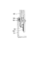
本発明に係わる従来例として、CRTの電気的アース接地構造を図17を参照して説明する。図17は、従来例の画像表示装置の縦断面図であり、一般的なCRTの断面図を示している。 As a conventional example according to the present invention, an electrical grounding structure of a CRT will be described with reference to FIG. FIG. 17 is a longitudinal sectional view of a conventional image display device, and shows a sectional view of a general CRT.
図17において、1700は内部に画像表示のための蛍光体と導電膜を形成したフェースプレート、1701はCRTの真空容器を構成するファンネル、1702は防爆用の金属性テンションバンド、1703はテンションバンド1702の外周に形成された取付け耳部で、この取付け耳部1703を介してCRTはテレビなどの画像表示装置の筐体内に組み込まれる。
In FIG. 17,
1704は前記ファンネルの外壁に形成されたカーボン等を含む低抵抗膜で、後述の高圧印加部1707の周辺を除くファンネル部全周に渡り塗布されている。1705は前記金属性テンションバンド(防爆バンド)1702や低抵抗膜1704を筐体のアースに接地するためのGNDケーブル、1706はアースを表わすが具体的には前記GNDケーブルの端部を筐体内部の電気回路のアース電位パターンに端子で接続している(図示せず)。
1707はフェースプレートの導電膜に高電圧を印加するための高圧印加部で、絶縁性のキャップ内部に電気接続構造を有している。1708は一端を高圧印加部接続し、もう一端を高圧電源(図示せず)に接続した高圧ケーブルである。
1709は映像信号に応じて熱電子を発生し加速させる構造を有する電子銃部である。
以上のように、CRTにおいては電子銃とフェースプレート間のファンネル部分および
フェースプレート周囲のテンションバンドに広い面積のアース電位部を構成し、そのアース電位部をGNDケーブルとして利用して電気回路のアース電位に接続している。
As described above, in the CRT, a wide area ground potential portion is formed in the funnel portion between the electron gun and the face plate and the tension band around the face plate, and the ground potential portion is used as a GND cable to ground the electric circuit. Connected to potential.
また、フェースプレートの画像形成用の導電膜への高圧印加は、先のファンネル部のアース電位部を一部を削除した部分から成されている。 Further, the application of high voltage to the conductive film for image formation on the face plate is made up of a portion where the ground potential portion of the previous funnel portion is partially removed.
このように従来のCRTの電気的アース接地構造においては、高圧印加部を取り巻くファンネル部とフェースプレート周辺部から電気的に確実なGNDケーブルによるアース接地が行われていた。 As described above, in the conventional earth ground structure of the CRT, the earth ground by the electrically reliable GND cable is performed from the funnel part surrounding the high voltage application part and the peripheral part of the face plate.
また他の背景技術として、以下に挙げるものがある。例えば特開平4−163833号公報には、線状熱陰極と、複雑な電極構造を真空パネルに内包した平板型電子線画像表示装置が開示されている。 Other background technologies include the following. For example, JP-A-4-163833 discloses a flat-plate electron beam image display device in which a linear hot cathode and a complicated electrode structure are included in a vacuum panel.
一般的に、このような真空パネルを形成する方法としては、電子放出素子を複数MTX状に配置して形成された電子源と電子源を駆動する駆動配線がMTXに形成されたガラス製のリアプレートと画像形成部材が形成されたガラス製のフェースプレートと両者を枠を介して封着材により気密封着されたものや両者のパネル間隔が狭い場合には、封着材のみで気密封着されたものが知られている。封着材には、低融点ガラス材料が用いられこの材料を軟化させるために400℃程度の高温度まで、昇温させるプロセスを経る。この際、フェース及びリアプレート、及び真空パネルを構成するために必要な大気圧支持スペーサや後述するアノード端子など各種構成部材も同時に高温度下にさらされる。 In general, as a method of forming such a vacuum panel, an electron source formed by arranging a plurality of electron-emitting devices in the form of MTX and a drive wiring for driving the electron source are formed on a glass rear. If the plate and the glass faceplate on which the image forming member is formed and both are hermetically sealed with a sealing material through a frame, or if the panel spacing between the two is narrow, only the sealing material is hermetically sealed. Is known. A low-melting glass material is used as the sealing material, and a process of raising the temperature to a high temperature of about 400 ° C. is performed in order to soften the material. At this time, various components such as an atmospheric pressure support spacer and an anode terminal which will be described later are also exposed to a high temperature at the same time.
これらの工程を経て作製されたパネル内部を真空化プロセスにより、真空処理を行い真空パネルを形成する。そして、外部駆動回路とリアプレート側に形成した取り出し配線とを電気的に接続する工程の後、真空パネルを筐体内部に組み込み画像表示装置として完成させる。 The inside of the panel manufactured through these steps is vacuum-processed by a vacuum process to form a vacuum panel. Then, after the step of electrically connecting the external drive circuit and the extraction wiring formed on the rear plate side, the vacuum panel is incorporated in the housing to complete the image display device.
このようにして形成された電子線を用いた画像表示装置においては、2枚のガラスの間(電子源が形成されたリアプレートと画像形成部材が形成されたフェースプレート)に電子を加速するための数百V〜数十kV程度の電圧を印加している状態で、外部信号処理回路からリアプレートの取り出し配線を通じて画像信号を与えて所望の位置の電子を放出させ、2枚のガラスの間での電位差により電子は加速されフェースプレートの画像形成部材を発光させて、画像として得るものである。上述した電圧は、画像形成部材として通常の蛍光体を用いる場合、好ましい色の発光を得るためには、できるだけ高くすることが好ましく、少なくとも数kV程度であることが望ましい。上述の画像形成部材に数kV程度の電圧を供給するために、放電や高電圧に対して配慮された電圧供給端子の接続構造が求められる。 In an image display device using an electron beam formed in this way, electrons are accelerated between two glasses (a rear plate on which an electron source is formed and a face plate on which an image forming member is formed). In a state where a voltage of about several hundred volts to several tens of kV is applied, an image signal is given from the external signal processing circuit through the rear plate take-out wiring to emit electrons at a desired position, and between the two glasses Electrons are accelerated by the potential difference at, and the image forming member of the face plate emits light to obtain an image. In the case of using a normal phosphor as an image forming member, the above-described voltage is preferably as high as possible, and preferably at least about several kV, in order to obtain light emission with a preferable color. In order to supply a voltage of about several kV to the above-described image forming member, a connection structure of a voltage supply terminal considering electric discharge and high voltage is required.
このような画像表示装置には、画像形成部材に高圧を供給するアノード取り出し部を備える構造を有している。 Such an image display device has a structure including an anode take-out portion that supplies a high pressure to the image forming member.
特許文献1に記載されているアノード端子の構造では、画像表示装置の高圧発生電源より供給される高電圧を高圧ケーブルにて、リアプレート側のアノード取り出し部へ供給し、導入線を通して、フェースプレートに形成された画像形成部材から引き出された配線と接続してフェースプレートの画像形成部材に供給している。
In the structure of the anode terminal described in
また、他の背景技術として、特許文献2がある。ここでは電子放出素子を設けた電子源基板を貫通して高圧を供給する構成が開示される。
Moreover, there exists
また、特許文献3がある。これには液晶パネルのコントロール基板の接地端子をクリップに接触させ、さらにクリップを枠状部材に接触させて接地する構成が開示されている。 Moreover, there exists patent document 3. FIG. This discloses a configuration in which a ground terminal of a control board of a liquid crystal panel is brought into contact with a clip, and further, the clip is brought into contact with a frame member to be grounded.
また、特許文献4にはCRTのアース部材の構造が開示されている。
本願は、電子放出素子及び加速電極を有する電子線装置もしくは画像表示装置の発明であって、異常放電を抑制できる構成を実現することを一つの課題とする発明を含んでいる。また、電子線装置もしくは画像表示装置の発明であって、所定の配線に例えばグランド電位などの所定の電位を簡略及び/または確実に印加できる構成を実現することを一つの課題とする発明を含んでいる。 The present application includes an invention of an electron beam apparatus or an image display apparatus having an electron-emitting device and an acceleration electrode, and an object of the present invention is to realize a configuration capable of suppressing abnormal discharge. In addition, the invention includes an invention of an electron beam apparatus or an image display apparatus, which realizes a configuration capable of simply and / or reliably applying a predetermined potential such as a ground potential to a predetermined wiring. It is out.
本願に係る電子線装置の発明の一つは以下のように構成される。 One of the inventions of the electron beam apparatus according to the present application is configured as follows.
電子線装置であって、
電子放出素子と、
該電子放出素子に接続される駆動配線と、
前記電子放出素子と前記駆動配線が配置される電子源基板と、
前記電子源基板に対向する位置に設けられ、前記電子放出素子が放出する電子を加速する加速電位が与えられる加速電極と、
前記加速電極に前記加速電位を与えるための経路であって、前記電子源基板側の経由部を経由して導出される電位供給経路と、
前記駆動配線とは別に設けられる第1配線であって、前記経由部と前記駆動配線との間の沿面上に設けられる第1配線と、
該第1配線と前記経由部の間の沿面上に設けられる周期的な凹凸構造と、
を有することを特徴とする電子線装置。
An electron beam device,
An electron-emitting device;
Drive wiring connected to the electron-emitting device;
An electron source substrate on which the electron-emitting device and the drive wiring are disposed;
An accelerating electrode provided at a position facing the electron source substrate and applied with an accelerating potential for accelerating electrons emitted from the electron-emitting device;
A path for applying the accelerating potential to the accelerating electrode, and a potential supply path that is derived via a transit part on the electron source substrate side;
A first wiring provided separately from the drive wiring, the first wiring provided on a creeping surface between the transit portion and the drive wiring;
A periodic concavo-convex structure provided on a creeping surface between the first wiring and the transit portion;
An electron beam apparatus comprising:
また本願は電子線装置の発明として以下の構成のものを含んでいる。 The present application also includes the following configuration as an invention of an electron beam apparatus.
電子線装置であって、
電子放出素子と、
該電子放出素子に接続される駆動配線と、
前記電子放出素子と前記駆動配線が配置される電子源基板と、
前記電子源基板に対向する位置に設けられ、前記電子放出素子が放出する電子を加速する加速電位が与えられる加速電極と、
前記加速電極に前記加速電位を与えるための経路であって、前記電子源基板を貫通して導出される電位供給経路と、
前記駆動配線とは別に設けられる第1配線であって、前記経由部と前記駆動配線との間の沿面上に設けられる第1配線と、
前記電位供給経路と一体化されており、前記電子源基板に設けられた孔に気密に装着される封止構造と、
該封止構造と前記第1配線の間の沿面上に設けられる凹凸構造と、
を有することを特徴とする電子線装置。
An electron beam device,
An electron-emitting device;
Drive wiring connected to the electron-emitting device;
An electron source substrate on which the electron-emitting device and the drive wiring are disposed;
An accelerating electrode provided at a position facing the electron source substrate and applied with an accelerating potential for accelerating electrons emitted from the electron-emitting device;
A path for applying the accelerating potential to the accelerating electrode, the potential supplying path being led through the electron source substrate;
A first wiring provided separately from the drive wiring, the first wiring provided on a creeping surface between the transit portion and the drive wiring;
A sealing structure integrated with the potential supply path and hermetically mounted in a hole provided in the electron source substrate;
An uneven structure provided on a creeping surface between the sealing structure and the first wiring;
An electron beam apparatus comprising:
これらの発明においては、凹凸を有することにより効果的に異常放電を抑制することができる。これら凹凸構造を要件とする発明においても、上述もしくは後述の各発明、特には第1配線の構成に関する発明、例えば、第1配線が経由部を隙間無く囲む構成の発明や、第1配線に与える電位に関する各発明や、第1配線の形状に関する各発明や、第1配線をアース接続する発明を組み合わせて用いると好適である。 In these inventions, abnormal discharge can be effectively suppressed by having the irregularities. In the inventions that require these concavo-convex structures as well, the inventions described above or below, in particular, inventions related to the configuration of the first wiring, for example, the invention of the configuration in which the first wiring surrounds the via portion without a gap, or the first wiring It is preferable to use a combination of the inventions related to potential, the inventions related to the shape of the first wiring, and the invention of grounding the first wiring.
また以上の各発明において、前記第1配線は、前記電子放出素子及び前記加速電極及び前記第1配線を内包する真空容器の外部に引き出されており、該引き出し部分に導電性接触部材が接触しており、該導電性接触部材を介して前記第1配線に所定の電位が与えられる構成とすると好適である。 In each of the above inventions, the first wiring is drawn out of a vacuum vessel containing the electron-emitting device, the acceleration electrode, and the first wiring, and a conductive contact member is in contact with the drawn portion. It is preferable that a predetermined potential is applied to the first wiring via the conductive contact member.
特に、前記導電性接触部材が弾性部を有しており、該弾性部の弾性により前記第1配線の引き出し部を押し付けるものであると好適である。接触部材が弾性部を持つ構造とする(例えば弾性を有する金属で接触部材を構成する)ことにより、接触部材が第1配線の引き出し部を弾性により押し付けることができ、確実な接触が実現できる。 In particular, it is preferable that the conductive contact member has an elastic part, and the lead part of the first wiring is pressed by the elasticity of the elastic part. By adopting a structure in which the contact member has an elastic portion (for example, the contact member is made of an elastic metal), the contact member can elastically press the lead portion of the first wiring, and reliable contact can be realized.
また、前記導電性接触部材は、前記電子源基板上の前記第1配線の引き出し部を前記電子源基板とともに挟む構造である構成を好適に採用できる。特に、前記導電性接触部材として、互いに向かい合う対向部を有しており、前記電子源基板を挟み込んでいない状態においては、該対向部の先端間の対向間隔が前記電子源基板の板厚よりも広く、前記第1配線引き出し部と接触する部分の対向間隔が前記電子源基板の板厚よりも狭いものを採用すれば、簡易にかつ確実に接続することができ、所定電位の供給を簡易にかつ確実に行うことができる。 In addition, the conductive contact member can suitably employ a configuration in which the lead portion of the first wiring on the electron source substrate is sandwiched with the electron source substrate. In particular, the conductive contact member has opposing portions facing each other, and when the electron source substrate is not sandwiched, the opposing interval between the tips of the opposing portions is larger than the plate thickness of the electron source substrate. If a wide gap between the portions in contact with the first wiring lead-out portion is smaller than the plate thickness of the electron source substrate, it is possible to easily and surely connect and easily supply a predetermined potential. And it can be done reliably.
また、前記加速電極が設けられる加速電極基板に前記加速電極とは別の第2配線が設けられている構成において、前記導電性接触部材が前記第1配線の引き出し部と前記第2配線の引き出し部の双方に電気的に接続する構成を好適に採用できる。特に、前記導電性接触部材は、前記電子源基板と前記加速電極基板の間に少なくともその一部が挟まれ、前記電子源基板上の前記第1配線の引き出し部と前記加速電極基板上の前記第2配線の引き出し部の双方に接触する構成を好適に採用できる。 Further, in the configuration in which the second wiring different from the acceleration electrode is provided on the acceleration electrode substrate on which the acceleration electrode is provided, the conductive contact member is provided with the lead portion of the first wire and the lead of the second wire. A configuration that is electrically connected to both of the parts can be suitably employed. In particular, the conductive contact member is at least partially sandwiched between the electron source substrate and the acceleration electrode substrate, and the lead-out portion of the first wiring on the electron source substrate and the acceleration electrode substrate A configuration that contacts both of the lead portions of the second wiring can be suitably employed.
弾性により配線引き出し部を押し付ける(もしくは、押し付けかつ挟み込む)構成だけでなく、前記導電性接触部材を導電性及び粘着性を有する部分を有するものとし、該粘着性を有する部分が前記第1配線の引き出し部と接触する構成を好適に採用できる。特に、前記第1配線に所定の電位を印加するための経路となる他の部材と、前記導電性接触部材において粘着性を有する他の部分とが接触している構成を好適に採用できる。粘着性を有する部分を有する導電性接触部材としては金属部材と導電性粘着層を積層した構造を好適に採用できる。このような金属部材としては銅を採用できる。また導電性粘着層としてはカーボンを含有するものが採用できる。 In addition to the configuration in which the wiring lead-out portion is pressed (or pressed and sandwiched) by elasticity, the conductive contact member has a portion having conductivity and adhesion, and the portion having the adhesion is the first wiring. A configuration in contact with the drawer portion can be suitably employed. In particular, it is possible to suitably employ a configuration in which another member serving as a path for applying a predetermined potential to the first wiring is in contact with another portion having adhesiveness in the conductive contact member. As the conductive contact member having an adhesive portion, a structure in which a metal member and a conductive adhesive layer are laminated can be suitably employed. Copper can be used as such a metal member. Moreover, what contains carbon is employable as a conductive adhesive layer.
また、導電性接触部材を配線引き出し部と接触させる上記各発明においては、前記導電性接触部材は、前記第1配線と同一面に引き出された引き出し部と接触するようにすると特に好適である。 In each of the above inventions in which the conductive contact member is in contact with the wiring lead portion, it is particularly preferable that the conductive contact member is in contact with the lead portion drawn out on the same plane as the first wiring.
また、上記第1配線やもしくは第2配線に所定の電位、特にはグランド電位を与える場合、電子線装置のカバーを介して所定電位を与える構成を好適採用できる。カバーを金属により構成したり、カバーを導電性膜で被覆するなどして導電性を有するものとし、導電性接触部材をカバーに固定する(ねじ止めにより固定したり、押し付けることにより固定するなど)などにより電気的に接続して、カバーを介して例えばグランド電位といった所定電位を与える構成を好適に採用できる。カバーの材質としてはアルミニウムやマグネシ
ウムを用いると好適である。また、押し出し加工により成型したものを好適に用いることができる。また樹脂に導電層を設けた導電性カバーを採用することができ、この導電層としては、銅、ニッケル、カーボンの少なくともいずれかを含むものを好適に用いることができる。また、この導電性カバーはこの電子線装置の電源と共通のアース配線に接続する構成を好適に採用できる。
In addition, when a predetermined potential, particularly a ground potential, is applied to the first wiring or the second wiring, a configuration in which the predetermined potential is applied through the cover of the electron beam apparatus can be suitably employed. The cover is made of metal, or the cover is covered with a conductive film to have conductivity, and the conductive contact member is fixed to the cover (fixed by screwing, or fixed by pressing). For example, a configuration in which a predetermined potential such as a ground potential is applied through a cover can be suitably employed. It is preferable to use aluminum or magnesium as the cover material. Moreover, what was shape | molded by the extrusion process can be used suitably. Moreover, the electroconductive cover which provided the electroconductive layer in resin can be employ | adopted, As this electroconductive layer, what contains at least any one of copper, nickel, and carbon can be used suitably. In addition, the conductive cover can be preferably configured to be connected to a ground wire common to the power source of the electron beam apparatus.
また、前記導電性接触部材は、電気ケーブルを接続し、該電気ケーブルを介して前記導電性接触部材に所定電位が与えられるようにしてもよい。導電性接触部材と電気ケーブルの接続は半田付けにより好適に実現できる。また導電性接触部材を介して第1配線をアース接続する場合、導電性接触部材をこの電子線装置の電源のアースに電気的に接続する構成を好適に採用できる。電源のアースをとる構成と第1配線のためのアースをとる構成を共通化できるため、好適である。 The conductive contact member may be connected to an electric cable, and a predetermined potential may be applied to the conductive contact member via the electric cable. The connection between the conductive contact member and the electric cable can be suitably realized by soldering. Further, when the first wiring is connected to the ground via the conductive contact member, a configuration in which the conductive contact member is electrically connected to the ground of the power source of the electron beam apparatus can be suitably employed. Since the configuration for grounding the power supply and the configuration for grounding the first wiring can be made common, it is preferable.
また以上の各発明で、前記第1配線の引き出し部と前記駆動配線の引き出し部とが共通のフレキシブルプリンテッドサーキットに接続されている構成を好適に採用できる。第1配線の引き出し部及び/もしくは駆動配線の引き出し部とフレキシブルプリンテッドサーキットとは導電性接着剤を介して接続されていると好適であり、特には異方性導電テープを用いて配線の引き出し部とフレキシブルプリンテッドサーキットとを接続する構成が好適である。 In each of the above inventions, a configuration in which the lead portion of the first wiring and the lead portion of the drive wiring are connected to a common flexible printed circuit can be suitably employed. The lead-out portion of the first wiring and / or the lead-out portion of the drive wiring and the flexible printed circuit are preferably connected via a conductive adhesive, and in particular the lead-out of the wiring using an anisotropic conductive tape. The structure which connects a part and a flexible printed circuit is suitable.
また以上の各発明において、前記加速電極を設ける加速電極基板が真空容器の一部を構成しており、該加速電極基板の真空容器外面に導電層を有する構成を好適に採用できる。この導電層はフィルム状の物を基板に貼り合わせて形成してもよい。また、画像表示装置として用いる場合で、かつ該導電層の側から画像を見る場合にはこの導電層は透明なものがよい。この導電層としてはITO(Indium Tin Oxide:インジウムティンオキサイド)を用いる構成が好適である。 In each of the above inventions, an acceleration electrode substrate on which the acceleration electrode is provided constitutes a part of a vacuum vessel, and a configuration having a conductive layer on the outer surface of the vacuum vessel of the acceleration electrode substrate can be suitably employed. This conductive layer may be formed by attaching a film-like material to a substrate. Further, when used as an image display device and when an image is viewed from the conductive layer side, the conductive layer is preferably transparent. As this conductive layer, a configuration using ITO (Indium Tin Oxide) is suitable.
また、このように加速電極基板に設けられる導電層を介して前記第1配線に所定の電位が与えられるにする構成を好適に採用できる。なお、第1配線と導電層の接続には前述及び後述の導電性接触部材を用いることができ、特に好適には導電性テープを用いることができ、また、粘着性を有する部分を持つ導電性テープを用いる構成が特に好適である。 In addition, a configuration in which a predetermined potential is applied to the first wiring via the conductive layer provided on the acceleration electrode substrate can be suitably employed. In addition, the conductive contact member mentioned above and below can be used for the connection between the first wiring and the conductive layer, and a conductive tape can be particularly preferably used. A configuration using a tape is particularly suitable.
また加速電極基板に設けられる前記導電層は、前記加速電極基板でその一部が構成される真空容器の少なくとも一部を覆う導電性カバーと電気的に接続されている構成を好適に採用できる。前記導電層と前記導電性カバーの電気的接続は、弾性と導電性とを有する部材により行う構成を好適に採用できる。弾性と導電性とを有する部材としては、導体を弾性体で支持した部材を好適に採用できる。導体としては例えば金属ワイヤを用いることができる。導体を弾性体で支持(特に好適には導体の周囲を弾性体により支持)することにより確実な電気的接続を実現できる。 In addition, the conductive layer provided on the acceleration electrode substrate can be preferably configured to be electrically connected to a conductive cover that covers at least a part of a vacuum vessel part of which is formed by the acceleration electrode substrate. For the electrical connection between the conductive layer and the conductive cover, a configuration in which a member having elasticity and conductivity is used can be suitably employed. As a member having elasticity and conductivity, a member in which a conductor is supported by an elastic body can be suitably employed. For example, a metal wire can be used as the conductor. A reliable electrical connection can be realized by supporting the conductor with an elastic body (particularly preferably, the periphery of the conductor is supported by the elastic body).
また本願は、電子線装置の発明として以下の構成のものを含んでいる。 The present application also includes the following configuration as an invention of the electron beam apparatus.
電子線装置であって、
電子放出素子と、
該電子放出素子に接続される駆動配線と、
前記電子放出素子と前記駆動配線が配置される電子源基板と、
該電子源基板に対向して設けられる加速電極基板と、
該加速電極基板に設けられ、前記電子放出素子が放出する電子を加速する電位が与えられる加速電極と、
該加速電極に前記加速電位を与えるための経路であって、前記電子源基板側の経由部を
経由して導出される電位供給経路と、
前記駆動配線とは別に設けられる第1配線であって、前記経由部と前記駆動配線との間の沿面上に設けられる第1配線と、
加速電極基板上の前記加速電極の周囲に前記加速電極とは別に設けられる第2配線と、を有しており、
前記電子源基板と前記加速電極基板の間でかつ周辺枠部で囲まれる空間は真空雰囲気に維持されており、前記第1配線の引き出し部が前記真空雰囲気外に導出されており、かつ、前記第2配線の引き出し部が前記真空雰囲気外に導出されており、導電性接触部材が前記第1配線の前記引き出し部と前記第2配線の前記引き出し部とに接触していることを特徴とする電子線装置。
An electron beam device,
An electron-emitting device;
Drive wiring connected to the electron-emitting device;
An electron source substrate on which the electron-emitting device and the drive wiring are disposed;
An acceleration electrode substrate provided facing the electron source substrate;
An acceleration electrode provided on the acceleration electrode substrate, to which a potential for accelerating electrons emitted from the electron-emitting device is applied;
A path for applying the accelerating potential to the accelerating electrode, the potential supply path being led out via a transit part on the electron source substrate side;
A first wiring provided separately from the drive wiring, the first wiring provided on a creeping surface between the transit portion and the drive wiring;
A second wiring provided separately from the acceleration electrode around the acceleration electrode on the acceleration electrode substrate;
A space between the electron source substrate and the accelerating electrode substrate and surrounded by a peripheral frame is maintained in a vacuum atmosphere, a lead-out portion of the first wiring is led out of the vacuum atmosphere, and The lead portion of the second wiring is led out of the vacuum atmosphere, and the conductive contact member is in contact with the lead portion of the first wire and the lead portion of the second wire. Electron beam equipment.
なお以上述べた各発明は、加速電位として、駆動配線に電子放出素子を駆動するために与えられる電位のうちの最低電位よりも3kV以上高い電位を与える構成、更には5kV以上高い電圧を印加する構成において特に好適に採用できる。 In each of the inventions described above, a configuration in which a potential higher by 3 kV or more than the lowest potential among the potentials applied to drive the electron-emitting device is applied to the drive wiring as the acceleration potential, and a voltage higher by 5 kV or more is applied. It can employ | adopt especially suitably in a structure.
また本願は、画像表示装置の発明の一つとして上述の電子線装置と、該電子線装置が有する電子放出素子が放出する電子が照射されることにより発光する蛍光体とを有する画像表示装置の発明を含んでいる。 The present application also relates to an image display apparatus comprising the above-described electron beam apparatus as one of the inventions of the image display apparatus, and a phosphor that emits light when irradiated with electrons emitted from the electron-emitting devices of the electron beam apparatus. Includes invention.
本願にかかわる発明によると、異常放電を抑制できる。また、本願に係る発明の一つによると異常放電を抑制する構造への所定電位、特にはアース電位の供給を確実に及びまたは容易及びまたは生産性良く行うことが出来る。 According to the invention of the present application, abnormal discharge can be suppressed. Further, according to one of the inventions according to the present application, it is possible to reliably and / or easily and / or improve the supply of a predetermined potential, particularly a ground potential, to the structure for suppressing abnormal discharge.
以下では本願発明の実施の形態を詳細に説明する。なお以下の実施の形態において特に考慮した点は以下のとおりである。 Hereinafter, embodiments of the present invention will be described in detail. The following points are particularly considered in the following embodiments.
平板型の薄型画像表示装置の場合、放電の発生する危険が大きくなる。放電が発生した場合には、瞬間的に極めて大きな電流が流れるが、この一部分が電子源の駆動配線に流れ込むと、電子源の電子放出素子に大きな電圧がかかる。この電圧が通常の動作において印加される電圧を越えると、電子放出特性が劣化してしまう場合があり、さらには素子が破壊される場合もある。このようになると、画像の一部が表示されなくなり、画像の品位が低下し、画像表示装置として使用することができなくなる。 In the case of a flat-type thin image display device, the risk of discharge is increased. When a discharge occurs, an extremely large current flows instantaneously. However, when a part of the current flows into the drive wiring of the electron source, a large voltage is applied to the electron-emitting device of the electron source. If this voltage exceeds the voltage applied in normal operation, the electron emission characteristics may be deteriorated, and the device may be destroyed. In this case, a part of the image is not displayed, the quality of the image is deteriorated, and the image display device cannot be used.
一方、平面型の画像表示装置は、壁掛けが可能なことから軽量化が求められている。狭額縁(額縁=画像領域より外側の領域)化は、視聴者に対する商品価値のみでなく、軽量化に対して大きく寄与するものである。しかしながら、高電圧を印加する平面型画像表示装置では、放電に危険があるため、従来は沿面距離を確保する上で極端に狭くできなかった。 On the other hand, the flat type image display device is required to be lightweight because it can be wall-mounted. The narrow frame (frame = area outside the image area) greatly contributes not only to product value for the viewer but also to weight reduction. However, in a flat-type image display device to which a high voltage is applied, since there is a risk of discharge, conventionally, it has not been possible to make it extremely narrow in order to secure a creepage distance.
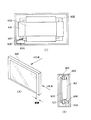
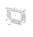
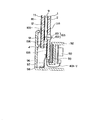
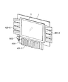
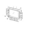
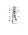
以下にこの実施形態の詳細を述べる。図1は、本発明の画像表示装置の構成の一例を模式的に示す分解斜め模式図である。図2は図1のA矢視方向からみたアノード端子部の断面を示した部分断面図であり、図3A〜Eは、リアプレート基板の作製工程を説明する図で電子源領域の一部分を用いた。図4はリアプレートのアノード端子部周辺部を示した平面図である。 Details of this embodiment will be described below. FIG. 1 is an exploded oblique schematic view schematically showing an example of the configuration of the image display apparatus of the present invention. FIG. 2 is a partial cross-sectional view showing a cross section of the anode terminal portion viewed from the direction of arrow A in FIG. 1, and FIGS. 3A to 3E are diagrams for explaining a manufacturing process of the rear plate substrate and use a part of the electron source region. It was. FIG. 4 is a plan view showing the periphery of the anode terminal portion of the rear plate.
1は電子源を形成するための電子源基板と真空容器の一部とを兼ねるリアプレート、2は電子源領域で、電界放出素子、表面伝導型電子放出素子などの電子放出素子を複数配置し、目的に応じて駆動できるように素子に接続された駆動配線を形成したものである。
駆動配線は電子源領域内に位置する部分と引き出し部3−1,3−2を有しており、駆動配線引き出し部3−1,3−2により画像表示装置の外部に取り出され、電子源の駆動回路に接続される。11は画像形成部材が形成されたフェースプレート、12は電子源領域2より放出された電子により発光する蛍光体及び加速電極であるメタルバックを含む画像形成部材、100は画像形成部材12のメタルバックに加速電位を供給するために引き出されたAg(銀)ペースト等を焼成して形成した引き出し配線、4はリアプレート1とフェースプレート11に挟持される外枠であり、電子源駆動配線引き出し部3は外枠4とリアプレート1の接合部で、例えば低融点ガラス(フリットガラス201)に埋設されて外部に引き出される。リアプレート1及びフェースプレート11及び外枠4の材料として、青板ガラス、表面にSiO2被膜を形成した青板ガラス、Naの含有量を少な
くしたガラス、石英ガラスなど、条件に応じて各種材料を用いる。
The drive wiring has a portion located in the electron source region and lead-out portions 3-1, 3-2, and is taken out of the image display device by the drive wiring lead-out portions 3-1, 3-2, and the electron source Connected to the driving circuit. 11 is a face plate on which an image forming member is formed, 12 is an image forming member including a phosphor that emits light by electrons emitted from the
101は外部の高圧電源より供給された電位を導入するための電位供給経路である導入線、102は導入線101をあらかじめAg−Cu、Au−Niなどのろう材料を使用し気密シール処理を施して柱状形状の中心に一体形成する絶縁部材である。
絶縁部材102の材料として、アルミナ等のセラミック、Na含有量の少ないガラスなど、リアプレート1材料の熱膨張係数に近い材料でかつ、高電圧に耐える絶縁性を有する材料で、かつ高温度になった場合の熱膨張差による絶縁部材102とリアプレート1との接合部での割れを防止できる材料を選択するとよい。
The material of the insulating
なお、このような構成をもつ高圧端子以外の構成でもよく、この構成に限定されるものではない。また、導入線101と引き出し配線100との接続を確実にするために、導入線101と引き出し配線100との間にAgペーストや機械的なばね構成などの接続部材を配置構成してもよい。
A configuration other than the high voltage terminal having such a configuration may be used, and the configuration is not limited to this configuration. In order to ensure the connection between the lead-in
導入線101と絶縁部材102とで一体化構造である気密導入端子103を構成する。
The lead-in
104はリアプレート1に形成された孔であり、気密導入端子103を貫入する孔である。気密導入端子103とリアプレート1に形成した貫通孔104との間は、フリットガラス201などの気密化が可能な接着部材にて固定する。
A
なお、貫通孔104の形成場所として、リアプレートの駆動用配線引き出し部3−1,3−2の形成されていない4隅でかつ、外枠4の内側に配置構成される。
The through
さらに、数kVの高電圧が導入線101を通して印加された時の放電抑制構造として、第1配線である独立配線105を駆動配線引き出し部3−1,3−2が設けられていない位置に導入線101が絶縁部材102を貫通する位置(経由部)を同心円状に取り囲むようにリング状に形成する。
Furthermore, as a discharge suppression structure when a high voltage of several kV is applied through the lead-in
リング状に形成することで、リング周辺部に電極エッジなどが形成されていても、異常放電を生じにくい構成とすることができる。なお、取り囲む形状については、多角形形状が考えられるが電界集中の観点からリング状が好ましい。また完全に取り囲むのが望ましいが、一部すきまが空いていてもよい。また独立配線105は囲む形状にしなくてもよく、経由部と駆動配線の間で、それらの間隔が最も短い部分に少なくとも設けられているとよい。
By forming in a ring shape, even if an electrode edge or the like is formed in the periphery of the ring, a configuration in which abnormal discharge hardly occurs can be obtained. In addition, although the polygonal shape can be considered about the surrounding shape, a ring shape is preferable from a viewpoint of electric field concentration. Moreover, it is desirable to completely surround, but a part of the clearance may be vacant. Further, the
ただし、狭額縁になると、外枠4の加工のばりやフリット封着材料のはみ出し形状、駆動配線の形状などの影響を考慮することが望ましく取り囲む構成、特には完全に取り囲む
構成が望ましい。次に、独立配線105と気密導入端子103の導入線101との間を高抵抗膜(=耐圧構造106)で電気的に導通させてつなげた電位規定構造を配置する。
However, in the case of a narrow frame, it is desirable to take into account the influence of the processing burr of the
その他の耐圧構造として、凹凸構造の形成による沿面距離の増大などの形態をとれる。 As another pressure-resistant structure, it is possible to take a form such as an increase in creepage distance due to formation of an uneven structure.
この耐圧構造106により所望の高電圧に対して十分な耐圧を確保できるため放電によって電子源領域へ放電電流が流れ、素子が劣化するなどのダメージが起こらない構成とすることができる。同時に、高圧導入部形成領域を最小限に小さくしても放電を抑制できることから、真空内部の画像形成部材12から外枠4より内側までの距離を小さくすることが可能となる。高抵抗膜の材料としては、窒化物、酸化物、炭化物などの膜材料があげられる。
Since the withstand
つづいて、5は真空化するための排気孔、6は排気孔5に対応する位置に配置するガラス管で、不図示の外部真空形成装置に接続され、電子放出素子を形成する真空処理が終了後封止するためのものである。なお、この他真空装置内で画像表示装置を組立てる方法をとれば、上述のガラス管6並びに、排気孔5は不要となる。 Next, 5 is an exhaust hole for evacuation, and 6 is a glass tube disposed at a position corresponding to the exhaust hole 5, which is connected to an external vacuum forming apparatus (not shown) and completes the vacuum processing for forming the electron-emitting device. It is for post-sealing. In addition, if the method of assembling an image display apparatus in a vacuum apparatus is taken, the above-mentioned glass tube 6 and the exhaust hole 5 will become unnecessary.
また、本発明に用いる電子源を構成する電子放出素子の種類は、電子放出特性や素子のサイズ等の性質が目的とする画像表示装置に適したものであれば、特に限定されるものではない。熱電子放出素子、あるいは電界放出素子、半導体電子放出素子、MIM型電子放出素子、表面伝導型電子放出素子などの冷陰極素子等が使用できる。 In addition, the type of the electron-emitting device constituting the electron source used in the present invention is not particularly limited as long as properties such as electron emission characteristics and device size are suitable for the intended image display apparatus. . Thermionic emission devices, or cold cathode devices such as field emission devices, semiconductor electron emission devices, MIM type electron emission devices, and surface conduction type electron emission devices can be used.
後述する実施例において示される表面伝導型電子放出素子は本発明に好ましく用いられるものであるが、上述の本出願人による出願、特開平7−235255号公報に記載されたものと同様のものである。 The surface conduction electron-emitting devices shown in the examples described later are preferably used in the present invention, but are the same as those described in the above-mentioned application by the present applicant, Japanese Patent Application Laid-Open No. 7-235255. is there.
以下、実施例に基づき、本発明の特徴をさらに詳細に説明する。 Hereinafter, based on an Example, the characteristic of this invention is demonstrated in detail.
(第1の参考例)
図面により具体的に説明する。図1は、本発明の画像表示装置の構成の一例を模式的に示す分解斜め模式図である。
(First reference example)
This will be specifically described with reference to the drawings. FIG. 1 is an exploded oblique schematic view schematically showing an example of the configuration of the image display apparatus of the present invention.
図2は図1のA矢視方向からみた図であり、特にアノード端子部の断面を示した断面図であり、図3A〜Eは、リアプレート基板の作成工程を説明する図で電子源領域の一部分を用いた。図4はリアプレートのアノード端子部周辺部を示した平面図である。 2 is a view as seen from the direction of arrow A in FIG. 1, and particularly is a cross-sectional view showing a cross-section of the anode terminal portion. FIGS. A part of was used. FIG. 4 is a plan view showing the periphery of the anode terminal portion of the rear plate.
図5は、真空パネルのフェースプレートを取り除いた状態でのアノード端子部周辺部を示した平面図である。図6は、平面型画像表示装置の略内部構造を示す図である。 FIG. 5 is a plan view showing the periphery of the anode terminal portion with the face plate of the vacuum panel removed. FIG. 6 is a diagram showing a substantially internal structure of the flat image display device.
図1において、1は電子源を搭載した青板ガラス材料で形成したリアプレート、2は電子源領域で、特開平7−235255号公報に記載される表面伝導型電子放出素子をマトリクス状に配列している。電子源領域では駆動配線である走査配線と変調配線により電子放出素子がマトリクス接線されている。電子源領域の駆動配線は印刷により形成した駆動配線引き出し部によりX,Yの4方向に真空容器の外部に引き出される。フレキシブル配線により駆動配線引き出し部3と電子源の駆動回路が接続される。
In FIG. 1,
11は画像形成部材12を搭載した加速電極基板であり、フェースプレートとして真空容器の一部を構成する。
青板ガラス材料で形成されている。100は画像形成部材12の1隅から引き出したA
g材料からなる印刷により形成した引き出し配線で、その形成場所は、リアプレート1に形成した貫通孔より導入される高圧端子の導入線と当接可能な位置に形成した。
It is made of blue plate glass material. 100 denotes A drawn from one corner of the
The lead-out wiring formed by printing made of the g material was formed at a position where it could come into contact with the introduction line of the high-voltage terminal introduced from the through hole formed in the
引き出し配線100は画像形成部材12のメタルバックに重なるように印刷形成することで、電気的導通を確保した。また、画像形成部材12はストライプ状の蛍光体、ブラックストライプ、加速電極であるメタルバックから構成される。蛍光体、ブラックストライプは、印刷により形成し、その後これらの上にメタルバックとしてAl膜を真空蒸着法により形成した。4はリアプレート1とフェースプレート11に挟持される青板ガラス材料よりなる外枠であり、駆動配線引き出し部3−1,3−2は外枠4とリアプレート1の接合部で接合材(日本電気硝子製のLS3081のフリットガラス)201に埋設して外部に引き出した。101は426合金材料よりなる導入線、102は導入線101をあらかじめAg−Cuにてろう付けし、真空気密シール処理を施して柱状形状の中心に一体形成したアルミナセラミック製の絶縁部材、104は導入線101を気密に一体化する絶縁部材102を導入する貫通孔である。貫通孔104の配置場所については、後述する。
The lead-out
つづいて、図1、図3A−E、図4を参照して、リアプレート1の作成手順をさらに詳細に説明する。
Next, the procedure for creating the
(工程−a)
洗浄した青板ガラスの表面に、0.5μmのSiO2層をスパッタリングにより形成し
、リアプレート1とした。つづいて超音波加工機により図1、図4に示す、高圧導入端子の導入のための直径2mmの円形の貫通孔104を形成した。
(Process-a)
A 0.5 μm SiO 2 layer was formed by sputtering on the surface of the washed soda-lime glass, and the
形成場所は、図1,4のように電子源領域2及び駆動配線引き出し部3−1,3−2が形成されていない隅でかつ、後述の独立配線から、6mm離した位置を孔の中心とし配置した。
The formation location is a corner where the
該リアプレート上にスパッタ成膜法とフォトリソグラフィー法を用いて表面伝導型電子放出素子の素子電極21と22を形成する。材質は5nmのTi、100nmのNiを積層したものである。素子電極間隔は2μmとした。(図3A)
(工程−b)
つづいて、Agペーストを所定の形状に印刷し、焼成することにより変調配線であるY方向配線23を形成した。該配線は電子源形成領域の外部まで延長され、該延長部が図1における電子源駆動配線引き出し部3−2となる。
(Process-b)
Subsequently, an Ag paste was printed in a predetermined shape and baked to form a Y-
該配線の幅は100μm、厚さは約10μmである。(図3B)また、Y方向配線形成時に、図4のように独立配線105、独立配線引き出し部A107、独立配線引き出し部B108も同時に形成した。該独立配線105の幅は、0.6mm、厚さは10μmである。独立配線105の直径をφ6.3mm(配線の中央)とした。
The wiring has a width of 100 μm and a thickness of about 10 μm. (FIG. 3B) When forming the Y-direction wiring, the
独立配線引き出し部A107は、電子源駆動用配線3−1,3−2の一番外側に配置し、後述のフレキシブル配線で外部へ取り出すため、駆動用配線と同ピッチの位置に図4,5に示すように外枠4から外側(大気側)で取り出すことができるように配置し、独立配線引き出し部B108は、図5に示すように外枠4の外側(大気側)に位置するように配置構成した。上記駆動配線、独立配線引き出し部は後述の封着工程にて外枠を形成する際に使用するフリットにて埋設され真空気密を維持できる構造となる。
The independent wiring lead-out portion A107 is arranged on the outermost side of the electron source driving wirings 3-1 and 3-2 and is taken out to the outside by a flexible wiring described later. As shown in FIG. 5, it is arranged so that it can be taken out from the
(工程−c)
次に、PbOを主成分とし、ガラスバインダーを混合したペーストを用い、同じく印刷
法により絶縁層24を形成する。これは上記Y方向配線23と後述のX方向配線を絶縁するもので、厚さ約20μmとなるように形成した。なお、素子電極22の部分には切り欠き24Cを設けて、X方向配線と素子電極の接続をとるようにしてある。(図3C)
(Process-c)
Next, the insulating
(工程−d)
つづいて走査配線であるX方向配線25を上記絶縁層24上に形成する(図3D)。方法はY方向配線の場合と同じで、配線の幅は300μm、厚さは約10μmである。該配線は電子源形成領域の外部まで延長され、該延長部が図1における電子源駆動配線引き出し部3−1となる。
(Process-d)
Subsequently, an
つづいて、有機Pd溶液を塗布して、大気中300℃、12分間の焼成を行って、PdOの微粒子膜26を形成する。(図3E)
Subsequently, an organic Pd solution is applied and baked at 300 ° C. for 12 minutes in the atmosphere to form a PdO
以上の工程にて作成されたリアプレート1は、図1及び4のように4隅に配線が形成されない領域を有する。その1隅の駆動配線引き出し部3−1,3−2及び外枠で囲まれる領域に気密導入端子103の導入線101を同心円状に取り囲むように独立配線105を印刷プロセスにてAgペースト材料を焼成して形成配置する。
The
気密導入端子103の導入線101と独立配線105の間に高抵抗膜(WとGeの合金窒化膜)を真空蒸着法にて独立配線105と気密導入端子103の導入線105との間が高抵抗膜を介して電気的につながるように形成する。なお貫通孔104と対向する位置にフェースプレート11の引き出し配線100が位置するように構成している。
A high resistance film (alloy nitride film of W and Ge) is placed between the lead-in
上述のWとGe合金窒化膜はスパッタリング装置を用いてアルゴンと窒素混合雰囲気中でWとGeのターゲットを同時スパッタする事により成膜した。図4の独立配線105の位置に成膜するため、独立配線105の形状にエッチング加工にて作製したメタルマスクを使用し、所望位置に成膜した。それぞれのターゲットにかける電力を変化することにより組成の調節を行い、最適の抵抗値を得た。
The above W and Ge alloy nitride films were formed by simultaneously sputtering a W and Ge target in a mixed atmosphere of argon and nitrogen using a sputtering apparatus. In order to form a film at the position of the
詳述すると、スパッタチャンバの背圧は、2×10のマイナス5乗Paで、スパッタ時には、窒素分圧が30%になるように、アルゴンと窒素の混合ガスを流した。 More specifically, the back pressure of the sputtering chamber was 2 × 10 −5 Pa, and a mixed gas of argon and nitrogen was flowed so that the nitrogen partial pressure was 30% during sputtering.
スパッタガス全圧は0.45Paであった。Wターゲットに15W、Geターゲットに150Wの高周波電力を投入し、スパッタ時間を調整することにより、WとGeの合金窒化膜を作製した。作製したWとGeの合金窒化膜は(膜厚が43nm、比抵抗が250Ωcm、シート抵抗が5.8×10⁹Ω/□)(膜厚が200nm、比抵抗が2.4×105Ωcm、シート抵抗が1.2×1012Ω/□)(膜厚80nmで比抵抗4.5×108Ω
cm、シート抵抗が5.6×10¹⁵Ω/□)の3種である。なお、本参考例では導入線101と独立配線115の間にのみ成膜したが独立配線105の外側周辺部にも成膜してかまわない。
The total sputtering gas pressure was 0.45 Pa. By applying high frequency power of 15 W to the W target and 150 W to the Ge target and adjusting the sputtering time, an alloy nitride film of W and Ge was produced. The produced alloy nitride film of W and Ge (film thickness is 43 nm, specific resistance is 250 Ωcm, sheet resistance is 5.8 × 10 9 Ω / □) (film thickness is 200 nm, specific resistance is 2.4 × 10 5 Ωcm) Sheet resistance is 1.2 × 10 12 Ω / □) (specific resistance 4.5 × 10 8 Ω at a film thickness of 80 nm)
cm and sheet resistance of 5.6 × 10 15 Ω / □). In this reference example, the film is formed only between the lead-in
次に、上記リアプレート1、フェースプレート11、外枠4部材などを用いてパネル化すなわち真空容器形成を行う。組立てに際しては、フェースプレート11の画像形成部材12の蛍光体とリアプレート1の電子放出素子とが相互に対応するように注意深く位置合わせする。
Next, using the
また、気密導入端子103及び、ガラス管6を設置し、かつ上述の位置合わせがなされた状態で、加熱炉へ投入し420度の温度を付与し、フェースプレート11とリアプレート1と外枠4の当接位置に配置したフリットガラス201を溶解させる。
In addition, in the state where the
その後、冷却させて組立てが終了する。この状態で、フェースプレート11、リアプレート1、外枠4、ガラス管6、気密導入端子103を有する気密維持可能なパネルとして形成できた。この後、ガラス管6を介して真空排気装置に接続し、パネル内を排気し、フォーミング処理、活性化処理を各微粒子膜26に対して行う。
Thereafter, the assembly is completed after cooling. In this state, it was possible to form an airtight and maintainable panel having the
つづいて、パネル内の排気継続し、ベーキング処理を行い、真空パネル内に残留した有機物質分子を除去する。最後に、ガラス管6を加熱溶着して封止する。以上の工程にて、真空パネルは完成する。 Subsequently, the exhaust in the panel is continued and baking is performed to remove organic molecules remaining in the vacuum panel. Finally, the glass tube 6 is heat-welded and sealed. The vacuum panel is completed through the above steps.
次に、駆動配線引き出し部3−1,3−2を駆動回路基板と又、独立配線105から引き出した独立配線引き出し部A107を外部のグランド端子とそれぞれ接続するために、FPC(フレキシブルプリンティッドサーキットの略)401を図5の位置に電気的に接続し、かつ固定を行う。この時、FPC実装装置を用いる。
Next, in order to connect the driving wiring lead portions 3-1 and 3-2 to the driving circuit board and the independent wiring leading portion A107 drawn from the
より安定な外部グランド端子との接続を行うために独立配線引き出し部B108においてもグランド端子と接続されたクリップをリアプレート102に挟み込む。
In order to connect to a more stable external ground terminal, the clip connected to the ground terminal is also sandwiched between the
この後、真空パネルの筐体への組み込みと電気ボードとFPCとの接続作業などを行い、平面型画像表示装置が完成する。 Thereafter, the flat panel image display device is completed by incorporating the vacuum panel into the casing and connecting the electric board and the FPC.
図6Aは筐体に真空容器を組み込んだ平面型画像表示装置の構成を示す図である。 FIG. 6A is a diagram illustrating a configuration of a flat-type image display device in which a vacuum container is incorporated in a housing.
図6Bは図6Aを矢印A方向から見た側断面図を示す。図6Cは図6Aを矢印B方向から見た縦断面図を示す。 FIG. 6B shows a side sectional view of FIG. 6A viewed from the direction of arrow A. FIG. 6C shows a longitudinal sectional view of FIG.
601は筐体を構成するカバーである。602が真空容器であり、603は駆動回路を有する駆動回路基板である。フレキシブルプリンテッドサーキット401により駆動配線引き出し部と駆動回路とが接続される。605は導入線101に接続される高圧導入経路である。600は加速電位を発生する高圧電源である。
本参考例において、外部映像を入力し、電子放出素子を駆動して画像表示を行ったところ、異常放電は生じず、安定に画像表示を行うことができた。 In this reference example, when an external image was input and image display was performed by driving the electron-emitting device, abnormal discharge did not occur and image display could be performed stably.
狭額縁の電子線装置及び画像表示装置を実現でき、また、軽量な電子線装置及び画像表示装置を実現できた。 A narrow frame electron beam device and an image display device can be realized, and a lightweight electron beam device and an image display device can be realized.
(第1の実施形態)
図7を用いて、第1の実施形態を説明する。図7は、図1のA矢視方向からみた図であり、特にアノード端子部の断面を示した断面図である。
(First embodiment)
The first embodiment will be described with reference to FIG. FIG. 7 is a view as seen from the direction of arrow A in FIG. 1, and in particular, a cross-sectional view showing a cross section of the anode terminal portion.
第1の実施形態では、独立配線105と気密導入端子103との間の耐圧構造の別の実施形態を説明する。なお、前述した各実施形態と同様な各部には同一符号を付して、その説明とそれらの構成、製造方法などを省略する。
In the first embodiment, another embodiment of the withstand voltage structure between the
気密導入端子103の導入線101と、それを取り囲むように同心円状に形成した独立配線105との間のリアプレート1のガラス面を機械加工し耐圧構造701を加工形成する。
The glass surface of the
構造は、気密導入端子103の中心に対して同心に2重の掘り込み加工を行う。
The structure performs a double digging process concentrically with respect to the center of the
深さは、ガラス厚み2.8mmに対して0.5mm加工し、加工の曲率半径を0.5mmRとした。ピッチは、1.5mmピッチとした。本構成では、実質的に沿面距離を増大させることが可能となった。耐圧構造701を有する真空パネルを図6のように、平面型画像表示装置として組み込み駆動表示を行ったところ、放電の発生もなく安定に駆動できた。
The depth was 0.5 mm with respect to the glass thickness of 2.8 mm, and the curvature radius of the processing was 0.5 mmR. The pitch was 1.5 mm. With this configuration, the creepage distance can be substantially increased. When the vacuum panel having the pressure-
以上説明したように、この構成によれば、リアプレート1側にあらかじめ耐圧構造を形成することで、真空パネル形成プロセスを最小限に抑えることができる長所と、合わせて軽量化平面型画像表示装置として提供することができる。
As described above, according to this configuration, the pressure-resistant structure is formed on the
(第2の参考例)
本参考例で用いる電子線装置の真空容器は、リアプレートとフェースプレートとの距離がわずか数[mm]の真空容器であるため、フェースプレートの画像形成用の加速電極へ加速電位を供給するための構造を設けるスペースを十分に取るのが困難である。該スペースを狭くすると異常放電の可能性が高くなってしまう。
(Second reference example)
Since the vacuum container of the electron beam apparatus used in this reference example is a vacuum container in which the distance between the rear plate and the face plate is only a few [mm], the acceleration potential is supplied to the acceleration electrode for image formation on the face plate. It is difficult to take a sufficient space for providing the structure. Narrowing the space increases the possibility of abnormal discharge.
このような問題は、上述の参考形態や以下の参考例及び実施形態でも示すように、加速電位供給経路における異常放電を抑制できる構成、具体的には、電子源基板における加速電位供給経路の経由部の周りを所定電位を与えた第1配線で囲むこと、更には前記経由部と第1配線の間に双方と電気的に接続する抵抗膜を設けることで抑制できる。 Such a problem is caused by the configuration that can suppress abnormal discharge in the acceleration potential supply path, specifically, the acceleration potential supply path in the electron source substrate, as shown in the above reference form and the following reference examples and embodiments. This can be suppressed by surrounding the portion with a first wiring to which a predetermined potential is applied, and further by providing a resistance film electrically connected to both between the transit portion and the first wiring.
ただし、電子線装置もしくは画像表示装置として用いる場合には、第1配線などに所定の電位、特にはグランド電位を与えるための構成を十分に検討することが望ましい。 However, when used as an electron beam device or an image display device, it is desirable to fully study a configuration for applying a predetermined potential, particularly a ground potential, to the first wiring or the like.
以下の参考例では、特にグランド電位を供給する構造を説明する。この参考例では、薄型平面型の画像表示パネルに電子放出素子を用いたディスプレイを採用し、高圧電源から真空容器内部のフェースプレートの加速電極までの加速電位を印加する経路において、真空容器を構成するリアプレートに加速電位を印加する気密導入端子を設け、該導入線の周囲に高抵抗膜による耐圧構造と、その周囲にリング状の独立配線を構成した。 In the following reference example, a structure for supplying a ground potential will be described. In this reference example, a display using an electron-emitting device is adopted for a thin flat type image display panel, and a vacuum container is configured in a path for applying an acceleration potential from a high voltage power source to an acceleration electrode of a face plate inside the vacuum container. An airtight introduction terminal for applying an accelerating potential is provided on the rear plate, and a withstand voltage structure using a high resistance film is formed around the introduction line, and a ring-shaped independent wiring is formed around the structure.
そして、前記独立配線のアース電位を確実にするため、ドライバー回路のアース電位に接地するFPC(Flexible Printed Circuitフレキシブルプリンテッドサーキット)のアース配線と独立配線の一部を接続し、更に電源部のアースに接地した前フレームと独立配線引き出し部とを導電性接触部材である接触子を介して接触させた。 In order to ensure the ground potential of the independent wiring, a part of the independent wiring and the ground wiring of an FPC (Flexible Printed Circuit Flexible Printed Circuit) grounded to the ground potential of the driver circuit are connected, and further the ground of the power supply unit The front frame that was grounded and the independent wiring lead portion were brought into contact with each other through a contact that was a conductive contact member.
すなわち真空容器の構成要素の少なくとも一部を覆うカバーを兼ねるフレームを介して第1配線を接地する構造としている。前記接触子はばね性を有し前フレームに例えばねじ固定され、独立配線引き出し部を常に押し付ける。更に真空容器は、前フレームと中フレームとで弾性体を介して挟み支持して位置を固定し、前記接触子と独立配線引き出し部との接触位置を合わせた。 That is, the first wiring is grounded via a frame that also serves as a cover that covers at least a part of the components of the vacuum vessel. The contact has springiness and is fixed to the front frame by screws, for example, and always presses the independent wiring lead portion. Further, the vacuum container was sandwiched and supported by the front frame and the middle frame via an elastic body to fix the position, and the contact position between the contact and the independent wiring lead-out portion was adjusted.
なお本参考例で用いる電子源基板、電子放出素子、加速電極基板、加速電極、駆動配線、加速電位供給経路など、真空容器及び電子放出にかかわる構造は第1の参考例、第1の実施形態と同様である。 The structure related to the vacuum vessel and the electron emission, such as the electron source substrate, the electron emission element, the acceleration electrode substrate, the acceleration electrode, the drive wiring, and the acceleration potential supply path used in this reference example, is the first reference example and the first embodiment. It is the same.
その動作原理も第1の参考例、第1の実施形態と同様で、真空空隙を形成した対向する基板間において、背面側のリアプレート(RP)上に各画素位置に電子放出素子を設けている。 The operating principle is the same as in the first reference example and the first embodiment, and an electron-emitting device is provided at each pixel position on the rear plate (RP) on the back side between opposing substrates in which a vacuum gap is formed. Yes.
電子放出素子は、表面伝導型放出素子を用いている。ここでの表面伝導型放出素子は、電子放出のための一対の素子電極(高電位側電極と低電位側電極)を数十[μm]の間隔で対向する形に形成し、導電性膜を対向電極のそれぞれにつながるように配置し、該導電性膜に電子放出部を形成したものである。 A surface conduction electron-emitting device is used as the electron-emitting device. The surface conduction electron-emitting device here is formed by forming a pair of device electrodes for electron emission (a high-potential side electrode and a low-potential side electrode) facing each other at intervals of several tens [μm], and forming a conductive film It is arranged so as to be connected to each of the counter electrodes, and an electron emission portion is formed in the conductive film.
一方対向するフェースプレート(FP)の真空空隙側にはコントラストを向上するためのブラックストライプ膜、三原色RGB各色相の蛍光体膜、更にその上に加速電極となる導電性のメタルバック膜が形成されている。 On the other hand, a black stripe film for improving contrast, a phosphor film for each of the three primary colors RGB, and a conductive metal back film serving as an acceleration electrode are formed on the opposite side of the face plate (FP) on the vacuum gap side. ing.
この電子放出素子の動作は、電気実装回路(駆動回路)で選択したX方向配線とY方向配線間に十数[V]の電圧を掛けて電子放出素子から電子を放出させ、フェースプレートの真空空隙側のメタルバック膜に外部電圧電源から供給された十数[kV]の+電位(加速電位)により前記放出電子が加速されて蛍光体膜に衝突して発光を起す。 The operation of this electron-emitting device is such that electrons are emitted from the electron-emitting device by applying a voltage of more than a dozen [V] between the X-direction wiring and Y-direction wiring selected by the electric mounting circuit (drive circuit), and the face plate vacuum The emitted electrons are accelerated by a plus potential (acceleration potential) of tens [kV] supplied from an external voltage power source to the metal back film on the air gap side and collide with the phosphor film to emit light.
リアプレートと電気実装回路とを接続しているフレキシブルケーブルは、電気実装回路側はコネクターで電気的機械的に接続され、一方のリアプレート側は、異方性導電膜によりこのリアプレート上に印刷されたX方向配線とY方向配線の電極部(配線引き出し部の端部)に電気的機械的に接続されている。 The flexible cable that connects the rear plate and the electrical mounting circuit is electrically and mechanically connected on the electrical mounting circuit side with a connector, and one rear plate side is printed on this rear plate with an anisotropic conductive film. It is electrically and mechanically connected to the electrode portions of the X direction wiring and Y direction wiring (end portions of the wiring lead portions).
フェースプレートのメタルバック膜と高圧電源回路とを接続する高圧ケーブルは、高圧電源回路側は高圧用のコネクターで電気的機械的に接続し、一方のフェースプレート側は、リアプレートに設けた貫通穴に配置した導電線と絶縁体を一体化した気密導入端子を介してメタルバックに電気的機械的に接続している。 The high voltage cable connecting the metal back membrane of the face plate and the high voltage power circuit is electrically and mechanically connected on the high voltage power circuit side with a high voltage connector, and one face plate side is a through hole provided in the rear plate. Are electrically and mechanically connected to the metal back via an airtight introduction terminal in which the conductive wire and the insulator are integrated.
以下に図面を参照して、この参考例を詳しく説明する。ただし、この形態に記載されている構成部品の寸法、材質、形状、その相対配置などは、特に特定的な記載がない限りは、この発明の範囲をそれらのみに限定する趣旨のものではない。 Hereinafter, this reference example will be described in detail with reference to the drawings. However, the dimensions, materials, shapes, relative arrangements, and the like of the component parts described in this embodiment are not intended to limit the scope of the present invention only to those unless otherwise specified.
また、以下の図面において、既述の図面に記載された部材と同様の部材には同じ番号を付す。 Moreover, in the following drawings, the same number is attached | subjected to the member similar to the member described in above-mentioned drawing.
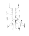
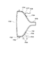
以下に、本発明に係る画像表示装置の第2の参考例について、図5及び図8から図10を参照して説明する。図8は、本発明に係る画像表示装置の第2の参考例を表わす画像表示部の外観図、図9は、図8に示される画像表示装置の画像表示部の要部縦断面図、図10は、図8に示される画像表示装置の部品の拡大図である。 Hereinafter, a second reference example of the image display device according to the present invention will be described with reference to FIGS. 5 and 8 to 10. FIG. 8 is an external view of an image display unit representing a second reference example of the image display device according to the present invention, and FIG. 9 is a longitudinal sectional view of an essential part of the image display unit of the image display device shown in FIG. 10 is an enlarged view of components of the image display device shown in FIG.
1は本発明の電子放出素子を用いた画像表示パネルの真空容器を構成するリアプレート(以下RPとも称する)でガラス基板上に駆動配線パターンや絶縁膜が形成されている。
11は同じく真空容器を形成するフェースプレート(以下FPとも称する)で真空容器内側のガラス基板上に三原色の蛍光体、加速電極としてのメタルバック膜などが形成されている。
4は同じく真空容器を形成する本発明の構成要素たる支持枠としての外枠であり、前記RP1およびFP11とはこの外枠4を介して低融点ガラスで接着されている。9は真空容器の真空部を示している。
103は426合金部材よりなる高圧導入線101とその高圧導入線を真空気密シール処理を施してアルミナセラミック製の絶縁部材102の中心に一体形成したところの気密導入端子、106は導入線101と独立配線105との間に、WとGeの合金窒化膜を真
空蒸着法にて形成し、導入線101と独立配線105との間を電気的につながるようにしたところの抵抗膜である耐圧構造、108はAgペーストを所定の形状に印刷し、焼成することにより形成した、本発明の構成要素たる第1配線105の引き出し部である。
また、独立配線105には、Y方向FPC401およびX方向FPC401のアース配線に接続可能な直線状の引き出し部も設けた。
The
401−Xは駆動回路からの画像表示用の電気駆動信号(走査信号)を電子源領域2に伝達するためのX方向FPCで、駆動回路側はコネクター接続で、画像表示部側は先のX駆動用配線引き出し部3−1に異方性導電性テープを介して接続されている。401−Yは変調信号を電子源領域2に伝達するためのY方向FPCで、駆動回路側はコネクター接続で、画像表示部側は先のY駆動用配線引き出し部3−2に異方性導電性テープを介して接続されている。
401-X is an X-direction FPC for transmitting an electric drive signal (scanning signal) for image display from the drive circuit to the
96は先の画像表示部の表示範囲外を囲み、内部への異物の侵入を防ぐ目的と、前記真空容器を前面側から支持するための、カバーを兼ねる前フレームであり、アルミニウムやマグネシウムなどの軽金属を押出し加工して成形後、所定の長さに切断し、ねじ止めによって略長方形の額縁としている。また、電源部のアースと電気的に接続されている。 96 is a front frame that surrounds the display area of the previous image display unit and prevents the entry of foreign matter into the interior, and also serves as a cover for supporting the vacuum vessel from the front side, such as aluminum or magnesium. After light metal is extruded and molded, it is cut into a predetermined length and screwed to form a substantially rectangular frame. Further, it is electrically connected to the ground of the power supply unit.
97は導電性接触部材であり、ステンレスやメッキ処理リン青銅などの薄板を曲げ加工した導電性とバネ性を有する接触子である。先の前フレーム95の内部壁面に固定され、もう一端は先の独立配線の引き出し部108と電気的に接触している。
98は接触子97を前フレーム96の内部壁面に固定するためのねじ、81はFP11の真空容器外面に粘着剤を利用して貼り付けられた画像表示範囲を覆う前面フィルムであり、表面には低反射処理が施されている92の真空容器の背面側に位置し、該真空容器を筐体内に支持固定するための剛性を有する中フレームであり、該真空容器の4辺に沿って額縁状に配置されている。
98 is a screw for fixing the
導電性と剛性を有するアルミニウムやマグネシウムなどの軽金属を押出し加工して成形後、所定の長さに切断しねじ止めによって略長方形の額縁状中フレームを形成する。 A light metal such as aluminum or magnesium having electrical conductivity and rigidity is extruded and formed, and then cut into a predetermined length and screwed to form a substantially rectangular frame-shaped middle frame.
93はウレタン発泡樹脂やシリコン発泡樹脂などの弾性材料からなり、真空容器のRP1を中フレーム92によって挟み支持するための背面弾性体である。周辺部が凸形状を成しており、RP1の外周部と接し、中フレーム92のリブの間に位置決めされている。
A back
90は画像表示用の電気駆動信号(線順次選択駆動を行い、変調はパルス幅変調とする)を発生するドライバー回路でありガラスエポキシ基板上にICやコンデンサー、コネクターなどの電気素子を実装している。91はウレタン発泡樹脂やシリコン発泡樹脂などの弾性材料からなり、真空容器のFP11を外フレーム96によって挟み支持するための前面弾性体で、FP11の4辺全周を覆う額縁形状を成している。
次に上記構成における詳細な説明を行う。本発明参考例の画像表示パネルはガラス材料により真空容器を構成したものである。 Next, a detailed description of the above configuration will be given. The image display panel of the reference example of the present invention comprises a vacuum container made of a glass material.
RP1側に形成した電子源領域2から電子を放出し、FP11の内側の画像形成部12(メタルバック層)に十数[kV]の高電位を印加して、電子を加速して画像形成部6の蛍光体に衝突させて蛍光体を発光させ画像を表示させる。電子放出素子の駆動はグランド電位近傍で行うので、加速電圧は実質的に十数[kV]となる。
Electrons are emitted from the
真空容器を構成するRP1とFP11のガラスは板厚約2.8[mm]、RP1とFP11の真空部距離は約2[mm]であり、同じ画面サイズのCRTと比較して厚さで数十分の一、重量で数分の一という薄型軽量の画像表示部である。 The glass of RP1 and FP11 constituting the vacuum vessel has a plate thickness of about 2.8 [mm], and the distance between the vacuum parts of RP1 and FP11 is about 2 [mm]. This is a thin and lightweight image display unit that is one-tenth the weight.
また、テレビやパソコンの動画像を表示するために、ドライバー回路90で発生した電気駆動信号(変調信号)をY方向FPC401−Y、Y駆動配線引き出し部3−2を経由して電子源領域2の表面伝導型電子放出素子に伝達する。
Further, in order to display a moving image of a television or a personal computer, an electric drive signal (modulation signal) generated by the
一方X方向のドライバー回路で発生した電気駆動信号(走査信号)をX方向FPC401−X、X駆動配線引き出し部3−1を経由して電子源領域2の表面伝導型電子放出素子に伝達する。これにより、ひとつひとつの画素を構成する先の表面伝導型電子放出素子から電子の放出と未放出が制御される。
On the other hand, the electric drive signal (scan signal) generated by the X-direction driver circuit is transmitted to the surface conduction electron-emitting device in the
以上の構成により本参考例の画像表示部においては、1[個]ないし3[個]の電子銃から放出した電子を加速し、偏向する空隙を必要とするCRTの真空容器に対して薄型化を可能としている。 With the above configuration, in the image display unit of the present reference example, the CRT vacuum vessel that requires a gap for accelerating and deflecting electrons emitted from 1 to 3 electron guns is thinned. Is possible.
また、表面伝導型電子放出素子から放出された電子を蛍光体に衝突させるための加速電位は、高圧電源600から高圧ケーブル605(図6参照)、RP1の導入線101、FP11の高圧引き出し配線100を経由して画像形成部12のメタルバック層に印加されている。
The acceleration potential for causing the electrons emitted from the surface conduction electron-emitting device to collide with the phosphor is as follows: a high-voltage cable 605 (see FIG. 6) from the high-
以上の電位供給経路に十数[kV]の電位が印加されるため、それぞれの部材やその部材の周辺には耐圧構造が必要となる。この耐圧構造についても第1の参考例、第1の実施形態と同様の構成とする。 Since a potential of more than a dozen [kV] is applied to the above-described potential supply path, a pressure-resistant structure is required around each member and the member. This breakdown voltage structure has the same configuration as that of the first reference example and the first embodiment.
本参考例においては、アース電位を確実にするために、前記独立配線105とY方向FPC401−YおよびX方向FPC401−Xとを接続してドライバー回路40やX方向ドライバー回路のアースパターンと接続すると共に、リング状の独立配線105から引き出される独立配線引き出し部108を、本発明の構成要素たる導電性接触部材としての弾性を有する金属であるばね性を有する接触子97と接触させ更に導電性の前フレーム96を経由して電源部のアースと電気的に接続した。
In this reference example, in order to ensure the ground potential, the
接触子97は固定穴97cを利用して前フレーム96に明けられた雌ねじにねじ98により確実に固定される。
The
また、真空容器が前フレーム96に組み込まれた状態では、接触子97のバネ部97bにより常に接触部97aがRP1表面の独立配線引き出し部108を押し付ける力が働くため、環境温度の変化や経年変化が有っても電気的接続が保たれるし、真空容器を前フレーム96に組み込む際に、あらかじめ前フレーム96に接触子97をねじ98により固定しておけば、半田付けなどの配線作業もせずに、組み立て後には電気的接続構造が完成しているので組立作業性も良い。
Further, in a state where the vacuum container is incorporated in the
尚、接触子97の形状でなくとも導電性とばね性(弾性)とフレーム(前フレーム96)への電気的接触部(固定部)を有する構造であればこれに限るものではない。
In addition, even if it is not the shape of the
また、本発明の参考例の真空容器の支持構造は、該真空容器の周辺部4辺を後面弾性体93と前面弾性体91を介して中フレーム92と前フレーム96により挟むものである。
In addition, the support structure of the vacuum vessel of the reference example of the present invention is such that the four sides of the vacuum vessel are sandwiched between the
薄型画像表示装置の支持構造として、画像表示部の後面ガラス(本発明のRP1に相当
)を両面テープで筐体のフレームに接着する方法も採用し得るが、本参考例の構造によれば、前フレーム96と中フレーム92をねじで互いに固定する構成とすることができ、分解する場合には、接続固定するねじを外すことで真空容器を取り外せるので作業性が良い。
As a support structure of the thin image display device, a method of adhering the rear glass of the image display unit (corresponding to RP1 of the present invention) to the frame of the housing with a double-sided tape can be adopted, but according to the structure of this reference example, The
また、中フレーム92と前フレーム96は押出し加工した板厚2[mm]弱のアルミニウムやマグネシウムなどの軽金属を所定の長さに切断し、ねじ止めによって略長方形の額縁状に形成したため、剛性を有し、外部からの機械的負荷に対して真空容器を保護すると共に、前フレーム96に対する真空容器の位置が変動しにくいため、前記接触子97と独立配線引き出し部108の位置ずれや接触子97の押し付け力も安定して、真空容器内の気密導入端子103周辺のアース電位必要領域における確実なアース接地が可能となる。
Further, the
また、本発明の参考例においては前フレーム96のような導電性を有する金属素材で成形したもので筐体を構成してアースに接地したが、樹脂素材のように導電性を持たない基材でフレームを形成した場合であっても、必要表面(例えば内部表面)に導電性膜処理をすることによって、導電性基体フレーム(金属フレーム)と同等に使用することができる。
Further, in the reference example of the present invention, a base material which is formed of a conductive metal material such as the
以上説明したように、本参考例では、高圧電源から真空容器内部の加速電極までの高電位を印加する経路において、真空容器内の導入線101の周囲に、導入線と電気的に導通させた高抵抗膜である耐圧構造106と、更にその周囲に、高抵抗膜と電気的に導通させたリング状のアース電位の独立配線105を構成して、異常放電を抑制できる構成とした。これによって電子放出素子が劣化したり破壊されたりすることが抑制できる。
As described above, in this reference example, in the path for applying a high potential from the high voltage power source to the accelerating electrode inside the vacuum vessel, the lead wire is electrically connected around the
また、前記独立配線のアース電位の規定を確実にするため、X,Y方向ドライバー回路のアースパターンに接地するX,Y方向FPC401−X、401−Yのアース配線と独立配線の一部を接続し、更に電源部のアースに接地した前フレームに固定された接触子97と独立配線105の引き出し部108とを接触させる構造とした。
Further, in order to ensure the ground potential of the independent wiring, the ground wiring of the X and Y direction FPCs 401-X and 401-Y to be grounded to the ground pattern of the X and Y direction driver circuit and a part of the independent wiring are connected. Further, the
特に、前フレーム96にねじ固定された前記接触子はばね性を有しているため前記独立配線105からの独立配線引き出し部108を常に押し付ける。そのため真空容器を前フレームに組み込むことにより半田付けなどの配線作業もせずに電気的に接続されるし、組み込み後の環境温度の変化や経年変化が有っても電気的接続が保たれる。
In particular, since the contact that is screwed to the
また、更に画像表示部は、前面側の前フレーム96と背面側の中フレーム92とで弾性を有する本発明の構成要素たる緩衝材としての前面弾性体91と背面弾性体93を介して挟み支持されているため、外部からの機械的負荷から画像表示部が保護されると共に、前フレーム96と画像表示部との位置が固定されるため、前記接触子97と独立配線105から引き出し部108との接触位置も安定する。
Further, the image display unit is sandwiched and supported via a front
(第3の参考例)
本参考例では、前記独立配線のアース電位を確実にするため、ドライバー回路のアース電位に接地するFPCのアース配線と独立配線を接続し、更に電源部のアースに接地したアースケーブルを半田付けした接触板で独立配線の引き出し部を挟み込んだ構成を示す。アースケーブルと接触板は画像表示装置の製造工程の途中で装着して画像表示部の駆動検査などにも利用し、製品組立最後に電源部のアースに接地し直す。
(Third reference example)
In this reference example, in order to ensure the ground potential of the independent wiring, the ground wiring of the FPC that is grounded to the ground potential of the driver circuit and the independent wiring are connected, and the ground cable grounded to the ground of the power supply unit is soldered. The structure which pinched | interposed the drawer | drawing-out part of the independent wiring with the contact plate is shown. The ground cable and the contact plate are attached in the middle of the manufacturing process of the image display device, and are also used for driving inspection of the image display unit, and grounded to the ground of the power source unit at the end of product assembly.
以下、本発明に係る画像表示装置の第3の参考例について図11及び図12を参照して説明する。図11は、本発明に係る画像表示装置の第3の参考例を表わす画像表示部の外観図、図12は、図11に示される画像表示装置の画像表示部の要部縦断面図である。 Hereinafter, a third reference example of the image display device according to the present invention will be described with reference to FIGS. FIG. 11 is an external view of an image display unit representing a third reference example of the image display device according to the present invention, and FIG. 12 is a longitudinal sectional view of an essential part of the image display unit of the image display device shown in FIG. .
図11及び図12において、1100は本発明の電子放出素子を用いた画像表示パネルの真空容器を構成するRP1を前後から挟み込み、かつRP1上の独立配線引き出し部108と電気的に接触を図る構造を成すところの接触板であり、ステンレスやメッキ処理(防錆処理)リン青銅などの薄板(板厚0.2mm〜0.5mm)を曲げ加工した導電性とバネ性を有する材質からなる。
11 and 12,
1100aは図12の要部縦断面図において左右対称形状を成す接触板の先端部、1100bは同じく接触板の接触部、1100cは同じく接触板のバネ部、1100dは接触板の端子部である。
1101はアースケーブルであり、一端を前記接触板1100に半田付けにより電気的機械的に接続し、もう一端に貫通穴を有する端子1102を接続し、該端子1102の貫通穴にねじ1103を挿入している。
1101 is an earth cable, one end is electrically and mechanically connected to the
ねじ1103は前フレーム96に設けた雌ねじ部を利用して前記端子1102を固定する構造であるため、電源部のアースと電気的に接続している前フレーム96を介してアースケーブル1101、接触板1100および独立配線引き出し部108はすべてアース電位となる。
Since the
以上の構成における特徴を述べる。RP1を挟み込む、本発明の構成要素たる導電性接触部材としての弾性を有する金属である接触板1100は、RP1に差し込まれる前の状態においても、その先端部1100aがRP1の板厚よりも幅が広く開放された形状を成し、該接触板1100をRP1の外周方向たとえば図12の下方向から差し込む際の案内機能を果している。
The characteristics of the above configuration will be described. The
また、接触部1100bは、RP1に差し込まれる前の状態においては、RP1の板厚よりも幅が狭く(RP1の板厚が2.8[mm]に対して1.5[mm]〜2[mm])、RP1に挿入された後に該RP1の板厚により押し広げられる。
In addition, the
すなわち、接触板1100は、互いに向かい合う端部を有し、端部の先端間の開口幅がRP1の板厚よりも広く、端部の中間部間がRP1の板厚よりも狭い構造となっている。
That is, the
バネ部1100cはRP1の板厚により押し広げられた接触部1100bを常にRP1を挟む方向に圧力を掛けるための形状を成し、端子部1100dはアースケーブル1101の半田付けのための平面部を有するが、接続の信頼性を向上するためにアースケーブル1101の芯線を通す穴や巻き付けるための凹部を設けても良い。
The
本参考例においては、真空容器を構成するRP1に設けられる独立配線引き出し部108のアース接地に、RP1を挟む接触板1100とアースケーブル1101を利用した。本画像表示装置を製造する工程においては、真空容器を前フレームに組む前に、画像表示検査等で電気的に駆動させる場合がある。その際にもRP1の独立配線引き出し部108にアース電位を供給するのが好適である。
In this reference example, the
アースケーブル1101の一端の端子1102を製造工程における駆動用の回路のアース端子に接続すれば前記目的を達成できる。すなわち、RP1を挟む接触板1100とアースケーブル1101は本画像表示装置を製造する途中工程から装着し、製造工程におけるアース電位供給のために利用できる。その後、最終組立時に前フレーム96に接続し直して製品としても利用可能である。
The above object can be achieved by connecting the terminal 1102 at one end of the
また、本構造によれば、真空容器の支持方法として、RP1を両面テープで筐体の後面フレームに接着する方法をも好適に採用でき、また第2の参考例のように真空容器を前後から挟む構造にしても良いなど、様々な真空容器の支持構造に対応可能である。 In addition, according to this structure, a method of adhering RP1 to the rear frame of the housing with a double-sided tape can be suitably employed as a method for supporting the vacuum vessel, and the vacuum vessel can be installed from the front and rear as in the second reference example. It is possible to support various vacuum vessel support structures, such as a sandwiching structure.
以上説明したように、本参考例においては、異常放電を抑制できる。また、X,Y方向ドライバー回路のアースパターンに接地するX,Y方向FPCのアース配線と独立配線105を接続し、また、電源部にアース接地した前フレームに端子部をねじ固定したアースケーブルのもう一端を半田付けした接触板1100で独立配線引き出し部108を挟み込んで接触させる構造としたため、独立配線のアース電位の規定を確実に行うことができる。
As described above, in this reference example, abnormal discharge can be suppressed. In addition, an X and Y direction FPC ground wiring and an
また、前記の独立配線引き出し部108を挟み込んで電気的接続をする接触板1100とアースケーブルは、画像表示装置の製造工程の途中で装着して、画像表示部の駆動検査などにも利用できるし、製品組立後も新たな結線作業無しに独立配線引き出し部をアース接地可能である。
In addition, the
もちろん環境温度の変化や経年変化が有っても電気的接続が保たれる。また、前記アース接地構造を採用すると、真空容器を前後のフレームで挟み支持したり、RPを筐体フレームに接着支持したり、様々な支持方法に対応可能であるため、設計の自由度が増す。 Of course, the electrical connection is maintained even if there is a change in environmental temperature or aging. In addition, when the grounding structure is adopted, the vacuum vessel can be supported by being sandwiched between the front and rear frames, and the RP can be supported by being bonded to the housing frame. .
(第4の参考例)
ここでは、独立配線のアース電位を確実にするため、ドライバー回路のアース電位に接地するFPCのアース配線と独立配線を接続し、更に電源部のアースに接地した前フレーム、接触針、前面フィルムの導電層、及び導電性の接触テープを介して独立配線引き出し部をアース接続させた。前記接触針は前面弾性体によって支持して前フレームに嵌め込み、常に真空容器前面部を覆う前面フィルムの導電層を押し付ける構造とした。
(Fourth reference example)
Here, in order to ensure the ground potential of the independent wiring, the FPC ground wiring and the independent wiring that are grounded to the ground potential of the driver circuit are connected, and the front frame, contact needle, and front film grounded to the ground of the power supply unit are also connected. The independent wiring lead portion was grounded via the conductive layer and the conductive contact tape. The contact needle is supported by a front elastic body and fitted into the front frame, and the conductive layer of the front film covering the front surface of the vacuum vessel is always pressed.
前記接触テープは道具も使わず手作業で電気的接続ができる。以上のアース接地構造ではその一部として、不要電磁波の漏洩を低減する構造である前面フィルムの導電性層を用いている。 The contact tape can be electrically connected manually without using any tools. As a part of the earth ground structure described above, a conductive layer of a front film that is a structure that reduces leakage of unnecessary electromagnetic waves is used.
真空容器は、前フレームと中フレームとで弾性体を介して挟み、挟むことによって支持を行い、かつ位置を固定している。 The vacuum vessel is sandwiched between the front frame and the middle frame via an elastic body, and is supported by being sandwiched, and the position is fixed.
本発明に係る画像表示装置の第4の参考例について図13及び図14を参照して説明する。図13は、本発明に係る画像表示装置の第4の参考例を表わす画像表示部の外観図、図14は、図13に示される画像表示装置の画像表示部の要部縦断面図である。 A fourth reference example of the image display device according to the present invention will be described with reference to FIGS. FIG. 13 is an external view of an image display unit representing a fourth reference example of the image display device according to the present invention, and FIG. 14 is a longitudinal sectional view of an essential part of the image display unit of the image display device shown in FIG. .
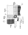
図13及び図14に示されるように、130は、本発明の構成要素たる導電性接触部材である。
As shown in FIGS. 13 and 14,
厚さ約0.05[mm]の銅箔にカーボン含有の導電性を有する粘着剤を塗布したところの接触テープであり、一端の粘着面がRP1上の独立配線引き出し部108の表面に固着し、もう一端の粘着面がFP11上に貼られた後述の導電性を有する前面フィルム142と固着している。
This is a contact tape obtained by applying a carbon-containing conductive adhesive to a copper foil having a thickness of about 0.05 [mm], and the adhesive surface at one end is fixed to the surface of the independent wiring lead-out
131は画像表示部の表示範囲外を囲み、内部への異物の侵入を防ぎ、前記真空容器を前面側から支持するための前フレームであり、アルミニウムやマグネシウムなどの軽金属を押出し加工して成形後、所定の長さに切断し、ねじ止めによって略長方形の額縁を構成している。また、電源部のアースと電気的に接続されている。 131 is a front frame that surrounds the outside of the display range of the image display unit, prevents intrusion of foreign matter into the interior, and supports the vacuum vessel from the front side. After molding by extruding a light metal such as aluminum or magnesium The frame is cut into a predetermined length, and a substantially rectangular frame is formed by screwing. Further, it is electrically connected to the ground of the power supply unit.
134はウレタン発泡樹脂やシリコン発泡樹脂などの弾性材料からなり、接続部材としての接触針135を中央部分で支持するために、接触針135と一体的に成形される前面弾性体である。
A front
また、中フレーム92を設けており、前フレーム131とともに真空容器を挟んで支持する構成としている。中フレームに関しては図9と同じ構成であり、図14では省略している。
In addition, an
また、該前面弾性体134は真空容器のFP11を外フレーム131によって挟み支持する際の緩衝を目的の一つとし、FP11の4辺全周を覆う額縁形状を成している。
Further, the front
135は前述の通り前面弾性体134に支持されて列状に配置された接触針であり、金メッキ処理をした真鍮やステンレスなどの金属ワイヤーを素材としている。
As described above,
該接触針135の一端は前フレーム131に接触し、もう一端はFP11の表面に貼られた導電性を有する前面フィルム142と接触している。142は前述の通りFP11の表面に貼られた導電性を有する前面フィルムであり、PET樹脂を基材としてFP11側にアクリル系粘着剤をコーティング塗布し、表面部前面側にはITO層をスパッタ法で積層している。
One end of the
以上の構成における詳細を説明する。真空容器を構成するRP1上の独立配線引き出し部108にアース電位を供給するための接地構成は、独立配線引き出し部108に接着された接触テープ130、該接触テープ130に接着された前面フィルム142のITO層、該ITO層に接触する接触針135、該接触針135が接触する前フレーム131から構成される。前フレーム131が電源部のアース端子に接地されており、前記接地構造を介して独立配線引き出し部にアース電位が供給される。
Details of the above configuration will be described. The grounding configuration for supplying the ground potential to the independent wiring lead-out
尚、接触テープ130はハサミやカッターで簡単に切断し手作業で任意の位置に接着可能である。
The
また、接触針135は前フレーム131の内壁部と前面フィルム142のITO層表面との距離よりも、約15%長くして電気的接触を確実にしている。そのため接触針135は撓んだ状態で組み込まれるが、接触針135の列の両側から前面弾性体134が挟み支持しているため、倒れたり塑性変形を起こすことも無い。
The
また、本参考例においては真空容器前面を導電性を有する前面フィルム142で覆い、更に真空容器前面周辺を覆う導電性を有する前フレーム131との間でアース電位で接続した。
Further, in this reference example, the front surface of the vacuum vessel was covered with a conductive
そのため、仮に本画像表示装置内部の電気回路などから不要電磁波を発生しても、前記前フレーム131と前面フィルム142のアース電位の略密閉構造により電磁波レベルの減衰が可能となる。
Therefore, even if unnecessary electromagnetic waves are generated from an electric circuit or the like inside the image display device, the electromagnetic wave level can be attenuated by the substantially sealed structure of the ground potential of the
もちろんこの場合は、画像表示装置の背面部にもアース接地した背面カバーを設けて、前フレーム131と電気的に接続するなどにより、背面側の電磁波レベルの減衰を図るのが望ましい。
Of course, in this case, it is desirable to provide a back cover grounded to the back of the image display device and to electrically connect the
以上説明したように、本参考例では、異常放電を抑制する構成と実現するとともに、X,Y方向ドライバー回路のアースパターンに接地するX,Y方向FPCのアース配線と独
立配線105を接続し、更に電源部のアースに接地した前フレーム131に電気的接続する接触針、該接触針に接触する前面フィルムの導電層、該導電層に接触する導電性の接触テープ130を用い、該接触テープ130に独立配線引き出し部108を接触させる構造として、独立配線の電位の規定を確実にした。
As described above, this reference example realizes a configuration that suppresses abnormal discharge, and connects the X and Y direction FPC ground wiring and the
また、前記接触針135は前面弾性体に支持されて前フレーム131に嵌め込む構造としている。
The
接触針135は前フレームに支持されているため、真空容器を前フレームに組み込むことにより半田付けなどの配線作業もせずに前面フィルム142の導電層と前フレームおよび接触針とを電気的に接続することができる。また、前記接触テープ130は道具も使わず手作業で簡単に前面フィルム142の導電層と独立配線引き出し部108を接続できる。
Since the
また、前記接触針135は前面弾性体に支持され、かつ真空容器組み込み後は常に前面フィルム142の導電層を押し付けるため、環境温度の変化や経年変化が有っても電気的接続が保たれる。
Further, the
また、更に画像表示部は、表面側の前フレーム131と背面側の中フレーム92とで弾性を有する前面弾性体134と背面弾性体93を介して挟み支持されているため、外部からの機械的負荷から画像表示部が保護される。
Further, the image display unit is sandwiched and supported between the
また、独立配線にアース電位を供給する構造の一部として、真空容器前面部を前面フィルム142と前フレーム131を用いており、前面フィルム142と前フレーム131もアース接地するため、画像表示部や電気回路からの不要電磁波の漏洩を低減できる。
In addition, as a part of the structure for supplying the ground potential to the independent wiring, the
独立破線へのアース電位の供給に伴い不要電磁波漏洩低減構造へのアース電位の供給ができる構成となっており、異常放電抑制とともに、低コストでの不要電磁波の漏洩対策か施せる。 Along with the supply of the ground potential to the independent broken line, the ground potential can be supplied to the structure for reducing unnecessary electromagnetic wave leakage, so that abnormal discharge can be suppressed and the leakage of unnecessary electromagnetic waves can be implemented at low cost.
(第2の実施形態)
ここでは、薄型平面型の画像表示パネルに電子放出素子を用いたディスプレイを採用し、高圧電源から真空容器内部のフェースプレートの加速電極までの高電位を印加する経路において、RP側の真空容器内の導入線の周囲に高抵抗膜による耐圧構造とリング状のアース電位の独立配線(第1配線)を構成したのはこれまでの参考例と同じである。
(Second Embodiment)
Here, a display using an electron-emitting device is employed in a thin flat type image display panel, and in a path for applying a high potential from a high voltage power source to an acceleration electrode of a face plate inside the vacuum vessel, the inside of the vacuum vessel on the RP side In the same way as the reference examples thus far, a withstand voltage structure by a high resistance film and a ring-shaped independent wiring (first wiring) of the ground potential are formed around the lead-in line.
本実施形態は、FPの真空容器内の画像形成部(加速電極)の周囲に、加速電極とは離間して独立配線(第2配線)を形成した。 In the present embodiment, an independent wiring (second wiring) is formed around the image forming portion (acceleration electrode) in the FP vacuum container so as to be separated from the acceleration electrode.
ここでは、略長方形の加速電極の形状に合わせて、略長方形の加速電極に対して一定の間隔を開けて、加速電極を完全に取り囲むアース電位の独立配線を構成した。 Here, in accordance with the shape of the substantially rectangular acceleration electrode, an independent wiring having a ground potential that completely surrounds the acceleration electrode is configured with a certain interval from the substantially rectangular acceleration electrode.
ここで、両独立配線(第1配線、第2配線)のアース電位の規定を確実にするため、ドライバー回路のアース電位に接地するFPCのアース配線とRP独立配線を接続し、更にRP独立配線の一部を真空容器外に引き出した部分、及び、FP独立配線の一部を真空容器外に引き出した部分の両方に接触して電位供給し、かつ電源部のアースに接地したフレームと電気的に接続するために前フレームの内壁に接触する導電性接触部材を配置した。接触部材はねじ等の固定手段無しにFPとRPの隙間に挿入固定する構成とした。 Here, in order to ensure the specification of the ground potential of both independent wirings (first wiring and second wiring), the FPC ground wiring and the RP independent wiring that are grounded to the ground potential of the driver circuit are connected, and further the RP independent wiring. The frame is electrically connected to the part that is partly pulled out of the vacuum vessel and the part that is part of the FP independent wiring is drawn out of the vacuum vessel and is grounded to the ground of the power supply unit. A conductive contact member that contacts the inner wall of the front frame is disposed for connection to the frame. The contact member was configured to be inserted and fixed in the gap between FP and RP without a fixing means such as a screw.
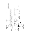
以下に、本発明に係る画像表示装置の第2の実施形態について図15及び図16を参照
して説明する。
Hereinafter, a second embodiment of the image display apparatus according to the present invention will be described with reference to FIGS. 15 and 16.
図15は、本発明に係る画像表示装置の第2の実施形態を表わす画像表示部の角部外観図、図16は、図15に示される画像表示装置の画像表示部の角部断面図である。 FIG. 15 is a corner external view of an image display unit representing a second embodiment of the image display device according to the present invention, and FIG. 16 is a corner cross-sectional view of the image display unit of the image display device shown in FIG. is there.
50は本実施形態の画像表示パネルの真空容器を構成するFP11のRP1側表面に、Agペーストを所定の形状に印刷し、焼成することにより形成したFP独立配線(第2配線)であり、50aは該FP独立配線50の真空部9において、画像形成部12(加速電極)を取り囲むように略長方形を成す配線形状を構成するFP独立配線真空部であり、高電位が印加される前記画像形成部12や高圧引き出し配線100に対して約5mmの沿面距離をあけて配置されている。
50bは前記FP独立配線真空部50aの角部から枠4とFP11の接合部を通過して真空部9外に引き出されたFP独立配線引き出し部であり、前記枠4とFP11の接合部では例えば低融点ガラスに埋設されて外部に引き出されており、真空部9の真空気密を維持できるようになっている。
51は金属製薄板を図示のようにプレス加工により形成した、本発明の構成要素たる導電性接触部材である弾性を有する金属としての接触材であり、該接触材51の先端部にある接触部51aにおいて前記FP独立配線引き出し部50bに電気的機械的に接触している。51bは接触材51のバネ部であり、前記接触部51aをFP独立配線引き出し部50bに押し付けるための弾性を有する形状を成している。
51cは接触部51aとは反対側の端部である接触部であり、前フレーム96の内壁に電気的機械的に接触している。
51 c is a contact portion which is an end portion on the opposite side to the
51dは接触材51のバネ部であり、前記接触部51cを前フレーム96に押し付けるための弾性を有する形状を成している。51eはRP1の2辺にまたがり断面コの字型を成してRP1を挟むところの位置決め部である。
51fは接触材51の中央部付近に複数配置されたエンボス部であり、図15に見える円形は球状の一部を成す凹部で、裏側には該凹部に応じた凸部が形成されて独立配線引き出し部108と電気的機械的に接触している。
該エンボス部51fはバネ部51bとバネ部51dの弾性によって、常に独立配線引き出し部108に押し付け力が働く構造となっている。
The embossed
以上の構成における特徴を述べる。前フレーム96は導電性を有し電源部のアースと電気的に接続している。したがって前フレーム96に接触する接触材51はアース電位となる。更に接触材51と接触するRP1の独立配線引き出し部108およびFP11のFP独立配線50もアース電位となる。
The characteristics of the above configuration will be described. The
その結果、RP1の真空部9においては前述に説明した通り、アース電位の独立配線105、耐圧構造106の構成により、異常放電を抑制でき、電子源領域2に大電流が流れて表面伝導型電子放出素子が劣化したり破壊することを防止することができる。
As a result, in the
更に本実施形態においてはFP11の真空部9においてアース電位の独立配線50aが高電圧が印加される画像形成部12や高圧引き出し配線100を囲む構造としたため、異常放電を抑制でき、異常放電によりFP11から電子源領域2に大電流が流れて表面伝導型電子放出素子が劣化したり破壊することが防止することができる。
Further, in the present embodiment, since the ground potential
また、本実施形態の接触材51の組立は、まず画像表示パネルを構成する真空容器の角部のRP1とFP11の隙間に接触部aを差し込み、次に2個所の位置決め部51eがRP1の2辺の端面に突き当てることで装着が完了する。その後、図16に示す位置に前フレーム96に対して画像表示パネルを組み込むと、接触材51の接触部51cが前フレーム96の内壁に接触する。
Also, in assembling the
更に該真空容器を前述に説明したように、背面側のフレームで弾性体を介して挟み支持するか接着手段により筐体フレームに支持して固定する。 Further, as described above, the vacuum vessel is sandwiched and supported by the frame on the back side via an elastic body, or is supported and fixed to the housing frame by an adhesive means.
以上説明したように、本実施形態では加速電位の供給経路の電子源基板側の経由部における異常放電を抑制できるのみでなく、加速電極に端を発する異常放電による影響をも好適に抑制することができる。 As described above, in this embodiment, not only the abnormal discharge at the transit portion on the electron source substrate side of the supply path of the acceleration potential can be suppressed, but also the influence of the abnormal discharge originating from the acceleration electrode is preferably suppressed. Can do.
また、RP1においてはX,Y方向ドライバー回路のアースパターンに接地するX,Y方向FPC401−X,401−Yのアース配線と独立配線105を接続し、更に独立配線105からの引き出し部を真空容器外に露出させ、FP11においても独立配線50aからのFP独立配線引き出し部50bを真空容器外に露出させ、電源部のアースに接地した前フレーム96に接触する接触材51と両独立配線からの引き出し部を接触させる構造とした。
In RP1, the X and Y direction FPCs 401-X and 401-Y are grounded to the ground pattern of the X and Y direction driver circuit, and the
これにより前記FP11とRP1の独立配線のアース電位の規定を確実にすることができる。 As a result, the ground potential of the independent wiring of the FP11 and RP1 can be ensured.
また、真空容器に固定された前記接触材51はばね性と突き当て部を有しているため、前記FP11とRP1のFP独立配線引き出し部50bおよび独立配線引き出し部108および前フレーム96の内壁を常に押し付けつつ外れることも無い。
Further, since the
半田付けなどの配線作業もせずに電気的に接続されるし、ねじ等の固定手段無しに組み立てられ、環境温度の変化や経年変化が有っても電気的接続が保たれる。 It is electrically connected without wiring work such as soldering, and is assembled without fixing means such as screws, so that the electrical connection is maintained even when there is a change in environmental temperature or aging.
また、前記アース接地構造は、真空容器を前後のフレームで挟み支持したり、RP1を筐体フレームに接着支持したり、様々な支持方法に対応可能であるため、設計の自由度が増す。 In addition, since the grounding structure can support various support methods such as sandwiching and supporting the vacuum vessel between the front and rear frames, and bonding and supporting the RP1 to the housing frame, the degree of freedom in design increases.
ここで、上記第2の参考例、第3の参考例及び第2の実施形態において用いられた接触子、接触板若しくは接触材の材料としては、ステンレスやメッキ処理(防錆処理)リン青銅などが好ましいが、例えばその他にも、リン青銅、鋼、メッキ処理(防錆処理)鋼であっても良い。 Here, as a material of the contactor, the contact plate, or the contact material used in the second reference example, the third reference example, and the second embodiment, stainless steel, plating treatment (rust prevention treatment) phosphor bronze, etc. However, for example, phosphor bronze, steel, or plated (rust-proof) steel may be used.
また、各実施形態の前フレーム96,131は押し出し加工により形成されるものを好適に採用でき、また、前フレーム96,131の材質としては、例えば銅、ニッケル若しくはカーボン等を含有する導電層を有する樹脂製のカバーであっても良い。 In addition, the front frames 96 and 131 of each embodiment can be suitably adopted that formed by extrusion, and the material of the front frames 96 and 131 is, for example, a conductive layer containing copper, nickel, carbon, or the like. It may be a resin cover.
1 リアプレート(RP)
2 電子源領域
3−1 X駆動用配線引き出し部
3−2 Y駆動用配線引き出し部
4 枠
9 真空部
11 フェースプレート(FP)
12 画像形成部
13 気密導入端子
50 FP独立配線
50a 独立配線
50b FP独立配線引き出し部
51 接触材
51a 接触部
51b バネ部
51c 接触部
51d バネ部
51e 位置決め部
51f エンボス部
81 前面フィルム
90 ドライバー回路
91 前面弾性体
92 中フレーム
93 後面弾性体
96 前フレーム
97 接触子
97a 接触子の接触部
97b 接触子のばね部
97c 接触子の固定穴
98 ねじ
100 高圧引き出し配線
105 独立配線
106 耐圧構造
108 独立配線引き出し部
130 接触テープ
131 前フレーム
135 接触針
142 前面フィルム
401−X X方向FPC
401−Y Y方向FPC
1100 接触板
1100a 接触板の先端部
1100b 接触板の接触部
1100c 接触板のバネ部
1100d 接触板の端子部
1101 アースケーブル
1102 端子
1103 ねじ
1700 フェースプレート
1701 ファンネル
1702 テンションバンド
1703 取付け耳部
1704 低抵抗膜
1705 アースケーブル
1706 アース
1707 高圧印加部
1708 高圧ケーブル
1709 電子銃部
1 Rear plate (RP)
2 Electron source region 3-1 X drive wiring lead-out part 3-2 Y drive wiring lead-out
DESCRIPTION OF
401-Y Y direction FPC
1100
Claims (27)
電子放出素子と、
該電子放出素子に接続される駆動配線と、
前記電子放出素子と前記駆動配線が配置される電子源基板と、
前記電子源基板に対向する位置に設けられ、前記電子放出素子が放出する電子を加速する加速電位が与えられる加速電極と、
前記加速電極に前記加速電位を与えるための経路であって、前記電子源基板側の経由部を経由して導出される電位供給経路と、
前記駆動配線とは別に設けられる第1配線であって、前記経由部と前記駆動配線との間の沿面上に設けられる第1配線と、
該第1配線と前記経由部の間の沿面上に設けられる周期的な凹凸構造と、
を有することを特徴とする電子線装置。 An electron beam device,
An electron-emitting device;
Drive wiring connected to the electron-emitting device;
An electron source substrate on which the electron-emitting device and the drive wiring are disposed;
An accelerating electrode provided at a position facing the electron source substrate and applied with an accelerating potential for accelerating electrons emitted from the electron-emitting device;
A path for applying the accelerating potential to the accelerating electrode, and a potential supply path that is derived via a transit part on the electron source substrate side;
A first wiring provided separately from the drive wiring, the first wiring provided on a creeping surface between the transit portion and the drive wiring;
A periodic concavo-convex structure provided on a creeping surface between the first wiring and the transit portion;
An electron beam apparatus comprising:
電子放出素子と、
該電子放出素子に接続される駆動配線と、
前記電子放出素子と前記駆動配線が配置される電子源基板と、
前記電子源基板に対向する位置に設けられ、前記電子放出素子が放出する電子を加速する加速電位が与えられる加速電極と、
前記加速電極に前記加速電位を与えるための経路であって、前記電子源基板を貫通して導出される電位供給経路と、
前記駆動配線とは別に設けられる第1配線であって、前記経由部と前記駆動配線との間の沿面上に設けられる第1配線と、
前記電位供給経路と一体化されており、前記電子源基板に設けられた孔に気密に装着される封止構造と、
該封止構造と前記第1配線の間の沿面上に設けられる凹凸構造と、
を有することを特徴とする電子線装置。 An electron beam device,
An electron-emitting device;
Drive wiring connected to the electron-emitting device;
An electron source substrate on which the electron-emitting device and the drive wiring are disposed;
An accelerating electrode provided at a position facing the electron source substrate and applied with an accelerating potential for accelerating electrons emitted from the electron-emitting device;
A path for applying the accelerating potential to the accelerating electrode, the potential supplying path being led through the electron source substrate;
A first wiring provided separately from the drive wiring, the first wiring provided on a creeping surface between the transit portion and the drive wiring;
A sealing structure integrated with the potential supply path and hermetically mounted in a hole provided in the electron source substrate;
An uneven structure provided on a creeping surface between the sealing structure and the first wiring;
An electron beam apparatus comprising:
方に電気的に接続する請求項4乃至7いずれかに記載の電子線装置。 A second wiring different from the acceleration electrode is provided on the acceleration electrode substrate on which the acceleration electrode is provided, and the conductive contact member is provided on both the leading portion of the first wiring and the leading portion of the second wiring. The electron beam apparatus according to claim 4, wherein the electron beam apparatus is electrically connected.
電子放出素子と、
該電子放出素子に接続される駆動配線と、
前記電子放出素子と前記駆動配線が配置される電子源基板と、
該電子源基板と対向して設けられる加速電極基板と、
該加速電極基板に設けられ、前記電子放出素子が放出する電子を加速する電位が与えられる加速電極と、
該加速電極に前記加速電位を与えるための経路であって、前記電子源基板側の経由部を経由して導出される電位供給経路と、
前記駆動配線とは別に設けられる第1配線であって、前記経由部と前記駆動配線との間の沿面上に設けられる第1配線と、
加速電極基板上の前記加速電極の周囲に前記加速電極とは別に設けられる第2配線と、を有しており、
前記電子源基板と前記加速電極基板の間でかつ周辺枠部で囲まれる空間は真空雰囲気に維持されており、前記第1配線の引き出し部が前記真空雰囲気外に導出されており、かつ、前記第2配線の引き出し部が前記真空雰囲気外に導出されており、導電性接触部材が前記第1配線の前記引き出し部と前記第2配線の前記引き出し部とに接触していることを特徴とする電子線装置。 An electron beam device,
An electron-emitting device;
Drive wiring connected to the electron-emitting device;
An electron source substrate on which the electron-emitting device and the drive wiring are disposed;
An acceleration electrode substrate provided facing the electron source substrate;
An acceleration electrode provided on the acceleration electrode substrate, to which a potential for accelerating electrons emitted from the electron-emitting device is applied;
A path for applying the accelerating potential to the accelerating electrode, the potential supply path being led out via a transit part on the electron source substrate side;
A first wiring provided separately from the drive wiring, the first wiring provided on a creeping surface between the transit portion and the drive wiring;
A second wiring provided separately from the acceleration electrode around the acceleration electrode on the acceleration electrode substrate;
A space between the electron source substrate and the accelerating electrode substrate and surrounded by a peripheral frame is maintained in a vacuum atmosphere, a lead-out portion of the first wiring is led out of the vacuum atmosphere, and The lead portion of the second wiring is led out of the vacuum atmosphere, and the conductive contact member is in contact with the lead portion of the first wire and the lead portion of the second wire. Electron beam equipment.
Priority Applications (1)
| Application Number | Priority Date | Filing Date | Title |
|---|---|---|---|
| JP2005123607A JP2005222958A (en) | 2000-07-24 | 2005-04-21 | Electron beam device and image display device |
Applications Claiming Priority (3)
| Application Number | Priority Date | Filing Date | Title |
|---|---|---|---|
| JP2000222936 | 2000-07-24 | ||
| JP2001212033 | 2001-07-12 | ||
| JP2005123607A JP2005222958A (en) | 2000-07-24 | 2005-04-21 | Electron beam device and image display device |
Related Parent Applications (1)
| Application Number | Title | Priority Date | Filing Date |
|---|---|---|---|
| JP2001218314A Division JP3689651B2 (en) | 2000-07-24 | 2001-07-18 | Electron beam equipment |
Related Child Applications (1)
| Application Number | Title | Priority Date | Filing Date |
|---|---|---|---|
| JP2006110894A Division JP2006222093A (en) | 2000-07-24 | 2006-04-13 | Electron beam device and image display device |
Publications (2)
| Publication Number | Publication Date |
|---|---|
| JP2005222958A true JP2005222958A (en) | 2005-08-18 |
| JP2005222958A5 JP2005222958A5 (en) | 2006-06-15 |
Family
ID=34998388
Family Applications (1)
| Application Number | Title | Priority Date | Filing Date |
|---|---|---|---|
| JP2005123607A Withdrawn JP2005222958A (en) | 2000-07-24 | 2005-04-21 | Electron beam device and image display device |
Country Status (1)
| Country | Link |
|---|---|
| JP (1) | JP2005222958A (en) |
Cited By (1)
| Publication number | Priority date | Publication date | Assignee | Title |
|---|---|---|---|---|
| JP2010151852A (en) * | 2008-12-23 | 2010-07-08 | Nippon Seiki Co Ltd | Liquid crystal display |
-
2005
- 2005-04-21 JP JP2005123607A patent/JP2005222958A/en not_active Withdrawn
Cited By (1)
| Publication number | Priority date | Publication date | Assignee | Title |
|---|---|---|---|---|
| JP2010151852A (en) * | 2008-12-23 | 2010-07-08 | Nippon Seiki Co Ltd | Liquid crystal display |
Similar Documents
| Publication | Publication Date | Title |
|---|---|---|
| JP3689651B2 (en) | Electron beam equipment | |
| EP0866490B1 (en) | Image-forming apparatus | |
| JP3768718B2 (en) | Image forming apparatus | |
| KR100450627B1 (en) | Image displaying apparatus | |
| JP4250608B2 (en) | Image display device and manufacturing method thereof | |
| JP3848240B2 (en) | Image display device | |
| JP3944211B2 (en) | Image display device | |
| JP3984942B2 (en) | Image display device and information display device | |
| JP3478727B2 (en) | Image forming device | |
| JP2006222093A (en) | Electron beam device and image display device | |
| JP2011129487A (en) | Display apparatus | |
| JP2005222958A (en) | Electron beam device and image display device | |
| EP1347489B1 (en) | High voltage type image display apparatus | |
| JP4103679B2 (en) | Display device | |
| JP2007109603A (en) | Image display device | |
| US8089204B2 (en) | Display panel, display and image display apparatus | |
| JP3478774B2 (en) | Image display device | |
| JP2005235740A (en) | Manufacturing method of airtight container, manufacturing method of picture display device, and manufacturing method of tv apparatus | |
| US8040037B2 (en) | Image display apparatus | |
| JP2010262778A (en) | Display panel, display device, television apparatus, and method of manufacturing the display panel | |
| JP3768876B2 (en) | Display device | |
| JP2004087474A (en) | Image display, and its manufacturing method | |
| JP2011243497A (en) | Image display device | |
| JP2003249183A (en) | Image forming device | |
| JP2000251770A (en) | Airtight container and image forming device |
Legal Events
| Date | Code | Title | Description |
|---|---|---|---|
| A521 | Written amendment |
Free format text: JAPANESE INTERMEDIATE CODE: A523 Effective date: 20060413 |
|
| A977 | Report on retrieval |
Free format text: JAPANESE INTERMEDIATE CODE: A971007 Effective date: 20060613 |
|
| A131 | Notification of reasons for refusal |
Free format text: JAPANESE INTERMEDIATE CODE: A131 Effective date: 20060704 |
|
| A761 | Written withdrawal of application |
Free format text: JAPANESE INTERMEDIATE CODE: A761 Effective date: 20060710 |