JP3763258B2 - Probe card and chip area sorting method using the same - Google Patents
Probe card and chip area sorting method using the same Download PDFInfo
- Publication number
- JP3763258B2 JP3763258B2 JP2000321204A JP2000321204A JP3763258B2 JP 3763258 B2 JP3763258 B2 JP 3763258B2 JP 2000321204 A JP2000321204 A JP 2000321204A JP 2000321204 A JP2000321204 A JP 2000321204A JP 3763258 B2 JP3763258 B2 JP 3763258B2
- Authority
- JP
- Japan
- Prior art keywords
- chip
- regions
- opposing
- probe card
- region
- Prior art date
- Legal status (The legal status is an assumption and is not a legal conclusion. Google has not performed a legal analysis and makes no representation as to the accuracy of the status listed.)
- Expired - Fee Related
Links
Images


Description
【0001】
【発明の属する技術分野】
本発明は、ウェハ状態におけるLSIチップのパッドに探針を機械的に接触させて電気的特性を測定するプローブカード及びそれを用いたチップ領域ソート方法に関する。
【0002】
【従来の技術】
プローブカードは、LSI製造の組立工程前におけるウェハ状態での試験に用いられるものである。プローブカードは、被測定LSIチップ領域のボンディングパッドそれぞれに対応して接触させる探針を有する。この探針からLSIチップに試験信号または試験パターンを入力する。
【0003】
プローブカードは、テスタに接続されテストシステムを構築する一部となる。テスタは、プローブカードを介し、LSIからの出力値を期待値と比較してLSIの機能の良否を判定したり、入出力信号、電源部分の電圧、電流などのアナログ値等の測定をする。このようなウェハプロービング試験を経て良品として選別されたLSIが組立工程へと回される。
【0004】
近年、ウェハの大口径化が進み、ウェハあたりのチップ取得数も多くなる傾向にある。これに伴い、上記のようなウェハプロービング試験に費やされる時間が増大し、高効率化が望まれている。
【0005】
そこで、可能な限り複数個のチップを同時に試験できるように、複数個取りのプローブカードが使用されるようになってきた。特にセンターパッド方式のLSIチップや、パッド数が比較的少ないタイプのLSIチップに対して複数個取りのプローブカードが使用される。
【0006】
【発明が解決しようとする課題】
LSIチップの多様化は著しく、データの入出力数は多くなっている。これに伴いチップ1個あたりのパッド数は増大し、チップ周囲に狭いピッチで配列されるものも少なくない。こうなると、プローブカードの各探針を全パッド(あるいはバンプ)それぞれに当てることが困難になってくる。
【0007】
プローブカードの各探針について伸長元を多層にする工夫は一般に知られている技術である。これにより、例えば接触領域(パッド、バンプ等)の配列ピッチが探針線材径(母材径)より小さい場合でも各探針の接触は可能になる。
【0008】
しかしながら、接触領域(パッド、バンプ等)のさらなる狭ピッチ化が進む場合、上記技術だけでは信頼性の懸念は解消され難い。測定対象の各接触領域全てに探針を当てる構成は、測定における探針各々の圧力差、位置ずれが許容できない状態になり易く、隣接間ショートなどの危険性をいっそう増大させる。
【0009】
本発明は上記のような事情を考慮してなされたもので、測定対象となる接触領域(パッド、バンプ等)が狭ピッチの場合に探針配列の密集を軽減しつつ、高信頼性を維持しやすいプローブカード及びそれを用いたチップ領域ソート方法を提供しようとするものである。
【0010】
【課題を解決するための手段】
本発明に係るプローブカードは、ウェハ上で複数の入力端子の配列と前記入力端子より狭ピッチの複数の出力端子の配列とが隣り合う複数のチップ領域に対向させ信号の授受を担う回路基材であって、前記回路基材において前記チップ領域それぞれに対応して設けられた対向接続領域と、前記対向接続領域それぞれに関し、前記チップ領域における前記入力端子全部かつ互いに隣り合う箇所を除いた前記出力端子に対応する位置まで伸び、前記回路基材と前記ウェハを接近させることで前記チップ領域の各端子に接触させる複数の電気的接続部材とを具備し、前記対向接続領域の一つにおける前記電気的接続部材と前記対向接続領域の別の一つにおける前記電気的接続部材とは、接触すべき前記出力端子の互いに隣り合う箇所を補完し合う配置関係にあることを特徴とする。
【0011】
上記本発明に係るプローブカードによれば、複数の入力端子の配列と入力端子より狭ピッチの複数の出力端子の配列とが隣り合っている複数のチップ領域が測定対象となる。チップ領域一つに配された狭ピッチの出力端子について複数回に分けた測定とする。接続を分担すれば、狭ピッチで隣り合う端子への接続をその時点では間引くことができる。これにより、出力端子が著しく狭ピッチの配列である場合にも、より安定した電気的接続部材の接続が可能になる。
【0012】
本発明に係るプローブカードを用いたチップ領域ソート方法は、ウェハ上で複数の入力端子の配列と前記入力端子より狭ピッチの複数の出力端子の配列とが隣り合う複数のチップ領域に対向させ信号の授受を担うプローブカードの各チップ領域へのソートに関し、前記プローブカードは前記チップ領域各々に対応してそれぞれ周縁に電気的接続部材が配列する対向接続領域を有し、前記電気的接続部材は前記対向接続領域それぞれに関し、前記チップ領域における前記入力端子全部かつ互いに隣り合う箇所を除いた前記出力端子に対応する位置まで伸び、前記対向接続領域の一つにおける前記電気的接続部材と前記対向接続領域の別の一つにおける前記電気的接続部材とは、接触すべき前記出力端子の互いに隣り合う箇所を補完し合う配置関係にあって、前記チップ領域における各端子全てに対し前記電気的接続部材の接触が満足されるまでそれぞれ異なる前記対向接続領域を各チップ領域へ接近、接続させるように移動制御されること、を特徴とする。
【0013】
上記本発明に係るプローブカードを用いたチップ領域ソート方法によれば、プローブカードはチップ領域各々に対応してそれぞれ周縁に電気的接続部材が配列する対向接続領域を有する。しかも、電気的接続部材は、対向接続領域それぞれに関し、チップ領域における入力端子全部かつ互いに隣り合う箇所を除いた出力端子に対応する位置まで伸び、対向接続領域の一つにおける電気的接続部材と対向接続領域の別の一つにおける電気的接続部材とは、接触すべき出力端子の互いに隣り合う箇所を補完し合う配置関係にある。これにより、各対向接続領域で設けられる電気的接続部材で役割が分担され、各対向接続領域のチップ領域への対向、接近(接続)によって、一つのチップ領域における端子部全てと電気的接続部材の接触が満足されるようにする。これにより、チップ領域における狭ピッチの出力端子それぞれに対し、電気的接続部材の当る確度を高める。
【0014】
【発明の実施の形態】
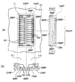
図1(a),(b)は、それぞれ本発明の第1実施形態に係るプローブカードの要部構成を示しており、(a)は上面からの概観図、(b)は横からの任意の断面を示す概略図である。
【0015】
プローブカードを構成する回路基材10は、ウェハWF上の複数のチップ領域CHIPに対向させて信号の授受を担うものである。回路基材10は、例えば図示しないテストヘッドに繋がるプローバに装着される。ウェハWF及びチップ領域CHIPは破線で示されている。
【0016】
チップ領域CHIPには外部端子、ここではバンプ電極BMPが設けられている。このチップ領域CHIPは、例えば入力端子の配列DINと、出力端子の配列DOUTが区分されており、入力端子の配列DINに比べ出力端子の配列DOUT側が狭ピッチのバンプ配列となっている。
【0017】
回路基材10には開口部11が設けられている。この開口部11にはチップ領域CHIPに応じた対向接続領域111,112が設けられている。これら対向接続領域111,112それぞれに関し、開口部11の周縁部からチップ領域CHIPにおける所定の外部端子(ここではバンプ電極BMP)の位置まで伸びる探針101,102が設けられている。図1(b)に示すように、探針101,102の伸長元は多層(ここでは2層)になる部分を有する。これら探針101,102は、回路基材10とウェハWFを接近させることで測定対象のチップ領域CHIPにおける所定のバンプ電極BMPに接触させる構成となっている。
【0018】
この実施形態において、対向接続領域111における探針101と対向接続領域112における探針102は、バンプ電極BMPが狭ピッチで配列された出力端子の配列DOUTに対応する領域において、配置が異なっている。図1(a)に示すように探針101と102は、チップ領域CHIPの出力端子の配列DOUTに対応する領域で、互いに隣り合うバンプ電極BMPを除いて対応するように配設されている。
【0019】
すなわち、探針101と探針102とは、出力端子側のバンプ電極BMP群に対応する領域に関し、隣り合う接触を補完し合う配置関係にある。なお、比較的狭ピッチとならない入力端子の配列DIN側のバンプ電極BMP群については、測定時は常に全バンプ探針が接触される。すなわち、探針101と102において、入力端子の配列DIN側に対応する領域については同じ配列である。
【0020】
これにより、一つのチップ領域CHIPについて、対向接続領域111及び112をそれぞれ対向、接近させることで、チップ領域CHIPにおけるバンプ電極BMP群全てについて探針の接触、電気的特性試験が満足される。すなわち、非常に狭ピッチで、測定を分けても支障のない出力系のバンプ配列の探針接触について適用されたものである。
【0021】
上記実施形態の構成によれば、測定箇所を対向接続領域111における探針101と対向接続領域112における探針102とで分担する。これにより、接触すべき端子部が著しく狭ピッチの配列である場合に有効である。
【0022】
すなわち、本発明によれば、狭ピッチの端子配列に全て1対1で対応させるような探針のレイアウトを必ずしも必要としない技術が提供できるといえる。この結果、プローブカードは、測定において探針各々の圧力差、位置ずれが許容できない状態には極めてなり難く、かつ、隣接間ショートなどの危険性を回避しやすい構成を実現することができる。
【0023】
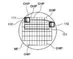
図2は、図1の構成のプローブカードを用いたチップ領域ソート方法の一例を示す概略図である。ウェハWFのチップ領域CHIP毎に配された図示しない複数の端子部に対し測定対象とする接続を分担しつつソートする。
【0024】
すなわち、チップ領域CHIP一つにおける図示しない端子部全てに対し探針(101,102)の接触が満足されるまでそれぞれ異なる対向接続領域111,112を各チップ領域CHIPへ接近、接続させるように移動制御する。
【0025】
図2において、各チップ領域CHIPは、方向Rでは対向接続領域112→111の順により、方向Lでは対向接続領域111→112の測定順により、各チップ領域CHIPの端子部に対し全ての探針(101,102)の接触が順次満足される。
【0026】
上記実施形態のプローブカードを用いたチップ領域ソート方法によれば、測定の分担化により測定対象とする接続に余裕を持たせることができる。すなわち、幾つかの対向接続領域(ここでは111,112の二つ)の対向、接近(接続)によって、各チップ領域における端子部全てについて、確度の高い探針の接触が実現される。
【0027】
なお、上記対向接続領域111,112のセットは複数設けてもよい。これにより、同時側定数の向上が望める。また、対向接続領域111,112のレイアウトは他にも考えられる。また、上記実施形態では対向接続領域111,112を一つの開口部11内に設けたプローブカードの構成を示したが、対向接続領域111,112それぞれを別々の開口部で構成するプローブカードであってもよい。
【0028】
図3は、本発明の第2実施形態に係るプローブカードの要部構成を示す概観図である。上記第1実施形態の構成に比べて対向接続領域それぞれを別々の開口部で構成している。
【0029】
この実施形態では、プローブカードを構成する回路基材30に設けられた対向接続領域311,312とし、それぞれ上記第1実施形態の対向接続領域111,112と同様の関係にあるものとした。対向接続領域311,312それぞれに関し、その周縁部からチップ領域CHIPにおける所定の外部端子(ここではバンプ電極BMP)の位置まで伸びる探針301,302が設けられている。探針301,302の伸長元は図示しないが単層でも多層でもよく、様々考えられる。
【0030】
その他、測定対象のチップ領域CHIPの端子配列については上記第1実施形態と同様に構成される。これら探針301,302は、回路基材30とウェハWFを対向、接近させることで測定対象のチップ領域CHIPにおける所定のバンプ電極BMPに接触させる構成となっている。
【0031】
この実施形態においても、対向接続領域311における探針301と対向接続領域312における探針302は、バンプ電極BMPが狭ピッチで配列されている出力端子の配列DOUTに対応する領域において、異なった配置を有する。探針301と302は、チップ領域CHIPの出力端子の配列DOUTに対応する領域で、互いに隣り合うバンプ電極BMPを除いて対応するように配設されている。
【0032】
すなわち、探針301と探針302とは、出力端子側のバンプ電極BMP群に対応する領域に関し、隣り合う接触を補完し合う配置関係にある。なお、入力端子の配列DIN側のバンプ電極BMP群については、測定時は常に全バンプ探針が接触される。すなわち、探針301と302において、入力端子の配列DIN側に対応する領域については同じ配列である。
【0033】
これにより、一つのチップ領域CHIPについて、対向接続領域311及び312をそれぞれ対向、接近させることで、チップ領域CHIPにおけるバンプ電極BMP群全てについて探針の接触、測定が満足される。
【0034】
上記実施形態の構成によれば、測定箇所を対向接続領域311における探針301と対向接続領域312における探針302とで分担する。これにより、接触すべき端子部が著しく狭ピッチの配列である場合に有効である。すなわち、狭ピッチの端子配列に全て1対1で対応させるような探針のレイアウトを必ずしも必要としない技術が提供できるといえる。この結果、プローブカードは、測定において探針各々の圧力差、位置ずれが許容できないような状態には極めてなり難く、かつ、隣接間ショートなどの危険性を回避しやすい構成を実現することができる。
【0035】
図4は、図3の構成のプローブカードを用いたチップ領域ソート方法の一例を示す概略図である。ウェハWFのチップ領域CHIP毎に配された図示しない複数の端子部に対し測定対象とする接続を分担しつつソートする。
【0036】
すなわち、チップ領域CHIP一つにおける図示しない端子部全てに対し探針(301,302)の接触が満足されるまでそれぞれ異なる対向接続領域311,312を各チップ領域CHIPへ接近、接続させるように移動制御する。
【0037】
図4において、各チップ領域CHIPは、方向R、L共に対向接続領域311,312のどちらか一方を用いて先に1列分が順次測定され、折り返しソートする際に、他方の対向接続領域(311,312いずれか)を用いて1列分が重複するように順次測定される。これにより、各チップ領域CHIPの端子部において全ての探針(301,302)の接触が満足される。
【0038】
なお、上記対向接続領域311,312のセットは複数設けてもよい。これにより、同時側定数の向上が望める。また、対向接続領域311,312のレイアウトは他にも考えられる。特に回路基材における個々の開口部で対向接続領域を構成する場合、本発明の特徴である探針の間引き構造によってレイアウトの自由度が得られる。
【0039】
図5(a)〜(d)は、それぞれ同時側定数の向上を目的としたプローブカードに関し、ウェハのチップ領域への回路基材における対向接続領域の構成例を示した概略図である。各々対向接続領域には図示しない探針配列が設けられる。
【0040】
図5(a)において、対向接続領域A1とA2は、図示しない探針配列が、ある特定領域において、チップ領域で接触すべき隣り合う端子部に対応する箇所を補完し合う配置関係にある。上記特定領域とは、対応するチップ領域で接触すべき端子部が狭ピッチである領域が挙げられる。また、検査測定の分担に伴ない、接触を間引いても検査測定に支障ないことが重要である。
【0041】
ウェハの各チップ領域に対する検査測定は、同じ探針配列の対向接続領域が並ぶ方向でチップ領域2つ分重複させながら順次ソートされ、達成される。さらに同時測定数を増やしたければ対向接続領域A1とA2のセットを増やせばよい。その際、各対向接続領域のレイアウトは限定されるものではない。
【0042】
図5(b)において、対向接続領域B1とB2は、図示しない探針配列が、ある特定領域において、チップ領域で接触すべき隣り合う端子部に対応する箇所を補完し合う配置関係にある。上記特定領域とは、対応するチップ領域で接触すべき端子部が狭ピッチである領域が挙げられる。また、検査測定の分担に伴ない、接触を間引いても検査測定に支障ないことが重要である。
【0043】
ウェハの各チップ領域に対する検査測定は、同じ探針配列の対向接続領域が並ぶ方向でチップ領域2つ分重複させながら順次ソートされ、達成される。さらに同時測定数を増やしたければ対向接続領域B1とB2のセットを増やせばよい。その際、各対向接続領域のレイアウトは限定されるものではない。
【0044】
図5(c)において、対向接続領域C1とC2は、図示しない探針配列が、ある特定領域において、チップ領域で接触すべき隣り合う端子部に対応する箇所を補完し合う配置関係にある。上記特定領域とは、対応するチップ領域で接触すべき端子部が狭ピッチである領域が挙げられる。また、検査測定の分担に伴ない、接触を間引いても検査測定に支障ないことが重要である。
【0045】
ウェハの各チップ領域に対する検査測定は、同じ探針配列の対向接続領域が並ぶ方向でチップ領域2つ分重複させながら順次ソートされ、達成される。さらに同時測定数を増やしたければ対向接続領域C1とC2のセットを増やせばよい。その際、各対向接続領域のレイアウトは限定されない。
【0046】
図5(d)は、図5(c)の変形例である。同時側定数の向上を目的とした構成で探針の配列に困難性がある場合の構成である。対向接続領域C1とC2のセットをチップ領域1つ分離間させてもう1セット設ける。このようにすれば、探針の配線引き回しに余裕が得られる。このような構成のソートにおいても2重に測定されないよう制御する。前記図5(a)や図5(b)の対向接続領域のセットもこのような工夫が容易に考えられる。
【0047】
さらに、上記各実施形態によれば、一つのチップ領域に対し二つの対向接続領域で電気的測定を分担する構成を示したが、これに限らない。一つのチップ領域に対し二つ以上の多数の対向接続領域で電気的測定を分担する構成を実現してもよい。これにより、個々の対向接続領域における探針配列の精度に関するマージンを大きくすることができる。この結果、プローブカードは、測定において探針各々の圧力差、位置ずれが許容できない状態には極めてなり難く、また隣接間ショートなどの危険性を軽減することができる。
【0048】
以上のような各実施形態におけるプローブカード及びチップ領域のソート方法によれば、プローブカードは探針の密集は許容できる程度に抑えられ、かつ、なるべく多くの同時測定数を確保することも可能となる。また、探針の配列ピッチの縮小化、伸長元の多層化が抑えられるので、メンテナンスも容易になり高信頼性を維持しやすい多数個取りのプローブカードの構成が実現できる。また、ソートにおいて2重に測定されない制御はもちろんのこと、多数個取りにより、ウェハプロービング試験に費やされる時間がより減少し、高効率化が達成できる。
【0049】
【発明の効果】
以上説明したように本発明によれば、プローブカードは、対向させるチップ領域一つに配された複数の端子部に対し測定対象とする接続を分担するようにしたので、探針配列の精度、信頼性への配慮に伴う構成、その負担を軽減することができる。
【0050】
そして、多数個取りの構成を実現すれば、ウェハの大口径化に対してもウェハプロービング試験時間の減少、信頼性を伴った高効率化に寄与する。この結果、修理、メンテナンスも容易で高信頼性を維持しやすい高効率の多数個取りのプローブカード及びを用いたチップ領域ソート方法を提供することができる。
【図面の簡単な説明】
【図1】(a),(b)は、それぞれ本発明の第1実施形態に係るプローブカードの要部構成を示しており、(a)は上面からの概観図、(b)は横からの任意の断面を示す概略図である。
【図2】図1の構成のプローブカードを用いたチップ領域ソート方法の一例を示す概略図である。
【図3】本発明の第2実施形態に係るプローブカードの要部構成を示す概観図である。
【図4】図3の構成のプローブカードを用いたチップ領域ソート方法の一例を示す概略図である。
【図5】(a)〜(d)は、それぞれ同時側定数の向上を目的としたプローブカードに関し、ウェハのチップ領域への回路基材における対向接続領域の構成例を示した概略図である。
【符号の説明】
10,30…回路基材(プローブカード)
11…開口部
111,112,311,312,A1,A2,B1,B2,C1,C2…対向接続領域、
101,102,301,302…探針
BMP…バンプ電極
WF…ウェハ
CHIP…チップ領域
DIN…入力端子の配列
DOUT…出力端子の配列[0001]
BACKGROUND OF THE INVENTION
The present invention relates to a probe card for measuring electrical characteristics by mechanically contacting a probe to a pad of an LSI chip in a wafer state and a chip area sorting method using the same.
[0002]
[Prior art]
The probe card is used for a test in a wafer state before an assembly process of LSI manufacturing. The probe card has a probe to be brought into contact with each bonding pad in the LSI chip area to be measured. A test signal or a test pattern is input from this probe to the LSI chip.
[0003]
The probe card is connected to a tester and becomes a part of building a test system. The tester compares the output value from the LSI with an expected value via the probe card to determine the quality of the LSI, and measures analog values such as input / output signals, power supply voltage, and current. An LSI selected as a non-defective product through such a wafer probing test is sent to an assembly process.
[0004]
In recent years, the diameter of wafers has increased, and the number of chips acquired per wafer tends to increase. Accordingly, the time spent for the wafer probing test as described above is increased, and higher efficiency is desired.
[0005]
Therefore, a plurality of probe cards have been used so that a plurality of chips can be simultaneously tested as much as possible. In particular, a plurality of probe cards are used for a center pad type LSI chip or a type of LSI chip having a relatively small number of pads.
[0006]
[Problems to be solved by the invention]
The diversification of LSI chips is remarkable, and the number of data input / output is increasing. As a result, the number of pads per chip increases, and many pads are arranged at a narrow pitch around the chip. In this case, it becomes difficult to apply each probe of the probe card to each pad (or bump).
[0007]
A technique of making the extension source multilayer for each probe of the probe card is a generally known technique. Thereby, for example, even when the arrangement pitch of the contact areas (pads, bumps, etc.) is smaller than the probe wire diameter (base material diameter), the probes can contact each other.
[0008]
However, when the contact area (pads, bumps, etc.) is further narrowed in pitch, it is difficult to eliminate the concern about reliability only with the above technique. The configuration in which the probe is applied to all the contact areas to be measured tends to be in an unacceptable state of pressure difference and positional deviation of each probe in the measurement, and further increases the risk of short circuit between adjacent points.
[0009]
The present invention has been made in view of the above circumstances, and maintains high reliability while reducing the density of probe arrangements when the contact area (pad, bump, etc.) to be measured has a narrow pitch. It is an object of the present invention to provide a probe card that is easy to perform and a chip area sorting method using the same.
[0010]
[Means for Solving the Problems]
The probe card according to the present invention is a circuit substrate for transferring signals by arranging an array of a plurality of input terminals and an array of a plurality of output terminals having a narrower pitch than the input terminals on a wafer so as to face adjacent chip regions. In the circuit base material, each of the opposing connection regions provided corresponding to each of the chip regions, and each of the opposing connection regions, the output except for all the input terminals in the chip region and adjacent to each other. A plurality of electrical connection members extending to positions corresponding to the terminals and bringing the circuit base material and the wafer into contact with each other to contact each terminal in the chip region, and the electrical connection in one of the opposing connection regions The electrical connection member and the electrical connection member in another one of the opposed connection regions are arranged so as to complement each other of the output terminals to be contacted with each other. Characterized in that a relationship.
[0011]
According to the probe card according to the present invention, a plurality of chip regions in which an array of a plurality of input terminals and an array of a plurality of output terminals having a narrower pitch than the input terminals are adjacent to each other are to be measured. The measurement is divided into a plurality of times for the narrow pitch output terminals arranged in one chip area. If connections are shared, connections to adjacent terminals at a narrow pitch can be thinned out at that time. Thereby, even when the output terminals are arranged in a remarkably narrow pitch, a more stable connection of the electrical connection member is possible.
[0012]
In the chip area sorting method using the probe card according to the present invention, an array of a plurality of input terminals and a plurality of output terminals having a narrower pitch than the input terminals are opposed to a plurality of adjacent chip areas on the wafer. The probe card has an opposing connection region in which an electrical connection member is arranged on the periphery corresponding to each of the chip regions, and the electrical connection member is For each of the opposing connection regions, the electrical connection member and the opposing connection in one of the opposing connection regions extend to a position corresponding to the output terminal except for all the input terminals in the chip region and adjacent to each other. The electrical connection member in another one of the regions is an arrangement relationship that complements adjacent portions of the output terminals to be contacted with each other. Then, the movement control is performed so that the different opposing connection regions are brought close to and connected to the respective chip regions until the contact of the electrical connection member is satisfied with respect to all the terminals in the chip region. And
[0013]
According to the chip area sorting method using the probe card according to the present invention, the probe card has an opposing connection area in which electrical connection members are arranged on the periphery corresponding to each chip area. In addition, the electrical connection member extends to a position corresponding to the output terminals except for all the input terminals in the chip region and the portions adjacent to each other, and faces the electrical connection member in one of the opposing connection regions. The electrical connection member in another one of the connection regions has an arrangement relationship in which the adjacent output terminals to be contacted with each other are complemented. As a result, the electrical connection members provided in each opposing connection region share the role. By facing and approaching (connecting) each opposing connection region to the chip region, all the terminal portions in one chip region and the electrical connection member So that the contact is satisfied. This increases the accuracy with which the electrical connection member hits each of the narrow pitch output terminals in the chip region.
[0014]
DETAILED DESCRIPTION OF THE INVENTION
1 (a) and 1 (b) show the main configuration of the probe card according to the first embodiment of the present invention, respectively (a) is an overview from the top, and (b) is an arbitrary view from the side. It is the schematic which shows the cross section.
[0015]
The
[0016]
The chip region CHIP is provided with external terminals, here bump electrodes BMP. In this chip area CHIP, for example, an input terminal array DIN and an output terminal array DOUT are divided, and the output terminal array DOUT side has a narrower bump array than the input terminal array DIN.
[0017]
An
[0018]
In this embodiment, the arrangement of the
[0019]
That is, the
[0020]
Thus, the probe contact and electrical characteristic tests are satisfied for all the bump electrodes BMP groups in the chip region CHIP by making the opposing
[0021]
According to the configuration of the above embodiment, the measurement location is shared by the
[0022]
That is, according to the present invention, it can be said that it is possible to provide a technique that does not necessarily require the layout of the probe so as to correspond one-to-one to the narrow pitch terminal arrangement. As a result, the probe card is unlikely to be in a state where the pressure difference and positional deviation of each probe cannot be tolerated in measurement, and can realize a configuration that can easily avoid dangers such as a short circuit between adjacent probes.
[0023]
FIG. 2 is a schematic diagram showing an example of a chip area sorting method using the probe card having the configuration shown in FIG. Sorting is performed while sharing the connection to be measured with respect to a plurality of terminal portions (not shown) arranged for each chip region CHIP of the wafer WF.
[0024]
That is, different opposing
[0025]
In FIG. 2, each chip region CHIP has all the probes for the terminal portions of each chip region CHIP in the direction R in the order of the opposing
[0026]
According to the chip area sorting method using the probe card of the above embodiment, it is possible to give a margin to the connection to be measured by sharing the measurement. That is, the probe contact with high accuracy is realized for all the terminal portions in each chip region by facing and approaching (connecting) several facing connection regions (here, two of 111 and 112).
[0027]
Note that a plurality of sets of the opposing
[0028]
FIG. 3 is a schematic view showing a main configuration of a probe card according to the second embodiment of the present invention. Compared to the configuration of the first embodiment, each of the opposing connection regions is configured by a separate opening.
[0029]
In this embodiment, the opposing
[0030]
In addition, the terminal arrangement of the chip region CHIP to be measured is configured in the same manner as in the first embodiment. The
[0031]
Also in this embodiment, the
[0032]
That is, the
[0033]
Thereby, the contact and measurement of the probe are satisfied for all the bump electrodes BMP group in the chip region CHIP by making the opposing
[0034]
According to the configuration of the above embodiment, the measurement location is shared by the
[0035]
FIG. 4 is a schematic diagram showing an example of a chip area sorting method using the probe card having the configuration shown in FIG. Sorting is performed while sharing the connection to be measured with respect to a plurality of terminal portions (not shown) arranged for each chip region CHIP of the wafer WF.
[0036]
That is, the different opposing
[0037]
In FIG. 4, each chip region CHIP is sequentially measured for one column using either one of the opposing
[0038]
Note that a plurality of sets of the
[0039]
FIGS. 5A to 5D are schematic diagrams showing a configuration example of the opposing connection region in the circuit base material to the chip region of the wafer, with respect to the probe card for the purpose of improving the simultaneous side constant, respectively. A probe array (not shown) is provided in each opposing connection region.
[0040]
In FIG. 5A, the opposing connection areas A1 and A2 are in a relationship in which probe arrangements (not shown) complement each other in locations corresponding to adjacent terminal portions to be contacted in the chip area in a specific area. The specific region includes a region where the terminal portions to be contacted in the corresponding chip region have a narrow pitch. Also, with the sharing of inspection measurement, it is important that the inspection measurement is not hindered even if the contact is thinned out.
[0041]
The inspection measurement for each chip area of the wafer is accomplished by sequentially sorting the two chip areas overlapping in the direction in which the opposing connection areas of the same probe array are arranged. To further increase the number of simultaneous measurements, the number of opposing connection areas A1 and A2 may be increased. In that case, the layout of each opposing connection area is not limited.
[0042]
In FIG. 5B, the opposed connection regions B1 and B2 are in a relationship in which a probe array (not shown) complements a portion corresponding to an adjacent terminal portion to be contacted in a chip region in a specific region. The specific region includes a region where the terminal portions to be contacted in the corresponding chip region have a narrow pitch. Also, with the sharing of inspection measurement, it is important that the inspection measurement is not hindered even if the contact is thinned out.
[0043]
The inspection measurement for each chip area of the wafer is accomplished by sequentially sorting the two chip areas overlapping in the direction in which the opposing connection areas of the same probe array are arranged. To further increase the number of simultaneous measurements, the set of opposing connection areas B1 and B2 may be increased. In that case, the layout of each opposing connection area is not limited.
[0044]
In FIG. 5C, the opposed connection regions C1 and C2 are in a relationship in which a probe array (not shown) complements a portion corresponding to an adjacent terminal portion to be contacted in the chip region in a specific region. The specific region includes a region where the terminal portions to be contacted in the corresponding chip region have a narrow pitch. Also, with the sharing of inspection measurement, it is important that the inspection measurement is not hindered even if the contact is thinned out.
[0045]
The inspection measurement for each chip area of the wafer is accomplished by sequentially sorting the two chip areas overlapping in the direction in which the opposing connection areas of the same probe array are arranged. To further increase the number of simultaneous measurements, the set of opposing connection areas C1 and C2 may be increased. In that case, the layout of each opposing connection area is not limited.
[0046]
FIG.5 (d) is a modification of FIG.5 (c). This is a configuration for the purpose of improving the simultaneous constant and is a configuration in the case where there is a difficulty in arranging the probes. Another set of opposing connection areas C1 and C2 is provided with one chip area separated. In this way, a margin can be obtained for the wiring of the probe. Control is also performed so as not to measure twice even in such a sort. Such a device can be easily considered for the set of opposed connection regions in FIGS. 5A and 5B.
[0047]
Furthermore, according to each said embodiment, although the structure which shares an electrical measurement with two opposing connection area | regions with respect to one chip area was shown, it is not restricted to this. You may implement | achieve the structure which shares an electrical measurement with two or more many opposing connection area | regions with respect to one chip area | region. Thereby, the margin regarding the precision of the probe arrangement | sequence in each opposing connection area | region can be enlarged. As a result, the probe card is unlikely to be in an unacceptable state of pressure difference or positional deviation between the probes in measurement, and the risk of short between adjacent points can be reduced.
[0048]
According to the probe card and chip area sorting method in each of the embodiments as described above, the probe card is suppressed to a level where the probe density is acceptable, and it is possible to secure as many simultaneous measurements as possible. Become. In addition, since the arrangement pitch of the probes can be reduced and the extension source can be prevented from being multi-layered, the maintenance can be facilitated, and a multi-cavity probe card configuration that can easily maintain high reliability can be realized. In addition to the control that is not measured twice in sorting, the time taken for the wafer probing test is further reduced by the large number of pieces, and high efficiency can be achieved.
[0049]
【The invention's effect】
As described above, according to the present invention, since the probe card shares the connection to be measured with respect to the plurality of terminal portions arranged in one chip region to be opposed, the accuracy of the probe arrangement, It is possible to reduce the configuration and burden associated with consideration for reliability.
[0050]
If a multi-cavity configuration is realized, the wafer probing test time can be reduced and the efficiency can be improved with reliability even when the wafer diameter is increased. As a result, it is possible to provide a chip area sorting method using a high-efficiency multi-piece probe card that can be easily repaired and maintained and easily maintain high reliability.
[Brief description of the drawings]
FIGS. 1A and 1B show the main configuration of a probe card according to a first embodiment of the present invention, respectively, FIG. 1A is an overview from the top, and FIG. It is the schematic which shows the arbitrary cross sections of.
2 is a schematic diagram showing an example of a chip area sorting method using the probe card having the configuration shown in FIG.
FIG. 3 is a schematic view showing a main configuration of a probe card according to a second embodiment of the present invention.
4 is a schematic diagram showing an example of a chip area sorting method using the probe card having the configuration of FIG. 3;
FIGS. 5A to 5D are schematic diagrams showing a configuration example of an opposing connection region in a circuit base material to a chip region of a wafer, with respect to a probe card for the purpose of improving a simultaneous constant, respectively. .
[Explanation of symbols]
10, 30 ... Circuit substrate (probe card)
11 ...
101, 102, 301, 302 ... probe BMP ... bump electrode WF ... wafer CHIP ... chip region DIN ... array of input terminals DOUT ... array of output terminals
Claims (2)
前記回路基材において前記チップ領域それぞれに対応して設けられた対向接続領域と、
前記対向接続領域それぞれに関し、前記チップ領域における前記入力端子全部かつ互いに隣り合う箇所を除いた前記出力端子に対応する位置まで伸び、前記回路基材と前記ウェハを接近させることで前記チップ領域の各端子に接触させる複数の電気的接続部材とを具備し、
前記対向接続領域の一つにおける前記電気的接続部材と前記対向接続領域の別の一つにおける前記電気的接続部材とは、接触すべき前記出力端子の互いに隣り合う箇所を補完し合う配置関係にあることを特徴とするプローブカード。A circuit substrate for transferring signals by opposing an array of a plurality of input terminals on a wafer and an array of a plurality of output terminals having a narrower pitch than the input terminals to be adjacent to a plurality of chip regions,
Opposing connection regions provided corresponding to each of the chip regions in the circuit substrate,
For each of the opposing connection regions, the chip region is extended to a position corresponding to the output terminals except for all the input terminals in the chip region and adjacent to each other, and the circuit substrate and the wafer are brought closer to each other in the chip region. A plurality of electrical connection members that contact the terminals;
The electrical connection member in one of the opposing connection regions and the electrical connection member in another one of the opposing connection regions are in an arrangement relationship that complements mutually adjacent locations of the output terminals to be contacted. A probe card characterized by being.
前記プローブカードは前記チップ領域各々に対応してそれぞれ周縁に電気的接続部材が配列する対向接続領域を有し、前記電気的接続部材は前記対向接続領域それぞれに関し、前記チップ領域における前記入力端子全部かつ互いに隣り合う箇所を除いた前記出力端子に対応する位置まで伸び、前記対向接続領域の一つにおける前記電気的接続部材と前記対向接続領域の別の一つにおける前記電気的接続部材とは、接触すべき前記出力端子の互いに隣り合う箇所を補完し合う配置関係にあって、
前記チップ領域における各端子全てに対し前記電気的接続部材の接触が満足されるまでそれぞれ異なる前記対向接続領域を各チップ領域へ接近、接続させるように移動制御されること、
を特徴とするプローブカードを用いたチップ領域ソート方法。With respect to sorting into each chip area of the probe card responsible for sending and receiving signals by facing the plurality of adjacent chip areas and the arrangement of the plurality of output terminals narrower than the input terminals on the wafer,
The probe card has opposing connection areas in which electrical connection members are arranged on the periphery corresponding to each of the chip areas, and the electrical connection members relate to each of the opposing connection areas, and all of the input terminals in the chip area. And it extends to a position corresponding to the output terminal excluding a location adjacent to each other, the electrical connection member in one of the opposing connection regions and the electrical connection member in another one of the opposing connection regions, In an arrangement relationship that complements the adjacent portions of the output terminals to be contacted,
The movement control is performed so as to approach and connect the different opposing connection areas to each chip area until the contact of the electrical connection member is satisfied for all the terminals in the chip area,
A chip area sorting method using a probe card characterized by the above.
Priority Applications (1)
| Application Number | Priority Date | Filing Date | Title |
|---|---|---|---|
| JP2000321204A JP3763258B2 (en) | 2000-10-20 | 2000-10-20 | Probe card and chip area sorting method using the same |
Applications Claiming Priority (1)
| Application Number | Priority Date | Filing Date | Title |
|---|---|---|---|
| JP2000321204A JP3763258B2 (en) | 2000-10-20 | 2000-10-20 | Probe card and chip area sorting method using the same |
Publications (2)
| Publication Number | Publication Date |
|---|---|
| JP2002134571A JP2002134571A (en) | 2002-05-10 |
| JP3763258B2 true JP3763258B2 (en) | 2006-04-05 |
Family
ID=18799374
Family Applications (1)
| Application Number | Title | Priority Date | Filing Date |
|---|---|---|---|
| JP2000321204A Expired - Fee Related JP3763258B2 (en) | 2000-10-20 | 2000-10-20 | Probe card and chip area sorting method using the same |
Country Status (1)
| Country | Link |
|---|---|
| JP (1) | JP3763258B2 (en) |
Families Citing this family (2)
| Publication number | Priority date | Publication date | Assignee | Title |
|---|---|---|---|---|
| JP5391418B2 (en) * | 2008-08-27 | 2014-01-15 | ルネサスエレクトロニクス株式会社 | Semiconductor device |
| CN115754388B (en) * | 2022-10-19 | 2023-09-29 | 深圳锐盟半导体有限公司 | Probe card, chip testing method, tester and storage medium |
-
2000
- 2000-10-20 JP JP2000321204A patent/JP3763258B2/en not_active Expired - Fee Related
Also Published As
| Publication number | Publication date |
|---|---|
| JP2002134571A (en) | 2002-05-10 |
Similar Documents
| Publication | Publication Date | Title |
|---|---|---|
| US4479088A (en) | Wafer including test lead connected to ground for testing networks thereon | |
| US4467400A (en) | Wafer scale integrated circuit | |
| US4486705A (en) | Method of testing networks on a wafer having grounding points on its periphery | |
| JP5486866B2 (en) | Manufacturing method of semiconductor device | |
| US4812742A (en) | Integrated circuit package having a removable test region for testing for shorts and opens | |
| US7782688B2 (en) | Semiconductor memory device and test method thereof | |
| US6724181B2 (en) | Method of calibrating a test system for semiconductor components, and test substrate | |
| JP3443011B2 (en) | Film carrier tape and test method therefor | |
| JP3763258B2 (en) | Probe card and chip area sorting method using the same | |
| JPH09127188A (en) | Method for forming integrated circuit and system for inspecting die on wafer | |
| JP2001291750A (en) | Probe card and chip region sorting method using the same | |
| KR100472700B1 (en) | Probe card for testing semiconductor device | |
| KR100460471B1 (en) | Wafer-level burn-in and test | |
| JPS63178538A (en) | Semiconductor integrated circuit device | |
| JP2657315B2 (en) | Probe card | |
| JP3135135B2 (en) | Semiconductor device, its manufacturing method, its testing method and its testing device | |
| JP2001291749A (en) | Probe card and chip region sorting method using the same | |
| JP3093216B2 (en) | Semiconductor device and inspection method thereof | |
| JPS6197941A (en) | Test circuit part in semiconductor wafer | |
| JPH05136243A (en) | Aging test pattern-provided semiconductor wafer | |
| KR100460470B1 (en) | Wafer-level burn-in and test | |
| KR200285963Y1 (en) | Probe card by Parallel Probing Method | |
| JPS62163336A (en) | Semiconductor device | |
| JPH0680708B2 (en) | Inspection method for semiconductor chips | |
| JP2002208621A (en) | Semiconductor device and wafer burn-in method |
Legal Events
| Date | Code | Title | Description |
|---|---|---|---|
| A621 | Written request for application examination |
Free format text: JAPANESE INTERMEDIATE CODE: A621 Effective date: 20040621 |
|
| A977 | Report on retrieval |
Free format text: JAPANESE INTERMEDIATE CODE: A971007 Effective date: 20050811 |
|
| A131 | Notification of reasons for refusal |
Free format text: JAPANESE INTERMEDIATE CODE: A131 Effective date: 20050817 |
|
| A521 | Request for written amendment filed |
Free format text: JAPANESE INTERMEDIATE CODE: A523 Effective date: 20051017 Free format text: JAPANESE INTERMEDIATE CODE: A821 Effective date: 20051017 |
|
| RD02 | Notification of acceptance of power of attorney |
Free format text: JAPANESE INTERMEDIATE CODE: A7422 Effective date: 20051017 |
|
| TRDD | Decision of grant or rejection written | ||
| A01 | Written decision to grant a patent or to grant a registration (utility model) |
Free format text: JAPANESE INTERMEDIATE CODE: A01 Effective date: 20051227 |
|
| A61 | First payment of annual fees (during grant procedure) |
Free format text: JAPANESE INTERMEDIATE CODE: A61 Effective date: 20060109 |
|
| R150 | Certificate of patent or registration of utility model |
Free format text: JAPANESE INTERMEDIATE CODE: R150 |
|
| FPAY | Renewal fee payment (event date is renewal date of database) |
Free format text: PAYMENT UNTIL: 20100127 Year of fee payment: 4 |
|
| FPAY | Renewal fee payment (event date is renewal date of database) |
Free format text: PAYMENT UNTIL: 20100127 Year of fee payment: 4 |
|
| FPAY | Renewal fee payment (event date is renewal date of database) |
Free format text: PAYMENT UNTIL: 20110127 Year of fee payment: 5 |
|
| FPAY | Renewal fee payment (event date is renewal date of database) |
Free format text: PAYMENT UNTIL: 20110127 Year of fee payment: 5 |
|
| FPAY | Renewal fee payment (event date is renewal date of database) |
Free format text: PAYMENT UNTIL: 20120127 Year of fee payment: 6 |
|
| FPAY | Renewal fee payment (event date is renewal date of database) |
Free format text: PAYMENT UNTIL: 20120127 Year of fee payment: 6 |
|
| FPAY | Renewal fee payment (event date is renewal date of database) |
Free format text: PAYMENT UNTIL: 20130127 Year of fee payment: 7 |
|
| FPAY | Renewal fee payment (event date is renewal date of database) |
Free format text: PAYMENT UNTIL: 20130127 Year of fee payment: 7 |
|
| FPAY | Renewal fee payment (event date is renewal date of database) |
Free format text: PAYMENT UNTIL: 20140127 Year of fee payment: 8 |
|
| S531 | Written request for registration of change of domicile |
Free format text: JAPANESE INTERMEDIATE CODE: R313531 |
|
| R350 | Written notification of registration of transfer |
Free format text: JAPANESE INTERMEDIATE CODE: R350 |
|
| LAPS | Cancellation because of no payment of annual fees |