JP3762323B2 - Exposure equipment - Google Patents
Exposure equipment Download PDFInfo
- Publication number
- JP3762323B2 JP3762323B2 JP2002100581A JP2002100581A JP3762323B2 JP 3762323 B2 JP3762323 B2 JP 3762323B2 JP 2002100581 A JP2002100581 A JP 2002100581A JP 2002100581 A JP2002100581 A JP 2002100581A JP 3762323 B2 JP3762323 B2 JP 3762323B2
- Authority
- JP
- Japan
- Prior art keywords
- reticle
- correction
- optical system
- mask
- light
- Prior art date
- Legal status (The legal status is an assumption and is not a legal conclusion. Google has not performed a legal analysis and makes no representation as to the accuracy of the status listed.)
- Expired - Fee Related
Links
Images


Classifications
-
- H—ELECTRICITY
- H01—ELECTRIC ELEMENTS
- H01L—SEMICONDUCTOR DEVICES NOT COVERED BY CLASS H10
- H01L21/00—Processes or apparatus adapted for the manufacture or treatment of semiconductor or solid state devices or of parts thereof
- H01L21/02—Manufacture or treatment of semiconductor devices or of parts thereof
- H01L21/027—Making masks on semiconductor bodies for further photolithographic processing not provided for in group H01L21/18 or H01L21/34
-
- G—PHYSICS
- G03—PHOTOGRAPHY; CINEMATOGRAPHY; ANALOGOUS TECHNIQUES USING WAVES OTHER THAN OPTICAL WAVES; ELECTROGRAPHY; HOLOGRAPHY
- G03F—PHOTOMECHANICAL PRODUCTION OF TEXTURED OR PATTERNED SURFACES, e.g. FOR PRINTING, FOR PROCESSING OF SEMICONDUCTOR DEVICES; MATERIALS THEREFOR; ORIGINALS THEREFOR; APPARATUS SPECIALLY ADAPTED THEREFOR
- G03F9/00—Registration or positioning of originals, masks, frames, photographic sheets or textured or patterned surfaces, e.g. automatically
- G03F9/70—Registration or positioning of originals, masks, frames, photographic sheets or textured or patterned surfaces, e.g. automatically for microlithography
- G03F9/7003—Alignment type or strategy, e.g. leveling, global alignment
-
- G—PHYSICS
- G03—PHOTOGRAPHY; CINEMATOGRAPHY; ANALOGOUS TECHNIQUES USING WAVES OTHER THAN OPTICAL WAVES; ELECTROGRAPHY; HOLOGRAPHY
- G03F—PHOTOMECHANICAL PRODUCTION OF TEXTURED OR PATTERNED SURFACES, e.g. FOR PRINTING, FOR PROCESSING OF SEMICONDUCTOR DEVICES; MATERIALS THEREFOR; ORIGINALS THEREFOR; APPARATUS SPECIALLY ADAPTED THEREFOR
- G03F7/00—Photomechanical, e.g. photolithographic, production of textured or patterned surfaces, e.g. printing surfaces; Materials therefor, e.g. comprising photoresists; Apparatus specially adapted therefor
- G03F7/70—Microphotolithographic exposure; Apparatus therefor
- G03F7/70216—Mask projection systems
- G03F7/703—Non-planar pattern areas or non-planar masks, e.g. curved masks or substrates
-
- G—PHYSICS
- G03—PHOTOGRAPHY; CINEMATOGRAPHY; ANALOGOUS TECHNIQUES USING WAVES OTHER THAN OPTICAL WAVES; ELECTROGRAPHY; HOLOGRAPHY
- G03F—PHOTOMECHANICAL PRODUCTION OF TEXTURED OR PATTERNED SURFACES, e.g. FOR PRINTING, FOR PROCESSING OF SEMICONDUCTOR DEVICES; MATERIALS THEREFOR; ORIGINALS THEREFOR; APPARATUS SPECIALLY ADAPTED THEREFOR
- G03F7/00—Photomechanical, e.g. photolithographic, production of textured or patterned surfaces, e.g. printing surfaces; Materials therefor, e.g. comprising photoresists; Apparatus specially adapted therefor
- G03F7/70—Microphotolithographic exposure; Apparatus therefor
- G03F7/70216—Mask projection systems
- G03F7/70308—Optical correction elements, filters or phase plates for manipulating imaging light, e.g. intensity, wavelength, polarisation, phase or image shift
-
- G—PHYSICS
- G03—PHOTOGRAPHY; CINEMATOGRAPHY; ANALOGOUS TECHNIQUES USING WAVES OTHER THAN OPTICAL WAVES; ELECTROGRAPHY; HOLOGRAPHY
- G03F—PHOTOMECHANICAL PRODUCTION OF TEXTURED OR PATTERNED SURFACES, e.g. FOR PRINTING, FOR PROCESSING OF SEMICONDUCTOR DEVICES; MATERIALS THEREFOR; ORIGINALS THEREFOR; APPARATUS SPECIALLY ADAPTED THEREFOR
- G03F7/00—Photomechanical, e.g. photolithographic, production of textured or patterned surfaces, e.g. printing surfaces; Materials therefor, e.g. comprising photoresists; Apparatus specially adapted therefor
- G03F7/70—Microphotolithographic exposure; Apparatus therefor
- G03F7/70216—Mask projection systems
- G03F7/70358—Scanning exposure, i.e. relative movement of patterned beam and workpiece during imaging
-
- G—PHYSICS
- G03—PHOTOGRAPHY; CINEMATOGRAPHY; ANALOGOUS TECHNIQUES USING WAVES OTHER THAN OPTICAL WAVES; ELECTROGRAPHY; HOLOGRAPHY
- G03F—PHOTOMECHANICAL PRODUCTION OF TEXTURED OR PATTERNED SURFACES, e.g. FOR PRINTING, FOR PROCESSING OF SEMICONDUCTOR DEVICES; MATERIALS THEREFOR; ORIGINALS THEREFOR; APPARATUS SPECIALLY ADAPTED THEREFOR
- G03F9/00—Registration or positioning of originals, masks, frames, photographic sheets or textured or patterned surfaces, e.g. automatically
- G03F9/70—Registration or positioning of originals, masks, frames, photographic sheets or textured or patterned surfaces, e.g. automatically for microlithography
- G03F9/7003—Alignment type or strategy, e.g. leveling, global alignment
- G03F9/7023—Aligning or positioning in direction perpendicular to substrate surface
Description
【0001】
【産業上の利用分野】
本発明は、半導体集積回路や液晶表示素子などの製造工程においてマスク又はレチクル(本出願ではこれらの用語を交換可能に使用する)上のパターンを基板(ウェハやガラスプレートなど)に露光する露光装置に関する。本発明は、例えば、走査型の投影露光装置に好適である。
【0002】
【従来の技術】
従来半導体素子、液晶表示素子または薄膜磁気ヘッド等をフォトリソグラフィー工程で製造する際には、フォトマスクまたはレチクル(以下レチクル)のパターンを感光性の基板ウェハ、ガラスプレート(以下ウェハ)上に転写する投影露光装置が提案されている。近年半導体素子等は益々パターンが微細化している。これを実現するためには、投影光学系の解像力を高める必要がある。解像力を高めるには、露光光の波長を短波長化する、または投影光学系の開口数を増大する等の手法がある。
【0003】
一方、半導体素子1個のチップパターンについて見ると、大型化する傾向にある。このため、より大面積のパターンを露光出来る装置が必要とされている。
【0004】
上記2項目を満足するためには、露光領域が大きく、かつ解像力の高い投影光学系が必要となる。しかしながら、露光領域を大きくすればするほど、解像力を高めれば高めるほど、露光領域全域でのディストーション等の結像性能を所定の精度に維持することが困難となる。
【0005】
そこで、現在注目されているのが、走査型露光装置である。走査型露光装置においては、矩形状または、円弧状等のスリット状の照明領域に対して、レチクルおよびウェハを相対的に同期して走査しながら、レチクルのパターンをウェハに転写する。
【0006】
この方式では、レチクルをスリット状に照明することで、投影光学系の一部しか使用しない。このため、ディストーション等の結像性能を所定の精度に維持し易いという利点がある。
【0007】
また、レチクルをスリット状に照明することで、投影光学系の有効露光領域の最大直径を使用出来るとともに、走査することにより、走査方向には光学系の制限を受けることなく露光領域を拡大出来るという利点がある。
【0008】
しかしながら、現在更なるパターンの微細化が要求され、走査型露光装置においてもパターン像の像歪み(ディストーション)の低減が必要となっている。
【0009】
ディストーションを低減するためには当然投影光学系の諸収差を低減する必要がある。そのため、従来のステッパーに搭載される投影光学系では、投影視野内の全体において諸収差およびディストーションが平均的に小さくなるような条件で光学設計されている。そして、諸収差およびディストーションを設計時の許容範囲内に収めるべく、高精度にレンズ素子や光学部材を加工し、諸収差を実際に測定し、例えば、各レンズ間の空気間隔、レンズの傾き及び平行偏心などを調整するといった複雑で手間のかかる組立て、調整、検査を繰り返しながら投影光学系として組み上げていた。
【0010】
諸収差のうち特にディストーションに関しては、前述の調整方法で光軸に対して対称な成分或いは規則性のある非対称成分の調整が可能である。
【0011】
しかしながらいわゆるランダム成分に関しては前述の調整手段では調整できないという問題があった。
【0012】
そこで、このような高精度な投影光学系の製造上の難しさを少しでも緩和するために、またランダムな成分に関しても設計時の許容範囲内に収められるようにするために、組み立てられた投影光学系の像歪み特性を実測し、その実測された像歪み特性が投影視野内の各点で最小になるように、投影視野内の各点を通る主光線を部分的に偏向するように研磨された光学補正板(補正光学素子)を投影光路内に挿入する手法が、例えば、特開平8−203805号公報に開示されている。特開平8−203805号公報は光学補正板を用いたスッテパーに関する補正方法である。
【0013】
走査型露光装置で光学補正板を用いた補正方法について特開平11−045842号公報に開示されている。特開平11−045842号公報では、走査型投影露光装置によってマスク上のパターンを感光基板上に走査露光する際に、走査方向については投影領域内の幅に渡ってスタティックな像歪み特性が平均化されてダイナミックな像歪み特性になることに着目し、そのダイナミックな像歪み特性のうちの少なくともランダムな成分についは、透明な平行平板(光学補正板)の表面を局所的に研磨加工した像歪み補正板を投影光路内に配置することで補正するものである。
【0014】
光学補正板の製作、測定に着目したものとして、特開平11−031652号公報が開示されている。特開平11−031652号公報は、干渉計を用いて光学補正板の面形状を測定する際に、光学補正板の裏面光の干渉を防ぐために光学補正板に楔角をもたせた基板とするものである。
【0015】
ディストーションに関する従来例について説明したが、微細化に対応するためにはディストーション以外に、投影光学系による投影像の結像特性の変動量についても考慮する必要がある。微細化に伴い結像特性の変動量の許容範囲は狭くなっている。そこで、従来、投影露光装置においては、投影光学系が照明光を吸収することによって生じる結像特性(例えば、倍率、焦点位置等)の変動量を補正するために、特開昭60−78455号公報又は特開昭63−58349号公報等に開示されているように、投影光学系に入射する光量を検出し、検出した光量に応じて投影光学系の結像特性の変動量を補正する結像特性補正機構が備えられていた。
【0016】
例えば、特開昭60−78455号公報に開示された機構を簡単に説明すると、投影光学系の結像特性の変動特性に対応するモデルを予め作っておき、ウェハが載置されるウェハステージ上の光電センサ等により所定時間間隔で投影光学系に入射する光エネルギーの量を求め、この光エネルギーの量の積分値をそのモデルに当てはめて結像特性の変動量を計算するものである。この場合、投影光学系に入射する光エネルギーの積分値を求めるための露光時間は、例えば照明光の開閉を行うためのシャッタが開状態にあることを示す信号を常時モニタすることにより算出されるため、そのモデルに従って投影光学系の結像特性の変動量が算出でき、この変動量に基づいて補正を行うというものである。これにより、投影光学系の照明光吸収による結像特性の変動の問題は、一応解決されている。
【0017】
しかしながら、照明光はマスクをも通過するため、マスクが照明光吸収によって熱変形し、これによっても結像特性が変化するという不都合がある。特に、マスクは、クロム膜等の遮光膜によりパターンが描かれているため、透過率の高いガラス基板部と異なり遮光膜での熱吸収が大きい。更に、近年光学系のフレア防止の目的でマスク上の遮光膜を低反射化する技術が採用される傾向にあるが、これにより遮光膜での熱吸収は更に増加する。
【0018】
また、マスクの遮光膜による回路パターンは、マスク全体に均一に分布しているとは限らず、偏って分布していることもある。この場合、マスクは局所的に温度が上昇し、非等方的な歪を発生する可能性がある。また、可変視野絞り(レチクルブラインド)等を用いてマスクの一部のパターンのみを露光するような場合にも、同様に非等方的な歪が生じ得る。このように発生したマスクの歪により、投影される像にも非等方的な歪が生じることとなる。この場合には、倍率成分のみの補正では不十分である。
【0019】
また、マスクの熱変形に関して、使用しているマスクの種類により熱変形量、ひいては結像特性の変化量が異なるために、一律に補正することは困難である。つまり、例えば投影露光装置の出荷時の結像特性調整に用いたマスクの熱変形による結像特性の変動量は、その投影露光装置の結像特性の変動特性として認識して補正を行うことができるが、他のマスクを使用すると熱変形量が異なるために正確な補正ができなくなる。特に、マスクを次々に交換して露光を行う場合、各々のマスクの熱変形量を考慮しないと結像特性の変動量が累積して大きな誤差となり得る。
【0020】
この対策として、マスクパターンを形成するクロムの熱吸収率、パターン内クロム存在率等もパラメーターに含めてマスクの熱変形によって発生する光学特性の変化に対し補正を行う投影露光装置が特開平4−192317号公報に開示されている。特開平4−192317号公報の結像特性の補正方法は、一括露光方式(フル・フィールド方式)を前提として提案されたものである。
スキャン露光方式においては、露光時にマスクが照明領域に対して走査されるため、マスクに関して考慮すべき要素(マスク走査に伴うマスクの冷却効果等)が増加したことになり、マスクの熱変形量の算出が一括露光方式の場合に比べて複雑になるという不都合がある。
【0021】
スキャン露光方式において、マスクの熱変形によって発生する光学特性の変化に対し補正を行う投影露光装置は特開平10−214780号公報に開示されている。特開平10−214780号公報は、マスクに生じたたわみを斜入射方式の光学系により検出し、マスクたわみ量を演算し、補正する方式である。
【0022】
特開平10−214780号公報に開示されたスキャン露光方式での機構を簡単に説明すると、スキャン露光方式での露光用光束は、走査方向には幅が狭く、直交する方向には幅が広い。このような露光用光束の照射範囲に着目し、走査方向のたわみについてはフォーカスもしくはレベリングの制御を行うことで対応し、走査方向と直交する方向のたわみのみを補正することで、実用上良好なパターン投影を行うことが可能となる。補正は、マスク両端部に配置されている圧電素子を駆動し、マスクのたわみを矯正する様にマスク変形させることにより行う。圧電素子は、マスクが走査移動する方向に複数配置されている。
【0023】
また、たわみ検出は一点でマスクのたわみを検出あるいは、複数の点で検出して平均や最小二乗法により最適なたわみ補正量を演算するようにしている。複数の点でたわみを検出する手法としては、マスクたわみ検出系を複数設けるまたは、一つの光源から出力された光から回折格子を利用して複数のビームを得る構成である。さらには、マスクたわみの検出点を、マスクの走査方向に関して露光光の照射領域の両側に設定し、マスクの走査方向に対して露光光の照射領域の手前でマスクのたわみ量を検出するようにし、照明領域内のマスクのたわみ量に応じた、マスクパターン投影像の補正をリアルタイムに行うことも提案されている。
【0024】
【発明が解決しようとする課題】
ディストーションに対応する従来例、特に、走査型露光装置に関するものは特開平11−045842号公報に補正光学素子を利用したものが開示されている。また、マスクのたわみおよび変形に対応するものは特開平10−214780号公報にたわみ検出手段を構成し補正する方式が開示されている。
【0025】
特開平11−045842号公報に開示された方式では、補正光学素子を用いることにより、投影光学系あるいはマスク保持時に発生する変形に起因するディストーションには対応できるが、露光によるマスクの熱変形等で発生する光学特性の変化には対応できないと言う問題が有る。さらにマスクが交換された場合に、マスク面形状に起因して発生するディストーションには対応できないという問題がある。
【0026】
特開平10−214780号公報に開示された方式ではマスクの面形状を計測し補正を行うため、マスクに起因する要因については対応できるが、投影光学系が有するディストーションには対応できないと言う問題がある。このため、特開平11−045842号公報及び特開平10−214780号公報に開示された両方式を同時に採用する必要がある。
【0027】
特開平10−214780号公報に開示されている様に、斜入射方式のたわみ検出手段をマスク裏面側(マスクパターン面側)に構成し、さらにディストーション補正用の補正光学素子をマスク〜投影光学系間に構成する場合には、マスク、たわみ検出手段、補正光学素子、投影光学系の順に配置する必要がある。
【0028】
補正光学素子は出来るだけマスク近傍に配置することが望ましい。従って補正光学素子を出来るだけマスク近傍に配置し、かつたわみ検出手段を構成するためには、たわみ検出手段の検出光が、補正光学素子を介してマスクパターン面を検出する必要がある。
【0029】
補正光学素子は、一定の厚み寸法からなる板状の光学部品であり、補正のために一部の面形状を微少に研磨加工されるものである。このため、検出手段の照明光学系から照射された検出光は、斜方向より補正光学素子に入射し、マスクパターン面で反射し、再び斜方向より補正光学素子に入射し、検出手段の受光部を経て検出部に導かれる。この時、収差が発生する。発生原理について図3により説明する。図3aにレチクル面位置検出系の計測方向の断面を示す。不図示の照明光学系により照明された計測用パターン像は、投光光学系、補正光学素子G1を介してレチクルRのパターン面に投影され、反射されたパターン像は再び補正光学素子G1、受光光学系を介して受光素子44に結像される構成である。図3aに示す如く、斜入射にて観察する光学系の収束光束中に平行平板である補正光学素子G1が傾いて挿入されることになる。
【0030】
図3bには非計測方向の断面を示す。図3bに示す様に、非計測方向の断面に着目すると補正光学素子G1は投光光学系、受光光学系それぞれの光路中に光軸に対して垂直に配置されることになる。
【0031】
このことから、開口角度を有する光線の屈折角度が計測断面と非計測断面とでは大きく異なり、結像位置において、計測断面方向の結像点と、非計測方向の結像点が光軸方向にずれてしまう、いわゆる非点収差(以後“アス”と呼ぶ)が発生する。特に投光光学系と受光光学系をつないだ検出光学系の場合には受光再結像面でのアスは2倍の量になってしまう。
【0032】
計測用マークとしてスリット状のマークを使用し、前記スリット状のマークをレチクルRのパターン面に投影し、受光素子44にてマークの位置ズレを検出することにより面位置、面状態を検出する方式であるので、像面側で発生するアスはマークを観察する受光素子の分解能を落とすことになり計測精度を劣化させるという不都合がある。
【0033】
また、従来例の補正光学素子はマスクを露光した照明光が透過する領域を確保する大きさで構成されている。このため、斜入射方式の検出手段が補正光学素子を介してマスクパターン面を検出する場合、補正光学素子を介してマスクパターン面が検出できる領域は斜入射角度分減少してしまうという問題がある。
【0034】
図3ではアスについて説明したが、収束光束中に平行平板である補正光学素子G1が傾いて挿入されることにより、色収差が発生し、検出精度が低下するという問題もある。
【0035】
検出光として使用する光の波長幅に対応し、各波長毎に屈折率が異なることにより分散が生じ、結果色収差が生じる。
【0036】
そこで、本発明は、高精度なマスクのたわみ検出を実現しつつ装置の大型化を防止してマスクパターンの投影を良好に行う露光装置を提供することを例示的な目的とする。
【0037】
前記目的を達成するため、本発明の一側面としての露光装置は、所定の結像特性を有する投影光学系と、転写されるべきパターンが形成されたマスクと前記投影光学系の間に配置され、前記パターンの歪みを低減するための補正光学素子と、前記マスクのパターン面側に配置され、前記補正光学素子を介して前記マスクの面形状を検出する斜入射方式の検出手段とを有し、前記検出手段は、前記補正光学素子を介して検出することで発生する光学収差を補正する補正光学系を有することを特徴とする。
【0038】
前記検出手段は、前記光学素子を介して検出することで発生する光学収差(例えば、アス収差及び/又は色収差)を補正する補正光学系を有してもよい。
【0039】
前記検出手段は、前記マスクに斜め方向から前記補正光学素子を介して光を照射する照明光学系と前記補正光学系とを有する光照射手段と、前記光照射手段によって照射された光が前記マスクで反射し、その反射光を前記光学素子を介して受光する結像光学系と前記補正光学系とを有する受光手段と、前記受光手段により受光した反射光の位置に対応した検出信号を出力する光検出手段とを有してもよい。
【0041】
本発明の更に別の側面としてのデバイス製造方法は、上述の露光装置を用いて被露光体を投影露光する工程と、前記投影露光された被露光体に所定のプロセスを行なう工程とを有する。上述の露光装置の作用と同様の作用を奏するデバイス製造方法の請求項は、中間及び最終結果物であるデバイス自体にもその効力が及ぶ。また、かかるデバイスは、LSIやVLSIなどの半導体チップ、CCD、LCD、磁気センサー、薄膜磁気ヘッドなどを含む。
【0042】
本発明の他の目的及び更なる特徴は、以下添付図面を参照して説明される好ましい実施例によって明らかにされるであろう。
【0043】
【発明の実施の形態】
以下、発明の実施の形態について実施例を参照しながら詳細に説明する。実施例1では走査型の露光装置に本発明を適用したものについて説明するが、走査型に限定したものではなく、一括露光方式の露光装置であっても同様の効果が得られるものである。
【0044】
【実施例1】
本発明の第1の実施例について、図1により説明する。
【0045】
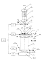
図1は、本実施例で使用される投影露光装置の概略を示す。図1において、レチクルRは光源1と、照明光整形光学系2〜リレーレンズ8よりなる照明光学系とにより長方形のスリット状の照明領域21により均一な照度で照明され、スリット状照明領域21内のレチクルRの回路パターン像が投影光学系13を介してウェハW上に転写される。光源1としては、F2エキシマレーザー、ArFエキシマレーザあるいはKrFエキシマレーザ等のエキシマレーザ光源、金属蒸気レーザ光源、又はYAGレーザの高調波発生装置等のパルス光源、又は水銀ランプと楕円反射鏡とを組み合わせた構成等の連続光源が使用できる。
【0046】
パルス光源の場合、露光のオン又はオフはパルス光源用の電源装置からの供給電力の制御により切り換えられ、連続光源の場合、露光のオン又はオフは照明光整形光学系2内のシャッタにより切り換えられる。但し、本実施例では後述のように可動ブラインド(可変視野絞り)7が設けられているため、可動ブラインド7の開閉によって露光のオン又はオフを切り換えてもよい。
【0047】
図1において、光源1からの照明光は、照明光整形光学系2により光束径が所定の大きさに設定されてフライアイレンズ3に達する。フライアイレンズ3の射出面には多数の2次光源が形成され、これら2次光源からの照明光は、コンデンサーレンズ4によって集光され、固定の視野絞り5を経て可動ブラインド(可変視野絞り)7に達する。図1では視野絞り5は可動ブラインド7よりもコンデンサーレンズ5側に配置されているが、その逆のリレーレンズ系8側へ配置しても構わない。
【0048】
視野絞り5には、長方形のスリット状の開口部が形成され、この視野絞り5を通過した光束は、長方形のスリット状の断面を有する光束となり、リレーレンズ系8に入射する。スリットの長手方向は紙面に対して垂直な方向である。リレーレンズ系8は可動ブラインド7とレチクルRのパターン形成面とを共役にするレンズ系であり、可動ブラインド7は後述の走査方向(X方向)の幅を規定する2枚の羽根(遮光板)7A、7B及び走査方向に垂直な非走査方向の幅を規定する2枚の羽根(不図示)より構成されている。走査方向の幅を規定する羽根7A及び7Bはそれぞれ駆動部6A及び6Bにより独立に走査方向に移動できるように支持され、不図示の非走査方向の幅を規定する2枚の羽もそれぞれ独立に駆動できるように支持されている。本実施例では、固定の視野絞り5により設定されるレチクルR上のスリット状の照明領域21内において、更に可動ブラインド7により設定される所望の露光領域内にのみ照明光が照射される。リレーレンズ系8は両側テレセントリックな光学系であり、レチクルR上のスリット状の照明領域21ではテレセントリック性が維持されている。
【0049】
レチクルRはレチクルステージRSTに保持されている。レチクルステージRSTは干渉計22で位置を検出しレチクルステージ駆動部10により駆動される。レチクルRの下部には光学素子G1が保持され、レチクルステージRST走査駆動時にはレチクルRと共に走査される。スリット状の照明領域21内で且つ可動ブラインド7により規定されたレチクルR上の回路パターンの像が、投影光学系13を介してウェハW上に投影露光される。
【0050】
投影光学系13の光軸に垂直な2次元平面内で、スリット状の照明領域21に対するレチクルRの走査方向を+X方向(又は−X方向)として、投影光学系13の光軸に平行な方向をZ方向とする。
【0051】
この場合、レチクルステージRSTはレチクルステージ駆動部10に駆動されてレチクルRを走査方向(+X方向又は−X方向)に走査し、可動ブラインド7の駆動部6A、6B、及び非走査方向用の駆動部の動作は可動ブラインド制御部11により制御される。レチクルステージ駆動部10及び可動ブラインド制御部11の動作を制御するのが、装置全体の動作を制御する主制御系12である。
【0052】
レチクルステージRSTに保持された光学素子G1と投影光学系13の間にはレチクル面位置検出系ROが構成されている。
【0053】
補正光学素子G1によるディストーションの補正方法については特開平11−045842号公報に開示されている方式と同様であるのでここでは説明を省略する。
【0054】
一方、ウェハWは不図示のウェハ搬送装置によりウェハステージWSTに保持され、ウェハステージWSTは、投影光学系13の光軸に垂直な面内でウェハWの位置決めを行うと共にウェハWを±X方向に走査するXYステージ、及びZ方向にウェハWの位置決めを行うZステージ等より構成されている。ウェハステージWSTの位置は干渉計23により検出される。ウェハW上方には、オフ・アクシス方式のアライメントセンサ16が構成されている。アライメントセンサ16により、ウェハ上のアライメントマークが検出され、制御部17により処理され、主制御系12に送られる。主制御系12は、ウェハステージ駆動部15を介してウェハステージWSTの位置決め動作及び走査動作を制御する。
【0055】
そして、レチクルR上のパターン像をスキャン露光方式で投影光学系13を介してウェハW上の各ショット領域に露光する際には、図1の視野絞り5により設定されるスリット状の照明領域21に対して−X方向(又は+X方向)に、レチクルRを速度VR で走査する。また、投影光学系13の投影倍率をβとして、レチクルRの走査と同期して、+X方向(又は−X方向)に、ウェハWを速度VW(=β・VR)で走査する。これにより、ウェハW上のショット領域にレチクルRの回路パターン像が逐次転写される。
【0056】
図2を用いてレチクル面位置検出系ROについて説明する。まずレチクル面位置検出系の基本的な検出原理を説明すると、被検面であるレチクルパターン面に光束を斜め方向から照射し、被検面で反射した光束の所定面上への入射位置を位置検出素子で検出し、その位置情報から被検面のZ方向(投影光学系13の光軸方向)の位置情報を検出している。本図では1系統についてのみ説明するが、走査方向とほぼ直交する方向に設定された複数の光束を被検面上の複数の計測点に投影し、各々の計測点で求めたZ方向の位置情報を用いて被検面の傾き情報を算出している。さらに、レチクルRが走査されることにより走査方向にも複数の計測点でのZ方向の位置情報が計測出来る。これらの位置情報より、レチクルRのパターン面の面形状が算出可能となる。
【0057】
次にレチクル面位置検出系の各要素について説明する。図2において、30はレチクル面位置検出系の光源部である。31はレチクル面位置検出用の発光光源である。32は駆動回路であり、発光光源31から発せられる光の強度を任意にコントロール可能なよう構成している。
【0058】
発光光源31から発せられた光は、コリメーターレンズ33、集光レンズ34、によって光ファイバーなどの光伝達手段35に導かれている。
【0059】
光伝達手段35から発せられた光束は照明レンズ36により、スリット37を照明する。スリット37上にはレチクルRのパターン面の面位置計測用マーク37Aが施されており、該マーク37Aは結像レンズ38により補正光学系G2、ミラー39を介して被検面であるレチクルRのパターン面上に投影されている。結像レンズ38によりスリット37とレチクルRのパターン面の表面は光学的な共役関係になっている。同図では説明し易くするために主光線のみを示している。レチクルRのパターン面に結像したマーク像に基づく光束はレチクルRのパターン面で反射し、ミラー40、補正光学系G3を介して結像レンズ41により最結像位置42上にマーク像を再結像する。再結像位置42に再結像したマーク像に基づく光束は拡大光学系43により集光されて位置検出用の受光素子44上に略結像している。受光素子44からの信号はレチクル面位置信号処理系45にて計測処理され、被検面であるレチクルRのパターン面のZ、及び傾きの情報として処理される。
【0060】
図2は、断面図を示しため、1系統しか図示していないが、実際には複数配置することも可能である。また、図2ではレチクル面位置検出系検出光のレチクルRパターン面への入射方向を、走査方向と平行な方向から示しているがこれに限定するものでは無く、走査方向と直交する方向あるいは任意の角度の方向から入射する構成でもかまわない。
【0061】
図4に補正光学系G2、G3を用いた収差補正原理について説明する。
第一の補正方法としては、非計測方向断面の収束光束中に補正光学素子G1とほぼ同様な厚み寸法、ほぼ同様な傾け角度、さらにほぼ同様な屈性率を持った平行平面板を挿入し非計測断面方向の光軸方向のピント位置を合わせる方法がある。第二の補正方法としては、結像系を構成するレンズを計測方向の断面と非計測方向の断面にパワーの異なる光学系を構成することにより計測断面の光軸方向の結像位置に非計測断面の結像位置を合わせこむ方法である。
【0062】
図4aに第一の補正方法を示す。図4aは図3bに対応する非計測方向の断面を示した図である。投光光学系に補正光学系G2、受光光学系に補正光学系G3を構成している。補正光学系G2、G3は図3aに示した補正光学素子G1と計測光との角度に対応した角度分傾けて配置されている。また、厚み寸法も補正光学素子G1とほぼ同様な寸法となっており、屈折率についても同様である。補正光学系G2、G3が非計測方向断面の収束光束中に傾けて配置されるので、非計測方向のピント位置が移動する。このときの移動量が計測方向に発生するピントの移動量とほぼ一致することで、アスを補正することが可能となる。補正光学系G2、G3は、補正光学素子G1とほぼ同じ厚さ寸法としたが、設計上あるいは配置上の制約がある場合には変更することが可能である。厚さ寸法を厚くする場合は、傾ける角度は少なくなる。逆に厚さ寸法が薄くなる場合には、傾け角度は大きくなる。厚さ寸歩と傾け角度の間系で、移動するピント量が補正すべき量とほぼ等しくなれば補正することが可能となる。
【0063】
さらに、図4aでは投光光学系、受光光学系の両方に補正光学系G2、G3を構成したが、どちらか一方にのみ配置してもかまわない。この場合、どちらか一方にのみ配置する補正光学系で発生するピント移動量が、必要補正量となれば良い。
【0064】
図4bに第二の補正方法を示す。図4aとの違いは補正光学系G2、G3が平行平板ではなく、シリンドリカルレンズを用いたことである。非計測方向にパワーを持つように補正光学素子(シリンドリカルレンズ)G2、G3を配置することで、非計測方向のピント位置が移動する。この移動量が図3aで示す計測方向のピント移動量に対応した量になるようにシリンドリカルレンズの曲率を決定する。このことでアスを補正することが可能となる。色収差の補正方法としては、クサビ形状の光学素子を配置することで補正が可能である。
【0065】
次に図5を用いて、補正光学素子G1について説明する。図5aは補正光学素子G1がレチクルRとともに走査される場合で、レチクルRが投影光学系13の光軸上に位置している状態を示している。レチクルRに示した斜線部がパターン部である。照明領域21の範囲で照明されたパターン領域の照明像は、投影光学系13を介し、ウェハに転写される。照明領域21で照明され投影光学系13に向う露光光を21a、21bで示す。また、レチクル面位置検出系ROの主光線をROa、RObで示す。
【0066】
図5bに、レチクルRが走査され端部に移動した状態を示す。図5bにおいて、補正光学素子G1は、ディストーション補正の目的ためには図中の実線で示す大きさがあれば良い。しかしながら、実線で示す大きさの場合レチクル面位置検出系ROの主光線RObは一部が補正光学素子G1を透過出来なくなってしまいレチクルRのパターン面位置が計測出来ない。補正光学素子G1が図中派線で示した大きさG1bであればレチクル面位置検出系ROの主光線RObが補正光学素子G1を透過することが出来るため、レチクルRのパターン面を計測することが可能な構成となる。反対側のG1aについては説明を省略するが、G1bと同様である。図5以外の図は補正光学素子G1を図示の関係上レチクルRよりも小さく示しているが、正確には図5に示した形状である。
【0067】
計測されたレチクルRのパターン面の面形状をもとに補正を行う方式については、従来例と同様であれば良いので、ここでは詳細な説明を省略する。主な補正手段としては、面形状に対応して、ウェハステージの走査位置すなわち高さ方向の位置あるいは傾きを補正する。あるいは、投影光学系内の光学素子を駆動し、像面形状をレチクルパターン面の面形状に対応した形状に補正する。あるいは、レチクル面形状そのものを補正する手段を構成し補正する等の補正を行うものである。
【0068】
以上のように実施例1によれば、レチクルステージRSTに補正光学素子G1が保持されることにより、補正光学素子G1をレチクルR近傍に構成することが可能となる。さらにレチクルRのパターン面の面位置を、補正光学素子G1を介して計測する構成とすることで、レチクル面位置検出系ROの配置構成が可能となる。また、レチクルRのパターン面の面位置を、補正光学素子G1を介して計測することで発生する収差を、補正光学系G2、G3により補正可能であるため、精度よく検出することが可能となる。
【0069】
【実施例2】
図6を用いて実施例2について説明する。実施例1との違いは、実施例1では補正光学素子G1がレチクルステージRSTに保持される構成で、レチクルRとともに走査される構成であったものが、実施例2においては走査されることは無く固定部に配置される構成としたものである。実施例1と同一なものは説明を省略する。
【0070】
補正光学系G2、G3は配置、補正原理等実施例1の場合と同様である。
【0071】
実施例2の形態の場合、補正光学素子G1はレチクルRとともに走査されないため、照明領域21の範囲で照明された露光光が透過する大きさであれば良いことになる。
【0072】
レチクルRとともに走査されないため、レチクルステージRSTにレチクルRを吸着した状態でのレチクルRの面形状に起因するディストーションは補正できないというデメリットが生じる。また、補正光学素子G1はレチクルステージRSTの可動部との干渉を避けた位置に配置するため、実施例1の補正光学素子G1よりもレチクルRから遠ざかった位置に配置されることになる。このため、ディストーション補正精度が低下するというデメリットも生じる。
【0073】
しかしながら、レチクルステージRSTの可動部に補正光学素子G1を搭載しないため、可動部の重量が軽く構成でき、制御特性が向上するというメリットがある。
【0074】
補正光学素子G1がレチクルRとともに走査されない構成であっても、レチクル面位置検出系ROが補正光学素子G1を介してレチクルRのパターン面を検出する構成とすることが可能である。
【0075】
実施例2の場合の補正光学素子G1について説明する。図5cはレチクルRが投影光学系13の光軸上に位置している状態を示している。照明領域21の範囲で照明されたパターン領域の照明像は、投影光学系13を介し、ウェハに転写される。照明領域21で照明され投影光学系13に向う露光光を21a、21bで示す。また、レチクル面位置検出系ROの主光線をROa、RObで示す。
【0076】
図5cの場合は、レチクルRが走査されても補正光学素子G1は走査されないため、補正光学素子G1は、ディストーション補正の目的ためには図中の実線で示す大きさがあれば良い。しかしながら、実線で示す大きさの場合レチクル面位置検出系ROの主光線RObは一部が補正光学素子G1を透過出来なくなってしまいレチクルRのパターン面位置が計測出来ない。補正光学素子G1が図中派線で示した大きさG1cであればレチクル面位置検出系ROの主光線RObが補正光学素子G1を透過することが出来るため、レチクルRのパターン面を計測することが可能な構成となる。
【0077】
このように実施例2においても、レチクルRのパターン面の面位置を、補正光学素子G1を介して計測する構成とすることで、レチクル面位置検出系ROの配置構成が可能となる。また、レチクルRのパターン面の面位置を、補正光学素子G1を介して計測することで発生する収差を、補正光学系G2、G3により補正可能であるため、精度よく検出することが可能となる。
【0078】
本発明によれば、露光時のマスク熱変形などによって生じたレチクルのたわみあるいは、レチクルが交換され吸着固定された場合に、レチクル間の面形状差により発生する変形量差が、斜入射方式のレチクル面位置検出系によって検出される。そして、この検出結果に基づいて補正量が演算され、補正される。レチクルパターン面の面形状により発生するディストーション等が補正されることにより、パターン像の湾曲などが抑制され、レチクルパタ−ンの正確で安定した像が得られるという利点がある。
【0079】
また、補正光学素子により、レチクルの自重たわみやレチクル吸着固定時に吸着部の面形状とレチクルの面形状の組み合わせによって発生するレチクルの変形に起因するディストーションおよび投影光学系の製造調整残差として発生するディストーションが補正光学素子により補正されることで、パターン像の湾曲などが抑制され、レチクルパタ−ンの正確で安定した像が得られるという利点がある。
【0080】
次に、図7及び図8を参照して、上述の走査型露光装置100を利用したデバイスの製造方法の実施例を説明する。図7は、デバイス(ICやLSIなどの半導体チップ、LCD、CCD等)の製造を説明するためのフローチャートである。ここでは、半導体チップの製造を例に説明する。ステップ1(回路設計)ではデバイスの回路設計を行う。ステップ2(マスク製作)では、設計した回路パターンを形成したマスクを製作する。ステップ3(ウェハ製造)ではシリコンなどの材料を用いてウェハを製造する。ステップ4(ウェハプロセス)は前工程と呼ばれ、マスクとウェハを用いてリソグラフィ技術によってウェハ上に実際の回路を形成する。ステップ5(組み立て)は後工程と呼ばれ、ステップ4によって作成されたウェハを用いて半導体チップ化する工程であり、アッセンブリ工程(ダイシング、ボンディング)、パッケージング工程(チップ封入)等の工程を含む。ステップ6(検査)では、ステップ5で作成された半導体デバイスの動作確認テスト、耐久性テストなどの検査を行う。こうした工程を経て半導体デバイスが完成し、これが出荷(ステップ7)される。
【0081】
図8は、ステップ4のウェハプロセスの詳細なフローチャートである。ステップ11(酸化)ではウェハの表面を酸化させる。ステップ12(CVD)では、ウェハの表面に絶縁膜を形成する。ステップ13(電極形成)では、ウェハ上に電極を蒸着などによって形成する。ステップ14(イオン打ち込み)ではウェハにイオンを打ち込む。ステップ15(レジスト処理)ではウェハに感光剤を塗布する。ステップ16(露光)では、露光装置1によってマスクの回路パターンをウェハに露光する。ステップ17(現像)では、露光したウェハを現像する。ステップ18(エッチング)では、現像したレジスト像以外の部分を削り取る。ステップ19(レジスト剥離)では、エッチングが済んで不要となったレジストを取り除く。これらのステップを繰り返し行うことによってウェハ上に多重に回路パターンが形成される。本実施例の製造方法によれば従来よりも高品位のデバイスを製造することができる。
【0082】
以上、本発明の好ましい実施例を説明したが、本発明はこれらに限定されずその要旨の範囲内で種々の変形及び変更が可能である。
【0083】
【発明の効果】
本発明によれば、高精度なマスクのたわみ検出を実現しつつ装置の大型化を防止してマスクパターンの投影を良好に行う露光装置を提供することができる。
【図面の簡単な説明】
【図1】 本発明の実施例1の露光装置の概略断面図である。
【図2】 レチクル面位置検出系を説明するための概略断面図である。
【図3】 計測方向の断面図(結像状態を示す図)及び非計測方向の断面図(結像状態を示す図)である。
【図4】 第1及び第2の補正原理の説明図である
【図5】 光軸上、端部及び補正光学素子固定配置における補正光学素子の説明図である。
【図6】 本発明の実施例2の露光装置の概略断面図である。
【図7】 本発明の半導体デバイス製造方法のフローチャートである。
【図8】 本発明の半導体デバイス製造方法のフローチャートである。
【符号の説明】
13 投影光学系
G1 補正光学素子
G2、G3 補正光学系
RO レチクル面位置検出系[0001]
[Industrial application fields]
The present invention relates to an exposure apparatus that exposes a pattern (such as a wafer or a glass plate) on a mask or reticle (in the present application, these terms are used interchangeably) in a manufacturing process of a semiconductor integrated circuit, a liquid crystal display element, and the like. About. The present invention is suitable, for example, for a scanning projection exposure apparatus.
[0002]
[Prior art]
Conventionally, when a semiconductor element, a liquid crystal display element, a thin film magnetic head, or the like is manufactured by a photolithography process, a photomask or reticle (hereinafter referred to as reticle) pattern is transferred onto a photosensitive substrate wafer or glass plate (hereinafter referred to as wafer). Projection exposure apparatuses have been proposed. In recent years, patterns of semiconductor elements and the like are increasingly miniaturized. In order to realize this, it is necessary to increase the resolving power of the projection optical system. In order to increase the resolving power, there are techniques such as shortening the wavelength of the exposure light or increasing the numerical aperture of the projection optical system.
[0003]
On the other hand, the chip pattern of one semiconductor element tends to increase in size. Therefore, there is a need for an apparatus that can expose a pattern with a larger area.
[0004]
In order to satisfy the above two items, a projection optical system having a large exposure area and high resolving power is required. However, the larger the exposure area and the higher the resolving power, the more difficult it is to maintain the imaging performance such as distortion in the entire exposure area with a predetermined accuracy.
[0005]
Therefore, what is currently attracting attention is a scanning exposure apparatus. In a scanning exposure apparatus, a reticle pattern is transferred to a wafer while scanning the reticle and wafer relatively synchronously with respect to a rectangular or arcuate slit-like illumination area.
[0006]
In this system, only a part of the projection optical system is used by illuminating the reticle in a slit shape. For this reason, there is an advantage that it is easy to maintain imaging performance such as distortion at a predetermined accuracy.
[0007]
In addition, by illuminating the reticle in a slit shape, the maximum diameter of the effective exposure area of the projection optical system can be used, and by scanning, the exposure area can be enlarged without being restricted by the optical system. There are advantages.
[0008]
However, further miniaturization of the pattern is currently required, and it is necessary to reduce the image distortion (distortion) of the pattern image even in the scanning exposure apparatus.
[0009]
Naturally, it is necessary to reduce various aberrations of the projection optical system in order to reduce distortion. Therefore, the projection optical system mounted on the conventional stepper is optically designed under such conditions that various aberrations and distortion are reduced on average in the entire projection visual field. Then, in order to keep the various aberrations and distortion within the allowable range at the time of design, the lens element and the optical member are processed with high accuracy, and the various aberrations are actually measured, for example, the air interval between the lenses, the inclination of the lens, and the like. It was assembled as a projection optical system by repeating complicated and time-consuming assembly, adjustment, and inspection such as adjusting parallel decentering.
[0010]
Of the various aberrations, particularly distortion, it is possible to adjust a symmetric component or a regular asymmetric component with respect to the optical axis by the above-described adjustment method.
[0011]
However, the so-called random component has a problem that it cannot be adjusted by the adjusting means described above.
[0012]
Therefore, in order to alleviate the difficulty in manufacturing such a high-precision projection optical system as much as possible, and to make sure that random components can be kept within the allowable range at the time of design. Measures the image distortion characteristics of the optical system and polishes so that the principal ray passing through each point in the projection field is partially deflected so that the measured image distortion characteristic is minimized at each point in the projection field. A method of inserting the optical correction plate (correction optical element) into the projection optical path is disclosed in, for example, Japanese Patent Application Laid-Open No. 8-203805. Japanese Patent Laid-Open No. 8-203805 is a correction method related to a stepper using an optical correction plate.
[0013]
JP-A-11-045842 discloses a correction method using an optical correction plate in a scanning exposure apparatus. In Japanese Patent Application Laid-Open No. 11-045842, when a pattern on a mask is scanned and exposed on a photosensitive substrate by a scanning projection exposure apparatus, static image distortion characteristics are averaged over the width in the projection area in the scanning direction. Focusing on dynamic image distortion characteristics, at least random components of the dynamic image distortion characteristics are obtained by locally polishing the surface of a transparent parallel plate (optical correction plate). Correction is performed by placing a correction plate in the projection optical path.
[0014]
Japanese Patent Laid-Open No. 11-031652 is disclosed as focusing on the production and measurement of an optical correction plate. Japanese Patent Application Laid-Open No. 11-031652 discloses a substrate in which a wedge angle is provided on the optical correction plate in order to prevent interference of the back light of the optical correction plate when measuring the surface shape of the optical correction plate using an interferometer. It is.
[0015]
Although the conventional example regarding distortion has been described, in order to cope with miniaturization, in addition to distortion, it is necessary to consider the variation amount of the imaging characteristics of the projected image by the projection optical system. With the miniaturization, the allowable range of the variation amount of the imaging characteristics is narrowed. Therefore, conventionally, in a projection exposure apparatus, Japanese Patent Application Laid-Open No. 60-78455 corrects a variation amount of imaging characteristics (for example, magnification, focal position, etc.) caused by the projection optical system absorbing illumination light. As disclosed in Japanese Patent Laid-Open No. 63-58349 or the like, the amount of light incident on the projection optical system is detected, and the amount of fluctuation in the imaging characteristics of the projection optical system is corrected according to the detected amount of light. An image characteristic correction mechanism was provided.
[0016]
For example, the mechanism disclosed in Japanese Patent Application Laid-Open No. 60-78455 will be briefly described. A model corresponding to the fluctuation characteristics of the imaging characteristics of the projection optical system is prepared in advance, and the wafer is placed on the wafer stage. The amount of light energy incident on the projection optical system at a predetermined time interval is obtained by a photoelectric sensor or the like, and an integrated value of the amount of light energy is applied to the model to calculate the amount of variation in imaging characteristics. In this case, the exposure time for obtaining the integrated value of the light energy incident on the projection optical system is calculated, for example, by constantly monitoring a signal indicating that the shutter for opening and closing the illumination light is in an open state. Therefore, the variation amount of the imaging characteristics of the projection optical system can be calculated according to the model, and correction is performed based on this variation amount. Thereby, the problem of fluctuations in image formation characteristics due to absorption of illumination light by the projection optical system has been solved.
[0017]
However, since the illumination light also passes through the mask, the mask is thermally deformed due to the absorption of the illumination light, and this also disadvantageously changes the imaging characteristics. In particular, since the mask has a pattern drawn by a light shielding film such as a chromium film, the heat absorption by the light shielding film is large unlike a glass substrate portion having high transmittance. Furthermore, in recent years, there is a tendency to adopt a technique for reducing the light-shielding film on the mask for the purpose of preventing flare in the optical system, but this further increases heat absorption in the light-shielding film.
[0018]
Further, the circuit pattern formed by the light shielding film of the mask is not necessarily distributed uniformly over the entire mask, but may be distributed unevenly. In this case, there is a possibility that the mask locally rises in temperature and generates anisotropic distortion. Similarly, anisotropic distortion may occur when only a part of the mask pattern is exposed using a variable field stop (reticle blind) or the like. Due to the mask distortion generated in this way, an anisotropic distortion also occurs in the projected image. In this case, it is not sufficient to correct only the magnification component.
[0019]
Further, it is difficult to uniformly correct the thermal deformation of the mask because the amount of thermal deformation and thus the amount of change in imaging characteristics differ depending on the type of mask used. That is, for example, the fluctuation amount of the imaging characteristic due to the thermal deformation of the mask used for adjusting the imaging characteristic at the time of shipment of the projection exposure apparatus can be recognized and corrected as the fluctuation characteristic of the imaging characteristic of the projection exposure apparatus. However, if other masks are used, the amount of thermal deformation is different, so accurate correction cannot be performed. In particular, when exposure is performed by successively exchanging masks, the amount of variation in imaging characteristics can accumulate and become a large error unless the amount of thermal deformation of each mask is taken into consideration.
[0020]
As a countermeasure against this, a projection exposure apparatus that corrects changes in optical characteristics caused by thermal deformation of the mask, including the heat absorption rate of chromium forming the mask pattern, the chromium presence rate in the pattern, and the like as parameters. No. 192317. The image forming characteristic correction method disclosed in Japanese Patent Laid-Open No. 4-192317 has been proposed on the premise of a batch exposure method (full field method).
In the scanning exposure method, since the mask is scanned with respect to the illumination area at the time of exposure, the factors to be considered regarding the mask (such as the cooling effect of the mask accompanying the mask scanning) have increased. There is an inconvenience that the calculation is complicated compared to the case of the batch exposure method.
[0021]
Japanese Patent Laid-Open No. 10-214780 discloses a projection exposure apparatus that corrects changes in optical characteristics caused by thermal deformation of a mask in a scan exposure system. Japanese Patent Application Laid-Open No. 10-214780 is a system in which a deflection generated in a mask is detected by an oblique incidence optical system, and a mask deflection amount is calculated and corrected.
[0022]
The mechanism in the scan exposure method disclosed in Japanese Patent Laid-Open No. 10-214780 will be briefly described. The exposure light beam in the scan exposure method has a narrow width in the scanning direction and a wide width in the orthogonal direction. Focusing on the irradiation range of the exposure light beam, the deflection in the scanning direction can be dealt with by controlling the focus or leveling, and only the deflection in the direction orthogonal to the scanning direction is corrected, which is practically good. Pattern projection can be performed. The correction is performed by driving the piezoelectric elements arranged at both ends of the mask and deforming the mask so as to correct the deflection of the mask. A plurality of piezoelectric elements are arranged in the direction in which the mask is scanned and moved.
[0023]
Further, the deflection detection is performed by detecting the deflection of the mask at a single point or by detecting the deflection at a plurality of points and calculating an optimal deflection correction amount by an average or least square method. As a technique for detecting deflection at a plurality of points, a plurality of mask deflection detection systems are provided, or a plurality of beams are obtained from light output from one light source using a diffraction grating. Furthermore, mask deflection detection points are set on both sides of the exposure light irradiation area in the mask scanning direction, and the amount of mask deflection is detected before the exposure light irradiation area in the mask scanning direction. It has also been proposed to correct the mask pattern projection image in real time in accordance with the amount of deflection of the mask in the illumination area.
[0024]
[Problems to be solved by the invention]
Japanese Laid-Open Patent Publication No. 11-045842 discloses a conventional example corresponding to distortion, in particular, a scanning exposure apparatus, which uses a correction optical element. Japanese Patent Laid-Open No. 10-214780 discloses a method of correcting and correcting the mask corresponding to the deflection and deformation of the mask.
[0025]
In the method disclosed in Japanese Patent Application Laid-Open No. 11-045842, the use of a correction optical element can cope with distortion caused by deformation occurring when the projection optical system or the mask is held, but due to thermal deformation of the mask due to exposure, etc. There is a problem that it cannot cope with the change in optical characteristics that occurs. Furthermore, when the mask is replaced, there is a problem that it is not possible to cope with the distortion generated due to the mask surface shape.
[0026]
The method disclosed in Japanese Patent Application Laid-Open No. 10-214780 measures and corrects the surface shape of the mask, so that it is possible to deal with factors caused by the mask, but it cannot cope with the distortion of the projection optical system. is there. For this reason, it is necessary to employ both methods disclosed in Japanese Patent Laid-Open Nos. 11-045842 and 10-214780 simultaneously.
[0027]
As disclosed in Japanese Patent Application Laid-Open No. 10-214780, an oblique incidence type deflection detecting means is configured on the mask back surface side (mask pattern surface side), and a correction optical element for distortion correction is a mask-projection optical system. In the case of the interposition, it is necessary to arrange the mask, the deflection detecting means, the correction optical element, and the projection optical system in this order.
[0028]
It is desirable to arrange the correction optical element as close to the mask as possible. Therefore, in order to arrange the correction optical element as close to the mask as possible and constitute the deflection detection means, it is necessary for the detection light of the deflection detection means to detect the mask pattern surface via the correction optical element.
[0029]
The correction optical element is a plate-like optical component having a constant thickness, and a part of the surface shape is slightly polished for correction. Therefore, the detection light emitted from the illumination optical system of the detection means is incident on the correction optical element from the oblique direction, reflected by the mask pattern surface, and incident on the correction optical element from the oblique direction again. Then, it is guided to the detection unit. At this time, aberration occurs. The generation principle will be described with reference to FIG. FIG. 3a shows a cross section in the measurement direction of the reticle surface position detection system. The pattern image for measurement illuminated by an illumination optical system (not shown) is projected onto the pattern surface of the reticle R via the projection optical system and the correction optical element G1, and the reflected pattern image is again received by the correction optical element G1 and the light reception. The image is formed on the
[0030]
FIG. 3b shows a cross section in the non-measurement direction. As shown in FIG. 3b, when attention is paid to the cross section in the non-measurement direction, the correction optical element G1 is arranged perpendicular to the optical axis in the light paths of the light projecting optical system and the light receiving optical system.
[0031]
From this, the refraction angle of the light beam having the aperture angle is greatly different between the measurement cross section and the non-measurement cross section, and the image formation point in the measurement cross section direction and the image formation point in the non-measurement direction are in the optical axis direction at the image formation position. A so-called astigmatism (hereinafter referred to as “asp”) occurs. In particular, in the case of a detection optical system in which a light projecting optical system and a light receiving optical system are connected, the astigmatism on the light receiving re-imaging plane is doubled.
[0032]
A system in which a slit-shaped mark is used as a measurement mark, the slit-shaped mark is projected onto the pattern surface of the reticle R, and the position of the surface is detected by detecting the positional deviation of the mark by the
[0033]
Further, the correction optical element of the conventional example is configured to have a size that secures a region through which the illumination light that has exposed the mask is transmitted. For this reason, when the detection unit of the oblique incidence method detects the mask pattern surface via the correction optical element, there is a problem that the area where the mask pattern surface can be detected via the correction optical element is reduced by the oblique incidence angle. .
[0034]
In FIG. 3, the asphalt has been described. However, there is a problem in that chromatic aberration occurs due to the correction optical element G <b> 1 that is a parallel plate being tilted and inserted into the convergent light beam, and the detection accuracy is lowered.
[0035]
Corresponding to the wavelength width of the light used as the detection light, dispersion occurs due to the difference in refractive index for each wavelength, resulting in chromatic aberration.
[0036]
Accordingly, an object of the present invention is to provide an exposure apparatus that can accurately detect a deflection of a mask while preventing an increase in the size of the apparatus and projecting a mask pattern satisfactorily.
[0037]
In order to achieve the above object, an exposure apparatus according to one aspect of the present invention is disposed between a projection optical system having predetermined imaging characteristics, a mask on which a pattern to be transferred is formed, and the projection optical system. A correction optical element for reducing the distortion of the pattern, and a grazing incidence detection means that is disposed on the pattern surface side of the mask and detects the surface shape of the mask via the correction optical element. The detection means includes a correction optical system that corrects an optical aberration generated by detection through the correction optical element. .
[0038]
The detection unit may include a correction optical system that corrects an optical aberration (for example, astigmatism and / or chromatic aberration) generated by detection through the optical element.
[0039]
The detection means includes a light irradiation means having an illumination optical system that irradiates light to the mask from the oblique direction through the correction optical element and the correction optical system, and light irradiated by the light irradiation means is the mask. A light receiving means having an imaging optical system that receives the reflected light via the optical element and the correction optical system, and outputs a detection signal corresponding to the position of the reflected light received by the light receiving means. You may have a light detection means.
[0041]
A device manufacturing method as still another aspect of the present invention includes a step of projecting and exposing an object to be exposed using the above-described exposure apparatus, and a step of performing a predetermined process on the object to be exposed by projection. The claim of the device manufacturing method having the same operation as that of the above-described exposure apparatus extends to the device itself as an intermediate and final product. Such devices include semiconductor chips such as LSI and VLSI, CCDs, LCDs, magnetic sensors, thin film magnetic heads, and the like.
[0042]
Other objects and further features of the present invention will become apparent from the preferred embodiments described below with reference to the accompanying drawings.
[0043]
DETAILED DESCRIPTION OF THE INVENTION
Hereinafter, embodiments of the invention will be described in detail with reference to examples. In the first embodiment, a scanning type exposure apparatus to which the present invention is applied will be described. However, the present invention is not limited to the scanning type, and the same effect can be obtained even with a batch exposure type exposure apparatus.
[0044]
[Example 1]
A first embodiment of the present invention will be described with reference to FIG.
[0045]
FIG. 1 schematically shows a projection exposure apparatus used in this embodiment. In FIG. 1, a reticle R is illuminated with a uniform illuminance by a rectangular slit-shaped
[0046]
In the case of a pulsed light source, the on / off of exposure is switched by controlling the power supplied from the power supply device for the pulsed light source. In the case of a continuous light source, the on / off of exposure is switched by a shutter in the illumination light shaping
[0047]
In FIG. 1, the illumination light from the
[0048]
A rectangular slit-shaped opening is formed in the
[0049]
Reticle R is held on reticle stage RST. The position of reticle stage RST is detected by
[0050]
In a two-dimensional plane perpendicular to the optical axis of the projection
[0051]
In this case, the reticle stage RST is driven by the reticle
[0052]
Between the optical element G1 held on the reticle stage RST and the projection
[0053]
Since the distortion correction method by the correction optical element G1 is the same as the method disclosed in Japanese Patent Laid-Open No. 11-045842, the description thereof is omitted here.
[0054]
On the other hand, wafer W is held on wafer stage WST by a wafer transfer device (not shown), and wafer stage WST positions wafer W in a plane perpendicular to the optical axis of projection
[0055]
When the pattern image on the reticle R is exposed to each shot area on the wafer W via the projection
[0056]
The reticle surface position detection system RO will be described with reference to FIG. First, the basic detection principle of the reticle surface position detection system will be described. The reticle pattern surface, which is the test surface, is irradiated with a light beam from an oblique direction, and the incident position of the light beam reflected by the test surface on the predetermined surface is positioned. Detection is performed by a detection element, and position information in the Z direction (the optical axis direction of the projection optical system 13) of the surface to be detected is detected from the position information. In this figure, only one system will be described, but a plurality of light beams set in a direction substantially orthogonal to the scanning direction are projected onto a plurality of measurement points on the surface to be measured, and the positions in the Z direction obtained at the respective measurement points The tilt information of the test surface is calculated using the information. Further, by scanning the reticle R, position information in the Z direction at a plurality of measurement points can also be measured in the scanning direction. From these position information, the surface shape of the pattern surface of the reticle R can be calculated.
[0057]
Next, each element of the reticle surface position detection system will be described. In FIG. 2, reference numeral 30 denotes a light source unit of a reticle surface position detection system. Reference numeral 31 denotes a light source for detecting the reticle surface position. Reference numeral 32 denotes a drive circuit, which is configured so that the intensity of light emitted from the light emitting light source 31 can be arbitrarily controlled.
[0058]
The light emitted from the light emitting light source 31 is guided to a light transmission means 35 such as an optical fiber by a
[0059]
The light beam emitted from the light transmission means 35 illuminates the
[0060]
FIG. 2 shows only a single system to show a cross-sectional view, but in reality, a plurality of systems can be arranged. Further, in FIG. 2, the incident direction of the reticle surface position detection system detection light to the reticle R pattern surface is shown from a direction parallel to the scanning direction, but the present invention is not limited to this, and the direction orthogonal to the scanning direction or arbitrary It is also possible to adopt a configuration in which the light enters from the direction of the angle.
[0061]
FIG. 4 illustrates the principle of aberration correction using the correction optical systems G2 and G3.
As a first correction method, a parallel plane plate having substantially the same thickness dimension, substantially the same tilt angle as that of the correction optical element G1, and almost the same refractive index is inserted into the convergent light beam in the cross section in the non-measurement direction. There is a method of adjusting the focus position in the optical axis direction in the non-measurement cross-sectional direction. As a second correction method, the lens constituting the imaging system is not measured at the imaging position in the optical axis direction of the measurement cross section by configuring an optical system with different powers in the cross section in the measurement direction and the cross section in the non-measurement direction. This is a method of matching the imaging position of the cross section.
[0062]
FIG. 4a shows the first correction method. 4a is a diagram showing a cross section in the non-measurement direction corresponding to FIG. 3b. The light projecting optical system includes a correction optical system G2, and the light receiving optical system includes a correction optical system G3. The correction optical systems G2 and G3 are arranged so as to be inclined by an angle corresponding to the angle between the correction optical element G1 shown in FIG. Further, the thickness dimension is almost the same as that of the correction optical element G1, and the refractive index is also the same. Since the correction optical systems G2 and G3 are tilted and arranged in the convergent light beam in the non-measurement direction section, the focus position in the non-measurement direction moves. Since the movement amount at this time substantially coincides with the movement amount of the focus generated in the measurement direction, it is possible to correct asphalt. The correction optical systems G2 and G3 have substantially the same thickness as that of the correction optical element G1, but can be changed if there are restrictions on design or arrangement. When the thickness dimension is increased, the tilt angle is reduced. Conversely, when the thickness dimension is reduced, the tilt angle is increased. Correction can be made if the amount of focus to move is substantially equal to the amount to be corrected in the system between the thickness step and the tilt angle.
[0063]
Further, in FIG. 4a, the correction optical systems G2 and G3 are configured in both the light projecting optical system and the light receiving optical system, but they may be arranged in only one of them. In this case, the amount of focus movement that occurs in the correction optical system arranged only in one of them may be the required correction amount.
[0064]
FIG. 4b shows a second correction method. The difference from FIG. 4a is that the correction optical systems G2 and G3 use cylindrical lenses instead of parallel plates. By arranging the correction optical elements (cylindrical lenses) G2 and G3 so as to have power in the non-measurement direction, the focus position in the non-measurement direction moves. The curvature of the cylindrical lens is determined so that this movement amount corresponds to the focus movement amount in the measurement direction shown in FIG. This makes it possible to correct asphalt. As a method for correcting chromatic aberration, correction can be performed by arranging a wedge-shaped optical element.
[0065]
Next, the correction optical element G1 will be described with reference to FIG. FIG. 5 a shows a state where the correction
[0066]
FIG. 5b shows a state where the reticle R is scanned and moved to the end. In FIG. 5b, the correction optical element G1 only needs to have a size indicated by a solid line in the drawing for the purpose of distortion correction. However, in the case of the size indicated by the solid line, a part of the principal ray ROb of the reticle surface position detection system RO cannot pass through the correction optical element G1, and the pattern surface position of the reticle R cannot be measured. If the correction optical element G1 has the size G1b indicated by the drawing line in the figure, the principal ray ROb of the reticle surface position detection system RO can pass through the correction optical element G1, and therefore the pattern surface of the reticle R is measured. Is possible. The description of the opposite side G1a is omitted, but is the same as G1b. Although the drawings other than FIG. 5 show the correction optical element G1 smaller than the reticle R in the illustrated relationship, the shape is exactly the shape shown in FIG.
[0067]
Since the method for performing correction based on the measured surface shape of the pattern surface of the reticle R may be the same as that of the conventional example, detailed description thereof is omitted here. As a main correction means, the scanning position of the wafer stage, that is, the height direction position or inclination is corrected in accordance with the surface shape. Alternatively, the optical element in the projection optical system is driven to correct the image surface shape to a shape corresponding to the surface shape of the reticle pattern surface. Alternatively, correction such as correction is performed by configuring a means for correcting the reticle surface shape itself.
[0068]
As described above, according to the first embodiment, the correction optical element G1 is held near the reticle R by holding the correction optical element G1 on the reticle stage RST. Furthermore, by arranging the surface position of the pattern surface of the reticle R via the correction optical element G1, the arrangement configuration of the reticle surface position detection system RO becomes possible. In addition, since the aberration generated by measuring the surface position of the pattern surface of the reticle R through the correction optical element G1 can be corrected by the correction optical systems G2 and G3, it can be detected with high accuracy. .
[0069]
[Example 2]
Example 2 will be described with reference to FIG. The difference from the first embodiment is that the correction optical element G1 is held by the reticle stage RST in the first embodiment and is scanned together with the reticle R, but in the second embodiment, the scanning is performed. The configuration is such that it is arranged in the fixed part without any problem. A description of the same components as those in the first embodiment will be omitted.
[0070]
The correction optical systems G2 and G3 are the same as those in the first embodiment, such as arrangement and correction principle.
[0071]
In the case of the second embodiment, since the correction optical element G1 is not scanned together with the reticle R, it is sufficient that the exposure light illuminated in the range of the
[0072]
Since scanning is not performed with the reticle R, there is a demerit that the distortion caused by the surface shape of the reticle R in a state where the reticle R is attracted to the reticle stage RST cannot be corrected. Further, since the correction optical element G1 is disposed at a position avoiding interference with the movable part of the reticle stage RST, the correction optical element G1 is disposed at a position farther from the reticle R than the correction optical element G1 of the first embodiment. For this reason, there also arises a demerit that the distortion correction accuracy is lowered.
[0073]
However, since the correction optical element G1 is not mounted on the movable part of the reticle stage RST, there is an advantage that the weight of the movable part can be reduced and the control characteristics are improved.
[0074]
Even if the correction optical element G1 is not scanned with the reticle R, the reticle surface position detection system RO can be configured to detect the pattern surface of the reticle R via the correction optical element G1.
[0075]
The correction optical element G1 in the case of Example 2 will be described. FIG. 5 c shows a state where the reticle R is located on the optical axis of the projection
[0076]
In the case of FIG. 5c, since the correction optical element G1 is not scanned even when the reticle R is scanned, the correction optical element G1 only needs to have a size indicated by a solid line in the drawing for the purpose of distortion correction. However, in the case of the size indicated by the solid line, a part of the principal ray ROb of the reticle surface position detection system RO cannot pass through the correction optical element G1, and the pattern surface position of the reticle R cannot be measured. If the correction optical element G1 has the size G1c indicated by the line in the figure, the principal ray ROb of the reticle surface position detection system RO can pass through the correction optical element G1, so that the pattern surface of the reticle R is measured. Is possible.
[0077]
As described above, also in the second embodiment, the configuration of the reticle surface position detection system RO can be configured by measuring the surface position of the pattern surface of the reticle R through the correction optical element G1. In addition, since the aberration generated by measuring the surface position of the pattern surface of the reticle R through the correction optical element G1 can be corrected by the correction optical systems G2 and G3, it can be detected with high accuracy. .
[0078]
According to the present invention, the deflection of the reticle caused by mask thermal deformation at the time of exposure, or the deformation amount difference caused by the surface shape difference between the reticles when the reticle is replaced and fixed by suction is the oblique incidence method. It is detected by a reticle surface position detection system. Based on the detection result, the correction amount is calculated and corrected. By correcting distortion and the like generated by the surface shape of the reticle pattern surface, there is an advantage in that the curvature of the pattern image is suppressed and an accurate and stable image of the reticle pattern can be obtained.
[0079]
In addition, the correction optical element generates distortion due to reticle deformation caused by the combination of the surface shape of the suction portion and the surface shape of the reticle during reticle self-weight deflection and reticle suction and fixation, and production adjustment residuals of the projection optical system. Since the distortion is corrected by the correction optical element, there is an advantage that the curvature of the pattern image is suppressed and an accurate and stable image of the reticle pattern can be obtained.
[0080]
Next, an embodiment of a device manufacturing method using the above-described scanning exposure apparatus 100 will be described with reference to FIGS. FIG. 7 is a flowchart for explaining how to fabricate devices (ie, semiconductor chips such as IC and LSI, LCDs, CCDs, and the like). Here, the manufacture of a semiconductor chip will be described as an example. In step 1 (circuit design), the device circuit is designed. In step 2 (mask production), a mask on which the designed circuit pattern is formed is produced. In step 3 (wafer manufacture), a wafer is manufactured using a material such as silicon. Step 4 (wafer process) is called a pre-process, and an actual circuit is formed on the wafer by lithography using the mask and wafer. Step 5 (assembly) is called a post-process, and is a process for forming a semiconductor chip using the wafer created in
[0081]
FIG. 8 is a detailed flowchart of the wafer process in
[0082]
The preferred embodiments of the present invention have been described above, but the present invention is not limited to these embodiments, and various modifications and changes can be made within the scope of the gist thereof.
[0083]
【The invention's effect】
ADVANTAGE OF THE INVENTION According to this invention, the exposure apparatus which prevents the enlargement of an apparatus and implement | achieves a mask pattern favorably can be provided, implement | achieving the deflection | deviation of a highly accurate mask.
[Brief description of the drawings]
FIG. 1 is a schematic sectional view of an exposure apparatus according to
FIG. 2 is a schematic sectional view for explaining a reticle surface position detection system.
FIG. 3 is a cross-sectional view in a measurement direction (a diagram showing an imaging state) and a cross-sectional view in a non-measurement direction (a diagram showing an imaging state).
FIG. 4 is an explanatory diagram of first and second correction principles;
FIG. 5 is an explanatory diagram of the correction optical element on the optical axis, at the end, and in the fixed arrangement of the correction optical element.
FIG. 6 is a schematic sectional view of an exposure apparatus according to a second embodiment of the present invention.
FIG. 7 is a flowchart of a semiconductor device manufacturing method according to the present invention.
FIG. 8 is a flowchart of a semiconductor device manufacturing method according to the present invention.
[Explanation of symbols]
13 Projection optical system
G1 correction optical element
G2, G3 correction optical system
RO reticle surface position detection system
Claims (4)
転写されるべきパターンが形成されたマスクと前記投影光学系の間に配置され、前記パターンの歪みを低減するための補正光学素子と、
前記マスクのパターン面側に配置され、前記補正光学素子を介して前記マスクの面形状を検出する斜入射方式の検出手段とを有し、
前記検出手段は、前記補正光学素子を介して検出することで発生する光学収差を補正する補正光学系を有することを特徴とする露光装置。A projection optical system having predetermined imaging characteristics;
A correction optical element disposed between a mask on which a pattern to be transferred is formed and the projection optical system, and for reducing distortion of the pattern;
A grazing incidence detection means that is arranged on the pattern surface side of the mask and detects the surface shape of the mask via the correction optical element ;
An exposure apparatus comprising : a correction optical system that corrects an optical aberration generated by detecting the detection means via the correction optical element .
前記マスクに斜め方向から前記補正光学素子を介して光を照射する照明光学系と前記補正光学系とを有する光照射手段と、
前記光照射手段によって照射された光が前記マスクで反射し、その反射光を前記光学素子を介して受光する結像光学系と前記補正光学系とを有する受光手段と、
前記受光手段により受光した反射光の位置に対応した検出信号を出力する光検出手段とを有することを特徴とする請求項1記載の露光装置。The detection means includes
A light irradiation means having an illumination optical system for irradiating light from the oblique direction to the mask via the correction optical element and the correction optical system;
A light receiving means having an imaging optical system that reflects the light irradiated by the light irradiation means by the mask and receives the reflected light through the optical element; and the correction optical system;
Exposure apparatus according to claim 1, characterized in that it has a light detecting means for outputting a detection signal corresponding to the position of the reflected light received by said light receiving means.
前記投影露光された被露光体に所定のプロセスを行う工程とを有することを特徴とするデバイスの製造方法。A step of projecting and exposing an object to be exposed using the exposure apparatus according to claim 1 ;
And a step of performing a predetermined process on the projection-exposed object to be exposed.
Priority Applications (5)
| Application Number | Priority Date | Filing Date | Title |
|---|---|---|---|
| JP2002100581A JP3762323B2 (en) | 2002-04-02 | 2002-04-02 | Exposure equipment |
| TW092106979A TW583515B (en) | 2002-04-02 | 2003-03-27 | Exposure apparatus |
| US10/402,978 US6738128B2 (en) | 2002-04-02 | 2003-04-01 | Exposure apparatus |
| KR1020030020691A KR100566254B1 (en) | 2002-04-02 | 2003-04-02 | Exposure apparatus |
| CNB031086497A CN1244022C (en) | 2002-04-02 | 2003-04-02 | Exposure device |
Applications Claiming Priority (1)
| Application Number | Priority Date | Filing Date | Title |
|---|---|---|---|
| JP2002100581A JP3762323B2 (en) | 2002-04-02 | 2002-04-02 | Exposure equipment |
Publications (2)
| Publication Number | Publication Date |
|---|---|
| JP2003297726A JP2003297726A (en) | 2003-10-17 |
| JP3762323B2 true JP3762323B2 (en) | 2006-04-05 |
Family
ID=28449880
Family Applications (1)
| Application Number | Title | Priority Date | Filing Date |
|---|---|---|---|
| JP2002100581A Expired - Fee Related JP3762323B2 (en) | 2002-04-02 | 2002-04-02 | Exposure equipment |
Country Status (5)
| Country | Link |
|---|---|
| US (1) | US6738128B2 (en) |
| JP (1) | JP3762323B2 (en) |
| KR (1) | KR100566254B1 (en) |
| CN (1) | CN1244022C (en) |
| TW (1) | TW583515B (en) |
Families Citing this family (13)
| Publication number | Priority date | Publication date | Assignee | Title |
|---|---|---|---|---|
| JP4125177B2 (en) * | 2003-05-16 | 2008-07-30 | キヤノン株式会社 | Exposure equipment |
| JP2005085991A (en) * | 2003-09-09 | 2005-03-31 | Canon Inc | Exposure apparatus and manufacturing method of device using the apparatus |
| US7277231B2 (en) | 2004-04-02 | 2007-10-02 | Carl Zeiss Smt Ag | Projection objective of a microlithographic exposure apparatus |
| US7221434B2 (en) * | 2005-03-01 | 2007-05-22 | Canon Kabushiki Kaisha | Exposure method and apparatus |
| US7548302B2 (en) * | 2005-03-29 | 2009-06-16 | Asml Netherlands B.V. | Lithographic apparatus and device manufacturing method |
| US7317506B2 (en) * | 2005-03-29 | 2008-01-08 | Asml Netherlands B.V. | Variable illumination source |
| JP4724470B2 (en) | 2005-06-02 | 2011-07-13 | キヤノン株式会社 | Exposure method |
| JP2008192854A (en) * | 2007-02-05 | 2008-08-21 | Canon Inc | Immersion exposure apparatus |
| JP6039579B2 (en) * | 2011-12-13 | 2016-12-07 | キヤノン株式会社 | Nozzle tip manufacturing method |
| JP2013238670A (en) * | 2012-05-11 | 2013-11-28 | Canon Inc | Exposure apparatus, exposure method, method for manufacturing device, and aperture plate |
| CN105652598B (en) * | 2014-11-11 | 2018-03-02 | 上海微电子装备(集团)股份有限公司 | A kind of device and method for measuring mask aligner mask platform gradient and vertical degree |
| KR102395198B1 (en) | 2015-09-22 | 2022-05-06 | 삼성전자주식회사 | Method for correcting pattern and method for manufacturing using the same |
| JP6980443B2 (en) * | 2017-07-28 | 2021-12-15 | キヤノン株式会社 | Exposure equipment and article manufacturing method |
Family Cites Families (11)
| Publication number | Priority date | Publication date | Assignee | Title |
|---|---|---|---|---|
| US4624551A (en) | 1983-09-17 | 1986-11-25 | Nippon Kogaku K.K. | Light irradiation control method for projection exposure apparatus |
| JPS6078455A (en) | 1983-10-05 | 1985-05-04 | Nippon Kogaku Kk <Nikon> | Exposing device |
| IT8422427V0 (en) * | 1984-06-28 | 1984-06-28 | Carnielli & C Teodoro Spa | IMPROVED DEVICE FOR THE DETECTION OF DEVELOPED POWER, APPLICABLE ON CHAMBER BICYCLES. |
| JPH0821531B2 (en) | 1986-08-29 | 1996-03-04 | 株式会社ニコン | Projection optical device |
| JP3047461B2 (en) | 1990-11-26 | 2000-05-29 | 株式会社ニコン | Projection exposure apparatus, projection exposure method, and semiconductor integrated circuit manufacturing method |
| JP3893626B2 (en) | 1995-01-25 | 2007-03-14 | 株式会社ニコン | Projection optical apparatus adjustment method, projection optical apparatus, exposure apparatus, and exposure method |
| JPH09180989A (en) * | 1995-12-26 | 1997-07-11 | Toshiba Corp | Exposure system and method |
| JPH10214780A (en) | 1997-01-28 | 1998-08-11 | Nikon Corp | Projection aligner |
| US6549271B2 (en) | 1997-01-28 | 2003-04-15 | Nikon Corporation | Exposure apparatus and method |
| JP3715751B2 (en) | 1997-07-11 | 2005-11-16 | キヤノン株式会社 | Residual aberration correction plate and projection exposure apparatus using the same |
| JPH1145842A (en) | 1997-07-24 | 1999-02-16 | Nikon Corp | Projection aligner and exposure method, adjusting method of the aligner, and manufacture of circuit device |
-
2002
- 2002-04-02 JP JP2002100581A patent/JP3762323B2/en not_active Expired - Fee Related
-
2003
- 2003-03-27 TW TW092106979A patent/TW583515B/en not_active IP Right Cessation
- 2003-04-01 US US10/402,978 patent/US6738128B2/en not_active Expired - Fee Related
- 2003-04-02 CN CNB031086497A patent/CN1244022C/en not_active Expired - Fee Related
- 2003-04-02 KR KR1020030020691A patent/KR100566254B1/en not_active IP Right Cessation
Also Published As
| Publication number | Publication date |
|---|---|
| US20030184719A1 (en) | 2003-10-02 |
| JP2003297726A (en) | 2003-10-17 |
| CN1244022C (en) | 2006-03-01 |
| TW200305790A (en) | 2003-11-01 |
| TW583515B (en) | 2004-04-11 |
| KR100566254B1 (en) | 2006-03-29 |
| CN1448797A (en) | 2003-10-15 |
| KR20030079751A (en) | 2003-10-10 |
| US6738128B2 (en) | 2004-05-18 |
Similar Documents
| Publication | Publication Date | Title |
|---|---|---|
| EP1347501A1 (en) | Wavefront aberration measuring instrument, wavefront aberration measuring method, exposure apparatus, and method for manufacturing microdevice | |
| US7498596B2 (en) | Exposure method that obtains, prior to exposure, reticle surface form data and measurement position error, for scanning control | |
| JP2005175034A (en) | Aligner | |
| US7385672B2 (en) | Exposure apparatus and method | |
| KR20060120629A (en) | Exposure method and apparatus, and device manufacturing method | |
| JP2005175400A (en) | Aligner | |
| US7626680B2 (en) | Exposure apparatus and device fabrication method using the same | |
| JP3762323B2 (en) | Exposure equipment | |
| JP2006245157A (en) | Exposure method and device | |
| JP2010267966A (en) | Optical apparatus, exposure method and apparatus, and device manufacturing method | |
| JP4692862B2 (en) | Inspection apparatus, exposure apparatus provided with the inspection apparatus, and method for manufacturing microdevice | |
| US8854605B2 (en) | Illumination optical system, exposure apparatus, and device fabrication method | |
| JP3743576B2 (en) | Projection exposure apparatus and method for manufacturing semiconductor element or liquid crystal display element using the same | |
| WO2002042728A1 (en) | Method and apparatus for measuring aberration of projection optical system, and method and apparatus for exposure | |
| JP2001250760A (en) | Aberration measuring method, mask detecting method to use said method and exposure method | |
| US20050128447A1 (en) | Measuring method and apparatus, exposure method and apparatus using the same, and device manufacturing method | |
| US7148956B2 (en) | Exposure method | |
| JP2002195913A (en) | Apparatus and method for measuring aberration, exposure apparatus and method for producing device | |
| JP2005093697A (en) | Face position detecting device and method therefor, aligner and aberration correcting method | |
| JP3313932B2 (en) | Projection exposure equipment | |
| JP5089137B2 (en) | Exposure apparatus and device manufacturing method | |
| JP2006080444A (en) | Measurement apparatus, test reticle, aligner, and device manufacturing method | |
| JP2006287103A (en) | Exposure device, method, and device manufacturing method | |
| JP2000082654A (en) | Face position-detecting device and manufacture of device using the same | |
| JP2006108465A (en) | Optical characteristic measurement equipment and exposure device |
Legal Events
| Date | Code | Title | Description |
|---|---|---|---|
| A621 | Written request for application examination |
Free format text: JAPANESE INTERMEDIATE CODE: A621 Effective date: 20031210 |
|
| A977 | Report on retrieval |
Free format text: JAPANESE INTERMEDIATE CODE: A971007 Effective date: 20050824 |
|
| A131 | Notification of reasons for refusal |
Free format text: JAPANESE INTERMEDIATE CODE: A131 Effective date: 20050830 |
|
| A521 | Written amendment |
Free format text: JAPANESE INTERMEDIATE CODE: A523 Effective date: 20051026 |
|
| TRDD | Decision of grant or rejection written | ||
| A01 | Written decision to grant a patent or to grant a registration (utility model) |
Free format text: JAPANESE INTERMEDIATE CODE: A01 Effective date: 20060110 |
|
| A61 | First payment of annual fees (during grant procedure) |
Free format text: JAPANESE INTERMEDIATE CODE: A61 Effective date: 20060112 |
|
| R150 | Certificate of patent or registration of utility model |
Free format text: JAPANESE INTERMEDIATE CODE: R150 Ref document number: 3762323 Country of ref document: JP Free format text: JAPANESE INTERMEDIATE CODE: R150 |
|
| FPAY | Renewal fee payment (event date is renewal date of database) |
Free format text: PAYMENT UNTIL: 20090120 Year of fee payment: 3 |
|
| FPAY | Renewal fee payment (event date is renewal date of database) |
Free format text: PAYMENT UNTIL: 20100120 Year of fee payment: 4 |
|
| FPAY | Renewal fee payment (event date is renewal date of database) |
Free format text: PAYMENT UNTIL: 20110120 Year of fee payment: 5 |
|
| FPAY | Renewal fee payment (event date is renewal date of database) |
Free format text: PAYMENT UNTIL: 20120120 Year of fee payment: 6 |
|
| FPAY | Renewal fee payment (event date is renewal date of database) |
Free format text: PAYMENT UNTIL: 20130120 Year of fee payment: 7 |
|
| FPAY | Renewal fee payment (event date is renewal date of database) |
Free format text: PAYMENT UNTIL: 20140120 Year of fee payment: 8 |
|
| LAPS | Cancellation because of no payment of annual fees |