JP3750911B2 - Current control circuit - Google Patents
Current control circuit Download PDFInfo
- Publication number
- JP3750911B2 JP3750911B2 JP37476299A JP37476299A JP3750911B2 JP 3750911 B2 JP3750911 B2 JP 3750911B2 JP 37476299 A JP37476299 A JP 37476299A JP 37476299 A JP37476299 A JP 37476299A JP 3750911 B2 JP3750911 B2 JP 3750911B2
- Authority
- JP
- Japan
- Prior art keywords
- operational amplifier
- current
- voltage
- input terminal
- resistor
- Prior art date
- Legal status (The legal status is an assumption and is not a legal conclusion. Google has not performed a legal analysis and makes no representation as to the accuracy of the status listed.)
- Expired - Fee Related
Links
Images

Description
【0001】
【発明の属する技術分野】
本発明は、電流制御回路に関し、特に接触燃焼式ガスセンサ回路に有用な電流制御回路に関する。
【0002】
【従来の技術】
出願人は、接触燃焼式ガスセンサ回路に有用な電流制御回路に関する特許出願として、すでに特開平9−318584号を提案している。特開平9−318584号には、オペアンプを負帰還制御で用いる接触燃焼式ガスセンサ定電流駆動回路において、直流電源プラス端子からの定電圧を前記オペアンプの非反転入力端子に加えるようにすることにより、たとえ直流電源電圧変動があっても誤動作の起こらない信頼性の高い接触燃焼式ガスセンサ定電流駆動回路が開示されている。
【0003】
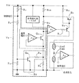
図3は、従来の接触燃焼式ガスセンサ回路に用いられる電流制御回路の一例を示す回路図である。図3において、センサ電流制御回路は、オペアンプ(演算増幅器)A1を備えたハイサイド定電流駆動回路を構成しており、オペアンプA1の反転入力端子は電流検出抵抗Rcsを介して電源Vccに接続され、非反転入力端子は制御電圧Vcに接続されている。オペアンプA1の出力端子にはPNP型トランジスタQ1のベースが接続され、マイナス入力端子にはPNP型トランジスタQ1のエミッタが接続されている。PNP型トランジスタQ1のコレクタと接地間には、負荷RLが接続されている。
【0004】
負荷RLは、接触燃焼式ガスセンサ回路であり、PNP型トランジスタQ1のコレクタと接地間に直列接続された温度補償素子Rrefおよび接触燃焼式ガスセンサRsnsと、温度補償素子RrefおよびガスセンサRsnsの直列接続点に反転入力端子が接続されたオペアンプA2とからなる。オペアンプA2の非反転入力端子には基準電圧が入力される。
【0005】
負荷RL、すなわち接触燃焼式ガスセンサ回路において、ガスセンサRsnsには、電源Vccより電流検出抵抗Rcs、トランジスタQ1、温度補償素子Refを介して定電流が供給される。オペアンプA2は、その反転入力端子に入力される上述の定電流とガスセンサRsnsの抵抗分によるガスセンサRsnsの降下電圧と、非反転入力端子に入力される基準電圧とを比較し、差が生じたときに出力端子に出力信号を発生し、後段に接続される警報ブザー、表示器など(図示しない)を駆動することにより、ガスを検知したことを報知する。
【0006】
接触燃焼式ガスセンサRsnsには、センサの仕様によって決まる通常時(アイドル時)の電流と加熱時(検知時)の電流を流す必要がある。そのため、接触燃焼式ガスセンサRsnsに流すべき通常時の負荷電流IL1と加熱時(検知時)の負荷電流IL2(IL1<IL2)を電流検出抵抗Rcsで検出する。電流検出抵抗Rcsの電流検出電圧、すなわち降下電圧は、オペアンプA1の反転入力端子に負帰還電圧として入力される。
【0007】
オペアンプA1は、反転入力端子に供給される負帰還電圧、すなわち(電源電圧Vcc−電流検出抵抗Rcsの降下電圧Vcs)が、非反転入力端子に入力される制御電圧Vaと等しくなるように負帰還制御される。
【0008】
そこで、オペアンプA1の非反転入力端子には、制御電圧Vaとして、接触燃焼式ガスセンサRsnsが通常状態にある時に対応する制御電圧Va1または加熱状態にある時に対応する制御電圧Va2が入力される。この制御電圧Va1およびVa2は、異なる値になっており、具体的には、Va1>Va2の関係にある。
【0009】
【発明が解決しようとする課題】
オペアンプA1として、一般的なオペアンプを用いた場合、その入出力応動範囲は、0V+1.5V〜Vcc−1.5Vである。すなわち、一般的なオペアンプは、ハイサイドの電源電圧側から1.5ボルトの電圧値まで下がった電圧までの電圧範囲と、ローサイドのゼロボルト側から1.5ボルトの電圧値まで上がった電圧までの電圧範囲では使用できない。
【0010】
上述の電流制御回路の具体的な動作条件として、たとえば、電源電圧Vcc:+5V、負荷抵抗RL:約12Ω、電流検出抵抗Rcs:2.5Ω、接触燃焼式ガスセンサRsnsに流すべき通常時の負荷電流IL1:170mA、加熱時(検知時)の負荷電流IL2:265mAとする場合を考える。この場合、負荷電流IL=265mA時には、負荷RLの両端電圧は約3.2Vまで上昇するため、電流検出抵抗Rcsの抵抗値を大きくしてオペアンプA1の反転入力端子に入力される電圧Vcsを、応動範囲内のVcc−1.5V以下に下げることはできない。したがって、このような動作条件では、一般的なオペアンプの応動範囲に入らないので、オペアンプA1として一般的なオペアンプを用いることができない。
【0011】
上述の理由から、この電流制御回路例では、オペアンプA1として、レイル・ツー・レイル(Rail to Rail)タイプのオペアンプを用いることが必要である。レイル・ツー・レイルタイプのオペアンプは、その応動範囲が電源電圧からほぼゼロボルトまでの広い応動範囲を有しているので、電流検出抵抗Rcsの抵抗値を大きくすることなく応動範囲内の動作が可能となる。
以上のように、ハイポテンシャル(ハイサイド)側での電流制御において、Vcc−1.5Vを上回る電圧(すなわち、Vcc−1.5VよりVccに近い電圧)を操作する場合は、制御を行うオペアンプA1にレイル・ツー・レイル(Rail to Rail)タイプのものを用いることにより、動作を確保している。
【0012】
ところが、レイル・ツー・レイルタイプのオペアンプは、上述した応動範囲が0V+1.5V〜Vcc−1.5Vである一般的なオペアンプと比べると、価格的には高いため、電流制御回路全体のコストがアップしてしまうという問題がある。
【0013】
そこで、一般的なオペアンプの応動範囲に入らない動作電圧を扱う際に、レイル・ツー・レイルタイプのオペアンプを使用せず、一般的なオペアンプを使用可能にする技術について、出願人は、すでに特開平9−318583号として提案している。特開平9−318583号に記載の技術は、オペアンプの入力信号として用いる信号源電圧がオペアンプの応動範囲以下の動作電圧になり得るオペアンプ装置において、信号源電圧をオペアンプの応動範囲にシフトさせるフローティングリターン電位供給回路を付加するように構成し、信号源電圧をオペアンプの応動範囲内にシフトさせることによって、従来の応動範囲の狭いオペアンプを用いても広い範囲で信号を応動させることが可能になるものである。
【0014】
しかしながら、上述の技術は、オペアンプの入力側で応動範囲に対応するように入力信号源電圧をシフトするものであるが、負荷電流検出手段からの負帰還電圧が入力されるオペアンプを用いて負荷に供給する負荷電流を制御する電流制御回路では、入力側ではなく出力側の負荷電流値に応じてオペアンプの応動範囲を考慮する必要がある。
【0015】
本発明の目的は、上述の問題点を解決し、レイル・ツー・レイルタイプのオペアンプを使用せず、応動範囲の狭い一般的なオペアンプを使用して、出願人が先に提案した技術とも異なる新規な構成からなる電流制御回路を提供することにある。
【0016】
【課題を解決するための手段】
上記した目的にかんがみて、請求項1記載の本発明は、一方の入力端子に負荷電流検出手段からの負帰還電圧が入力される第1のオペアンプを用いて負荷に供給する負荷電流を制御する電流制御回路であって、上記第1のオペアンプの他方の入力端子に、電源の基準電位点からみて上記第1のオペアンプの応動範囲内の基準電圧を与える基準電圧源を接続し、上記一方の入力端子に、上記負荷電流検出手段からの負帰還電圧を上記第1のオペアンプの応動範囲内にシフトさせる制御電圧を与える制御電圧源を接続し、上記制御電圧源は、一方の入力端子に電流検出抵抗からの負帰還電圧が入力される第2のオペアンプと、電流検出抵抗の抵抗値を可変する可変手段とを含む定電流駆動回路で構成されることを特徴とする。
【0017】
請求項1記載の発明においては、一方の入力端子に負荷電流検出手段からの負帰還電圧が入力される第1のオペアンプを用いて負荷に供給する負荷電流を制御する電流制御回路において、第1のオペアンプの他方の入力端子に、電源の基準電位点からみて第1のオペアンプの応動範囲内の基準電圧を与える基準電圧源を接続する。また、第1のオペアンプの一方の入力端子に、負荷電流検出手段からの負帰還電圧を第1のオペアンプの応動範囲内にシフトさせる制御電圧を与える制御電圧源を接続し、制御電圧源は、一方の入力端子に電流検出抵抗からの負帰還電圧が入力される第2のオペアンプと、電流検出抵抗の抵抗値を可変する可変手段とを含む定電流駆動回路で構成されるので、応動範囲の狭い一般的なオペアンプでも使用可能となる。また、可変手段によって簡単に第1のオペアンプの他方の入力端子に入力される制御電圧の大きさを可変することができる。
【0022】
請求項2記載の発明は、請求項1記載の電流制御回路において、可変手段は、電流検出抵抗と並列に接続された、抵抗とスイッチング手段の直列接続からなる少なくとも1つの回路を含む
ことを特徴とする。
【0023】
請求項2記載の発明においては、可変手段は、電流検出抵抗と並列に接続された、抵抗とスイッチング手段の直列接続からなる少なくとも1つの回路を含み、スイッチング手段のON/OFF制御により電流検出抵抗の抵抗値を変え、その結果、簡単に第1のオペアンプの他方の入力端子に入力される制御電圧の大きさを可変することができる。
【0026】
【発明の実施の形態】
以下、本発明による電流制御回路の実施の形態について説明するが、まず、本発明の電流制御回路の主旨を理解するのに役立つ参考例の電流制御回路について説明する。
【0027】
図1に示すように、参考例のセンサ電流制御回路は、狭い応動範囲(たとえば、0V+1.5V〜Vcc−1.5V)を有する一般的なオペアンプを用いたオペアンプA1を備えたハイサイド定電流駆動回路を構成しており、オペアンプA1の反転入力端子は、電流検出抵抗Rcs、抵抗Ruを介して電源Vccに接続され、非反転入力端子は、電源Vccに接続された基準電圧源−Vrefに接続されている。また、オペアンプA1の反転入力端子は、抵抗Rwを介して制御電圧源Vaにも接続されている。オペアンプAの出力端子には、ダイオードD1,D2を介してPNP型トランジスタQ1のベースが接続されている。PNP型トランジスタQ1のエミッタは電流検出抵抗Rcsと抵抗Ruの接続点に接続されている。PNP型トランジスタQ1のコレクタと接地間には、負荷RLが接続されている。
【0028】
負荷RLは、接触燃焼式ガスセンサ回路であり、PNP型トランジスタQ1のコレクタと接地間に直列接続された温度補償素子Rrefおよび接触燃焼式ガスセンサRsnsと、温度補償素子RrefおよびガスセンサRsnsの直列接続点に反転入力端子が接続されたオペアンプA2とからなる。オペアンプA2の非反転入力端子には基準電圧が入力される。
【0029】
負荷RL、すなわち接触燃焼式ガスセンサ回路において、ガスセンサRsnsには、電源Vccより電流検出抵抗Rcs、トランジスタQ1、温度補償素子Refを介して定電流が供給される。オペアンプA2は、その反転入力端子に入力される上述の定電流とガスセンサRsnsの抵抗分によるガスセンサRsnsの降下電圧と、非反転入力端子に入力される基準電圧とを比較し、差が生じたときに出力端子に出力信号を発生し、この出力信号によって後段に接続される警報ブザー、表示器など(図示しない)を駆動することにより、ガスを検知したことを報知する。
【0030】
電流検出抵抗Rcsは、接触燃焼式ガスセンサRsnsに流すべき通常時の負荷電流IL1と加熱時(検知時)の負荷電流IL2を検出する。電流検出抵抗Rcsの電流検出電圧、すなわち降下電圧は、抵抗Ruを介してオペアンプA1の反転入力端子に負帰還電圧として入力される。
【0031】
オペアンプA1は、反転入力端子に供給される電圧、すなわち(電源電圧Vcc−電流検出抵抗Rcsの降下電圧Vcs−抵抗Ruの降下電圧)が、非反転入力端子に入力される電圧、すなわちVcc−Vrefと等しくなるように負帰還制御される。
【0032】
そこで、基準電圧源−Vrefは、オペアンプA1の非反転入力端子に与えられる基準電圧、すなわちVcc−Vrefが、電源Vccの基準電位点、ここでは電源電圧、からみてオペアンプA1の応動範囲内の電圧となる電圧値に設定される。
【0033】
また、制御電圧源Vaは、接触燃焼式ガスセンサRsnsが通常状態にある時に対応する制御電圧Va1または加熱状態にある時に対応する制御電圧Va2(ここで、Va1>Va2)に設定される。
【0034】
そこで、ガスセンサRsnsに、通常時の負荷電流IL1と加熱時(検知時)の負荷電流IL2を流す場合を考える。
まず、ガスセンサRsnsに通常時の負荷電流IL1を流す場合、電流検出抵抗Rcsの降下電圧をVcs1、抵抗RuおよびRwを流れる電流をIa1とすると、
【0035】
Ia1=(Vcs1−Vref)/Ru……(1)
【0036】
となり、制御電圧源VaにおいてガスセンサRsnsに通常時の負荷電流IL1を流す場合の設定電圧Va1は、
【0037】
Va1=Vref−Ia1×Rw……………(2)
となる。
【0038】
次に、ガスセンサRsnsに加熱時の負荷電流IL2を流す場合、電流検出抵抗Rcsの降下電圧をVcs2、抵抗RuおよびRwを流れる電流をIa2とすると、
【0039】
Ia2=(Vcs2−Vref)/Ru……(3)
【0040】
となり、制御電圧源VaにおいてガスセンサRsnsに加熱時の負荷電流IL1を流す場合の設定電圧Va2は、
【0041】
Va2=Vref−Ia2×Rw……………(4)
となる。
【0042】
なお、抵抗RuおよびRwを流れる電流Ia(Ia1,Ia2)が、負荷電流IL(IL1,IL2)に影響を及ぼさないように、抵抗RuおよびRwの抵抗値と電流検出抵抗Rcsの抵抗値の関係をRcs<<Ru,Rwとなるように設定する必要がある。
【0043】
このように、制御電圧源Vaの制御電圧を、ガスセンサRsnsの通常動作時および加熱動作時に合わせてそれぞれVa1およびVa2と設定することにより、オペアンプA1の反転入力端子の電位が、Vcc−Vrefになり(言い換えれば、電流検出抵抗Rcsからの負帰還電圧がオペアンプA1の応動範囲内にシフトされ)、ガスセンサRsnsの仕様に合った通常時負荷電流IL1および加熱時負荷電流IL2を流すように制御することができる。
【0044】
次に、この電流制御回路の具体的な動作条件の一例について説明する。たとえば、電源電圧Vcc:+5V、負荷抵抗RL:約12Ω、電流検出抵抗Rcs:2.5Ω、抵抗Ru:20kΩ、抵抗Rw:5kΩとし、接触燃焼式ガスセンサRsnsの通常時負荷電流IL1:170mAおよび加熱時負荷電流IL2:265mAとする場合を考える。
【0045】
この場合、まず、オペアンプA1を一般的なオペアンプ(たとえば、入出力応動範囲が0V+1.5V〜Vcc−1.5Vのもの)を使用し、オペアンプA1の非反転入力端子に、ハイサイドの電源電圧5.0V側からオペアンプA1の応動範囲内の電圧となる電圧値が供給されるようにするために、基準電圧源−Vrefの電圧値を−1.75V(最小限−1.5Vでも良いが、公差を考慮している)と設定する。したがって、オペアンプA1の非反転入力端子には、Vcc−Vref=5.0−1.75=3.25ボルトの基準電圧が供給される。
【0046】
そこで、接触燃焼式ガスセンサRsnsの通常時負荷電流IL1:170mAを流す場合は、抵抗Ruを流れる電流Ia1は、上述の(1)式から下記のように求められる。
【0047】
Ia1=(−0.425V−(−1.75V))/20000=66.25μA
【0048】
制御電圧源VaにおいてガスセンサRsnsの通常時負荷電流IL1を流すための設定電圧Va1は、上述の(2)式から下記のように求められる。
【0049】
Va1=−1.75V−66.25μA×5000=−2.08125V
【0050】
次に、接触燃焼式ガスセンサRsnsの加熱時負荷電流IL1:265mAを流す場合は、抵抗Ruを流れる電流Ia2は、上述の(3)式から下記のように求められる。
【0051】
Ia2=(−0.6625V−(−1.75V))/20000=54.375μA
【0052】
制御電圧源VaにおいてガスセンサRsnsの加熱時負荷電流IL2を流すための設定電圧Va2は、上述の(4)式から下記のように求められる。
【0053】
Va2=−1.75V−54.375μA×5000=−2.02185V
【0054】
このように、制御電圧源Vaの制御電圧を、ガスセンサRsnsの通常動作時および加熱動作時に合わせてそれぞれ−2.08125Vおよび−2.02185Vと設定することにより、オペアンプA1の反転入力端子の電位が、Vcc−1.75Vになり(言い換えれば、電流検出抵抗Rcsからの負帰還電圧がオペアンプA1の応動範囲内にシフトされ)、ガスセンサRsnsの通常時負荷電流IL1:170mAおよび加熱時負荷電流IL2:265mAを流すように制御することができる。
【0055】
次に、図2は、本発明に係る電流制御回路の実施の形態の構成例を示す回路図である。図2において、図1と同一の構成要素は同一符号を付して説明する。
【0056】
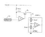
図2において、本発明のセンサ電流制御回路は、狭い応動範囲(たとえば、0V+1.5V〜Vcc−1.5V)を有する一般的なオペアンプを用いたオペアンプA1を備えたハイサイド定電流駆動回路を構成しており、オペアンプA1の反転入力端子は、電流検出抵抗Rcs、抵抗Ruを介して電源Vccに接続され、非反転入力端子は、電源Vccに接続された基準電圧源−Vrefに接続されている。また、オペアンプA1の反転入力端子は、制御電圧源Vaにも接続されている。
【0057】
オペアンプAの出力端子には、抵抗R6を介してPNP型トランジスタQ2のベースが接続されている。PNP型トランジスタQ2のコレクタは接地され、エミッタは、抵抗R7を介して電源Vccに接続されると共にPNP型トランジスタQ1のベースに接続されている。PNP型トランジスタQ1のエミッタは電流検出抵抗Rcsと抵抗Ruの接続点に接続されている。PNP型トランジスタQ1のコレクタと接地間には、負荷RLが接続されている。
【0058】
抵抗R6,R7およびPNP型トランジスタQ2は、図1におけるダイオードD1,D2に相当するものである。
【0059】
制御電圧源Vaは、オペアンプA3と、NPN型トランジスタQ3,Q4と、抵抗R1,R2,R3,R4,R5とからなる。NPN型トランジスタQ3のコレクタは、オペアンプA1の反転入力端子に接続され、ベースは、オペアンプA3の反転入力端子に接続されると共に抵抗R5を介して接地されている。オペアンプA3の非反転入力端子は、基準電圧が供給されている。スイッチング手段としてのNPN型トランジスタQ4のコレクタは抵抗R4を介してNPN型トランジスタQ3のエミッタに接続され、エミッタは接地されて、ベースは、電源Vccと接地間に直列接続された抵抗R1,R2,R3からなる抵抗分圧回路の抵抗R2およびR3の接続点に接続されている。抵抗分圧回路の抵抗R1,R2の接続点に制御信号が供給される。オペアンプA3、NPN型トランジスタQ4および抵抗R5は、定電流駆動回路を構成しており、抵抗R5は定電流駆動回路の電流検出抵抗として作用する。
【0060】
この回路では、特に制御電圧源Vaの構成に特徴があり、以下にその動作を説明する。
【0061】
そこで、ガスセンサRsnsに、通常時の負荷電流IL1と加熱時(検知時)の負荷電流IL2を流す場合を考える。ガスセンサRsnsに通常時の負荷電流IL1を流す場合、抵抗分圧回路の抵抗R1,R2の接続点にハイレベルの制御信号が入力される。この場合、抵抗分圧回路のR2,R3の接続点の分圧電圧によりNPN型トランジスタQ4はONとなり、抵抗R4が抵抗R5に並列接続された状態となる。このときの抵抗R4と抵抗R5の並列抵抗値をRaとする。
【0062】
次に、ガスセンサRsnsに加熱時の負荷電流IL2を流す場合、抵抗分圧回路の抵抗R1,R2の接続点にローレベルの制御信号が入力される。この場合、抵抗分圧回路のR2,R3の接続点の分圧電圧が下がることによりNPN型トランジスタQ4はOFFとなり、抵抗R4が抵抗R5に並列接続されない状態となる。このときの抵抗R5の抵抗値をRbとすると、Ra<Rbとなる。
【0063】
このように、抵抗分圧回路の抵抗R1,R2の接続点に入力されるハイまたはローレベルの制御信号によって、スイッチング手段としてのNPN型トランジスタQ4と抵抗R4の直列接続からなる回路Rxは、電流検出抵抗として働く抵抗R5の抵抗値を可変する可変手段として作用し、定電流駆動回路の電流検出抵抗の抵抗値がRaまたはRbに可変される。
【0064】
したがって、抵抗R4および抵抗R5の抵抗値を適宜に選択することにより、ガスセンサRsnsに通常時または加熱時の負荷電流IL1およびIL2を流すために、抵抗R4と抵抗R5と並列接続による電流検出抵抗Raまたは抵抗R5単独による電流検出抵抗rbとに可変して、その降下電圧をNPN型トランジスタQ3のコレクタからオペアンプA1の反転入力端子へ供給することによって、オペアンプA1の反転入力端子の電位が、Vcc−Vrefになり(言い換えれば、電流検出抵抗Rcsからの負帰還電圧がオペアンプA1の応動範囲内にシフトされ)、ガスセンサRsnsの仕様に合った通常時負荷電流IL1および加熱時負荷電流IL2を流すように制御することができる。
【0065】
以上のように、本発明の実施の形態について説明したが、本発明はこれに限らず、種々の変形、応用が可能である。
【0066】
たとえば、制御電圧源Vaにおける定電流駆動回路の電流検出抵抗の可変手段としての、スイッチング手段であるNPN型トランジスタQ4と抵抗R4との直列接続からなる回路は、実施の形態では1つだけ示されているが、これに限らず複数設けても良い。
【0067】
また、上述の実施の形態では、電源の基準電位点を電源電圧としてハイサイド側で動作する電流制御回路として構成したが、電源の基準電位点をゼロ電位としてローサイド側で動作する電流制御回路として構成することもできる。
【0068】
また、上述の実施の形態では、負荷RLとしてガスセンサ回路の場合を説明したが、これに限らず種々の負荷の電流制御に実施可能である。
【0069】
【発明の効果】
請求項1記載の発明によれば、レイル・ツー・レイルタイプのオペアンプを使用せず、応動範囲の狭い一般的なオペアンプを使用して、コストが安くかつ精度の高い電流制御回路を得ることができる。
【0071】
また、制御電圧源は、定電圧回路ではなく安価な定電流駆動回路構成とすることができる。また、可変手段によって簡単にオペアンプの他方の入力端子に入力される制御電圧の大きさを可変することができる。
【0072】
請求項2記載の発明によれば、スイッチング手段のON/OFF制御により電流検出抵抗の抵抗値を変え、その結果、簡単にオペアンプの他方の入力端子に入力される制御電圧の大きさを可変することができる。
【図面の簡単な説明】
【図1】 参考例の電流制御回路の回路図である。
【図2】 本発明に係る電流制御回路の実施の形態の構成例を示す回路図である。
【図3】 従来の電流制御回路の一例を示す回路図である。
【符号の説明】
Rcs 電流検出抵抗(負荷電流検出手段)
A1 オペアンプ(第1のオペアンプ)
RL 負荷(ガスセンサ回路)
Vcc 電源
Vref 基準電圧源
Va 制御電圧源
CD 定電流駆動回路
R4 抵抗
R5 抵抗(電流検出抵抗)
A3 オペアンプ(第2のオペアンプ)
Rx 可変手段
Q4 NPN型トランジスタ(スイッチング手段)[0001]
BACKGROUND OF THE INVENTION
The present invention relates to a current control circuit, and more particularly to a current control circuit useful for a catalytic combustion type gas sensor circuit.
[0002]
[Prior art]
The applicant has already proposed JP-A-9-318584 as a patent application relating to a current control circuit useful for a catalytic combustion type gas sensor circuit. In Japanese Unexamined Patent Publication No. 9-318584, in catalytic combustion type gas sensor constant current drive circuit used in the negative feedback control operational amplifier, by the apply a constant voltage from the DC power supply positive terminal to the non-inverting input terminal of said operational amplifier A highly reliable catalytic combustion type gas sensor constant current drive circuit that does not cause malfunction even if there is a fluctuation in the DC power supply voltage is disclosed.
[0003]
FIG. 3 is a circuit diagram showing an example of a current control circuit used in a conventional catalytic combustion gas sensor circuit. In FIG. 3, the sensor current control circuit constitutes a high-side constant current drive circuit including an operational amplifier (operational amplifier) A1, and the inverting input terminal of the operational amplifier A1 is connected to the power source Vcc via the current detection resistor Rcs. The non-inverting input terminal is connected to the control voltage Vc. The output terminal of the operational amplifier A1 is connected to the base of the PNP transistor Q1, and the negative input terminal is connected to the emitter of the PNP transistor Q1. A load RL is connected between the collector of the PNP transistor Q1 and the ground.
[0004]
The load RL is a contact combustion type gas sensor circuit, and is connected to a series connection point of the temperature compensation element Rref and the contact combustion type gas sensor Rsns connected in series between the collector of the PNP transistor Q1 and the ground, and the temperature compensation element Rref and the gas sensor Rsns. The operational amplifier A2 is connected to an inverting input terminal. A reference voltage is input to the non-inverting input terminal of the operational amplifier A2.
[0005]
In the load RL, that is, the catalytic combustion type gas sensor circuit, a constant current is supplied to the gas sensor Rsns from the power source Vcc through the current detection resistor Rcs, the transistor Q1, and the temperature compensation element Ref. The operational amplifier A2 compares the constant current input to the inverting input terminal with the voltage drop of the gas sensor Rsns due to the resistance of the gas sensor Rsns and the reference voltage input to the non-inverting input terminal. An output signal is generated at the output terminal, and an alarm buzzer, a display device, etc. (not shown) connected to the subsequent stage are driven to notify that gas has been detected.
[0006]
The contact combustion gas sensor Rsns needs to pass a normal current (idle time) current and a heating (detection time) current determined by the sensor specifications. Therefore, the normal load current IL1 to be passed through the catalytic combustion gas sensor Rsns and the load current IL2 (IL1 <IL2) during heating (detection) are detected by the current detection resistor Rcs. The current detection voltage of the current detection resistor Rcs, that is, the voltage drop is input as a negative feedback voltage to the inverting input terminal of the operational amplifier A1.
[0007]
The operational amplifier A1 provides negative feedback so that the negative feedback voltage supplied to the inverting input terminal, that is, (power supply voltage Vcc−drop voltage Vcs of the current detection resistor Rcs) becomes equal to the control voltage Va input to the non-inverting input terminal. Be controlled.
[0008]
Therefore, the control voltage Va1 corresponding to when the catalytic combustion gas sensor Rsns is in the normal state or the control voltage Va2 corresponding to the heating state is input to the non-inverting input terminal of the operational amplifier A1 as the control voltage Va. The control voltages Va1 and Va2 have different values, specifically, Va1> Va2.
[0009]
[Problems to be solved by the invention]
When a general operational amplifier is used as the operational amplifier A1, the input / output response range is 0V + 1.5V to Vcc−1.5V. That is, a general operational amplifier has a voltage range from the high-side power supply voltage side to a voltage value lowered to 1.5 volt and a voltage range from the low-side zero volt side to a voltage value up to 1.5 volt. Cannot be used in the voltage range.
[0010]
Specific operating conditions of the above-described current control circuit include, for example, a power supply voltage Vcc: +5 V, a load resistance RL: about 12Ω, a current detection resistor Rcs: 2.5Ω, and a normal load current that should flow through the contact combustion gas sensor Rsns. Consider a case where IL1: 170 mA and load current IL2 at heating (detection) IL2: 265 mA. In this case, when the load current IL is 265 mA, the voltage across the load RL rises to about 3.2 V. Therefore, the resistance value of the current detection resistor Rcs is increased and the voltage Vcs input to the inverting input terminal of the operational amplifier A1 is It cannot be lowered below Vcc-1.5V within the response range. Therefore, under such operating conditions, a general operational amplifier cannot be used as the operational amplifier A1 because it does not fall within the response range of a general operational amplifier.
[0011]
For the above-described reason, in this current control circuit example, it is necessary to use a Rail-to-Rail type operational amplifier as the operational amplifier A1. Rail-to-rail type operational amplifiers have a wide response range from the power supply voltage to almost zero volts, so operation within the response range is possible without increasing the resistance value of the current detection resistor Rcs. It becomes.
As described above, in the current control on the high potential (high side) side, when operating a voltage exceeding Vcc-1.5 V (that is, a voltage closer to Vcc than Vcc-1.5 V), an operational amplifier that performs control The operation is ensured by using a Rail to Rail type A1.
[0012]
However, since the rail-to-rail type operational amplifier is expensive in comparison with the general operational amplifier whose response range is 0V + 1.5V to Vcc−1.5V, the cost of the entire current control circuit is low. There is a problem of being up.
[0013]
Therefore, when dealing with operating voltages that do not fall within the operational range of a general operational amplifier, the applicant has already developed a technology that makes it possible to use a general operational amplifier without using a rail-to-rail type operational amplifier. Proposed as Kaihei 9-318583. The technique described in Japanese Patent Laid-Open No. 9-318583 is a floating return that shifts a signal source voltage to the operational range of the operational amplifier in an operational amplifier device in which the signal source voltage used as the input signal of the operational amplifier can be an operating voltage that is lower than the operational range of the operational amplifier. It is configured to add a potential supply circuit, and by shifting the signal source voltage within the response range of the operational amplifier, it is possible to respond to a signal in a wide range even if a conventional operational amplifier with a narrow response range is used. It is.
[0014]
However, the technique described above shifts the input signal source voltage so as to correspond to the response range on the input side of the operational amplifier. However, the operational amplifier to which the negative feedback voltage from the load current detecting means is input is used for the load. In a current control circuit for controlling the load current to be supplied, it is necessary to consider the response range of the operational amplifier according to the load current value on the output side rather than the input side.
[0015]
The object of the present invention is to solve the above-mentioned problems, and does not use a rail-to-rail type operational amplifier, but uses a general operational amplifier with a narrow response range, and is different from the technique previously proposed by the applicant. An object is to provide a current control circuit having a novel configuration.
[0016]
[Means for Solving the Problems]
In view of the above object, the present invention according to claim 1 controls the load current supplied to the load by using the first operational amplifier in which the negative feedback voltage from the load current detecting means is inputted to one input terminal. A current control circuit, connected to the other input terminal of the first operational amplifier, a reference voltage source that applies a reference voltage within a response range of the first operational amplifier as viewed from the reference potential point of the power supply; A control voltage source that provides a control voltage for shifting the negative feedback voltage from the load current detection means within the response range of the first operational amplifier is connected to the input terminal, and the control voltage source has a current connected to one input terminal. It is characterized by comprising a constant current drive circuit including a second operational amplifier to which a negative feedback voltage from the detection resistor is input and variable means for changing the resistance value of the current detection resistor .
[0017]
According to the first aspect of the present invention, in the current control circuit for controlling the load current supplied to the load using the first operational amplifier in which the negative feedback voltage from the load current detecting means is input to one input terminal, A reference voltage source that applies a reference voltage within the response range of the first operational amplifier as viewed from the reference potential point of the power supply is connected to the other input terminal of the operational amplifier. In addition, a control voltage source that provides a control voltage for shifting the negative feedback voltage from the load current detection means within the response range of the first operational amplifier is connected to one input terminal of the first operational amplifier . Since it comprises a constant current drive circuit including a second operational amplifier in which a negative feedback voltage from the current detection resistor is input to one input terminal and a variable means for changing the resistance value of the current detection resistor , Even a narrow general-purpose operational amplifier can be used. Further, the magnitude of the control voltage input to the other input terminal of the first operational amplifier can be easily changed by the variable means.
[0022]
According to a second aspect of the invention, the current control circuit of claim 1, wherein the variable means is connected in parallel with the current detection resistor, characterized in that it comprises at least one circuit comprising a series connection of a resistor and a switching means And
[0023]
According to a second aspect of the present invention, the variable means includes at least one circuit including a series connection of a resistor and a switching means connected in parallel with the current detection resistor, and the current detection resistor is controlled by ON / OFF control of the switching means. As a result, the magnitude of the control voltage input to the other input terminal of the first operational amplifier can be easily varied.
[0026]
DETAILED DESCRIPTION OF THE INVENTION
Hereinafter, embodiments of a current control circuit according to the present invention will be described . First, a reference current control circuit useful for understanding the gist of the current control circuit of the present invention will be described.
[0027]
As shown in FIG. 1, the sensor current control circuit of the reference example has a high-side constant current including an operational amplifier A1 using a general operational amplifier having a narrow response range (for example, 0 V + 1.5 V to Vcc-1.5 V). The inverting input terminal of the operational amplifier A1 is connected to the power supply Vcc via the current detection resistor Rcs and the resistor Ru, and the non-inverting input terminal is connected to the reference voltage source −Vref connected to the power supply Vcc. It is connected. The inverting input terminal of the operational amplifier A1 is also connected to the control voltage source Va via the resistor Rw. The base of the PNP transistor Q1 is connected to the output terminal of the operational amplifier A through diodes D1 and D2. The emitter of the PNP transistor Q1 is connected to the connection point between the current detection resistor Rcs and the resistor Ru. A load RL is connected between the collector of the PNP transistor Q1 and the ground.
[0028]
The load RL is a contact combustion type gas sensor circuit, and is connected to a series connection point of the temperature compensation element Rref and the contact combustion type gas sensor Rsns connected in series between the collector of the PNP transistor Q1 and the ground, and the temperature compensation element Rref and the gas sensor Rsns. The operational amplifier A2 is connected to an inverting input terminal. A reference voltage is input to the non-inverting input terminal of the operational amplifier A2.
[0029]
In the load RL, that is, the catalytic combustion type gas sensor circuit, a constant current is supplied to the gas sensor Rsns from the power source Vcc through the current detection resistor Rcs, the transistor Q1, and the temperature compensation element Ref. The operational amplifier A2 compares the constant current input to the inverting input terminal with the voltage drop of the gas sensor Rsns due to the resistance of the gas sensor Rsns and the reference voltage input to the non-inverting input terminal. An output signal is generated at the output terminal, and an alarm buzzer, a display, etc. (not shown) connected to the subsequent stage are driven by this output signal to notify that gas has been detected.
[0030]
The current detection resistor Rcs detects a normal load current IL1 to be passed through the catalytic combustion gas sensor Rsns and a load current IL2 during heating (detection). The current detection voltage of the current detection resistor Rcs, that is, the voltage drop is input as a negative feedback voltage to the inverting input terminal of the operational amplifier A1 via the resistor Ru.
[0031]
The operational amplifier A1 has a voltage supplied to the inverting input terminal, that is, (a power supply voltage Vcc−a voltage drop Vcs of the current detection resistor Rcs−a voltage drop of the resistor Ru), a voltage input to the non-inverting input terminal, that is, Vcc−Vref. Negative feedback control is performed so that
[0032]
Therefore, the reference voltage source -Vref is a reference voltage applied to the non-inverting input terminal of the operational amplifier A1, that is, Vcc-Vref is a voltage within the operating range of the operational amplifier A1 in view of the reference potential point of the power supply Vcc, here the power supply voltage. Is set to a voltage value.
[0033]
The control voltage source Va is set to a control voltage Va1 corresponding to when the catalytic combustion type gas sensor Rsns is in a normal state or a control voltage Va2 corresponding to when the catalytic combustion gas sensor Rsns is in a heating state (here, Va1> Va2).
[0034]
Therefore, a case is considered in which a normal load current IL1 and a heating (detection) load current IL2 flow through the gas sensor Rsns.
First, when a normal load current IL1 is passed through the gas sensor Rsns, assuming that the voltage drop across the current detection resistor Rcs is Vcs1, and the current flowing through the resistors Ru and Rw is Ia1,
[0035]
Ia1 = (Vcs1-Vref) / Ru (1)
[0036]
The set voltage Va1 when the normal load current IL1 flows through the gas sensor Rsns in the control voltage source Va is
[0037]
Va1 = Vref−Ia1 × Rw (2)
It becomes.
[0038]
Next, when the load current IL2 at the time of heating is passed through the gas sensor Rsns, assuming that the voltage drop across the current detection resistor Rcs is Vcs2, and the current flowing through the resistors Ru and Rw is Ia2.
[0039]
Ia2 = (Vcs2-Vref) / Ru (3)
[0040]
Thus, in the control voltage source Va, the set voltage Va2 when the load current IL1 during heating is passed through the gas sensor Rsns is as follows:
[0041]
Va2 = Vref−Ia2 × Rw (4)
It becomes.
[0042]
The relationship between the resistance values of the resistors Ru and Rw and the resistance value of the current detection resistor Rcs so that the current Ia (Ia1, Ia2) flowing through the resistors Ru and Rw does not affect the load current IL (IL1, IL2). Must be set to satisfy Rcs << Ru, Rw.
[0043]
Thus, by setting the control voltage of the control voltage source Va to Va1 and Va2 in accordance with the normal operation and the heating operation of the gas sensor Rsns, respectively, the potential of the inverting input terminal of the operational amplifier A1 becomes Vcc−Vref. (In other words, the negative feedback voltage from the current detection resistor Rcs is shifted into the response range of the operational amplifier A1), and control is performed so that the normal load current IL1 and the heating load current IL2 that meet the specifications of the gas sensor Rsns flow. Can do.
[0044]
Next, an example of specific operating conditions of this current control circuit will be described. For example, power supply voltage Vcc: +5 V, load resistance RL: about 12Ω, current detection resistance Rcs: 2.5Ω, resistance Ru: 20 kΩ, resistance Rw: 5 kΩ, normal load current IL1: 170 mA and heating of contact combustion type gas sensor Rsns Consider a case where the load current IL2 is 265 mA.
[0045]
In this case, first, a general operational amplifier (for example, one having an input / output response range of 0 V + 1.5 V to Vcc-1.5 V) is used as the operational amplifier A1, and the high-side power supply voltage is applied to the non-inverting input terminal of the operational amplifier A1. In order to supply a voltage value that is a voltage within the response range of the operational amplifier A1 from the 5.0V side, the voltage value of the reference voltage source -Vref may be -1.75V (minimum may be -1.5V). , Taking into account tolerances). Therefore, the reference voltage of Vcc−Vref = 5.0−1.75 = 3.25 volts is supplied to the non-inverting input terminal of the operational amplifier A1.
[0046]
Therefore, when the normal load current IL1: 170 mA of the contact combustion type gas sensor Rsns is passed, the current Ia1 flowing through the resistor Ru can be obtained from the above equation (1) as follows.
[0047]
Ia1 = (− 0.425V − (− 1.75V)) / 20000 = 66.25 μA
[0048]
The set voltage Va1 for allowing the normal load current IL1 of the gas sensor Rsns to flow in the control voltage source Va is obtained as follows from the above equation (2).
[0049]
Va1 = −1.75V−66.25 μA × 5000 = −2.08125V
[0050]
Next, when the heating load current IL1: 265 mA of the contact combustion type gas sensor Rsns is passed, the current Ia2 flowing through the resistor Ru is obtained as follows from the above equation (3).
[0051]
Ia2 = (− 0.6625V − (− 1.75V)) / 20000 = 54.375 μA
[0052]
The set voltage Va2 for causing the load current IL2 during heating of the gas sensor Rsns to flow in the control voltage source Va is obtained from the above-described equation (4) as follows.
[0053]
Va2 = −1.75V−54.375 μA × 5000 = −2.02185V
[0054]
In this way, by setting the control voltage of the control voltage source Va to −2.08125V and −2.02185V in accordance with the normal operation and the heating operation of the gas sensor Rsns, respectively, the potential of the inverting input terminal of the operational amplifier A1 is set. Vcc−1.75 V (in other words, the negative feedback voltage from the current detection resistor Rcs is shifted into the response range of the operational amplifier A1), the normal load current IL1: 170 mA and the heating load current IL2 of the gas sensor Rsns: It can control to flow 265mA.
[0055]
Next, FIG. 2 is a circuit diagram showing a configuration example of an embodiment of a current control circuit according to the present invention . In FIG. 2, the same components as those in FIG.
[0056]
In FIG. 2, the sensor current control circuit of the present invention includes a high-side constant current drive circuit including an operational amplifier A1 using a general operational amplifier having a narrow response range (for example, 0V + 1.5V to Vcc−1.5V). The inverting input terminal of the operational amplifier A1 is connected to the power supply Vcc via the current detection resistor Rcs and the resistor Ru, and the non-inverting input terminal is connected to the reference voltage source -Vref connected to the power supply Vcc. Yes. The inverting input terminal of the operational amplifier A1 is also connected to the control voltage source Va.
[0057]
The base of a PNP transistor Q2 is connected to the output terminal of the operational amplifier A through a resistor R6. The collector of the PNP transistor Q2 is grounded, and the emitter is connected to the power supply Vcc via the resistor R7 and is connected to the base of the PNP transistor Q1. The emitter of the PNP transistor Q1 is connected to the connection point between the current detection resistor Rcs and the resistor Ru. A load RL is connected between the collector of the PNP transistor Q1 and the ground.
[0058]
The resistors R6 and R7 and the PNP transistor Q2 correspond to the diodes D1 and D2 in FIG.
[0059]
The control voltage source Va includes an operational amplifier A3, NPN transistors Q3 and Q4, and resistors R1, R2, R3, R4 and R5. The collector of the NPN transistor Q3 is connected to the inverting input terminal of the operational amplifier A1, and the base is connected to the inverting input terminal of the operational amplifier A3 and grounded through the resistor R5. A reference voltage is supplied to the non-inverting input terminal of the operational amplifier A3. The collector of the NPN transistor Q4 as a switching means is connected to the emitter of the NPN transistor Q3 via a resistor R4, the emitter is grounded, and the base is a resistor R1, R2, connected in series between the power source Vcc and the ground. It is connected to the connection point of the resistors R2 and R3 of the resistance voltage dividing circuit composed of R3. A control signal is supplied to a connection point between the resistors R1 and R2 of the resistor voltage dividing circuit. The operational amplifier A3, the NPN transistor Q4, and the resistor R5 constitute a constant current drive circuit, and the resistor R5 functions as a current detection resistor of the constant current drive circuit.
[0060]
This circuit is particularly characterized by the configuration of the control voltage source Va, and its operation will be described below.
[0061]
Therefore, a case is considered in which a normal load current IL1 and a heating (detection) load current IL2 flow through the gas sensor Rsns. When the normal load current IL1 is supplied to the gas sensor Rsns, a high-level control signal is input to the connection point between the resistors R1 and R2 of the resistance voltage dividing circuit. In this case, the NPN transistor Q4 is turned on by the divided voltage at the connection point between R2 and R3 of the resistance voltage dividing circuit, and the resistor R4 is connected in parallel to the resistor R5. The parallel resistance value of the resistor R4 and the resistor R5 at this time is represented by Ra.
[0062]
Next, when the load current IL2 during heating is supplied to the gas sensor Rsns, a low-level control signal is input to the connection point between the resistors R1 and R2 of the resistance voltage dividing circuit. In this case, when the divided voltage at the connection point between R2 and R3 of the resistance voltage dividing circuit is lowered, the NPN transistor Q4 is turned OFF, and the resistor R4 is not connected to the resistor R5 in parallel. If the resistance value of the resistor R5 at this time is Rb, then Ra <Rb.
[0063]
As described above, the circuit Rx formed of the serial connection of the NPN transistor Q4 as the switching means and the resistor R4 is controlled by the high or low level control signal input to the connection point between the resistors R1 and R2 of the resistor voltage dividing circuit. Acting as a variable means for varying the resistance value of the resistor R5 acting as a detection resistor, the resistance value of the current detection resistor of the constant current drive circuit is varied to Ra or Rb.
[0064]
Therefore, by appropriately selecting the resistance values of the resistor R4 and the resistor R5, in order to cause the load currents IL1 and IL2 during normal or heating to flow through the gas sensor Rsns, the current detection resistor Ra in parallel connection with the resistor R4 and the resistor R5. Alternatively, the voltage is changed to the current detection resistor rb by the resistor R5 alone, and the voltage drop is supplied from the collector of the NPN transistor Q3 to the inverting input terminal of the operational amplifier A1, so that the potential of the inverting input terminal of the operational amplifier A1 becomes Vcc−. Vref (in other words, the negative feedback voltage from the current detection resistor Rcs is shifted into the response range of the operational amplifier A1) so that the normal load current IL1 and the heating load current IL2 that meet the specifications of the gas sensor Rsns flow. Can be controlled.
[0065]
As described above, has been described with reference to the embodiments of the present invention, the present invention is not limited thereto, and various modifications, Ru applications can der.
[0066]
For example, in the embodiment, only one circuit including a series connection of an NPN transistor Q4, which is a switching means, and a resistor R4 as a variable means of a current detection resistor of a constant current driving circuit in the control voltage source Va is shown. However, the present invention is not limited to this, and a plurality of them may be provided.
[0067]
In the above-described embodiment, the current control circuit is configured to operate on the high side with the reference potential point of the power supply as the power supply voltage. However, the current control circuit operates on the low side with the reference potential point of the power supply as the zero potential. It can also be configured.
[0068]
In the above-described embodiment, the case of the gas sensor circuit as the load RL has been described. However, the present invention is not limited to this and can be implemented for current control of various loads.
[0069]
【The invention's effect】
According to the first aspect of the present invention, it is possible to obtain a current control circuit with low cost and high accuracy by using a general operational amplifier having a narrow response range without using a rail-to-rail type operational amplifier. it can.
[0071]
Further, the control voltage source can be an inexpensive constant current drive circuit configuration instead of a constant voltage circuit. In addition, the magnitude of the control voltage input to the other input terminal of the operational amplifier can be easily changed by the variable means.
[0072]
According to the second aspect of the present invention, the resistance value of the current detection resistor is changed by ON / OFF control of the switching means, and as a result, the magnitude of the control voltage input to the other input terminal of the operational amplifier is easily varied. be able to.
[Brief description of the drawings]
FIG. 1 is a circuit diagram of a current control circuit of a reference example.
FIG. 2 is a circuit diagram showing a configuration example of an embodiment of a current control circuit according to the present invention .
FIG. 3 is a circuit diagram showing an example of a conventional current control circuit.
[Explanation of symbols]
Rcs Current detection resistor (load current detection means)
A1 operational amplifier (first operational amplifier)
RL load (gas sensor circuit)
Vcc power supply Vref reference voltage source Va control voltage source CD constant current drive circuit R4 resistor R5 resistor (current detection resistor)
A3 operational amplifier (second operational amplifier)
Rx variable means Q4 NPN transistor (switching means)
Claims (2)
上記第1のオペアンプの他方の入力端子に、電源の基準電位点からみて上記第1のオペアンプの応動範囲内の基準電圧を与える基準電圧源を接続し、上記一方の入力端子に、上記負荷電流検出手段からの負帰還電圧を上記第1のオペアンプの応動範囲内にシフトさせる制御電圧を与える制御電圧源を接続し、
上記制御電圧源は、一方の入力端子に電流検出抵抗からの負帰還電圧が入力される第2のオペアンプと、上記電流検出抵抗の抵抗値を可変する可変手段とを含む定電流駆動回路で構成される
ことを特徴とする電流制御回路。A current control circuit for controlling a load current supplied to a load using a first operational amplifier in which a negative feedback voltage from a load current detection means is input to one input terminal;
A reference voltage source that applies a reference voltage within a response range of the first operational amplifier as viewed from a reference potential point of a power supply is connected to the other input terminal of the first operational amplifier, and the load current is connected to the one input terminal. Connecting a control voltage source for providing a control voltage for shifting the negative feedback voltage from the detection means within the response range of the first operational amplifier ;
The control voltage source includes a constant current drive circuit including a second operational amplifier in which a negative feedback voltage from a current detection resistor is input to one input terminal, and a variable unit that varies the resistance value of the current detection resistor. current control circuit, characterized in that the.
ことを特徴とする請求項1記載の電流制御回路。 2. The current control circuit according to claim 1 , wherein the variable means includes at least one circuit composed of a series connection of a resistor and a switching means connected in parallel with the current detection resistor .
Priority Applications (1)
| Application Number | Priority Date | Filing Date | Title |
|---|---|---|---|
| JP37476299A JP3750911B2 (en) | 1999-12-28 | 1999-12-28 | Current control circuit |
Applications Claiming Priority (1)
| Application Number | Priority Date | Filing Date | Title |
|---|---|---|---|
| JP37476299A JP3750911B2 (en) | 1999-12-28 | 1999-12-28 | Current control circuit |
Publications (2)
| Publication Number | Publication Date |
|---|---|
| JP2001188617A JP2001188617A (en) | 2001-07-10 |
| JP3750911B2 true JP3750911B2 (en) | 2006-03-01 |
Family
ID=18504390
Family Applications (1)
| Application Number | Title | Priority Date | Filing Date |
|---|---|---|---|
| JP37476299A Expired - Fee Related JP3750911B2 (en) | 1999-12-28 | 1999-12-28 | Current control circuit |
Country Status (1)
| Country | Link |
|---|---|
| JP (1) | JP3750911B2 (en) |
Families Citing this family (3)
| Publication number | Priority date | Publication date | Assignee | Title |
|---|---|---|---|---|
| CN1296705C (en) * | 2003-06-11 | 2007-01-24 | 宇东科技股份有限公司 | Control circuit for adjustable biological sensor and measuring method thereof |
| KR101611842B1 (en) | 2014-05-15 | 2016-04-12 | 우석대학교 산학협력단 | A circuit for controlling current |
| CN115268558B (en) * | 2022-08-22 | 2024-03-22 | 苏州智而卓数字科技有限公司 | Universal output interface circuit for voltage and current |
-
1999
- 1999-12-28 JP JP37476299A patent/JP3750911B2/en not_active Expired - Fee Related
Also Published As
| Publication number | Publication date |
|---|---|
| JP2001188617A (en) | 2001-07-10 |
Similar Documents
| Publication | Publication Date | Title |
|---|---|---|
| JP3240216B2 (en) | Detection circuit, device and power supply circuit for detecting voltage fluctuation with respect to set value | |
| EP0419093A2 (en) | Current sensing circuit | |
| JP2643813B2 (en) | Stabilized power supply circuit | |
| EP0493750B1 (en) | A comparator circuit with precision hysteresis and high input impedance | |
| KR930023800A (en) | Anomaly Detection Circuit of Temperature Sensor | |
| JP3750911B2 (en) | Current control circuit | |
| JP2002017036A (en) | Over-current detection circuit | |
| JPH01212364A (en) | Load current detection circuit | |
| US5750893A (en) | Thermally sensing type flowing velocity measuring apparatus | |
| JP4375025B2 (en) | Output circuit and operational amplifier | |
| JP3330004B2 (en) | DC stabilized power supply | |
| JP2001108712A (en) | Current detector | |
| JP3239052B2 (en) | Semiconductor integrated circuit | |
| JP3158449B2 (en) | Voltage detection circuit | |
| JP3547042B2 (en) | Control circuit of catalytic combustion type gas sensor | |
| JP3203521B2 (en) | Load disconnection detection circuit | |
| JP2800225B2 (en) | Constant voltage power supply circuit | |
| JP3098451B2 (en) | Amplifier circuit | |
| JP3003455B2 (en) | Overheat detection circuit | |
| JP3343833B2 (en) | Power amplifier | |
| JPH1151792A (en) | Sensor signal circuit | |
| JP2548022Y2 (en) | Stabilized power supply circuit | |
| JP2714151B2 (en) | Current limit circuit | |
| JP4258837B2 (en) | 2-wire transmission circuit | |
| JP3063345B2 (en) | Saturation prevention circuit |
Legal Events
| Date | Code | Title | Description |
|---|---|---|---|
| A977 | Report on retrieval |
Free format text: JAPANESE INTERMEDIATE CODE: A971007 Effective date: 20050126 |
|
| A131 | Notification of reasons for refusal |
Free format text: JAPANESE INTERMEDIATE CODE: A131 Effective date: 20050201 |
|
| A131 | Notification of reasons for refusal |
Free format text: JAPANESE INTERMEDIATE CODE: A131 Effective date: 20050823 |
|
| A521 | Written amendment |
Free format text: JAPANESE INTERMEDIATE CODE: A523 Effective date: 20051017 |
|
| TRDD | Decision of grant or rejection written | ||
| A01 | Written decision to grant a patent or to grant a registration (utility model) |
Free format text: JAPANESE INTERMEDIATE CODE: A01 Effective date: 20051122 |
|
| RD01 | Notification of change of attorney |
Free format text: JAPANESE INTERMEDIATE CODE: A7426 Effective date: 20051202 |
|
| RD03 | Notification of appointment of power of attorney |
Free format text: JAPANESE INTERMEDIATE CODE: A7423 Effective date: 20051202 |
|
| A61 | First payment of annual fees (during grant procedure) |
Free format text: JAPANESE INTERMEDIATE CODE: A61 Effective date: 20051202 |
|
| R150 | Certificate of patent or registration of utility model |
Ref document number: 3750911 Country of ref document: JP Free format text: JAPANESE INTERMEDIATE CODE: R150 Free format text: JAPANESE INTERMEDIATE CODE: R150 |
|
| FPAY | Renewal fee payment (event date is renewal date of database) |
Free format text: PAYMENT UNTIL: 20081216 Year of fee payment: 3 |
|
| FPAY | Renewal fee payment (event date is renewal date of database) |
Free format text: PAYMENT UNTIL: 20091216 Year of fee payment: 4 |
|
| FPAY | Renewal fee payment (event date is renewal date of database) |
Free format text: PAYMENT UNTIL: 20101216 Year of fee payment: 5 |
|
| FPAY | Renewal fee payment (event date is renewal date of database) |
Free format text: PAYMENT UNTIL: 20101216 Year of fee payment: 5 |
|
| FPAY | Renewal fee payment (event date is renewal date of database) |
Free format text: PAYMENT UNTIL: 20111216 Year of fee payment: 6 |
|
| FPAY | Renewal fee payment (event date is renewal date of database) |
Free format text: PAYMENT UNTIL: 20111216 Year of fee payment: 6 |
|
| FPAY | Renewal fee payment (event date is renewal date of database) |
Free format text: PAYMENT UNTIL: 20121216 Year of fee payment: 7 |
|
| FPAY | Renewal fee payment (event date is renewal date of database) |
Free format text: PAYMENT UNTIL: 20121216 Year of fee payment: 7 |
|
| S111 | Request for change of ownership or part of ownership |
Free format text: JAPANESE INTERMEDIATE CODE: R313111 |
|
| FPAY | Renewal fee payment (event date is renewal date of database) |
Free format text: PAYMENT UNTIL: 20121216 Year of fee payment: 7 |
|
| R350 | Written notification of registration of transfer |
Free format text: JAPANESE INTERMEDIATE CODE: R350 |
|
| FPAY | Renewal fee payment (event date is renewal date of database) |
Free format text: PAYMENT UNTIL: 20121216 Year of fee payment: 7 |
|
| FPAY | Renewal fee payment (event date is renewal date of database) |
Free format text: PAYMENT UNTIL: 20131216 Year of fee payment: 8 |
|
| R250 | Receipt of annual fees |
Free format text: JAPANESE INTERMEDIATE CODE: R250 |
|
| R250 | Receipt of annual fees |
Free format text: JAPANESE INTERMEDIATE CODE: R250 |
|
| R250 | Receipt of annual fees |
Free format text: JAPANESE INTERMEDIATE CODE: R250 |
|
| LAPS | Cancellation because of no payment of annual fees |