JP3738331B2 - LCD module - Google Patents
LCD module Download PDFInfo
- Publication number
- JP3738331B2 JP3738331B2 JP29791096A JP29791096A JP3738331B2 JP 3738331 B2 JP3738331 B2 JP 3738331B2 JP 29791096 A JP29791096 A JP 29791096A JP 29791096 A JP29791096 A JP 29791096A JP 3738331 B2 JP3738331 B2 JP 3738331B2
- Authority
- JP
- Japan
- Prior art keywords
- flexible wiring
- wiring board
- liquid crystal
- shield case
- crystal display
- Prior art date
- Legal status (The legal status is an assumption and is not a legal conclusion. Google has not performed a legal analysis and makes no representation as to the accuracy of the status listed.)
- Expired - Fee Related
Links
Images


Landscapes
- Liquid Crystal (AREA)
- Devices For Indicating Variable Information By Combining Individual Elements (AREA)
Description
【0001】
【発明の属する技術分野】
この発明は液晶表示モジュールに関する。
【0002】
【従来の技術】
図6〜図8は液晶表示モジュールの一例を示したものである。このうち図6は液晶表示モジュールの平面図を示し、図7は図6において上側のシールドケースを取り除いた状態の平面図を示し、図8は図6のA−A線に沿う断面図を示す。この液晶表示モジュールは、液晶表示パネル1、LSIチップ等からなる3つの半導体チップ2〜4、フレキシブル配線基板5、金属製の一対のシールドケース6、7を備えている。液晶表示パネル1は、ガラス等からなる2枚の透明基板8、9間に液晶(図示せず)が封入され、透明基板8、9の下面および上面に偏光板10が貼り付けられた構造となっている。この場合、下側の透明基板8の手前側および右側の2辺は上側の透明基板9のそれぞれ対応する手前側および右側の2辺から突出され、L字状の突出部11が形成されている。所定の2つの半導体チップ2、3は突出部11の一端部側の上面に搭載され、残りの1つの半導体チップ4は突出部11の他端部側の上面に搭載されている。フレキシブル配線基板5はベースフィルム5aと、ベースフィルム5aの下面の幅方向両端部を除く部分に設けられた配線5bと、配線5bを含むベースフィルム5aの下面に設けられた保護膜5cとからなっている。フレキシブル配線基板5の一端部は液晶表示パネル1の突出部11の一端部と他端部との交差部分に接続されている。そして、液晶表示パネル1は、液晶表示パネル1の表示領域1aに対応する部分にそれぞれ開口部12が設けられた下側のシールドケース6と上側のシールドケース7との間に収納されている。この場合、下側のシールドケース6と上側のシールドケース7とは、下側のシールドケース6の側壁6aが上側のシールドケース7の側壁7a内に嵌合され、図示しないフック部によって互いに結合されている。
【0003】
ところで、フレキシブル配線基板5の他端部側はシールドケース6、7の右手前側における両シールドケース6、7の間から引き出されている。このシールドケース6、7におけるフレキシブル配線基板5の引き出し部分であって両シールドケース6、7の端部には、製造工程等においてフレキシブル配線基板5が折り曲げられたとき、シールドケース6、7の端部によってフレキシブル配線基板5の配線5bが損傷しないようにそれぞれ受け部13、14が設けられている。この場合、下側のシールドケース6の受け部13は断面U字状をなして下側のシールドケース6の端部から突出され、上側のシールドケース7の受け部14は断面L字状をなして上側のシールドケース7の端部から突出されている。
【0004】
【発明が解決しようとする課題】
しかしながら、従来のこのような液晶表示モジュールでは、シールドケース6、7におけるフレキシブル配線基板5の引き出し部分にシールドケース6、7の端部から受け部13、14が突設され、特に下側のシールドケース6の受け部13は下側のシールドケース6の外形からさらに突出しているので、金属板を打抜いてシールドケース6、7を形成する際に材料が無駄になり、材料費がかかり、コスト高になるという問題があった。
この発明の課題は、コストを低減することができるようにすることである。
【0005】
【課題を解決するための手段】
この発明は、液晶表示パネルと、該液晶表示パネルを収納する一対のシールドケースと、所定の一の面の幅方向両端部を除く部分に配線が設けられ、一端部が前記液晶表示パネルに接続されて前記一対のシールドケースの間から引き出されたフレキシブル配線基板とを備え、前記一対のシールドケースのうちの一方のシールドケースの端面に前記フレキシブル配線基板の幅方向両端部を除く部分に対応する逃げ用凹部と、前記フレキシブル配線基板の幅方向両端部に対応する突起と、が設けられ、前記フレキシブル配線基板の所定の一の面を前記一方のシールドケース側に折り曲げた場合、前記フレキシブル配線基板の幅方向両端部が前記突起に当接し、前記フレキシブル配線基板の所定の一の面の幅方向中央部が前記逃げ用凹部により前記一方のシールドケースの端面に当接しないようにされているものである。
【0006】
この発明によれば、一対のシールドケースのうちの一方のシールドケースの端面にフレキシブル配線基板の幅方向両端部を除く部分に対応する逃げ用凹部と、前記フレキシブル配線基板の幅方向両端部に対応する突起と、が設けられ、フレキシブル配線基板の所定の一の面を前記一方のシールドケース側に折り曲げた場合、前記フレキシブル配線基板の所定の一の面の幅方向両端部が突起に当接し、フレキシブル配線基板の所定の一の面の幅方向中央部が逃げ用凹部により一方のシールドケースの端面に当接しないようにされているので、フレキシブル配線基板の配線を一方のシールドケースの端部によって損傷させないようにすることができ、従来のようにフレキシブル配線基板の受け部をシールドケースに突設する必要がなく、シールドケースを形成するときに材料が無駄になることがなく、コストを低減することができる。
【0007】
【発明の実施の形態】
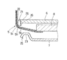
図1〜図4はこの発明の一実施形態における液晶表示モジュールを示したものである。このうち図1は液晶表示モジュールの底面図を示し、図2は図1の一部拡大図を示し、図3(A)は図2のA−A線に沿う断面図を示し、図3(B)は図2のB−B線に沿う断面図を示し、図4は図2のA−A線に沿う断面図を示す。これらの図において、図6および図8と同一部分には同一の符号を付し、その説明を適宜省略する。この実施形態における液晶表示モジュールでは、フレキシブル配線基板5の他端部側がシールドケース6、7の左手前側における両シールドケース6、7の間から引き出されている。シールドケース6、7におけるフレキシブル配線基板5の引き出し部分であって下側のシールドケース(図1〜図4では上側)6の端面には、フレキシブル配線基板5の配線5bに対応する部分、つまりフレキシブル配線基板5の幅方向両端部を除く部分に対応する部分に逃げ用凹部21が設けられ、逃げ用凹部21の両端部、つまりフレキシブル配線基板5の幅方向両端部に対応する部分に突起22が設けられている。この場合、突起22の先端は下側のシールドケース6の端部と同一線上にあり、突起22の突出量、つまり逃げ用凹部21の深さは一例として0.3mm程度となっている。また、シールドケース6、7におけるフレキシブル配線基板5の引き出し部分であって上側のシールドケース(図1〜図4では下側)7の端部は、断面U字状の受け部23となっている。なお、各シールドケース6、7の端部には外側の部分に打抜き時のバリ24、25が形成されている。
【0008】
そして、フレキシブル配線基板5を下側のシールドケース6側に折り曲げた場合、図3(A)および(B)に示すように、フレキシブル配線基板5の幅方向両端部が突起22に当接した状態でフレキシブル配線基板5が折れ曲がり、フレキシブル配線基板5の幅方向中央部が逃げ用凹部21内に位置して、下側のシールドケース6の端面と当接しないので、フレキシブル配線基板5の配線5bが下側のシールドケース6の端部によって損傷することがない。この場合、バリ24は下側のシールドケース6の端部の外側の部分に形成され、フレキシブル配線基板5と接触することがないので、フレキシブル配線基板5の配線5bがバリ24によって損傷することがない。一方、フレキシブル配線基板5を上側のシールドケース7側に折り曲げた場合、図4に示すように、フレキシブル配線基板5が上側のシールドケース7の受け部23に沿って緩やかに折れ曲がるので、フレキシブル配線基板5の配線5bが上側のシールドケース7の端部によって損傷することがない。この場合も、バリ25は上側のシールドケース7の端部の外側の部分に形成され、フレキシブル配線基板5と接触することがないので、フレキシブル配線基板5の配線5bがバリ25によって損傷することがない。
【0009】
このように、この液晶表示モジュールでは、フレキシブル配線基板5の上面の幅方向両端部が下側のシールドケース6の突起22に当接したとき、フレキシブル配線基板5の上面の幅方向中央部が下側のシールドケース6の端面に当接しないように下側のシールドケース6の端面に逃げ用凹部21が設けられているので、フレキシブル配線基板5を下側のシールドケース6側に折り曲げたときにフレキシブル配線基板5の配線5aを下側のシールドケース6の端部によって損傷させないようにすることができ、図8に示す従来のようにフレキシブル配線基板5の受け部13、14をシールドケース6、7に突設する必要がなく、シールドケース6、7を形成するときに材料が無駄になることがなく、コストを低減することができる。
【0010】
なお、上記実施形態では、下側のシールドケース6の外側にバリが形成されていた場合について説明したが、これに限らず、図5に示す変形例のように、下側のシールドケース6の端部の内側の部分にバリ26が形成されていてもよく、この場合には突起22をフレキシブル配線基板5側に起立させればよい。
【0011】
【発明の効果】
以上説明したように、この発明によれば、一対のシールドケースのうちの一方のシールドケースの端面にフレキシブル配線基板の幅方向両端部を除く部分に対応する逃げ用凹部と、前記フレキシブル配線基板の幅方向両端部に対応する突起と、が設けられ、フレキシブル配線基板の所定の一の面を前記一方のシールドケース側に折り曲げた場合、前記フレキシブル配線基板の所定の一の面の幅方向両端部が突起に当接し、フレキシブル配線基板の所定の一の面の幅方向中央部が逃げ用凹部により一方のシールドケースの端面に当接しないようにされているので、フレキシブル配線基板の配線を一方のシールドケースの端部によって損傷させないようにすることができ、従来のようにフレキシブル配線基板の受け部をシールドケースに突設する必要がなく、シールドケースを形成するときに材料が無駄になることがなく、コストを低減することができる。
【図面の簡単な説明】
【図1】この発明の一実施形態における液晶表示モジュールの底面図。
【図2】図1の一部拡大図。
【図3】(A)は図2のA−A線に沿う断面図、(B)は図2のB−B線に沿う断面図。
【図4】図2のA−A線に沿う断面図。
【図5】突起の変形例を示す断面図。
【図6】従来の液晶表示モジュールの平面図。
【図7】同液晶表示モジュールにおいて、上側のシールドケースを取り除いた状態を示す平面図。
【図8】図5のA−A線に沿う断面図。
【符号の説明】
1 液晶表示パネル
5 フレキシブル配線基板
6、7 シールドケース
21 逃げ用凹部
22 突起[0001]
BACKGROUND OF THE INVENTION
The present invention relates to a liquid crystal display module.
[0002]
[Prior art]
6 to 8 show an example of a liquid crystal display module. 6 shows a plan view of the liquid crystal display module, FIG. 7 shows a plan view with the upper shield case removed in FIG. 6, and FIG. 8 shows a cross-sectional view taken along line AA of FIG. . This liquid crystal display module includes a liquid crystal display panel 1, three
[0003]
By the way, the other end side of the
[0004]
[Problems to be solved by the invention]
However, in such a conventional liquid crystal display module, the receiving
An object of the present invention is to enable cost reduction.
[0005]
[Means for Solving the Problems]
In the present invention, a liquid crystal display panel, a pair of shield cases for housing the liquid crystal display panel, and wiring are provided in a portion excluding both ends in the width direction of a predetermined surface, and one end is connected to the liquid crystal display panel And a flexible wiring board drawn out from between the pair of shield cases, the end face of one shield case of the pair of shield cases corresponding to a portion excluding both ends in the width direction of the flexible wiring board. When the escape recess and protrusions corresponding to both ends in the width direction of the flexible wiring board are provided, and the predetermined one surface of the flexible wiring board is bent to the one shield case side, the flexible wiring board Both end portions in the width direction abut against the protrusions, and the central portion in the width direction of the predetermined one surface of the flexible wiring board is formed by the escape recess. Are those not to contact with the end face of the square of the shield case.
[0006]
According to the present invention, the clearance recess corresponding to the portion excluding both ends in the width direction of the flexible wiring board on the end surface of one shield case of the pair of shielding cases, and corresponding to the width direction both ends of the flexible wiring board And when the predetermined one surface of the flexible wiring board is bent to the one shield case side, both end portions in the width direction of the predetermined one surface of the flexible wiring substrate are in contact with the protrusion, Since the central portion in the width direction of the predetermined one surface of the flexible wiring board is prevented from coming into contact with the end surface of one shield case by the recess for escape, the wiring of the flexible wiring substrate is connected by the end portion of one shield case. It can be prevented from being damaged, and it is not necessary to project the receiving part of the flexible wiring board to the shield case as in the conventional case. Without a material is wasted in forming the over scan, the cost can be reduced.
[0007]
DETAILED DESCRIPTION OF THE INVENTION
1 to 4 show a liquid crystal display module according to an embodiment of the present invention. 1 shows a bottom view of the liquid crystal display module, FIG. 2 shows a partially enlarged view of FIG. 1, FIG. 3A shows a cross-sectional view taken along the line AA of FIG. B) shows a cross-sectional view along the line BB in FIG. 2, and FIG. 4 shows a cross-sectional view along the line AA in FIG. In these drawings, the same parts as those in FIGS. 6 and 8 are denoted by the same reference numerals, and the description thereof is omitted as appropriate. In the liquid crystal display module in this embodiment, the other end portion side of the
[0008]
When the
[0009]
As described above, in this liquid crystal display module, when both ends in the width direction of the upper surface of the
[0010]
In the above embodiment, the case where burrs are formed on the outer side of the
[0011]
【The invention's effect】
As described above, according to the present invention, the relief recess corresponding to the portion excluding both ends in the width direction of the flexible wiring board on the end surface of one of the pair of shield cases, and the flexible wiring board Protrusions corresponding to both ends in the width direction, and when the predetermined one surface of the flexible wiring board is bent to the one shield case side, both end portions in the width direction of the predetermined one surface of the flexible wiring board Is in contact with the protrusion, and the central portion in the width direction of the predetermined one surface of the flexible wiring board is prevented from coming into contact with the end surface of one shield case by the recess for escape. It can be prevented from being damaged by the end of the shield case, and the receiving portion of the flexible wiring board is projected from the shield case as in the past. No necessity, without material wasted in forming the shield case, the cost can be reduced.
[Brief description of the drawings]
FIG. 1 is a bottom view of a liquid crystal display module according to an embodiment of the present invention.
2 is a partially enlarged view of FIG.
3A is a cross-sectional view taken along line AA in FIG. 2, and FIG. 3B is a cross-sectional view taken along line BB in FIG.
4 is a cross-sectional view taken along the line AA in FIG.
FIG. 5 is a cross-sectional view showing a modification of the protrusion.
FIG. 6 is a plan view of a conventional liquid crystal display module.
FIG. 7 is a plan view showing a state in which the upper shield case is removed in the liquid crystal display module.
8 is a cross-sectional view taken along line AA in FIG.
[Explanation of symbols]
DESCRIPTION OF SYMBOLS 1 Liquid
Claims (3)
前記一対のシールドケースのうちの一方のシールドケースの端面に前記フレキシブル配線基板の幅方向両端部を除く部分に対応する逃げ用凹部と、前記フレキシブル配線基板の幅方向両端部に対応する突起と、が設けられ、前記フレキシブル配線基板の所定の一の面を前記一方のシールドケース側に折り曲げた場合、前記フレキシブル配線基板の所定の一の面の幅方向両端部が前記突起に当接し、前記フレキシブル配線基板の所定の一の面の幅方向中央部が前記逃げ用凹部により前記一方のシールドケースの端面に当接しないようにされていることを特徴とする液晶表示モジュール。The liquid crystal display panel, a pair of shield cases for storing the liquid crystal display panel, and wirings are provided in portions excluding both ends in the width direction of a predetermined surface, and one end is connected to the liquid crystal display panel and the pair And a flexible wiring board drawn from between the shield cases,
A recess for escape corresponding to a portion excluding both ends in the width direction of the flexible wiring board on the end surface of one shield case of the pair of shield cases, and a protrusion corresponding to both ends in the width direction of the flexible wiring board, When the predetermined one surface of the flexible wiring board is bent to the one shield case side, both end portions in the width direction of the predetermined one surface of the flexible wiring substrate are in contact with the protrusions, and the flexible wiring substrate A liquid crystal display module, wherein a central portion in the width direction of a predetermined surface of the wiring board is not brought into contact with an end surface of the one shield case by the escape recess.
Priority Applications (1)
| Application Number | Priority Date | Filing Date | Title |
|---|---|---|---|
| JP29791096A JP3738331B2 (en) | 1996-10-23 | 1996-10-23 | LCD module |
Applications Claiming Priority (1)
| Application Number | Priority Date | Filing Date | Title |
|---|---|---|---|
| JP29791096A JP3738331B2 (en) | 1996-10-23 | 1996-10-23 | LCD module |
Publications (2)
| Publication Number | Publication Date |
|---|---|
| JPH10123558A JPH10123558A (en) | 1998-05-15 |
| JP3738331B2 true JP3738331B2 (en) | 2006-01-25 |
Family
ID=17852684
Family Applications (1)
| Application Number | Title | Priority Date | Filing Date |
|---|---|---|---|
| JP29791096A Expired - Fee Related JP3738331B2 (en) | 1996-10-23 | 1996-10-23 | LCD module |
Country Status (1)
| Country | Link |
|---|---|
| JP (1) | JP3738331B2 (en) |
Families Citing this family (3)
| Publication number | Priority date | Publication date | Assignee | Title |
|---|---|---|---|---|
| KR101152125B1 (en) | 2005-05-26 | 2012-06-15 | 삼성전자주식회사 | Display device |
| JP5392866B2 (en) * | 2011-11-15 | 2014-01-22 | 日本電気株式会社 | Frame member |
| CN103365502A (en) * | 2012-03-31 | 2013-10-23 | 浙江金徕镀膜有限公司 | Capacitive touch screen |
-
1996
- 1996-10-23 JP JP29791096A patent/JP3738331B2/en not_active Expired - Fee Related
Also Published As
| Publication number | Publication date |
|---|---|
| JPH10123558A (en) | 1998-05-15 |
Similar Documents
| Publication | Publication Date | Title |
|---|---|---|
| US6611302B1 (en) | Flat panel display device | |
| JP4541317B2 (en) | Liquid crystal display | |
| JP3436240B2 (en) | Flat panel display | |
| CN100397174C (en) | Liquid crystal display apparatus | |
| JP3562793B2 (en) | Display device | |
| US20240237237A1 (en) | Electronic device | |
| JP2008135465A (en) | Flexible wiring board and liquid crystal display with flexible wiring board | |
| JP3738331B2 (en) | LCD module | |
| JPH11119680A (en) | Liquid crystal display device | |
| JP2004258678A (en) | Display device | |
| JPH11249113A (en) | Liquid crystal display | |
| JP2003185995A (en) | Liquid crystal display device | |
| JP4501795B2 (en) | Liquid crystal display | |
| US20060290837A1 (en) | Liquid crystal display device | |
| JPH10198284A (en) | Liquid crystal display device | |
| JP4711529B2 (en) | Liquid crystal display device | |
| JP3500034B2 (en) | Liquid crystal display | |
| JPH10142584A (en) | Liquid crystal dispiay device | |
| JPH11344938A (en) | Light transmission type display device | |
| KR200171895Y1 (en) | Structure of LCD module for prevent impacting of TAB IC | |
| KR100277579B1 (en) | Microwave Control Panel | |
| JPH0529029U (en) | Display device | |
| JPH1062765A (en) | Case for display body | |
| KR0122826Y1 (en) | Dielectric sheet | |
| JPH04201880A (en) | Embossed type carrier tape |
Legal Events
| Date | Code | Title | Description |
|---|---|---|---|
| A977 | Report on retrieval |
Free format text: JAPANESE INTERMEDIATE CODE: A971007 Effective date: 20050309 |
|
| A131 | Notification of reasons for refusal |
Free format text: JAPANESE INTERMEDIATE CODE: A131 Effective date: 20050322 |
|
| A521 | Written amendment |
Free format text: JAPANESE INTERMEDIATE CODE: A523 Effective date: 20050518 |
|
| TRDD | Decision of grant or rejection written | ||
| A01 | Written decision to grant a patent or to grant a registration (utility model) |
Free format text: JAPANESE INTERMEDIATE CODE: A01 Effective date: 20051004 |
|
| A61 | First payment of annual fees (during grant procedure) |
Free format text: JAPANESE INTERMEDIATE CODE: A61 Effective date: 20051017 |
|
| R150 | Certificate of patent or registration of utility model |
Free format text: JAPANESE INTERMEDIATE CODE: R150 |
|
| FPAY | Renewal fee payment (event date is renewal date of database) |
Free format text: PAYMENT UNTIL: 20081111 Year of fee payment: 3 |
|
| FPAY | Renewal fee payment (event date is renewal date of database) |
Free format text: PAYMENT UNTIL: 20091111 Year of fee payment: 4 |
|
| FPAY | Renewal fee payment (event date is renewal date of database) |
Free format text: PAYMENT UNTIL: 20101111 Year of fee payment: 5 |
|
| FPAY | Renewal fee payment (event date is renewal date of database) |
Free format text: PAYMENT UNTIL: 20101111 Year of fee payment: 5 |
|
| FPAY | Renewal fee payment (event date is renewal date of database) |
Free format text: PAYMENT UNTIL: 20111111 Year of fee payment: 6 |
|
| FPAY | Renewal fee payment (event date is renewal date of database) |
Free format text: PAYMENT UNTIL: 20111111 Year of fee payment: 6 |
|
| FPAY | Renewal fee payment (event date is renewal date of database) |
Free format text: PAYMENT UNTIL: 20121111 Year of fee payment: 7 |
|
| FPAY | Renewal fee payment (event date is renewal date of database) |
Free format text: PAYMENT UNTIL: 20131111 Year of fee payment: 8 |
|
| LAPS | Cancellation because of no payment of annual fees |