JP3737424B2 - Game machine - Google Patents
Game machine Download PDFInfo
- Publication number
- JP3737424B2 JP3737424B2 JP2001372061A JP2001372061A JP3737424B2 JP 3737424 B2 JP3737424 B2 JP 3737424B2 JP 2001372061 A JP2001372061 A JP 2001372061A JP 2001372061 A JP2001372061 A JP 2001372061A JP 3737424 B2 JP3737424 B2 JP 3737424B2
- Authority
- JP
- Japan
- Prior art keywords
- payout
- command
- ball
- switch
- state
- Prior art date
- Legal status (The legal status is an assumption and is not a legal conclusion. Google has not performed a legal analysis and makes no representation as to the accuracy of the status listed.)
- Expired - Fee Related
Links
Images


Description
【0001】
【発明の属する技術分野】
本発明は、遊技者が所定の遊技を行うことが可能なパチンコ遊技機やスロット機等の遊技機に関する。
【0002】
【従来の技術】
遊技機として、遊技球などの遊技媒体を発射装置によって遊技領域に発射し、遊技領域に設けられている入賞口などの入賞領域に遊技媒体が入賞すると、所定個の賞球が遊技者に払い出されるものがある。さらに、表示状態が変化可能な可変表示部が設けられ、可変表示部の表示結果があらかじめ定められた特定表示態様となった場合に所定の遊技価値を遊技者に与えるように構成されたものがある。
【0003】
なお、遊技価値とは、遊技機の遊技領域に設けられた可変入賞球装置の状態が打球が入賞しやすい遊技者にとって有利な状態になることや、遊技者にとって有利な状態となるための権利を発生させたりすることや、賞球払出の条件が成立しやすくなる状態になることである。
【0004】
パチンコ遊技機では、特別図柄を表示する可変表示部の表示結果があらかじめ定められた特定表示態様の組合せとなることを、通常、「大当り」という。大当りが発生すると、例えば、大入賞口が所定回数開放して打球が入賞しやすい大当り遊技状態に移行する。そして、各開放期間において、所定個(例えば10個)の大入賞口への入賞があると大入賞口は閉成する。そして、大入賞口の開放回数は、所定回数(例えば16ラウンド)に固定されている。なお、各開放について開放時間(例えば29.5秒)が決められ、入賞数が所定個に達しなくても開放時間が経過すると大入賞口は閉成する。また、大入賞口が閉成した時点で所定の条件(例えば、大入賞口内に設けられているVゾーンへの入賞)が成立していない場合には、大当り遊技状態は終了する。
【0005】
また、可変表示装置において最終停止図柄(例えば左右中図柄のうち中図柄)となる図柄以外の図柄が、所定時間継続して、特定表示態様と一致している状態で停止、揺動、拡大縮小もしくは変形している状態、または、複数の図柄が同一図柄で同期して変動したり、表示図柄の位置が入れ替わっていたりして、最終結果が表示される前で大当り発生の可能性が継続している状態(以下、これらの状態をリーチ状態という。)において行われる演出をリーチ演出という。また、リーチ演出を含む可変表示をリーチ可変表示という。リーチ状態において、変動パターンを通常状態における変動パターンとは異なるパターンにすることによって、遊技の興趣が高められている。そして、可変表示装置に可変表示される図柄の表示結果がリーチ状態となる条件を満たさない場合には「はずれ」となり、可変表示状態は終了する。遊技者は、大当りをいかにして発生させるかを楽しみつつ遊技を行う。
【0006】
遊技機における遊技進行はマイクロコンピュータ等による遊技制御手段によって制御される。可変表示部に表示される識別情報、キャラクタ画像および背景画像は、マイクロコンピュータの指示に応じて画像データを生成して可変表示部側に転送するビデオディスプレイプロセッサ(VDP)とによって制御されるが、マイクロコンピュータが必要とするプログラム容量は大きい。
【0007】
従って、プログラムを格納させるメモリ容量に制限のある遊技制御手段のマイクロコンピュータで可変表示部に表示される識別情報等を制御することはできず、遊技制御手段のマイクロコンピュータとは別の表示制御用のマイクロコンピュータ等による表示制御手段を搭載した図柄制御基板が設置される。遊技の進行を制御する遊技制御手段は、表示制御手段に対して表示制御のためのコマンドを送信する必要がある。
【0008】
賞球払出の制御を行う払出制御手段が、遊技制御手段が搭載されている主基板とは別の払出制御基板に搭載されている場合、遊技の進行は主基板に搭載された遊技制御手段によって制御されるので、入賞にもとづく賞球個数は、遊技制御手段によって決定され、払出制御基板に送信される。一方、遊技媒体の貸し出しは、遊技の進行とは無関係であるから、一般に、遊技制御手段を介さず払出制御手段によって制御される。
【0009】
以上のように、遊技機には、遊技制御手段の他に種々の制御手段が搭載されている。そして、遊技の進行を制御する遊技制御手段は、遊技状況に応じて動作指示を示す各コマンドを、各制御基板に搭載された各制御手段に送信する。以下、遊技制御手段その他の制御手段を電気部品制御手段といい、電気部品制御手段が搭載された基板を電気部品制御基板ということがある。
【0010】
【発明が解決しようとする課題】
以上のように、遊技機には、遊技制御手段を初めとする種々の電気部品制御手段が搭載されている。一般に、各電気部品制御手段はマイクロコンピュータを含んだ構成とされる。そのような電気部品制御手段は、一般に、電源電圧が立ち上がると初期化処理を行い初期状態から制御を開始する。すると、停電等の不測の電源断が生じ、その後、電源復旧すると初期状態に戻ってしまうので、遊技者が得た遊技価値等が消滅してしまう等の問題が生ずることがある。そのような問題が生じないようにするには、電源電圧値の低下に伴なって発生される所定の信号に応じて遊技制御を中断し、そのときの制御状態を、遊技機に対する電力供給停止中でも電源バックアップされている記憶手段(バックアップ記憶手段)に保存し、電力供給が完全に停止するのを待つように制御すればよい。そのような遊技機は、記憶手段に遊技状態が保存されている状態で電力供給が再開されたら、保存されている制御状態にもとづいて遊技を再開するので、遊技者に不利益が与えられることが防止される。
【0011】
しかし、上記のように保存されている制御状態にもとづいて遊技を再開する構成とする場合には、遊技制御手段は、電力供給停止時の制御状態に復旧させるためのコマンドを他の電気部品制御手段に対して送信するなどの各種の処理を実行する必要がある。上述したように、遊技制御手段にはプログラムを格納させるメモリ容量に制限があるので、遊技状態を復旧させるための処理を実行するために用いられるプログラムの容量は極力小さくすることが好ましい。そのためには、遊技状態を復旧させるための処理をより効率良く実行し得るようにすることが望まれる。
【0012】
そこで、本発明は、遊技状態を復旧させるための処理を効率良く実行することができる遊技機を提供することを目的とする。
【0013】
【課題を解決するための手段】
本発明による遊技機は、遊技者が所定の遊技を行うことが可能な遊技機であって、遊技の進行を制御し、定期的に発生するタイマ割込に応じて遊技制御処理を実行する遊技制御手段(例えばCPU56を含む遊技制御手段、図65に示す遊技制御手段561)と、遊技制御手段からのコマンドに従って遊技機に設けられた電気部品(例えば、球払出装置97、可変表示装置9、図65に示す電気部品802)を制御する電気部品制御手段(例えば、払出制御用CPU371を含む払出制御手段、表示制御用CPU101を含む表示制御手段、ランプ制御用CPU351を含むランプ制御手段、図65に示す電気部品制御手段801)と、遊技機への電力供給が停止しても所定期間は記憶内容を保持することが可能な変動データ記憶手段(例えば主基板31が備える電源バックアップされたRAM55や払出制御基板37が備える電源バックアップされたRAM、図65に示す変動データ記憶手段551)と、遊技機で用いられる所定の電源の状態を監視して、遊技機への電力の供給停止にかかわる検出条件(例えば監視電圧であるVSL(+30V)の電圧値が+22Vまで低下したときに成立する条件)が成立したときに検出信号(例えば電源断信号、図65に示す検出信号)を出力する電源監視手段(例えば電源監視用IC902、図65に示す電源監視手段910a)とを備え、遊技制御手段が、電気部品制御手段にコマンドを送信するときにサブルーチン(例えばコマンドセット処理を実行するサブルーチン)コールによって呼び出したコマンド送信プログラム(例えばコマンドセット処理を実行するためのプログラム)を実行して遊技の進行に応じたコマンドを送信するコマンド送信手段(例えばCPU56を含む遊技制御手段、図65に示すコマンド送信手段562)を有し、電源監視手段からの検出信号に応じて制御状態を復旧させるために必要なデータ(例えばCPU56や払出制御用CPU371に用いられるレジスタのデータ等)を変動データ記憶手段に保存するための電力供給停止時処理(例えば図23〜図25に示す処理、図65に示すステップS450の電力供給停止時処理)を実行し、電力供給が復帰し所定の復旧条件(例えばステップS7〜ステップS9の条件)が成立したときには、変動データ記憶手段に保存されていた記憶内容にもとづいて制御状態を電力供給が停止する前の状態に復旧させる復旧処理(例えば図21に示す遊技状態復旧処理、図65に示すステップS100の復旧処理)を実行し、所定の復旧条件が不成立であったときには、変動データ記憶手段に保持されていた記憶内容を初期化する初期化処理(例えばステップS11〜ステップS15)を実行し、コマンド送信手段が、復旧処理にてサブルーチンコールによって呼び出したコマンド送信プログラムを実行することで、電気部品制御手段に電力供給が停止する前の制御状態へ復旧することを示すコマンドを送信する処理(例えばステップS82〜ステップS85、図65に示すステップS562aのコマンド送信処理)を実行し、遊技制御手段が、サブルーチンコールがあったこと(例えばステップS84)に応じて、実行されていた制御プログラムのアドレスデータであるプログラムアドレスデータを変動データ記憶手段のスタック領域(例えば図65に示すスタック領域552)へ退避させ、スタックポインタ(例えば図65に示すスタックポインタ563)により示されるアドレスによりスタック領域に退避されたデータのうち、次に読み出されるべきデータが格納されているアドレスを特定し、電力供給停止時処理において、スタックポインタにより示されるアドレスデータであるスタックアドレスデータを変動データ記憶手段に退避する処理(例えばステップS458、図65に示すステップS450aの退避処理)を行い、電力供給が開始されたときは、初期設定としてスタックポインタに指定アドレスを設定した後、所定の復旧条件が成立したか否かを判定し、復旧処理において、電力供給停止時処理にて変動データ記憶手段に退避したスタックアドレスデータ(例えば図65に示すスタックアドレスデータ552a)をスタックポインタに復帰(例えばステップS81、図65に示すステップS100aのスタックポインタ設定処理)させた後にサブルーチンコールを行い、コマンド送信手段により電力供給が停止する前の制御状態へ復旧することを示すコマンドを送信する処理(例えばステップS82〜ステップS85)を実行し、該コマンドを送信する処理を実行した後にタイマ割込の設定を行い、該タイマ割込の設定を行った後、ス タックポインタにより示されるアドレスによって特定されるプログラムアドレスデータをプログラムカウンタに設定することにより電力供給停止前の状態に復旧させることを特徴とする。
【0017】
遊技機への電力供給が開始したときに、遊技制御手段が遊技に関わる制御が可能な状態になる時期を、電気部品制御手段が電気部品の制御が可能な状態になる時期よりも遅い時期となるように規制する起動順序規制手段(例えば遅延回路960)を備えた構成とされていてもよい。
【0018】
電気部品制御手段は、識別情報の可変表示を行う可変表示装置(例えば可変表示装置9)を制御する表示制御手段(例えば表示制御用CPU101を含む表示制御手段)と、可変表示装置における識別情報の可変表示の保留回数を示す始動入賞記憶数を表示する始動入賞記憶数表示手段(例えば始動記憶表示器18)を制御する始動入賞記憶数表示制御手段(例えば表示制御用CPU101を含む表示制御手段、ランプ制御用CPU351を含むランプ制御手段)とを含み、コマンド送信手段が、復旧処理にて、始動入賞記憶数を指定する始動入賞記憶数指定コマンド(例えば始動入賞記憶数ランプ指定コマンド)を、始動入賞記憶数表示制御手段に対して送信するように構成されていてもよい。
【0019】
電気部品制御手段は、識別情報の可変表示を行う可変表示装置(例えば可変表示装置9)を制御する表示制御手段(例えば表示制御用CPU101を含む表示制御手段)を含み、遊技機は、可変表示装置に表示される識別情報の表示結果が特定の表示態様(例えば大当り表示態様)となったときに遊技者にとって有利な特定遊技状態(例えば大当り遊技状態)に制御可能であるとともに、識別情報の表示結果が特定の表示態様となる確率が高い特別遊技状態(例えば確変状態)に制御可能であって、コマンド送信手段は、復旧処理にて、変動データ記憶手段の記憶内容にもとづいて、特別遊技状態であったか否かを判定し、該判定に応じたコマンド送信テーブルをセットした後、サブルーチンコールによって呼び出したコマンド送信プログラムを実行することで、特別遊技状態であるか否かを指定する特別遊技状態指定コマンド(例えば確変状態指定コマンド)を、表示制御手段に対して送信するように構成されていてもよい。
【0020】
電気部品制御手段は、識別情報の可変表示を行う可変表示装置を制御する表示制御手段を含み、コマンド送信手段が、復旧処理にて、変動データ記憶手段の記憶内容にもとづいて、識別情報の可変表示中であったか否かを判定し、該判定に応じたコマンド送信テーブルをセットした後、サブルーチンコールによって呼び出したコマンド送信プログラムを実行し、識別情報の可変表示中であったときには該可変表示後の停止識別情報を指定する識別情報指定コマンドを、識別情報の可変表示中でなかったときには前回の可変表示における停止識別情報を指定する識別情報指定コマンドを、表示制御手段に対して送信するように構成されていてもよい。
【0024】
【発明の実施の形態】
以下、本発明の一実施形態を図面を参照して説明する。
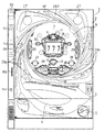
まず、遊技機の一例であるパチンコ遊技機の全体の構成について説明する。図1はパチンコ遊技機を正面からみた正面図、図2は遊技盤の前面を示す正面図である。なお、以下の実施の形態では、パチンコ遊技機を例に説明を行うが、本発明による遊技機はパチンコ遊技機に限られず、例えば画像式の遊技機やスロット機に適用することもできる。
【0025】
パチンコ遊技機1は、縦長の方形状に形成された外枠(図示せず)と、外枠の内側に開閉可能に取り付けられた遊技枠とで構成される。また、パチンコ遊技機1は、遊技枠に開閉可能に設けられている額縁状に形成されたガラス扉枠2を有する。遊技枠は、外枠に対して開閉自在に設置される前面枠(図示せず)と、機構部品等が取り付けられる機構板と、それらに取り付けられる種々の部品(後述する遊技盤を除く。)とを含む構造体である。
【0026】
図1に示すように、パチンコ遊技機1は、額縁状に形成されたガラス扉枠2を有する。ガラス扉枠2の下部表面には打球供給皿(上皿)3がある。打球供給皿3の下部には、打球供給皿3に収容しきれない遊技球を貯留する余剰球受皿4と打球を発射する打球操作ハンドル(操作ノブ)5が設けられている。ガラス扉枠2の背面には、遊技盤6が着脱可能に取り付けられている。なお、遊技盤6は、それを構成する板状体と、その板状体に取り付けられた種々の部品とを含む構造体である。また、遊技盤6の前面には遊技領域7が形成されている。
【0027】
遊技領域7の中央付近には、それぞれが識別情報としての図柄を可変表示する複数の可変表示部を含む可変表示装置(特別図柄表示装置)9が設けられている。可変表示装置9には、例えば「左」、「中」、「右」の3つの可変表示部(図柄表示エリア)がある。可変表示装置9の下方には、始動入賞口14が設けられている。始動入賞口14に入った入賞球は、遊技盤6の背面に導かれ、始動口スイッチ14aによって検出される。また、始動入賞口14の下部には開閉動作を行う可変入賞球装置15が設けられている。可変入賞球装置15は、ソレノイド16によって開状態とされる。
【0028】
可変入賞球装置15の下部には、特定遊技状態(大当り状態)においてソレノイド21によって開状態とされる開閉板20が設けられている。開閉板20は大入賞口を開閉する手段である。開閉板20から遊技盤6の背面に導かれた入賞球のうち一方(V入賞領域)に入った入賞球はV入賞スイッチ22で検出され、開閉板20からの入賞球はカウントスイッチ23で検出される。遊技盤6の背面には、大入賞口内の経路を切り換えるためのソレノイド21Aも設けられている。また、可変表示装置9の下部には、始動入賞口14に入った有効入賞球数すなわち始動記憶数を表示する4つのLEDによる特別図柄始動記憶表示器(以下、始動記憶表示器という。)18が設けられている。有効始動入賞がある毎に、始動記憶表示器18は点灯するLEDを1増やす。そして、可変表示装置9の可変表示が開始される毎に、点灯するLEDを1減らす。
【0029】
ゲート32に遊技球が入賞しゲートスイッチ32aで検出されると、普通図柄表示器10の表示の可変表示が開始される。この実施の形態では、左右のランプ(点灯時に図柄が視認可能になる)が交互に点灯することによって可変表示が行われ、例えば、可変表示の終了時に右側のランプが点灯すれば当たりとなる。そして、普通図柄表示器10における停止図柄が所定の図柄(当り図柄)である場合に、可変入賞球装置15が所定回数、所定時間だけ開状態になる。普通図柄表示器10の近傍には、ゲート32に入った入賞球数を表示する4つのLEDによる表示部を有する普通図柄始動記憶表示器41が設けられている。ゲート32への入賞がある毎に、普通図柄始動記憶表示器41は点灯するLEDを1増やす。そして、普通図柄表示器10の可変表示が開始される毎に、点灯するLEDを1減らす。
【0030】
遊技盤6には、複数の入賞口29,30,33,39が設けられ、遊技球の入賞口29,30,33への入賞は、それぞれ入賞口スイッチ29a,30a,33a,39aによって検出される。各入賞口29,30,33,39は、遊技媒体を受け入れて入賞を許容する領域として遊技盤6に設けられる入賞領域を構成している。なお、遊技媒体を受け入れて入賞を許容する始動入賞口14や、大入賞口も、入賞領域を構成する。遊技領域7の左右周辺には、遊技中に点滅表示される装飾ランプ25が設けられ、下部には、入賞しなかった打球を吸収するアウト口26がある。また、遊技領域7の外側の左右上部には、効果音を発する2つのスピーカ27が設けられている。遊技領域7の外周には、天枠ランプ28a、左枠ランプ28bおよび右枠ランプ28cが設けられている。さらに、遊技領域7における各構造物(大入賞口等)の周囲には装飾LEDが設置されている。天枠ランプ28a、左枠ランプ28bおよび右枠ランプ28cおよび装飾用LEDは、遊技機に設けられている装飾発光体の一例である。
【0031】
そして、この例では、左枠ランプ28bの近傍に、賞球残数があるときに点灯する賞球ランプ51が設けられ、天枠ランプ28aの近傍に、補給球が切れたときに点灯する球切れランプ52が設けられている。上記のように、本例のパチンコ遊技機1には、発光体としてのランプやLEDが各所に設けられている。さらに、図1には、パチンコ遊技機1に隣接して設置され、プリペイドカードが挿入されることによって球貸しを可能にするカードユニット(プリペイドカードユニット)50も示されている。
【0032】
カードユニット50には、使用可能状態であるか否かを示す使用可表示ランプ151、カードユニット50がいずれの側のパチンコ遊技機1に対応しているのかを示す連結台方向表示器153、カードユニット50内にカードが投入されていることを示すカード投入表示ランプ154、記録媒体としてのカードが挿入されるカード挿入口155、およびカード挿入口155の裏面に設けられているカードリーダライタの機構を点検する場合にカードユニット50を解放するためのカードユニット錠156が設けられている。
【0033】
打球発射装置から発射された遊技球は、打球レールを通って遊技領域7に入り、その後、遊技領域7を下りてくる。打球が始動入賞口14に入り始動口スイッチ14aで検出されると、図柄の可変表示を開始できる状態であれば、可変表示装置9において特別図柄が可変表示(変動)を始める。図柄の可変表示を開始できる状態でなければ、始動記憶数を1増やす。
【0034】
可変表示装置9における特別図柄の可変表示は、一定時間が経過したときに停止する。停止時の特別図柄の組み合わせが大当り図柄(特定表示結果)であると、大当り遊技状態に移行する。すなわち、開閉板20が、一定時間経過するまで、または、所定個数(例えば10個)の打球が入賞するまで開放する。そして、開閉板20の開放中に打球がV入賞領域に入賞しV入賞スイッチ22で検出されると、継続権が発生し開閉板20の開放が再度行われる。継続権の発生は、所定回数(例えば15ラウンド)許容される。
【0035】
停止時の可変表示装置9における特別図柄の組み合わせが確率変動を伴う大当り図柄(確変図柄)の組み合わせである場合には、次に大当りとなる確率が高くなる。すなわち、確変状態という遊技者にとってさらに有利な状態となる。
【0036】
打球がゲート32に入賞すると、普通図柄表示器10において普通図柄が可変表示される状態になる。また、普通図柄表示器10における停止図柄が所定の図柄(当り図柄)である場合に、可変入賞球装置15が所定時間だけ開状態になる。さらに、確変状態では、普通図柄表示器10における停止図柄が当り図柄になる確率が高められるとともに、可変入賞球装置15の開放時間と開放回数が高められる。すなわち、可変入賞球装置15の開放時間と開放回数は、普通図柄の停止図柄が当り図柄であったり、特別図柄の停止図柄が確変図柄である場合等に高められ、遊技者にとって不利な状態から有利な状態に変化する。なお、開放回数が高められることは、閉状態から開状態になることも含む概念である。
【0037】
次に、パチンコ遊技機1の裏面の構造について図3および図4を参照して説明する。図3は、遊技機を裏面から見た背面図である。図4は、各種部材が取り付けられた機構板を遊技機背面側から見た背面図である。
【0038】
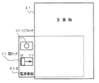
図3に示すように、遊技機裏面側では、可変表示装置9を制御する図柄制御基板80を含む可変表示制御ユニット49、遊技制御用マイクロコンピュータ等が搭載された遊技制御基板(主基板)31が設置されている。また、球払出制御を行う払出制御用マイクロコンピュータ等が搭載された払出制御基板37が設置されている。さらに、遊技盤6に設けられている各種装飾LED、始動記憶表示器18および普通図柄始動記憶表示器41、装飾ランプ25、枠側に設けられている天枠ランプ28a、左枠ランプ28b、右枠ランプ28c、賞球ランプ51および球切れランプ52を点灯制御するランプ制御手段が搭載されたランプ制御基板35、スピーカ27からの音発生を制御する音制御手段が搭載された音制御基板70も設けられている。また、また、DC30V、DC21V、DC12VおよびDC5Vを作成する電源回路が搭載された電源基板910や発射制御基板91が設けられている。
【0039】
遊技機裏面において、上方には、各種情報を遊技機外部に出力するための各端子を備えたターミナル基板160が設置されている。ターミナル基板160には、少なくとも、球切れ検出スイッチの出力を導入して外部出力するための球切れ用端子、賞球個数信号を外部出力するための賞球用端子および球貸し個数信号を外部出力するための球貸し用端子が設けられている。また、中央付近には、主基板31からの各種情報を遊技機外部に出力するための各端子を備えた情報端子基板(情報出力基板)34が設置されている。
【0040】
貯留タンク38に貯留された遊技球は誘導レール39を通り、図4に示されるように、カーブ樋186を経て賞球ケース40Aで覆われた球払出装置に至る。球払出装置の上部には、遊技媒体切れ検出手段としての球切れスイッチ187が設けられている。球切れスイッチ187が球切れを検出すると、球払出装置の払出動作が停止する。球切れスイッチ187は遊技球通路内の遊技球の有無を検出するスイッチであるが、貯留タンク38内の補給球の不足を検出する球切れ検出スイッチ167も誘導レール39における上流部分(貯留タンク38に近接する部分)に設けられている。球切れ検出スイッチ167が遊技球の不足を検知すると、遊技機設置島に設けられている補給機構から遊技機に対して遊技球の補給が行われる。
【0041】
入賞にもとづく景品としての遊技球や球貸し要求にもとづく遊技球が多数払い出されて打球供給皿3が満杯になり、ついには遊技球が連絡口45に到達した後さらに遊技球が払い出されると、遊技球は、余剰球通路46を経て余剰球受皿4に導かれる。さらに遊技球が払い出されると、感知レバー47が貯留状態検出手段としての満タンスイッチ48を押圧して、貯留状態検出手段としての満タンスイッチ48がオンする。その状態では、球払出装置内の払出モータの回転が停止して球払出装置の動作が停止するとともに発射装置の駆動も停止する。
【0042】
図4に示すように、球払出装置の側方には、カーブ樋186から遊技機下部の排出口192に至る球抜き通路191が形成されている。球抜き通路191の上部には球抜きレバー193が設けられ、球抜きレバー193が遊技店員等によって操作されると、誘導レール39から球抜き通路191への遊技球通路が形成され、貯留タンク38内に貯留されている遊技球は、排出口192から遊技機外に排出される。
【0043】
図5は、球払出装置97の構成例を示す分解斜視図である。この例では、賞球ケース40Aとしての3つのケース140,141,142の内部に球払出装置97が形成されている。ケース140,141の上部には、球切れスイッチ187の下部の球通路と連通する穴170,171が設けられ、遊技球は、穴170,171から球払出装置97に流入する。
【0044】
球払出装置97は駆動源となる払出モータ(例えばステッピングモータ)289を含む。払出モータ289の回転力は、払出モータ289の回転軸に嵌合しているギア290に伝えられ、さらに、ギア290と噛み合うギア291に伝えられる。ギア291の中心軸には、凹部を有するスプロケット292が嵌合している。穴170,171から流入した遊技球は、スプロケット292の凹部によって、スプロケット292の下方の球通路293a,293bに1個ずつ落下させられる。
【0045】
球通路(遊技媒体払出通路の一例)293a,293bには遊技球の流下路を切り替えるための振分部材311が設けられている。振分部材311はソレノイド310によって駆動され、賞球払出時には、球通路293a,293bにおける一方の流下路(球通路293a:景品遊技媒体通路の一例)を遊技球が流下するように倒れ、球貸し時には球通路293a,293bにおける他方の流下路(球通路293b:貸出遊技媒体通路の一例)を遊技球が流下するように倒れる。なお、払出モータ289およびソレノイド310は、払出制御基板37に搭載されている払出制御用CPUによって制御される。また、払出制御用CPUは、主基板31に搭載されている遊技制御用のCPUからの指令に応じて払出モータ289およびソレノイド310を制御する。
【0046】
賞球払出時に選択される流下路の下方には球払出装置によって払い出された遊技球を検出する賞球センサ(賞球カウントスイッチ)301Aが設けられ、球貸し時に選択される流下路の下方には球払出装置によって払い出された遊技球を検出する球貸しセンサ(球貸しカウントスイッチ)301Bが設けられている。賞球カウントスイッチ301Aの検出信号と球貸しカウントスイッチ301Bの検出信号は払出制御基板37の払出制御用CPUに入力される。払出制御用CPUは、それらの検出信号にもとづいて、実際に払い出された遊技球の個数を計数する。なお、賞球カウントスイッチ301Aの検出信号は、主基板31のCPUにも入力される。球貸しカウントスイッチ301Bに対する電源基板910からの電力供給は、払出制御基板37を介してなされる。なお、賞球カウントスイッチ301Aに対する電源基板910からの電力供給は、主基板31を介してなされるが、払出制御基板37を介してなされるようにしてもよい。また、賞球センサと球貸しセンサは、それぞれ複数設けられていてもよい。また、賞球センサは、主基板31用のものと払出制御基板37用のものが別個に設けられていてもよい。
【0047】
なお、ギア291の周辺部には、払出モータ位置センサを形成する突起部が形成されている。突起部は、ギア291の回転すなわち払出モータ289の回転に伴って発光体(図示せず)からの光を、払出モータ位置センサの受光部(図示せず)に対して透過させたり遮蔽したりする。払出制御用CPUは、受光部からの検出信号によって払出モータ289の位置を認識することができる。
【0048】
また、球払出装置は、賞球払出と球貸しとを共に行うように構成されていてもよいが、賞球払出を行う球払出装置と球貸しを行う球払出装置が別個に設けられていてもよい。さらに、例えばスプロケットの回転方向を変えて賞球払出と球貸しとを分けるように構成されていてもよいし、本実施の形態において例示する球払出装置97以外のどのような構造の球払出装置を用いても、本発明を適用することができる。
【0049】
図6は、遊技枠を構成する機構板に設置されている電源基板910の露出部分を示す正面図である。図6に示すように、電源基板910は、大部分が主基板31と重なっているが、主基板31に重なることなく外部から視認可能に露出した露出部分がある。この露出部分には、遊技機1への電力供給を実行あるいは遮断するための電源スイッチ914と、各基板(主基板31や払出制御基板37等)に含まれる記憶内容保持手段(例えば、電力供給停止時にもその内容を保持可能なバックアップRAM)に記憶されたバックアップデータをクリアするための操作手段としてのクリアスイッチ921とが設けられている。このように、電源スイッチ914とクリアスイッチ921とが近くに配置されているので、クリアスイッチ921の操作が容易となる。
【0050】
図7は、主基板31における回路構成の一例を示すブロック図である。なお、図7には、払出制御基板37、ランプ制御基板35、音制御基板70、発射制御基板91および図柄制御基板80も示されている。主基板31には、プログラムに従ってパチンコ遊技機1を制御する基本回路53と、ゲートスイッチ32a、始動口スイッチ14a、V入賞スイッチ22、カウントスイッチ23、入賞口スイッチ29a,30a,33a,39a、満タンスイッチ48、球切れスイッチ187、賞球カウントスイッチ301Aおよびクリアスイッチ921からの信号を基本回路53に与えるスイッチ回路58と、可変入賞球装置15を開閉するソレノイド16、開閉板20を開閉するソレノイド21および大入賞口内の経路を切り換えるためのソレノイド21Aを基本回路53からの指令に従って駆動するソレノイド回路59とが搭載されている。
【0051】
なお、図7には示されていないが、カウントスイッチ短絡信号もスイッチ回路58を介して基本回路53に伝達される。また、ゲートスイッチ32a、始動口スイッチ14a、V入賞スイッチ22、カウントスイッチ23、入賞口スイッチ29a,30a,33a,39a、満タンスイッチ48、球切れスイッチ187、賞球カウントスイッチ301A等のスイッチは、センサと称されているものでもよい。すなわち、遊技球を検出できる遊技媒体検出手段(この例では遊技球検出手段)であれば、その名称を問わない。特に、入賞検出を行う始動口スイッチ14a、カウントスイッチ23、および入賞口スイッチ29a,30a,33a,39aの各スイッチは、入賞検出手段でもある。なお、入賞検出手段は、複数の入賞口に別個に入賞したそれぞれの遊技球をまとめて検出するものであってもよい。また、ゲートスイッチ32aのような通過ゲートであっても、賞球の払い出しが行われるものであれば、通過ゲートへ遊技球が進入することが入賞となり、通過ゲートに設けられているスイッチ(例えばゲートスイッチ32a)が入賞検出手段となる。
【0052】
また、基本回路53から与えられるデータに従って、大当りの発生を示す大当り情報、可変表示装置9における図柄の可変表示開始に利用された始動入賞球の個数を示す有効始動情報、確率変動が生じたことを示す確変情報等の情報出力信号をホールコンピュータ等の外部装置に対して出力する情報出力回路64が搭載されている。
【0053】
基本回路53は、ゲーム制御用のプログラム等を記憶するROM54、ワークメモリとして使用される記憶手段(変動データを記憶する手段)としてのRAM55、プログラムに従って制御動作を行うCPU56およびI/Oポート部57を含む。この実施の形態では、ROM54,RAM55はCPU56に内蔵されている。すなわち、CPU56は、1チップマイクロコンピュータである。なお、1チップマイクロコンピュータは、少なくともRAM55が内蔵されていればよく、ROM54およびI/Oポート部57は外付けであっても内蔵されていてもよい。
【0054】
また、RAM(CPU内蔵RAMであってもよい。)55の一部または全部が、電源基板910において作成されるバックアップ電源よってバックアップされているバックアップRAMである。すなわち、遊技機に対する電力供給が停止しても、所定期間は、RAM55の一部または全部の内容は保存される。
【0055】
この実施の形態では、電源基板910から主基板31に対して、ローレベルがリセット状態を示すリセット信号、ローアクティブの復帰信号およびローアクティブの電源断信号も入力される。リセット信号と復帰信号とはAND回路161に入力され、AND回路161の出力がCPU56のリセット端子に入力される。また、電源断信号は、CPU56のマスク不能割込(NMI)端子に入力される。
【0056】
遊技球を打撃して発射する打球発射装置は発射制御基板91上の回路によって制御される駆動モータ94で駆動される。そして、駆動モータ94の駆動力は、操作ノブ5の操作量に従って調整される。すなわち、発射制御基板91上の回路によって、操作ノブ5の操作量に応じた速度で打球が発射されるように制御される。
【0057】
なお、この実施の形態では、ランプ制御基板35に搭載されているランプ制御手段が、遊技盤に設けられている始動記憶表示器18、普通図柄始動記憶表示器41および装飾ランプ25の表示制御を行うとともに、枠側に設けられている天枠ランプ28a、左枠ランプ28b、右枠ランプ28c、賞球ランプ51および球切れランプ52の表示制御を行う。また、特別図柄を可変表示する可変表示装置9および普通図柄を可変表示する普通図柄表示器10の表示制御は、図柄制御基板80に搭載されている表示制御手段によって行われる。
【0058】
図8は、払出制御基板37および球払出装置97の構成要素などの払出に関連する構成要素を示すブロック図である。図8に示すように、満タンスイッチ48からの検出信号は、中継基板71を介して主基板31のI/Oポート部57に入力される。また、球切れスイッチ187からの検出信号も、中継基板72および中継基板71を介して主基板31のI/Oポート部57に入力される。
【0059】
主基板31のCPU56は、球切れスイッチ187からの検出信号が球切れ状態を示しているか、または、満タンスイッチ48からの検出信号が満タン状態を示していると、払出を停止すべき状態であることを指示する払出制御コマンドを送出する。払出を停止すべき状態であることを指示する払出制御コマンドを受信すると、払出制御基板37の払出制御用CPU371は球払出処理を停止する。
【0060】
さらに、賞球カウントスイッチ301Aからの検出信号は、中継基板72および中継基板71を介して主基板31のI/Oポート部57に入力されるとともに、中継基板72を介して払出制御基板37の入力ポート372bに入力される。賞球カウントスイッチ301Aは、球払出装置97の払出機構部分に設けられ、実際に払い出された賞球払出球を検出する。
【0061】
入賞があると、払出制御基板37には、主基板31の出力ポート(ポート0,1)570,571から賞球個数を示す払出制御コマンドが入力される。出力ポート(出力ポート1)571は8ビットのデータを出力し、出力ポート(出力ポート0)570は1ビットのINT信号を出力する。賞球個数を示す払出制御コマンドは、入力バッファ回路373Aを介してI/Oポート372aに入力される。INT信号は、入力バッファ回路373Bを介して払出制御用CPU371の割込端子に入力されている。払出制御用CPU371は、I/Oポート372aを介して払出制御コマンドを入力し、払出制御コマンドに応じて球払出装置97を駆動して賞球払出を行う。なお、この実施の形態では、払出制御用CPU371は、1チップマイクロコンピュータであり、少なくともRAMが内蔵されている。
【0062】
また、主基板31において、出力ポート570,571の外側にバッファ回路620,68Aが設けられている。バッファ回路620,68Aとして、例えば、汎用のCMOS−ICである74HC250,74HC14が用いられる。このような構成によれば、外部から主基板31の内部に入力される信号が阻止されるので、払出制御基板37から主基板31に信号が与えられる可能性がある信号ラインをさらに確実になくすことができる。なお、バッファ回路620,68Aの出力側にノイズフィルタを設けてもよい。
【0063】
払出制御用CPU371は、出力ポート372cを介して、貸し球数を示す球貸し個数信号をターミナル基板160に出力する。さらに、出力ポート372dを介して、エラー表示用LED374にエラー信号を出力する。
【0064】
さらに、払出制御基板37の入力ポート372bには、中継基板72を介して、球貸しカウントスイッチ301B、および払出モータ289の回転位置を検出するための払出モータ位置センサからの検出信号が入力される。球貸しカウントスイッチ301Bは、球払出装置97の払出機構部分に設けられ、実際に払い出された貸し球を検出する。払出制御基板37からの払出モータ289への駆動信号は、出力ポート372cおよび中継基板72を介して球払出装置97の払出機構部分における払出モータ289に伝えられ、振分ソレノイド310への駆動信号は、出力ポート372eおよび中継基板72を介して球払出装置97の払出機構部分における振分ソレノイド310に伝えられる。また、クリアスイッチ921の出力も、入力ポート372bに入力される。
【0065】
カードユニット50には、カードユニット制御用マイクロコンピュータが搭載されている。また、カードユニット50には、使用可表示ランプ151、連結台方向表示器153、カード投入表示ランプ154およびカード挿入口155が設けられている(図1参照)。残高表示基板74には、打球供給皿3の近傍に設けられている度数表示LED、球貸しスイッチおよび返却スイッチが接続される。
【0066】
残高表示基板74からカードユニット50には、遊技者の操作に応じて、球貸しスイッチ信号および返却スイッチ信号が払出制御基板37を介して与えられる。また、カードユニット50から残高表示基板74には、プリペイドカードの残高を示すカード残高表示信号および球貸し可表示信号が払出制御基板37を介して与えられる。このように、残高表示基板74とカードユニット50は、直接接続されることなく、払出制御基板37を介して接続されている。カードユニット50と払出制御基板37の間では、接続信号(VL信号)、ユニット操作信号(BRDY信号)、球貸し要求信号(BRQ信号)、球貸し完了信号(EXS信号)およびパチンコ機動作信号(PRDY信号)が入力ポート372bおよび出力ポート372eを介してやりとりされる。なお、カードユニット50と払出制御基板37の間には、図示しないインタフェース基板が介在しており、接続信号(VL信号)等の信号はインタフェース基板を介してやりとりされる。
【0067】
パチンコ遊技機1の電源が投入されると、払出制御基板37の払出制御用CPU371は、カードユニット50にPRDY信号を出力する。また、カードユニット制御用マイクロコンピュータは、VL信号を出力する。払出制御用CPU371は、VL信号の入力状態により接続状態/未接続状態を判定する。カードユニット50においてカードが受け付けられ、球貸しスイッチが操作され球貸しスイッチ信号が入力されると、カードユニット制御用マイクロコンピュータは、払出制御基板37にBRDY信号を出力する。この時点から所定の遅延時間が経過すると、カードユニット制御用マイクロコンピュータは、払出制御基板37にBRQ信号を出力する。
【0068】
そして、払出制御基板37の払出制御用CPU371は、カードユニット50に対するEXS信号を立ち上げ、カードユニット50からのBRQ信号の立ち下がりを検出すると、払出モータ289を駆動し、所定個の貸し球を遊技者に払い出す。このとき、振分ソレノイド310は駆動状態とされている。すなわち、球振分部材311を球貸し側に向ける。そして、払出が完了したら、払出制御用CPU371は、カードユニット50に対するEXS信号を立ち下げる。その後、カードユニット50からのBRDY信号がオン状態でなければ、賞球払出制御を実行する。
【0069】
以上のように、カードユニット50からの信号は全て払出制御基板37に入力される構成になっている。従って、球貸し制御に関して、カードユニット50から主基板31に信号が入力されることはなく、主基板31の基本回路53にカードユニット50の側から不正に信号が入力される余地はない。また、カードユニット50で用いられる電源電圧AC24Vは払出制御基板37から供給される。
【0070】
この実施の形態では、電源基板910から払出制御基板37に対して、リセット信号、復帰信号および電源断信号も入力される。リセット信号と復帰信号とはAND回路385に入力され、AND回路385の出力が払出制御用CPU371のリセット端子に入力される。また、電源断信号は、払出制御用CPU371のマスク不能割込(NMI)端子に入力される。さらに、払出制御基板37に存在するRAM(CPU内蔵RAMであってもよい。)の少なくとも一部は、電源基板910において作成されるバックアップ電源によって、バックアップされている。すなわち、遊技機に対する電力供給が停止しても、所定期間は、RAMの少なくとも一部の内容は保存される。
【0071】
なお、この実施の形態では、カードユニット50が遊技機とは別体として遊技機に隣接して設置されている場合を例にするが、カードユニット50は遊技機と一体化されていてもよい。また、コイン投入に応じてその金額に応じた遊技球が貸し出されるような場合でも本発明を適用できる。
【0072】
図9は、図柄制御基板80内の回路構成を、可変表示装置9の一実現例であるLCD(液晶表示装置)82、普通図柄表示器10、主基板31の出力ポート(ポート0,2)570,572および出力バッファ回路620,62Aとともに示すブロック図である。出力ポート(出力ポート2)572からは8ビットのデータが出力され、出力ポート570からは1ビットのストローブ信号(INT信号)が出力される。
【0073】
表示制御用CPU101は、制御データROM102に格納されたプログラムに従って動作し、主基板31からノイズフィルタ107および入力バッファ回路105Bを介してINT信号が入力されると、入力バッファ回路105Aを介して表示制御コマンドを受信する。入力バッファ回路105A,105Bとして、例えば汎用ICである74HC540,74HC14を使用することができる。なお、表示制御用CPU101がI/Oポートを内蔵していない場合には、入力バッファ回路105A,105Bと表示制御用CPU101との間に、I/Oポートが設けられる。
【0074】
そして、表示制御用CPU101は、受信した表示制御コマンドに従って、LCD82に表示される画面の表示制御を行う。具体的には、表示制御コマンドに応じた指令をVDP(ビデオディスプレイプロセッサ)103に与える。VDP103は、キャラクタROM86から必要なデータを読み出す。VDP103は、入力したデータに従ってLCD82に表示するための画像データを生成し、R,G,B信号および同期信号をLCD82に出力する。
【0075】
なお、図9には、VDP103をリセットするためのリセット回路83、VDP103に動作クロックを与えるための発振回路85、および使用頻度の高い画像データを格納するキャラクタROM86も示されている。キャラクタROM86に格納される使用頻度の高い画像データとは、例えば、LCD82に表示される人物、動物、または、文字、図形もしくは記号等からなる画像などである。
【0076】
入力バッファ回路105A,105Bは、主基板31から図柄制御基板80へ向かう方向にのみ信号を通過させることができる。従って、図柄制御基板80側から主基板31側に信号が伝わる余地はない。すなわち、入力バッファ回路105A,105Bは、入力ポートともに不可逆性情報入力手段を構成する。図柄制御基板80内の回路に不正改造が加えられても、不正改造によって出力される信号が主基板31側に伝わることはない。
【0077】
高周波信号を遮断するノイズフィルタ107として、例えば3端子コンデンサやフェライトビーズが使用されるが、ノイズフィルタ107の存在によって、表示制御コマンドに基板間でノイズが乗ったとしても、その影響は除去される。また、主基板31のバッファ回路620,62Aの出力側にもノイズフィルタを設けてもよい。
【0078】
図10は、主基板31およびランプ制御基板35における信号送受信部分を示すブロック図である。この実施の形態では、遊技領域7の外側に設けられている点枠ランプ28a、左枠ランプ28b、右枠ランプ28cと遊技盤に設けられている装飾ランプ25の点灯/消灯と、賞球ランプ51および球切れランプ52の点灯/消灯とを示すランプ制御コマンドが主基板31からランプ制御基板35に出力される。また、始動記憶表示器18および普通図柄始動記憶表示器41の点灯個数を示すランプ制御コマンドも主基板31からランプ制御基板35に出力される。
【0079】
図10に示すように、ランプ制御に関するランプ制御コマンドは、基本回路53におけるI/Oポート部57の出力ポート(出力ポート0,3)570,573から出力される。出力ポート(出力ポート3)573は8ビットのデータを出力し、出力ポート570は1ビットのINT信号を出力する。ランプ制御基板35において、主基板31からの制御コマンドは、入力バッファ回路355A,355Bを介してランプ制御用CPU351に入力する。なお、ランプ制御用CPU351がI/Oポートを内蔵していない場合には、入力バッファ回路355A,355Bとランプ制御用CPU351との間に、I/Oポートが設けられる。
【0080】
ランプ制御基板35において、ランプ制御用CPU351は、各制御コマンドに応じて定義されている天枠ランプ28a、左枠ランプ28b、右枠ランプ28c、装飾ランプ25の点灯/消灯パターンに従って、天枠ランプ28a、左枠ランプ28b、右枠ランプ28c、装飾ランプ25に対して点灯/消灯信号を出力する。点灯/消灯信号は、天枠ランプ28a、左枠ランプ28b、右枠ランプ28c、装飾ランプ25に出力される。なお、点灯/消灯パターンは、ランプ制御用CPU351の内蔵ROMまたは外付けROMに記憶されている。
【0081】
主基板31において、CPU56は、RAM55の記憶内容に未払出の賞球残数があるときに賞球ランプ51の点灯を指示する制御コマンドを出力し、遊技盤裏面の払出球通路の上流に設置されている球切れスイッチ187(図3参照)が遊技球を検出しなくなると球切れランプ52の点灯を指示する制御コマンドを出力する。ランプ制御基板35において、各制御コマンドは、入力バッファ回路355A,355Bを介してランプ制御用CPU351に入力する。ランプ制御用CPU351は、それらの制御コマンドに応じて、賞球ランプ51および球切れランプ52を点灯/消灯する。なお、点灯/消灯パターンは、ランプ制御用CPU351の内蔵ROMまたは外付けROMに記憶されている。
【0082】
さらに、ランプ制御用CPU351は、制御コマンドに応じて始動記憶表示器18および普通図柄始動記憶表示器41に対して点灯/消灯信号を出力する。
【0083】
入力バッファ回路355A,355Bとして、例えば、汎用のCMOS−ICである74HC540,74HC14が用いられる。入力バッファ回路355A,355Bは、主基板31からランプ制御基板35へ向かう方向にのみ信号を通過させることができる。従って、ランプ制御基板35側から主基板31側に信号が伝わる余地はない。たとえ、ランプ制御基板35内の回路に不正改造が加えられても、不正改造によって出力される信号がメイン基板31側に伝わることはない。なお、入力バッファ回路355A,355Bの入力側にノイズフィルタを設けてもよい。
【0084】
また、主基板31において、出力ポート570,573の外側にバッファ回路620,63Aが設けられている。バッファ回路620,63Aとして、例えば、汎用のCMOS−ICである74HC250,74HC14が用いられる。このような構成によれば、外部から主基板31の内部に入力される信号が阻止されるので、ランプ制御基板35から主基板31に信号が与えられる可能性がある信号ラインをさらに確実になくすことができる。なお、バッファ回路620,63Aの出力側にノイズフィルタを設けてもよい。
【0085】
図11は、電源基板910の一構成例を示すブロック図である。電源基板910は、主基板31、図柄制御基板80、音制御基板70、ランプ制御基板35および払出制御基板37等の電気部品制御基板と独立して設置され、遊技機内の各電気部品制御基板および機構部品が使用する電圧を生成する。この例では、AC24V、VSL(DC+30V)、DC+21V、DC+12VおよびDC+5Vを生成する。また、バックアップ電源すなわち記憶保持手段となるコンデンサ916は、DC+5Vすなわち各基板上のIC等を駆動する電源のラインから充電される。なお、VSLは、整流回路912において、整流素子でAC24Vを整流昇圧することによって生成される。VSLは、ソレノイド駆動電源となる。
【0086】
電源基板910には、遊技機内の各電気部品制御基板や機構部品への電力供給を実行または遮断するための電源スイッチ914が設けられている。トランス911は、交流電源からの交流電圧を24Vに変換する。AC24V電圧は、コネクタ915に出力される。また、整流回路912は、AC24Vから+30Vの直流電圧を生成し、DC−DCコンバータ913およびコネクタ915に出力する。DC−DCコンバータ913は、1つまたは複数のコンバータIC920(図11では1つのみを示す。)を有し、VSLにもとづいて+21V、+12Vおよび+5Vを生成してコネクタ915に出力する。コンバータIC920の入力側には、比較的大容量のコンデンサ923が接続されている。従って、外部からの遊技機に対する電力供給が停止したときに、+30V、+12V、+5V等の直流電圧は、比較的緩やかに低下する。また、コネクタ915の入力側にも、比較的大容量のコンデンサ924が接続されている。従って、コネクタ915に出力される+30Vの直流電圧は、他の直流電圧よりもさらに緩やかに低下する。この結果、コンデンサ923,924は、後述する補助駆動電源の役割を果たす。コネクタ915は例えば中継基板に接続され、中継基板から各電気部品制御基板および機構部品に必要な電圧の電力が供給される。
【0087】
ただし、電源基板910に各電気部品制御基板に至る各コネクタを設け、電源基板910から、中継基板を介さずにそれぞれの基板に至る各電圧を供給するようにしてもよい。また、図11には1つのコネクタ915が代表して示されているが、コネクタは、各電気部品制御基板対応に設けられている。
【0088】
DC−DCコンバータ913からの+5Vラインは分岐してバックアップ+5Vラインを形成する。バックアップ+5Vラインとグラウンドレベルとの間には大容量のコンデンサ916が接続されている。コンデンサ916は、遊技機に対する電力供給が停止したときの電気部品制御基板のバックアップRAM(電源バックアップされているRAMすなわち電力供給停止時にも記憶内容保持状態となりうるバックアップ記憶手段)に対して記憶状態を保持できるように電力を供給するバックアップ電源となる。また、+5Vラインとバックアップ+5Vラインとの間に、逆流防止用のダイオード917が挿入される。なお、この実施の形態では、バックアップ用の+5Vは、主基板31および払出制御基板37に供給される。
【0089】
なお、バックアップ電源として、+5V電源から充電可能な電池を用いてもよい。電池を用いる場合には、+5V電源から電力供給されない状態が所定時間継続すると容量がなくなるような充電池が用いられる。また、上記のコンデンサ923,924の代わりに、+30V電源から充電可能な電池を用いてもよい。コンデンサ923の代わりに電池を用いる場合には、後述する払出確認期間以上の期間、賞球カウントスイッチ301Aや球貸しカウントスイッチ301Bに電力を供給可能な充電池が用いられる。また、コンデンサ924の代わりに電池を用いる場合には、後述する払出確認期間以上の期間、振分ソレノイド310に電力を供給可能な充電池が用いられる。なお、上記の電池は、充電機能を有するものでなくてもよく、例えばニッカド電池、アルカリ電池、マンガン電池などの電池が用いられる。
【0090】
また、電源基板910には、電源監視回路としての電源監視用IC902が搭載されている。電源監視用IC902は、VSL電圧を導入し、VSL電圧を監視することによって遊技機への電力供給停止の発生を検出する。具体的には、VSL電圧が所定値(この例では+22V)以下になったら、電力供給の停止が生ずるとして電源断信号を出力する。従って、賞球カウントスイッチ301Aによる賞球の検出が有効に行われているときに電源供給停止時処理を開始することができる。従って、電源供給停止時処理を開始したあとしばらくは補助駆動電源にたよることなく賞球の検出が可能となり、補助駆動電源としてのコンデンサ923の容量が少なくて済む。なお、監視対象の電源電圧は、各電気部品制御基板に搭載されている回路素子の電源電圧(この例では+5V)よりも高い電圧であることが好ましい。この例では、交流から直流に変換された直後の電圧であるVSLが用いられている。電源監視用IC902からの電源断信号は、主基板31や払出制御基板37等に供給される。
【0091】
電源監視用IC902が電力供給の停止を検知するための所定値は、通常時の電圧より低いが、各電気部品制御基板上のCPUが暫くの間動作しうる程度の電圧である。また、電源監視用IC902が、CPU等の回路素子を駆動するための電圧(この例では+5V)よりも高く、また、交流から直流に変換された直後の電圧を監視するように構成されているので、CPUが必要とする電圧に対して監視範囲を広げることができる。従って、より精密な監視を行うことができる。
【0092】
さらに、監視電圧としてVSL(+30V)を用いる場合には、遊技機の各種スイッチに供給される電圧が+12Vであることから、電源瞬断時のスイッチオン誤検出の防止も期待できる。すなわち、+30V電源の電圧を監視すると、+30V作成の以降に作られる+12Vが落ち始める以前の段階でそれの低下を検出できる。+12V電源の電圧が低下するとスイッチ出力がオン状態を呈するようになるが、+12Vより早く低下する+30V電源電圧を監視して電力供給の停止を認識すれば、スイッチ出力がオン状態を呈する前に電源復旧待ちの状態に入ってスイッチ出力を検出しない状態となることができる。
【0093】
また、監視電圧としてのVSL(+30V)の電源監視用IC902への入力ラインと異なり、ソレノイドやモータなどに供給される電圧としてのVSL(+30V)のコネクタ915への入力ラインには大容量のコンデンサ924が接続されている。従って、監視電圧としてのVSL(+30V)は、大容量のコンデンサ924が接続されているコネクタ915に出力されるVSL(+30V)より早く低下する。すなわち、監視電圧としてのVSL(+30V)が落ち始めたあとも、所定期間は、ソレノイドやモータなどに供給される電圧としてのVSL(+30V)の供給状態が維持される。その後、ソレノイドやモータなどに供給される電圧としてのVSL(+30V)は、緩やかに低下してく。よって、監視電圧としてのVSL(+30V)が落ち始める場合であっても、所定期間は、ソレノイドやモータなどを駆動可能な状態とすることができる。また、コネクタ915に出力されるVSL(+30V)が落ち始める前に、電力供給の停止を認識することができる。
【0094】
また、電源監視用IC902は、電気部品制御基板とは別個の電源基板910に搭載されているので、電源監視回路から複数の電気部品制御基板に電源断信号を供給することができる。電源断信号を必要とする電気部品制御基板が幾つあっても電源監視手段は1つ設けられていればよいので、各電気部品制御基板における各電気部品制御手段が後述する復旧制御を行っても、遊技機のコストはさほど上昇しない。
【0095】
なお、図11に示された構成では、電源監視用IC902の検出信号(電源断信号)は、バッファ回路918,919を介してそれぞれの電気部品制御基板(例えば主基板31と払出制御基板37)に伝達されるが、例えば、1つの検出信号を中継基板に伝達し、中継基板から各電気部品制御基板に同じ信号を分配する構成でもよい。また、電源断信号を必要とする基板数に応じたバッファ回路を設けてもよい。さらに、主基板31と払出制御基板37とに出力される電源断信号について、電源断信号を出力することになる電源監視回路の監視電圧を異ならせてもよい。
【0096】
図11に示すように、電源基板910には、押しボタン構造のクリアスイッチ921が搭載されている。クリアスイッチ921が押下されるとローレベル(オン状態)のクリアスイッチ信号が出力され、コネクタ915を介して主基板31等に送信される。また、クリアスイッチ921が押下されていなければハイレベル(オフ状態)の信号が出力される。
【0097】
なお、クリアスイッチ921が、押しボタン構造以外の他の構成とされていてもよい。図12は、クリアスイッチ921の他の構成例を示す構成図である。図12に示すクリアスイッチ921は、「OFF」、「ON」および「クリア」の選択切り換えを行うための切換操作部921aを有する。切換操作部921aによって、「OFF」が選択されているときは何らの信号も発生しない。「ON」が選択されているときはハイレベルの信号を出力する。なお、クリアスイッチ921が、遊技機1に対する電源供給のオン/オフ切換のためのスイッチも兼ねていてもよい。その場合、「OFF」が選択されると、遊技機1に対する電源供給が停止された状態(遊技機の電源がオフの状態)になる。「ON」または「クリア」が選択されると、遊技機1に対して電源供給が行われる状態(遊技機の電源がオンの状態)になる。また、「クリア」が選択されているときに、ローレベルのクリアスイッチ信号が出力される。
【0098】
この実施の形態では、クリアスイッチ921が電源基板910に搭載されているので、遊技盤6の入れ替え等の場合に入れ替え後の遊技盤6に対して電源基板910をそのまま使用しても、入れ替え後の遊技盤6において、そのままで遊技状態復旧処理等を実行することができる。すなわち、電源基板910の使い回しを行うことができる。なお、電源基板910ではなく、別の箇所にクリアスイッチ921が搭載される構成としてもよい。別の箇所としては、例えば、クリアスイッチ921が搭載されるスイッチ基板や、クリアスイッチ921と電源スイッチ914とが搭載されるターミナル基板などが考えられる。
【0099】
電源基板910には、各基板にリセット信号および復帰信号を供給するリセット管理回路940が搭載されている。リセット管理回路940は、起動順序制御手段の一実現例である。
【0100】
図13は、リセット管理回路940の構成例を示すブロック図である。リセット管理回路940において、リセット回路65におけるリセットIC651は、電源投入時に、外付けのコンデンサの容量で決まる所定時間だけ出力をローレベルとし、所定時間が経過すると出力をハイレベルにする。すなわち、リセット信号をハイレベルに立ち上げてCPU56を動作可能状態にする。また、リセットIC651は、電源監視用IC902が監視する電源電圧と等しい電源電圧であるVSLの電源電圧を監視して電圧値が所定値(電源監視回路が電源断信号を出力する電源電圧値よりも低い値)以下になると出力をローレベルにする。従って、CPU56および払出制御用CPU371は、電源監視用IC902からの電源断信号に応じて所定の電力供給停止時処理を行った後、システムリセットされる(すなわち、システムの最初の状態に戻される)。
【0101】
図13に示すように、リセットIC651に外付けされているコンデンサには、リセットIC651に監視電圧を導入する電源電圧ラインを分岐させたラインが導入されている。このコンデンサは、電力供給が開始されたときに、リセットIC651に導入される監視電圧がその所定値以上の値となることを遅延させるために設けられている。従って、電源供給が開始されると、リセットIC651に導入される電圧は、電源供給が開始してから所定期間が経過したあとに、リセット信号をハイレベルに立ち上げることとなる所定値に到達することとなる。この所定期間は、コンデンサの容量によって決まり、容量を大きくすると期間を長くすることができる。
【0102】
リセットIC651の出力は、リセット信号回路950における各回路941〜949を介して、バッファ回路961〜964および遅延回路960に供給される。遅延回路960の出力はバッファ回路965に入力する。そして、バッファ回路961〜965が各電気部品制御基板にリセット信号として供給される。従って、リセットIC651の出力がハイレベルになると、各電気部品制御基板におけるCPUが動作可能状態になる。
【0103】
図13に示すように、リセットIC651からのリセット信号は、NAND回路947に入力されるとともに、反転回路(NOT回路)944を介してカウンタIC941のクリア端子に入力される。カウンタIC941は、クリア端子への入力がローレベルになると、発振器943からのクロック信号をカウントする。そして、カウンタIC941のQ5出力がNOT回路945,946を介してNAND回路947に入力される。また、カウンタIC941のQ6出力は、フリップフロップ(FF)942のクロック端子に入力される。フリップフロップ942のD入力はハイレベルに固定され、Q出力は論理和回路(OR回路)949に入力される。OR回路949の他方の入力には、NAND回路947の出力がNOT回路948を介して導入される。そして、OR回路949の出力が、バッファ回路961〜965を介して各CPUに供給されている。このような構成によれば、電源投入時に、各CPUのリセット端子に2回のリセット信号(ローレベル信号)が与えられるので、各CPUは、確実に動作を開始する。
【0104】
そして、例えば、電源監視回路の検出電圧(電源断信号を出力することになる電圧)を+22Vとし、リセット信号をローレベルにするための検出電圧を+9Vとする。そのように構成した場合には、電源監視回路とシステムリセット回路65とが、同一の電源VSLの電圧を監視するので、電圧監視回路が電源断信号を出力するタイミングとシステムリセット回路65がシステムリセット信号を出力するタイミングの差を所望の所定期間に確実に設定することができる。所望の所定期間とは、電源監視回路からの電源断信号に応じて電力供給停止時処理を開始してから電力供給停止時処理が確実に完了するまでの期間である。
【0105】
なお、電源監視回路とシステムリセット回路65とが監視する電源の電圧は異なっていてもよい。また、システムリセット回路65は、第2の電源監視手段に相当する。
【0106】
この例では、電源監視手段が検出信号を出力することになる検出条件は+30V電源電圧が+22Vにまで低下したことであり、リセットIC651がリセットレベルであるローレベルを出力することになる条件は+30V電源電圧が+9Vにまで低下したことになる。ただし、ここで用いられている電圧値は一例であって、他の値を用いてもよい。
【0107】
ただし、監視範囲が狭まるが、電源監視手段およびリセットIC651の監視電圧として+5V電源電圧を用いることも可能である。その場合にも、電源監視回路の検出電圧は、リセットIC651の検出電圧よりも高く設定される。
【0108】
主基板31のCPU56および払出制御基板37の払出制御用CPU371の駆動電源である+5V電源から電力が供給されていない間、RAMの少なくとも一部は、電源基板910から供給されるバックアップ電源によってバックアップされ、遊技機に対する電源が断しても内容は保存される。そして、電源が復旧すると、リセット管理回路940からのリセット信号がハイレベルになるので、CPU56および払出制御用CPU371は、通常の動作状態に復帰する。そのとき、必要なデータがバックアップRAMに保存されているので、停電等からの復旧時に停電発生時の遊技状態に復帰することができる。
【0109】
なお、図13には、電源投入時に各電気部品制御基板のCPUのリセット端子に2回のリセット信号(ローレベル信号)が与えられる構成が示されたが、リセット信号の立ち上がりタイミングが1回しかなくても確実にリセット解除されるCPUを使用する場合には、符号941〜949で示された回路素子は不要である。そのような場合などには、符号941〜949で示された回路素子を設けない構成としてもよい。この場合、リセットIC651の出力がそのままバッファ回路961〜964および遅延回路960に接続される。
【0110】
また、上記の例では、電源基板910にリセット回路65が設けられ、主基板31や払出制御基板37などの各基板にリセット信号や復帰信号を出力するようにしていたが、主基板31や払出制御基板37などの各基板それぞれにリセット回路を設ける構成としてもよい。
【0111】
この実施の形態では、電源投入時に、リセット回路65におけるリセットIC651は、外付けのコンデンサの容量で決まる所定時間だけ各電気部品制御基板のCPUに供給しているリセット信号の立ち上げ遅延させる。すなわち、リセットIC651の外付けのコンデンサの容量を、所定の遅延時間を生成するような値に選定すれば、外付けのコンデンサの容量で決まる所定時間だけ出力がローレベルとなり、所定時間が経過すると出力がハイレベルとなる。
【0112】
従って、電源投入時に、リセット信号がハイレベルに立ち上がるタイミングを遅らせて、電源監視回路からの電源断信号(NMI信号)がハイレベルに立ち上がった後にリセット信号をハイレベルに立ち上げるようにすることができ、リセット状態が解除されたときに電源断信号が出力状態となっていて、電源供給が再開して復旧しているときに電源断処理が実行されてしまうことを防止することができる。
【0113】
また、この実施の形態では、電源基板910から各電気部品制御基板のCPUにリセット信号が供給されるときに、遅延回路960が、主基板31のCPU56に対するリセット信号の立ち上げを遅延させる。従って、電源投入時に、主基板31のCPU56が備えるリセット端子の入力信号は、他の電気部品制御基板のCPUに供給されるリセット信号が立ち上げられるときよりも遅く立ち上げられる。
【0114】
例えば、主基板31のCPU56が他の電気部品制御基板に対して制御コマンドを出力する際に、他の電気部品制御基板におけるCPUは既に立ち上がっているので、制御コマンドは確実に受信側の電気部品制御基板のCPUで受信される。
【0115】
さらに、電源基板910には、待機期間を計測して復帰信号を出力する復帰信号出力手段の一例であるカウンタ971が搭載されている。カウンタ971は、電源断信号がローレベルになってクリアが解けると、発振器943からのクロック信号をカウントする。そして、カウントアップすると、Q出力として、ハイレベルの1パルスを発生する。そのパルス信号は反転回路972で論理反転され、バッファ回路973および遅延回路974に入力する。遅延回路974は、入力信号を所定期間遅延させてバッファ回路975に入力させる。
【0116】
バッファ回路973の出力は、払出制御基板37への復帰信号となる。また、バッファ回路975の出力は、主基板31への復帰信号となる。なお、バッファ回路973,975は、払出制御基板37、主基板31に設けられていてもよい。
【0117】
図14は、主基板31におけるCPU56周りの一構成例を示すブロック図である。図14に示すように、電源基板910の電源監視回路(電源監視手段)からの電源断信号が、CPU56のマスク不能割込端子(XNMI端子)に接続されている。上述したように、電源監視回路は、遊技機が使用する各種直流電源のうちのいずれかの電源の電圧を監視して電源電圧低下を検出する回路である。この実施の形態では、VSLの電源電圧を監視して電圧値が所定値以下になるとローレベルの電源断信号を発生する。VSLは、遊技機における直流電圧のうちで最大のものであり、この例では+30Vである。従って、CPU56は、割込処理によって電源断の発生を確認することができる。
【0118】
また、図14に示すように、電源基板910からのリセット信号と復帰信号とはAND回路161に入力され、AND回路161の出力がCPU56のリセット端子(リセット信号入力部)に入力される。
【0119】
図15は、カウンタ971の作用を説明するためのタイミング図である。図15(A)に示すように、電源電圧が低下し、VSLの電圧値が電源断信号出力レベル(この例では+22V)まで低下すると電源断信号が発生する。具体的には、電源断信号がローレベルになる。すると、後述するように、主基板31のCPU31および払出制御用CPU371は、電力供給停止時処理の実行を開始し、その処理が終了すると、何の制御もしないループ状態(待機状態)に入る。
【0120】
カウンタ971は、電源断信号がローレベルになるとカウントを開始するのであるが、カウントアップ値は、電源断信号がローレベルになってから、VSLの電圧値がVcc生成可能電圧にまで低下する時間以上に設定される。すなわち、少なくとも、電源電圧が、制御動作が不能になる電圧にまで低下する時間以上に設定される。カウンタ971はVccを電源として動作するので、カウントアップ値は、カウンタ971の動作可能期間に相当する値以上に設定される。従って、一般には、カウンタ971がカウントアップして復帰信号が出力される前に、カウンタ971およびその他の回路部品は動作しなくなる。
【0121】
電源の瞬断等が生ずると、図15(B)に示すように、VSLの電圧レベルが短期間低下した後に復旧する。VSLの電圧レベルが電源断信号出力レベル以下になると、電源断信号がローレベルになって、電力供給停止時処理が開始される。そして、CPU56および払出制御用CPU371は電力供給停止時処理終了後にループ状態に入る。何らの制御も行わないと、ループ処理から抜けられないのであるが、この場合には、カウンタ971がカウントアップして復帰信号が発生する。
【0122】
図7および図8に示されたように、主基板31および払出制御基板371において、復帰信号は、AND回路161,385を介して、CPU56および払出制御用CPU371のリセット端子に入力される。従って、CPU56および払出制御用CPU371にはシステムリセットがかかる。その結果、CPU56および払出制御用CPU371はループ状態から抜け出すことができる。
【0123】
なお、図15(B)には、カウンタ971のカウントアップ後に、直ちに復帰信号が出力される場合が示されているが、図13に示されたように電源基板910には遅延回路974があるので、主基板31のCPU56に対する復帰信号の供給タイミングは、払出制御用CPU371に対する復帰信号の供給タイミングよりも遅れる。すなわち、通常の電力供給開始時にリセット信号が与えられる場合と同様に、遊技制御手段のリセット解除タイミングは、払出制御手段のリセット解除タイミングに対して遅れる。よって、復帰信号によって制御動作が復旧する場合も、遊技制御手段は、他の電気部品制御手段に対して、遅れて起動されることになる。
【0124】
図16および図17は、この実施の形態における出力ポートの割り当てを示す説明図である。図16に示すように、出力ポート0は各電気部品制御基板に送出される制御コマンドのINT信号の出力ポートである。また、払出制御基板37に送出される払出制御コマンドの8ビットのデータは出力ポート1から出力され、図柄制御基板80に送出される表示制御コマンドの8ビットのデータは出力ポート2から出力され、ランプ制御基板35に送出されるランプ制御コマンドの8ビットのデータは出力ポート3から出力される。そして、図17に示すように、音制御基板70に送出される音制御コマンドの8ビットのデータは出力ポート4から出力される。
【0125】
また、出力ポート5から、情報出力回路64を介して情報端子板34やターミナル基板160に至る各種情報出力用信号すなわち制御に関わる情報の出力データが出力される。そして、出力ポート6から、可変入賞球装置15を開閉するためのソレノイド16、大入賞口の開閉板2を開閉するためのソレノイド21、および大入賞口内の経路を切り換えるためのソレノイド21Aに対する駆動信号が出力される。
【0126】
図17に示すように、払出制御基板37、図柄制御基板80、ランプ制御基板35および音制御基板70に対して出力される各INT信号(払出制御信号INT、表示制御信号INT、ランプ制御信号INTおよび音声制御信号INT)を出力する出力ポート(出力ポート0)と、払出制御信号CD0〜CD7、表示制御信号CD0〜CD7、ランプ制御信号CD0〜CD7および音声制御信号CD0〜CD7を出力する出力ポート(出力ポート1〜4)とは、別ポートである。
【0127】
従って、INT信号を出力する際に、誤って払出制御信号CD0〜CD7、表示制御信号CD0〜CD7、ランプ制御信号CD0〜CD7および音声制御信号CD0〜CD7を変化させてしまう可能性が低減する。また、払出制御信号CD0〜CD7、表示制御信号CD0〜CD7、ランプ制御信号CD0〜CD7または音声制御信号CD0〜CD7を出力する際に、誤ってINT信号を変化させてしまう可能性が低減する。その結果、主基板31の遊技制御手段から各電気部品制御基板に対するコマンドは、より確実に送出されることになる。さらに、各INT信号は、全て出力ポート0から出力されるように構成されているので、遊技制御手段のINT信号出力処理の負担が軽減される。
【0128】
図18は、この実施の形態における入力ポートのビット割り当てを示す説明図である。図18に示すように、入力ポート0のビット0〜7には、それぞれ、入賞口スイッチ33a,39a,29a,30a、ゲートスイッチ32a、始動口スイッチ14a、カウントスイッチ23、V入賞スイッチ22の検出信号が入力される。また、入力ポート1のビット0〜4には、それぞれ、賞球カウントスイッチ301A、満タンスイッチ48、球切れスイッチ187の検出信号、カウントスイッチ短絡信号およびクリアスイッチ921の検出信号が入力される。なお、各スイッチからの検出信号は、スイッチ回路58において論理反転されている。このように、クリアスイッチ921の検出信号すなわち操作手段の操作入力は、遊技球を検出するためのスイッチの検出信号が入力される入力ポート(8ビット構成の入力部)と同一の入力ポートにおけるビット(入力ポート回路)に入力されている。
【0129】
次に遊技機の動作について説明する。図19は、主基板31における遊技制御手段(CPU56およびROM,RAM等の周辺回路)が実行するメイン処理を示すフローチャートである。遊技機に対して電源が投入され、リセット端子の入力レベルがハイレベルになると、CPU56は、ステップS1以降のメイン処理を開始する。メイン処理において、CPU56は、まず、必要な初期設定を行う。
【0130】
初期設定処理において、CPU56は、まず、割込禁止に設定する(ステップS1)。次に、割込モードを割込モード2に設定し(ステップS2)、スタックポインタにスタックポインタ指定アドレスを設定する(ステップS3)。そして、内蔵デバイスレジスタの初期化を行う(ステップS4)。また、内蔵デバイス(内蔵周辺回路)であるCTC(カウンタ/タイマ)およびPIO(パラレル入出力ポート)の初期化(ステップS5)を行った後、RAMをアクセス可能状態に設定する(ステップS6)。
【0131】
この実施の形態で用いられるCPU56は、I/Oポート(PIO)およびタイマ/カウンタ回路(CTC)も内蔵している。また、CTCは、2本の外部クロック/タイマトリガ入力CLK/TRG2,3と2本のタイマ出力ZC/TO0,1を備えている。
【0132】
この実施の形態で用いられているCPU56には、マスク可能な割込のモードとして以下の3種類のモードが用意されている。なお、マスク可能な割込が発生すると、CPU56は、自動的に割込禁止状態に設定するとともに、プログラムカウンタの内容をスタックにセーブする。
【0133】
割込モード0:割込要求を行った内蔵デバイスがRST命令(1バイト)またはCALL命令(3バイト)をCPUの内部データバス上に送出する。よって、CPU56は、RST命令に対応したアドレスまたはCALL命令で指定されるアドレスの命令を実行する。リセット時に、CPU56は自動的に割込モード0になる。よって、割込モード1または割込モード2に設定したい場合には、初期設定処理において、割込モード1または割込モード2に設定するための処理を行う必要がある。
【0134】
割込モード1:割込が受け付けられると、常に0038(h)番地に飛ぶモードである。
【0135】
割込モード2:CPU56の特定レジスタ(Iレジスタ)の値(1バイト)と内蔵デバイスが出力する割込ベクタ(1バイト:最下位ビット0)から合成されるアドレスが、割込番地を示すモードである。すなわち、割込番地は、上位アドレスが特定レジスタの値とされ下位アドレスが割込ベクタとされた2バイトで示されるアドレスである。従って、任意の(飛び飛びではあるが)偶数番地に割込処理を設置することができる。各内蔵デバイスは割込要求を行うときに割込ベクタを送出する機能を有している。
【0136】
よって、割込モード2に設定されると、各内蔵デバイスからの割込要求を容易に処理することが可能になり、また、プログラムにおける任意の位置に割込処理を設置することが可能になる。さらに、割込モード1とは異なり、割込発生要因毎のそれぞれの割込処理を用意しておくことも容易である。上述したように、この実施の形態では、初期設定処理のステップS2において、CPU56は割込モード2に設定される。
【0137】
次いで、CPU56は、入力ポート1を介して入力されるクリアスイッチ921の出力信号の状態を1回だけ確認する(ステップS7)。その確認においてオンを検出した場合には、CPU56は、通常の初期化処理を実行する(ステップS11〜ステップS15)。クリアスイッチ921がオンである場合(押下されている場合)には、ローレベルのクリアスイッチ信号が出力されている。なお、入力ポート1では、クリアスイッチ信号のオン状態はハイレベルである(図18参照)。また、例えば、遊技店員は、クリアスイッチ921をオン状態にしながら遊技機に対する電力供給を開始することによって、容易に初期化処理を実行させることができる。すなわち、RAMクリア等を行うことができる。
【0138】
クリアスイッチ921がオンの状態でない場合には、遊技機への電力供給が停止したときにバックアップRAM領域のデータ保護処理(例えばパリティデータの付加等の電力供給停止時処理)が行われたか否か確認する(ステップS8)。この実施の形態では、電力供給の停止が生じた場合には、バックアップRAM領域のデータを保護するための処理が行われている。そのような保護処理が行われていた場合をバックアップありとする。そのような保護処理が行われていないことを確認したら、CPU56は初期化処理を実行する。
【0139】
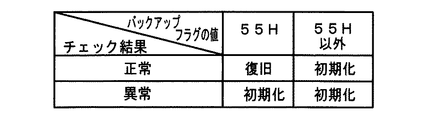
この実施の形態では、バックアップRAM領域にバックアップデータがあるか否かは、電力供給停止時処理においてバックアップRAM領域に設定されるバックアップフラグの状態によって確認される。この例では、図20に示すように、バックアップフラグ領域に「55H」が設定されていればバックアップあり(オン状態)を意味し、「55H」以外の値が設定されていればバックアップなし(オフ状態)を意味する。
【0140】
バックアップありを確認したら、CPU56は、バックアップRAM領域のデータチェック(この例ではパリティチェック)を行う(ステップS9)。この実施の形態では、クリアデータ(00)をチェックサムデータエリアにセットし、チェックサム算出開始アドレスをポインタにセットする。また、チェックサムの対象となるデータ数に対応するチェックサム算出回数をセットする。そして、チェックサムデータエリアの内容とポインタが指すRAM領域の内容との排他的論理和を演算する。演算結果をチェックサムデータエリアにストアするとともに、ポインタの値を1増やし、チェックサム算出回数の値を1減算する。以上の処理が、チェックサム算出回数の値が0になるまで繰り返される。チェックサム算出回数の値が0になったら、CPU56は、チェックサムデータエリアの内容の各ビットの値を反転し、反転後のデータをチェックサムとする。
【0141】
電力供給停止時処理において、上記の処理と同様の処理によってチェックサムが算出され、チェックサムはバックアップRAM領域に保存されている。ステップS9では、算出したチェックサムと保存されているチェックサムとを比較する。不測の停電等の電力供給停止が生じた後に復旧した場合には、バックアップRAM領域のデータは保存されているはずであるから、チェック結果(比較結果)は正常(一致)になる。チェック結果が正常でないということは、バックアップRAM領域のデータが、電力供給停止時のデータとは異なっていることを意味する。そのような場合には、内部状態を電力供給停止時の状態に戻すことができないので、電力供給の停止からの復旧時でない電源投入時に実行される初期化処理を実行する。
【0142】
チェック結果が正常であれば、CPU56は、遊技制御手段の内部状態と表示制御手段等の電気部品制御手段の制御状態を電力供給停止時の状態に戻すための遊技状態復旧処理を行う(ステップS10)。そして、バックアップRAM領域に保存されていたPC(プログラムカウンタ)の退避値がPCに設定され、そのアドレスに復帰する。
【0143】
このように、バックアップフラグとチェックサム等のチェックデータとを用いてバックアップRAM領域のデータが保存されているか否かを確認することによって、遊技状態を電力供給停止時の状態に正確に戻すことができる。すなわち、バックアップRAM領域のデータにもとづく状態復旧処理の確実性が向上する。なお、この実施の形態では、バックアップフラグとチェックデータとの双方を用いてバックアップRAM領域のデータが保存されているか否かを確認しているが、いずれか一方のみを用いてもよい。すなわち、バックアップフラグとチェックデータとのいずれかを、状態復旧処理を実行するための契機としてもよい。
【0144】
また、バックアップフラグの状態によって「バックアップあり」が確認されなかった場合には、後述する遊技状態復旧処理を行うことなく後述する初期化処理を行うようにしているので、バックアップデータが存在しないのにもかかわらず遊技状態復旧処理が実行されてしまうことを防止することができ、初期化処理によって制御状態を初期状態に戻すことが可能となる。
【0145】
さらに、チェックデータを用いたチェック結果が正常でなかった場合には、後述する遊技状態復旧処理を行うことなく後述する初期化処理を行うようにしているので、電力供給停止時とは異なる内容となってしまっているバックアップデータにもとづいて遊技状態復旧処理が実行されてしまうことを防止することができ、初期化処理によって制御状態を初期状態に戻すことが可能となる。
【0146】
初期化処理では、CPU56は、まず、RAMクリア処理を行う(ステップS11)。また、所定の作業領域(例えば、普通図柄判定用乱数カウンタ、普通図柄判定用バッファ、特別図柄左中右図柄バッファ、特別図柄プロセスフラグ、払出コマンド格納ポインタ、賞球中フラグ、球切れフラグ、払出停止フラグなど制御状態に応じて選択的に処理を行うためのフラグ)に初期値を設定する作業領域設定処理を行う(ステップS12)。
【0147】
さらに、CPU56は、所定の払出禁止条件が成立しているか否かを判定し(ステップS13a)、払出禁止条件が成立していなければ、球払出装置97からの払出が可能であることを指示する払出許可状態指定コマンド(以下、払出可能状態指定コマンドという。)を払出制御基板37に対して送信する処理を行う(ステップS13b)。なお、払出禁止条件が成立していれば、主基板31の制御状態を払出禁止状態に設定する。本例では、球切れフラグを球切れ状態を示す状態(オン状態)とするとともに、満タンフラグを下皿満タンを示す状態(オン状態)とすることで、主基板31の制御状態を払出禁止状態に設定する。払出禁止条件は、例えば球切れ状態となっている場合や下皿満タン状態となっている場合など、払い出すべき遊技球を払い出すことができないおそれがある場合や遊技球を払い出すことが適当でない場合に成立する。従って、ステップS13aでは、例えば、球切れスイッチ187による検出状態の確認や、満タンスイッチ48による検出状態の確認が行われる。なお、ステップS13aの判定処理が実行される段階では後述するタイマ割込の設定が行われていないため、ソフトウェアタイマによるウエイト処理などによって監視時間(例えば2ms)を作成し、後述するスイッチの状態を監視する処理(ステップS150〜ステップS159)と同様の処理を実行することで、その監視時間毎に球切れスイッチ187や満タンスイッチ48の状態を監視してスイッチがオンしたか否かを判定するようにすればよい。
【0148】
また、CPU56は、他のサブ基板(ランプ制御基板35、音制御基板70、図柄制御基板80)を初期化するための初期化コマンドを各サブ基板に送信する処理を実行する(ステップS14)。初期化コマンドとして、可変表示装置9に表示される初期図柄を示すコマンド(図柄制御基板80に対して)や賞球ランプ51および球切れランプ52の消灯を指示するコマンド(ランプ制御基板35に対して)等がある。
【0149】
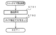
初期化処理では、払出制御基板37に対して、払出禁止条件が成立していない場合に払出可能状態指定コマンドが送信され、払出禁止条件が成立している場合に払出禁止状態指定コマンド(以下、払出禁止状態指定コマンドという。)は送信されない。仮に、遊技機の状態が球払出装置97からの払出が可能でない状態(払出禁止条件が成立している状態)であった場合であっても、払出制御基板37における初期化処理にて払出禁止状態に設定されているはずなので問題はない。なお、払出可能状態指定コマンドおよび他のサブ基板に対する初期化コマンドの送信処理において、例えば、各コマンドが設定されているテーブル(ROM領域)のアドレスをポインタにセットし、後述するコマンドセット処理(図42参照)のような処理ルーチンをコールすればよい。
【0150】
そして、2ms毎に定期的にタイマ割込がかかるようにCPU56に設けられているCTCのレジスタの設定が行われる(ステップS15)。すなわち、初期値として2msに相当する値が所定のレジスタ(時間定数レジスタ)に設定される。
【0151】
初期化処理の実行(ステップS11〜S15)が完了すると、メイン処理で、表示用乱数更新処理(ステップS17)および初期値用乱数更新処理(ステップS18)が繰り返し実行される。表示用乱数更新処理および初期値用乱数更新処理が実行されるときには割込禁止状態とされ(ステップS16)、表示用乱数更新処理および初期値用乱数更新処理の実行が終了すると割込許可状態とされる(ステップS19)。表示用乱数とは、可変表示装置9に表示される図柄を決定するための乱数であり、表示用乱数更新処理とは、表示用乱数を発生するためのカウンタのカウント値を更新する処理である。また、初期値用乱数更新処理とは、初期値用乱数を発生するためのカウンタのカウント値を更新する処理である。初期値用乱数とは、大当りとするか否かを決定するための乱数を発生するためのカウンタ(大当り決定用乱数発生カウンタ)等のカウント値の初期値を決定するための乱数である。後述する遊技制御処理において、大当り決定用乱数発生カウンタのカウント値が1周すると、そのカウンタに初期値が設定される。
【0152】
なお、表示用乱数更新処理が実行されるときには割込禁止状態とされるのは、表示用乱数更新処理が後述するタイマ割込処理でも実行されることから、タイマ割込処理における処理と競合してしまうのを避けるためである。すなわち、ステップS17の処理中にタイマ割込が発生してタイマ割込処理中で表示用乱数を発生するためのカウンタのカウント値を更新してしまったのでは、カウント値の連続性が損なわれる場合がある。しかし、ステップS17の処理中では割込禁止状態にしておけば、そのような不都合が生ずることはない。
【0153】
表示用乱数更新処理における更新値には、例えば、リフレッシュレジスタ(Rレジスタ)によって特定される値が用いられる。Rレジスタは、ダイナミックRAMを用いる場合にリフレッシュカウンタとして使用されるレジスタであり、CPU56は、そのようなRレジスタを内蔵している。また、Rレジスタは、CPU56が命令フェッチを行う毎にインクリメントされる。この場合、CPU56は、変動パターン決定用乱数等を更新する場合にRレジスタの値(1バイト)を参照し、所定の上位ビットをマスクし、残りの下位ビットデータを更新値(表示用乱数を発生するためのカウンタのカウント値に加算される値)として用いる。具体的には、左図柄更新用の乱数が0〜11の範囲で更新される場合であって、加算される更新値として0〜7の範囲の数値が用いられる場合には、左図柄更新用の乱数を更新するときに、Rレジスタの下位3ビットのデータを用いるようにする。Rレジスタの下位3ビットのデータによって、0〜7のランダム値を得ることができるので、簡単な構成でランダム値を更新値とすることができる。また、命令フェッチのタイミングと表示用乱数更新処理の実行タイミングとは同期しないので、Rレジスタの下位ビットを乱数の更新値として用いることにより、表示用乱数を発生するためのカウンタのカウント値をランダムな値にすることができ、出現する表示図柄や変動パターンのランダム性を向上させることができる。また、Rレジスタの機能を利用するので、プログラム構成が単純化され、機種変更などに柔軟に対応できるようになる。さらに、上位ビットをマスクして使用するので、マスクする範囲を変更することで、複数の更新範囲の乱数の更新に対応できる。
【0154】
図21は、遊技状態復旧処理の一例を示すフローチャートである。遊技状態復旧処理において、CPU56は、まず、スタックポインタの復帰処理を行う(ステップS81)。スタックポインタの値は、後で詳述する電力供給停止時処理において、所定のRAMエリア(電源バックアップされている作業領域におけるスタックポインタ退避バッファ)に退避している。よって、ステップS81では、そのRAMエリアの値をスタックポインタに設定することによって復帰させる。具体的には、RAMエリアに退避しているスタック領域のアドレスを示すデータ(スタックアドレスデータ)がスタックポインタに設定される。なお、復帰されたスタックポインタが指す領域(すなわちスタック領域)には、電力供給が停止したときのレジスタ値やプログラムカウンタ(PC)の値が退避している。
【0155】
次いで、CPU56は、払出禁止状態であったか否か確認する(ステップS82)。払出禁止状態であったか否かは、電源バックアップされているRAMエリアに保存されている所定の作業領域(例えば、普通図柄判定用乱数カウンタ、普通図柄判定用バッファ、特別図柄左中右図柄バッファ、特別図柄プロセスフラグ、払出コマンド格納ポインタ、確変フラグ、賞球中フラグ、球切れフラグ、満タンフラグ、払出停止フラグなど)における払出状態データとしての払出停止フラグによって確認される。払出停止フラグは、球切れフラグまたは満タンフラグのいずれか一方がオン状態となったときにオン状態となり、球切れフラグおよび満タンフラグの双方がオフしたときにオフ状態となる。払出禁止状態であった場合には、主基板31の制御状態を払出禁止状態に設定する。本例では、球切れフラグを球切れ状態を示す状態(オン状態)とするとともに、満タンフラグを下皿満タンを示す状態(オン状態)とすることで、主基板31の制御状態を払出禁止状態に設定する。
【0156】
払出禁止状態でなかった場合には、払出制御手段に対して払出が可能であることを指示する払出制御コマンド(払出可能状態指定コマンド)に関するコマンド送信テーブルをセットし(ステップS83)、コマンドセット処理をコールする(ステップS84)。ステップS83では、払出可能状態指定コマンドの払出制御コマンドが格納されているコマンド送信テーブル(ROM)の先頭アドレスが、コマンド送信テーブルのアドレスとして設定される。払出可能状態指定コマンドに関するコマンド送信テーブルには、後述するINTデータ、払出制御コマンドの1バイト目のデータ、および払出制御コマンドの2バイト目のデータが設定されている。なお、ステップS84のコール命令によって、ステップS81にて復帰されているスタックポインタがインクリメントされ、そのスタックポインタが指すスタック領域に、実行されていたプログラムのアドレスデータ(プログラムアドレスデータ)が退避される。そして、コール命令にもとづくコマンドセット処理を終えると、スタックポインタが指しているスタック領域に退避されているアドレスデータ(プログラムアドレスデータ)にもとづいて、コマンドセット処理をコールしたときのアドレスにリターンする。
【0157】
なお、ステップS82にて払出禁止状態であった場合には払出の停止を指示する払出制御コマンド(払出禁止状態指定コマンド)は送信されないが、払出制御基板37における復旧処理(図50参照)にて払出禁止状態に設定されているはずなので問題はない。
【0158】
補給球の不足や余剰球受皿4の満タンについて払出制御手段は認識できないので、遊技制御手段から通知しないと、停電等からの復旧時に、補給球の不足や余剰球受皿4の満タンであるにもかかわらず遊技球の払出処理を開始してしまうおそれがある。しかし、この実施の形態では、補給球の不足や余剰球受皿4の満タンでない場合に、遊技状態復旧処理において払出が可能であること指示する払出制御コマンドが送信されるとともに、その払出制御コマンドを受信しない限り払出制御手段が払出処理を実行しない構成とされているので、補給球の不足や余剰球受皿4の満タンであるにもかかわらず払出制御手段が遊技球の払出処理を開始してしまうことはない。なお、払出制御手段が実行する処理については、あとで詳しく説明する。
【0159】
次いで、CPU56は、電力供給が停止したときの可変表示装置9における特別図柄の表示状態に応じて、その表示状態を復旧させるための表示制御コマンドに関するコマンド送信テーブルをセットし(ステップS85)、コマンドセット処理をコールする(ステップS86)。ステップS85では、表示状態を復旧させるための表示制御コマンドが格納されているコマンド送信テーブル(ROM)の先頭アドレスが、コマンド送信テーブルのアドレスとして設定される。表示状態を復旧させるための表示制御コマンドに関するコマンド送信テーブルには、後述するINTデータ、払出制御コマンドの1バイト目のデータ、および払出制御コマンドの2バイト目のデータが設定されている。
【0160】
ステップS85でセットされる表示制御コマンドには、復旧後に可変表示装置9に表示させる特別図柄を指定する左中右の図柄指定コマンドが含まれる。例えば電力供給が停止したときに特別図柄が変動中であった場合には、その変動後の最終停止図柄を指定する図柄指定コマンドに関するコマンド送信テーブルがセットされ、また、例えば電力供給が停止したときに特別図柄が停止中であった場合には、前回の図柄変動における最終停止図柄を指定する図柄指定コマンドに関するコマンド送信テーブルがセットされる。表示制御用CPU101は、電力供給が開始されたあとに左中右の図柄指定コマンドを受信すると、図柄変動中の表示状態に復旧した場合には、その図柄変動が終了したあと受信した図柄指定コマンドに応じて確定図柄(最終停止図柄)を表示する。また、図柄停止中の表示状態に復旧した場合には、所定の表示タイミングで受信した図柄指定コマンドに応じた確定図柄(前回の図柄変動における確定図柄)を表示する。上記のように、電力供給が開始された場合に、可変表示装置9の表示状態を電源断前の状態から再開させることができるようになる。
【0161】
また、ステップS85でセットされる表示制御コマンドには、確変状態であることを図柄表示基板80に通知するための表示制御コマンド(例えば確変状態指定コマンド)が含まれる。例えば、バックアップされていた確変フラグがオン状態であった場合には、ステップS85にて確変状態であることを示す表示制御コマンドに関するコマンド送信テーブルがセットされる。なお、確変フラグは、高確率状態(大当りが発生しやすい状態)に制御されているときにオン状態とされ、通常状態(大当りが発生する確率が高確率でない状態)に制御されているときはオフ状態とされるフラグであり、バックアップRAM領域に記憶されている。表示制御用CPU101は、確変状態指定コマンドを受信すると、確変時の表示態様(例えば背景の色を確変時の色にする)で表示するように、可変表示装置9の表示制御を行う。上記のように、電力供給が開始された場合に、可変表示装置9の表示状態を電源断前の状態から再開させることができるようになる。
【0162】
次に、CPU56は、2ms毎に定期的にタイマ割込がかかるようにCPU56に設けられているCTCのレジスタの設定を行う(ステップS87)。すなわち、初期値として2msに相当する値が所定のレジスタ(時間定数レジスタ)に設定される。このように、サブ基板に対して制御状態を復旧させるためのコマンドを送信した直後にタイマ割込の設定を行うので、主基板31とサブ基板とで同期をとることが容易となる。
【0163】
その後、CPU56は、バックアップフラグをクリアする(ステップS88)すなわち、前回の電力供給停止時に所定の記憶保護処理が実行されたことを示すフラグをリセットする。よって、制御状態の復旧後に不必要な情報が残存しないようにすることができる。また、スタック領域から各種レジスタの退避値を読み出して、各種レジスタ(IXレジスタ、HLレジスタ、DEレジスタ、BCレジスタ)に設定する(ステップS89)。すなわち、レジスタ復元処理を行う。なお、各レジスタが復元させる毎に、スタックポインタの値が減らされる。すなわち、スタックポインタの値が、スタック領域の1つ前のアドレスを指すように更新される。そして、パリティフラグがオンしていない場合には割込許可状態にする(ステップS90,S91)。最後に、AFレジスタ(アキュミュレータとフラグのレジスタ)をスタック領域から復元する(ステップS92)。
【0164】
そして、RET命令が実行される。RET命令が実行されるときには、CPU56は、スタックポインタが指す領域に格納されているデータをプログラムカウンタに設定することによってプログラムのリターン動作を実現する。ただし、ここでのリターン先は、遊技状態復旧処理をコールした部分ではない。なぜなら、ステップS81においてスタックポインタの復帰処理がなされ、ステップS92でレジスタの復元処理が終了した後では、スタック領域を指すスタックポインタは、NMIによる電力供給停止時処理が開始されたときに実行されていたプログラムのアドレスが退避している領域を指している。すなわち、復帰されたスタックポインタが指すスタック領域に格納されているリターンアドレスは、プログラムにおける前回の電力供給停止時にNMIが発生したアドレスである。従って、ステップS92の次のRET命令によって、電力供給停止時にNMIが発生したアドレスにリターンする。すなわち、本例では、スタック領域に退避されていたアドレスデータ(プログラムアドレスデータ)にもとづいて復旧制御が実行されている。
【0165】
上記のように、遊技状態を復旧させるための制御コマンドを送信する前に、スタックポインタを復帰する構成としているので、コマンドを送信するための処理(コマンドセット処理)をサブルーチンとすることができ、そのサブルーチンをコールすることで遊技状態を復旧させるための制御コマンドの送信処理を実行することができるようになる。
【0166】
スタックポインタを復帰する前の状態においては、スタックポインタは電源投入時に設定される所定の値(例えば0000(H)やFFFF(H))となっている。従って、スタックポインタを復帰することなくサブルーチンのコール命令を行うと、スタックポインタの値が取り得る最高値(例えばFFFF(H))を指していた場合には、コール命令にもとづくスタックポインタの内容のインクリメントを行うことができないという不具合が発生し得る。また、スタックポインタがスタック領域のアドレスを指しているとは限らない(ROM54の領域を指している可能性もある)ので、プログラムカウンタの内容のスタックを行うことができないという不具合も発生し得る。さらに、コール命令にもとづいてプログラムカウンタの内容をスタックすることによって、RAM55にバックアップ記憶されているデータが消去(上書きによる消去)されてしまうという不具合も考えられる。
【0167】
しかし、本例では、上述したようにコマンドを送信する処理を実行する前にスタックポインタを復帰するようにしているので、サブルーチン処理によって遊技状態を復旧させるための制御コマンドの送信処理を実行することができる。従って、遊技制御に用いられるプログラム容量を減らすことができ、ROM54の必要容量を低減させることができる。また、CPU56が、遊技状態復旧処理を効率よく行うことができるようになる。
【0168】
タイマ割込が発生すると、CPU56は、レジスタの退避処理(ステップS20)を行った後、図22に示すステップS21〜S32の遊技制御処理を実行する。ステップS20でのレジスタの退避処理では、実行されていたプログラムのアドレスデータ(プログラムアドレスデータ)をスタックポインタが指すスタック領域に退避する処理も実行される。そして、遊技制御処理を実行したあとのレジスタ復帰処理(ステップS33)にて、スタック領域に退避しているアドレスデータにもとづいて、タイマ割込が発生したときのアドレスに復帰する。遊技制御処理において、CPU56は、まず、スイッチ回路58を介して、ゲートスイッチ32a、始動口スイッチ14a、カウントスイッチ23および入賞口スイッチ29a,30a,33a,39a等のスイッチの検出信号を入力し、それらの状態判定を行う(スイッチ処理:ステップS21)。
【0169】
次いで、パチンコ遊技機1の内部に備えられている自己診断機能によって種々の異常診断処理が行われ、その結果に応じて必要ならば警報が発せられる(エラー処理:ステップS22)。
【0170】
次に、遊技制御に用いられる大当り判定用の乱数等の各判定用乱数を生成するための各カウンタのカウント値を更新する処理を行う(ステップS23)。CPU56は、さらに、表示用乱数および初期値用乱数を生成するためのカウンタのカウント値を更新する処理を行う(ステップS24,S25)。
【0171】
さらに、CPU56は、特別図柄プロセス処理を行う(ステップS26)。特別図柄プロセス制御では、遊技状態に応じてパチンコ遊技機1を所定の順序で制御するための特別図柄プロセスフラグに従って該当する処理が選び出されて実行される。そして、特別図柄プロセスフラグの値は、遊技状態に応じて各処理中に更新される。また、普通図柄プロセス処理を行う(ステップS27)。普通図柄プロセス処理では、普通図柄表示器10の表示状態を所定の順序で制御するための普通図柄プロセスフラグに従って該当する処理が選び出されて実行される。そして、普通図柄プロセスフラグの値は、遊技状態に応じて各処理中に更新される。
【0172】
次いで、CPU56は、特別図柄に関する表示制御コマンドをRAM55の所定の領域に設定して表示制御コマンドを送出する処理を行う(特別図柄コマンド制御処理:ステップS28)。また、普通図柄に関する表示制御コマンドをRAM55の所定の領域に設定して表示制御コマンドを送出する処理を行う(普通図柄コマンド制御処理:ステップS29)。
【0173】
さらに、CPU56は、例えばホール管理用コンピュータに供給される大当り情報、始動情報、確率変動情報などのデータを出力する情報出力処理を行う(ステップS30)。
【0174】
また、CPU56は、所定の条件が成立したときにソレノイド回路59に駆動指令を行う(ステップS31)。可変入賞球装置15または開閉板20を開状態または閉状態としたり、大入賞口内の遊技球通路を切り替えたりするために、ソレノイド回路59は、駆動指令に応じてソレノイド16,21,21Aを駆動する。
【0175】
そして、CPU56は、入賞口スイッチ29a,30a,33a,39aの検出信号にもとづく賞球個数の設定などを行う賞球処理を実行する(ステップS32)。具体的には、入賞口スイッチ29a,30a,33a,39aがオンしたことにもとづく入賞検出に応じて、払出制御基板37に賞球個数を示す払出制御コマンドを出力する。払出制御基板37に搭載されている払出制御用CPU371は、賞球個数を示す払出制御コマンドに応じて球払出装置97を駆動する。その後、CPU56は、レジスタの内容を復帰させ(ステップS33)、割込許可状態に設定する(ステップS34)。
【0176】
以上の制御によって、この実施の形態では、遊技制御処理は2ms毎に起動されることになる。なお、この実施の形態では、タイマ割込処理で遊技制御処理が実行されているが、タイマ割込処理では例えば割込が発生したことを示すフラグのセットのみがなされ、遊技制御処理はメイン処理において実行されるようにしてもよい。
【0177】
図23〜図25は、電源基板910からの電源断信号に応じて実行されるマスク不能割込処理(電力供給停止時処理)の処理例を示すフローチャートである。なお、マスク不能割込処理とは、割込禁止がかけられない処理を意味する。マスク不能割込が発生すると、CPU56に内蔵されている割込制御機構は、マスク不能割込発生時に実行されていたプログラムのアドレス(具体的には実行完了後の次のアドレス)を、スタックポインタが指すスタック領域に退避させるとともに、スタックポインタの値を増やす。すなわち、スタックポインタの値がスタック領域の次のアドレスを指すように更新する。
【0178】
電力供給停止時処理において、CPU56は、AFレジスタ(アキュミュレータとフラグのレジスタ)を所定のバックアップRAM領域に退避する(ステップS451)。また、割込フラグをパリティフラグにコピーする(ステップS452)。パリティフラグはバックアップRAM領域に形成されている。また、BCレジスタ、DEレジスタ、HLレジスタ、IXレジスタおよびスタックポインタをバックアップRAM領域に退避する(ステップS454〜S458)。なお、電源復旧時には、退避された内容にもとづいてレジスタ内容が復元され、パリティフラグの内容に応じて、割込許可状態/禁止状態の内部設定がなされる。なお、S458ではスタックポインタが退避されるが、さらに詳しく言えば、スタックポインタに設定されているスタック領域のアドレスを示すデータ(スタックアドレスデータ)がバックアップRAM領域に退避される。
【0179】
次いで、CPU56は、クリアデータ(00)を適当なレジスタにセットし(ステップS459)、処理数(この例では「7」)を別のレジスタにセットする(ステップS460)。また、出力ポート0のアドレスをIOポインタに設定する(ステップS461)。IOポインタとして、さらに別のレジスタが用いられる。
【0180】
そして、IOポインタが指すアドレスにクリアデータをセットするとともに(ステップS462)、IOポインタの値を1増やし(ステップS463)、処理数の値を1減算する(ステップS464)。ステップS462〜S464の処理が、処理数の値が0になるまで繰り返される(ステップS465)。その結果、全ての出力ポート0〜6(図16および図17参照)にクリアデータが設定される。図16および図17に示すように、この例では、「1」がオン状態であり、クリアデータである「00」が各出力ポートにセットされるので、全ての出力ポートがオフ状態になる。
【0181】
上記のように、各出力ポートがオフ状態になるので、保存される遊技状態と整合しない状況が発生することは確実に防止される。つまり、パチンコ遊技機のように可変入賞球装置を有している遊技機において、実装の関係上、可変入賞球装置における可変入賞口の位置と入賞を検出する入賞口スイッチの設置位置とを、ある程度離さざるを得ない。出力ポート、特に可変入賞球装置を開放状態にするための信号が出力される出力ポートを直ちにオフ状態にしないと、電力供給停止時に、可変入賞口に入賞したにもかかわらず、電力供給停止時処理の実行が開始されて入賞口スイッチの検出がなされない状況が起こりうる。その場合、可変入賞口に入賞があったことは保存されない。すなわち、実際に生じている遊技状態(入賞があったこと)と保存される遊技状態とが整合しない。しかし、この実施の形態では、出力ポートがクリアされて可変入賞球装置が閉じられるので、保存される遊技状態と整合しない状況が発生することは確実に防止される。
【0182】
また、電気部品の駆動が不能になる状態になる前に実行される電力供給停止時処理の際に、出力ポートをクリアすることができるので、電気部品の駆動が不能になる状態となる前に遊技制御手段によって制御される各電気部品を、適切な動作停止状態にすることができる。例えば、開放中の大入賞口を閉成させ、また開放中の可変入賞球装置15を閉成させるなど、電気部品についての作動を停止させたあとに電気部品の駆動が不能になる状態とすることができる。従って、適切な停止状態で電力供給の復旧を待つことが可能となる。
【0183】
さらに、電力供給停止時処理の際に、各電気部品を動作停止状態にするので、各電気部品を駆動するために電力が費やされることがなくなり、また、出力ポートからの信号出力に用いられる電流が遮断されるので、微量ではあるが電力消費を抑えることができる。
【0184】
さらに、この実施の形態では、所定期間(以下、払出確認期間という)、賞球カウントスイッチ301Aの検出信号をチェックする。そして、賞球カウントスイッチ301Aがオンしたら総賞球数バッファの内容を1減らす。
【0185】
なお、この実施の形態では、払出確認期間を計測するために、払出確認期間計測用カウンタが用いられる。払出確認期間計測用カウンタの値は、初期値mから、以下に説明するスイッチ検出処理のループ(S467から始まってS467に戻るループ)が1回実行される毎に−1され、その値が0になると、払出確認期間が終了したとする。検出処理のループでは、例外はあるがほぼ一定の処理が行われるので、ループの1周に要する時間のm倍の時間が、ほぼ払出確認期間に相当する。
【0186】
払出確認期間を計測するために、CPU56の内蔵タイマを用いてもよい。すなわち、スイッチ検出処理開始時に、内蔵タイマに所定値(払出確認期間に相当)を設定しておく。そして、スイッチ検出処理のループが1回実行される毎に、内蔵タイマのカウント値をチェックする。そして、カウント値が0になったら、払出確認期間が終了したとする。内蔵タイマの値が0になったことを検出するために内蔵タイマによる割込を用いることもできるが、この段階では制御内容(RAMに格納されている各値など)を変化させないように、割込を用いず、内蔵タイマのカウント値を読み出してチェックするようなプログラム構成の方が好ましい。
【0187】
また、払出確認期間は、遊技球が、球払出装置97から落下した時点(例えば図5に示すスプロケット292の下方の球通路293a,293bに送り出された時点)から、賞球カウントスイッチ301Aに到達するまでの時間以上に設定される。球払出装置97から賞球カウントスイッチ301Aまでの距離をLとすると、その間の落下時間tは、t=√(2L/g)(g:重力加速度)になるので、払出確認期間は、それ以上に設定される。払出確認期間の具体的な値は、距離Lの値や、落下時間tからどの程度余裕を持たせるかによって異なるが、例えば100[ms]〜150[ms]程度とされる。
【0188】
遊技制御手段において貸し球の払出検出を行う場合にも、同様にして、払出確認期間が設定される。すなわち、遊技球が、球払出装置97から落下した時点(例えば図5に示すスプロケット292の下方の球通路293a,293bに送り出された時点)から、球貸しカウントスイッチ301Bに到達するまでの時間以上に設定される。従って、球払出装置97から球貸しカウントスイッチ301Bまでの距離をLとすると、その間の落下時間tは、やはりt=√(2L/g)(g:重力加速度)になるので、払出確認期間はそれ以上に設定される。この場合にも、払出確認期間の具体的な値は距離Lの値や、落下時間tからどの程度余裕を持たせるかによって異なるが、例えば100[ms]〜150[ms]程度とされる。
【0189】
なお、球払出装置97から賞球カウントスイッチ301Aまでの距離と貸し球カウントスイッチ301Bまでの距離とが異なる場合には、球払出装置97からの距離が離れているスイッチの距離にもとづいて払出確認期間を定めるようにすればよい。
【0190】
少なくとも、スイッチ検出処理が実行される払出確認期間では、賞球カウントスイッチ301Aが遊技球を検出できる状態でなければならない。そこで、この実施の形態では、図11に示されたように、電源基板910におけるコンバータIC920の入力側に比較的大容量の補助駆動電源としてのコンデンサ923が接続されている。よって、遊技機に対する電力供給停止時にも、ある程度の期間は+12V電源電圧がスイッチ駆動可能な範囲に維持され、賞球カウントスイッチ301Aが動作可能になる。その期間が、上記の払出確認期間以上になるように、コンデンサ923の容量が決定される。
【0191】
なお、入力ポートおよびCPU56も、コンバータIC920で作成される+5V電源で駆動されるので、電力供給停止時にも、比較的長い期間動作可能になっている。
【0192】
上記のように、この例では、払出確認期間計測用カウンタに初期値mが設定される(ステップS466)。また、ステップS467において、2ms計測用カウンタに2msの時間に相当する初期値nが設定される。そして、2ms計測用カウンタの値が0になるまで(ステップS468)、2ms計測用カウンタの値が−1される(ステップS469)。
【0193】
2ms計測用カウンタの値が0になると、賞球カウントスイッチ301Aの検出信号の入力チェックが行われる。すなわち、後述するスイッチ処理およびスイッチチェック処理に類似した処理が行われる。具体的には、入力ポート1に入力されているデータを入力する(ステップS470)。次いで、クリアデータ(00)をセットする(ステップS471)。また、ポート入力データ、この場合には入力ポート1からの入力データを「比較値」として設定する(ステップS472)。さらに、賞球カウントスイッチ301Aのためのスイッチタイマのアドレスをポインタにセットする(ステップS473)。
【0194】
そして、ポインタ(スイッチタイマのアドレスが設定されている)が指すスイッチタイマをロードするとともに(ステップS474)、比較値を右(上位ビットから下位ビットへの方向)にシフトする(ステップS475)。比較値には入力ポート1のデータ設定されている。そして、この場合には、賞球カウントスイッチ301Aの検出信号がキャリーフラグに押し出される。
【0195】
キャリーフラグの値が「1」であれば(ステップS476)、すなわち賞球カウントスイッチ301Aの検出信号がオン状態であれば、スイッチタイマの値を1加算する(ステップS477)。キャリーフラグの値が「0」であれば、すなわち賞球カウントスイッチ301Aの検出信号がオフ状態であれば、スイッチタイマにクリアデータをセットする(ステップS478)。すなわち、スイッチがオフ状態であれば、スイッチタイマの値が0に戻る。
【0196】
そして、スイッチタイマの値が2になったときに(ステップS479)、総賞球数格納バッファの格納値を1減算するとともに(ステップS480)、賞球情報カウンタの値を+1する(ステップS481)。そして、賞球情報カウンタの値が10以上であれば(ステップS482)、賞球情報出力カウンタの値を+1するとともに(ステップS483)、賞球情報カウンタの値を−10する(ステップS484)。
【0197】
次いで、払出確認期間計測用カウンタの値を−1し(ステップS485)、その値が0になっていなければステップS467に戻る。
【0198】
以上の処理によって、払出確認期間内に賞球カウントスイッチ301Aがオンしたら、総賞球数格納バッファの値が−1される。バックアップRAMの内容を保存するための処理は、このようなスイッチ検出処理の後で行われるので、払出が完了した賞球について、必ず総賞球数格納バッファが−1される。従って、遊技球の払出に関して、保存される制御状態に矛盾が生じてしまうことが防止される。また、スイッチ検出処理において、遊技機外部への賞球情報出力のための賞球情報出力回数カウンタの演算も行われるので、外部に出力される賞球情報と実際の払出賞球数とが食い違ってしまうようなこともない。
【0199】
また、上記のスイッチ検出処理では、検出期間用カウンタを用いたタイマ処理が施されている。すなわち、2ms毎に賞球カウントスイッチ301Aの検出出力のチェックが行われ、2回連続してオン検出した場合に、賞球カウントスイッチ301Aが確実にオンしたと見なされる。すなわち、所定の遊技媒体検出判定期間(電力供給停止時処理において、遊技媒体(ここでは払い出された賞球)の検出の有無を判定するための期間。本例では、2ms以上の期間)の前後に2回連続してオン検出した場合に、1個の賞球の払出が完了したと見なされる。このように、本例では、遊技媒体検出判定期間を、通常遊技媒体検出判定期間(電力供給停止時処理での処理でない、通常の遊技状態において遊技媒体の有無を判定するための期間。本例では、後述するスイッチオン判定値(図35参照)によって決定される2ms以上の期間であって、後述する図33のステップS188の判断で用いられている。)と同じ期間としている。従って、通常の制御と同一の条件の下で、賞球カウントスイッチ301Aがオンしたか否かを判定することができる。また、通常の制御と同一の条件の下、同一の処理によって賞球カウントスイッチ301Aがオンしたか否かを判定するので、電力供給停止時処理でのスイッチ検出の処理モジュールと、通常の制御におけるスイッチ検出の処理モジュール(図29の処理や図30の処理を含む図22のステップS21の処理モジュール)を、共通の処理モジュールとすることができる。すなわち、通常の制御におけるスイッチ検出の処理モジュールを、電力供給停止時処理でのスイッチ検出の際に利用することができる。なお、遊技媒体検出判定期間は、通常遊技媒体検出判定期間と異なる期間としてもよい。上記のように、2回連続してオン検出した場合に、賞球カウントスイッチ301Aが確実にオンしたと見なされるようにしているため、誤ってスイッチオン検出がなされてしまうことが防止され、払い出された賞球を確実に検出することが可能となる。
【0200】
なお、この実施の形態では、賞球カウントスイッチ301Aのみのスイッチ検出処理が行われたが、始動入賞口のスイッチや大入賞口に関連するV入賞スイッチ22やカウントスイッチについても同様のスイッチ検出処理を行ってもよい。また、他の入賞についても同様のスイッチ検出処理を行ってもよい。そのようなオンチェックも行う場合には、入賞口に遊技球が入賞した直後に停電が発生したような場合でも、その入賞が確実に検出され、保存される遊技状態に反映される。
【0201】
払出確認期間が経過すると(ステップS486)、すなわち、払出確認期間計測用カウンタの値が0になると、バックアップあり指定値(この例では「55H」)をバックアップフラグにストアする(ステップS487)。バックアップフラグはバックアップRAM領域に形成されている。次いで、パリティデータを作成する(ステップS488〜S497)。すなわち、まず、クリアデータ(00)をチェックサムデータエリアにセットし(ステップS488)、チェックサム算出開始アドレスをポインタにセットする(ステップS489)。また、チェックサム算出回数をセットする(ステップS490)。
【0202】
そして、チェックサムデータエリアの内容とポインタが指すRAM領域の内容との排他的論理和を演算する(ステップS491)。演算結果をチェックサムデータエリアにストアするとともに(ステップS492)、ポインタの値を1増やし(ステップS493)、チェックサム算出回数の値を1減算する(ステップS494)。ステップS491〜S494の処理が、チェックサム算出回数の値が0になるまで繰り返される(ステップS495)。
【0203】
チェックサム算出回数の値が0になったら、CPU56は、チェックサムデータエリアの内容の各ビットの値を反転する(ステップS496)。そして、反転後のデータをチェックサムデータエリアにストアする(ステップS497)。このデータが、電源投入時にチェックされるパリティデータとなる。次いで、RAMアクセスレジスタにアクセス禁止値を設定する(ステップS498)。以後、内蔵RAM55のアクセスができなくなる。
【0204】
そして、RAMアクセスレジスタにアクセス禁止値を設定すると、CPU56は、待機状態(ループ状態)に入る。従って、システムリセットされるまで、何もしない状態になる。
【0205】
この実施の形態では、遊技制御処理において用いられるデータが格納されるRAM領域は全て電源バックアップされている。従って、その内容が正しく保存されているか否かを示すチェックサムの生成処理、およびその内容を書き換えないようにするためのRAMアクセス防止処理が、遊技状態を保存するための処理に相当する。
【0206】
なお、この実施の形態では、NMIに応じて電力供給停止時処理が実行されたが、電源断信号をCPU56のマスク可能端子に接続し、マスク可能割込処理によって電力供給停止時処理を実行してもよい。また、電源断信号を入力ポートに入力し、入力ポートのチェック結果に応じて電力供給停止時処理を実行してもよい。
【0207】
また、この実施の形態では、電源断信号に応じて起動される処理の最初にレジスタの保存処理が行われたが、スイッチ検出処理においてレジスタを使用しない場合には、スイッチ検出処理の実行後に、すなわち、バックアップフラグの設定とチェックサムの算出の処理の前にレジスタ保存処理を行うことができる。その場合には、レジスタ保存処理、バックアップフラグ設定処理、チェックサム算出処理および出力ポートのオフ設定処理を電力供給停止時処理と見なすことができる。さらに、スイッチ検出処理において幾つかのレジスタを使用する場合であっても、使用しないレジスタについては、バックアップフラグの設定とチェックサムの算出の処理の前にレジスタ保存処理を行うことができる。
【0208】
なお、上記の例では、出力ポートのクリア処理を、スイッチ検出処理の実行前(ステップS466の前)に行っている。電力供給停止時処理の実行中では、CPU56やスイッチ類はコンデンサ923,924の充電電力等で駆動されることになる。出力ポートのクリア処理をスイッチ検出処理の実行前に行っているので、大入賞口や可変入賞装置等がソレノイド等の電気部品で駆動されるように構成されていても、それらが駆動されることはなく、コンデンサ(特にコンデンサ924)の充電電力等を電力供給停止時処理のために効果的に使用することができる。
【0209】
なお、上記の例において、電源が断することが検出された後にV入賞スイッチ22を検出する場合には、ソレノイド21(大入賞口をV入賞スイッチに誘導するための部材を動作させるもの)の出力ポートについては、スイッチ検出処理の実行後にクリアする。そのようにすれば、継続権発生の条件であるV入賞をしていない状態で停電が発生した場合、停電発生直前に大入賞口に入った遊技球をV入賞スイッチ22の側に誘導することができる。従って、不当な継続権の消滅を防止することができる。この場合、上記の払出確認期間の相当する期間は、大入賞口に入賞した遊技球がV入賞スイッチ22に到達するまでの時間以上の所定期間である。なお、ラッチ式のソレノイドを用いた場合には、出力ポートのクリア処理は不要である。
【0210】
また、出力ポートのクリアによって大入賞口が閉じた場合でも、大入賞口内に遊技球があることも考えられるので、電源断信号に応じて実行されるスイッチ検出処理において、カウントスイッチ23の検出も行うことが望ましい。上記の例外的な処理については、第1種パチンコ遊技機においてのみならず、第2種パチンコ遊技機や第3種パチンコ遊技機についても同様である。
【0211】
図26は、遊技機への電力供給停止時の電源電圧低下やNMI信号(=電源断信号:電力供給停止時信号)の様子を示すタイミング図である。遊技機に対する電力供給が停止すると、最も高い直流電源電圧であるVSLのうちの監視電圧(電源監視用IC902に入力される電圧)の電圧値は徐々に低下する。そして、この例では、+22Vにまで低下すると、電源基板910に搭載されている電源監視用IC902から電源断信号が出力される(ローレベルになる)。
【0212】
電源断信号は、電気部品制御基板(この実施の形態では主基板31および払出制御基板37)に導入され、CPU56および払出制御用CPU371のNMI端子に入力される。CPU56および払出制御用CPU371は、NMI処理によって、所定の電力供給停止時処理を実行する。
【0213】
VSLの電圧値がさらに低下して所定値(この例では+9V)にまで低下すると、主基板31や払出制御基板37に搭載されているシステムリセット回路の出力がローレベルになり、CPU56および払出制御用CPU371がシステムリセット状態になる。なお、CPU56および払出制御用CPU371は、システムリセット状態とされる前に、電力供給停止時処理を完了している。
【0214】
VSLの電圧値がさらに低下してVcc(各種回路を駆動するための+5V)を生成することが可能な電圧を下回ると、各基板において各回路が動作できない状態となる。しかし、少なくとも主基板31や払出制御基板37では、電力供給停止時処理が実行され、CPU56および払出制御用CPU371がシステムリセット状態とされている。
【0215】
以上のように、この実施の形態では、電源監視回路は、遊技機で使用される直流電圧のうちで最も高い電源VSLの電圧を監視して、その電源の電圧が所定値を下回ったら電圧低下信号(電源断検出信号)を発生する。図26に示すように、電源断信号が出力されるタイミングでは、IC駆動電圧は、まだ各種回路素子を十分駆動できる電圧値になっている。従って、IC駆動電圧で動作する主基板31のCPU56が所定の電力供給停止時処理を行うための動作時間が確保されている。
【0216】
なお、ここでは、電源監視回路は、遊技機で使用される直流電圧のうちで最も高い電源VSLから分岐された電圧を監視したが、電源断信号を発生するタイミングが、IC駆動電圧で動作する電気部品制御手段が所定の電力供給停止時処理を行うための動作時間が確保されるようなタイミングであれば、監視対象電圧は、最も高い電源VSLの電圧でなくてもよい。すなわち、少なくともICやソレノイドの駆動電圧よりも高い電圧を監視すれば、電気部品制御手段が所定の電力供給停止時処理を行うための動作時間が確保されるようなタイミングで電源断信号を発生することができる。この例では、ソレノイド等の駆動電圧として電源VSLから分岐された電圧が用いられるが、監視対象電圧が供給されるラインとは異なり、ソレノイド等に駆動電圧を供給するラインに大容量のコンデンサ924が接続されているので、ソレノイド等に対する駆動電圧の供給を継続することができる所定期間が確保されているタイミングで電源断信号を発生することができる。
【0217】
最も高い電源VSL以外の電圧を監視対象電圧とする場合、上述したように、監視対象電圧は、電力供給停止時のスイッチオン誤検出の防止も期待できる電圧であることが好ましい。すなわち、遊技機の各種スイッチに供給される電圧(スイッチ電圧:例えば賞球カウントスイッチ301A、球貸しカウントスイッチ301B)が+12Vであることから、+12V電源電圧が落ち始める以前の段階で、電圧低下を検出できることが好ましい。よって、少なくともスイッチ電圧よりも高い電圧を監視することが好ましい。
【0218】
図27は、払出検出手段からの検出信号の入力処理が実行される様子の一例を示すタイミング図である。この実施の形態では、電源断信号は、主基板31および払出制御基板37に入力され、主基板31のCPU56および払出制御用CPU371のNMI端子に入力される。主基板31のCPU56は、マスク不能割込処理によって、上述した電力供給停止時処理を実行する。
【0219】
図27に示すように、電源断信号がオン(この例ではハイレベルからローレベルに変化)するあたりで賞球払出が実行された場合、払出検出手段からの検出信号の入力処理が実行される払出確認期間(検出維持期間)内で賞球カウントスイッチ301Aがオンする。従って、電源断信号がオンするあたりで実行された球払出についても、電力供給停止時処理が実行される際に、総賞球数バッファに反映することができる。
【0220】
VSLの電圧値がさらに低下して所定値(この例では+9V)にまで低下すると、主基板31に入力されているリセットIC651からの信号がローレベルになり、CPU56がシステムリセット状態になる。なお、CPU56は、システムリセット状態とされる前に、電力供給停止時処理を完了している。
【0221】
VSLの電圧値がさらに低下してVcc(各種回路を駆動するための+5V)を生成することが可能な電圧を下回ると、各基板において各回路が動作できない状態となる。しかし、主基板31では、電力供給停止時処理が実行され、CPU56がシステムリセット状態とされている。
【0222】
なお、払出制御基板37における払出制御用CPU371も、同様に電力供給停止時処理を行った後にシステムリセット状態になる。
【0223】
次に、メイン処理におけるスイッチ処理(ステップS21)の具体例を説明する。この実施の形態では、各スイッチの検出信号のオン状態が所定時間継続すると、確かにスイッチがオンしたと判定されスイッチオンに対応した処理が開始される。所定時間を計測するために、スイッチタイマが用いられる。スイッチタイマは、バックアップRAM領域に形成された1バイトのカウンタであり、検出信号がオン状態を示している場合に2ms毎に+1される。図28に示すように、スイッチタイマは検出信号の数N(クリアスイッチ921の検出信号を除く)だけ設けられている。この実施の形態ではN=13である。また、RAM55において、各スイッチタイマのアドレスは、入力ポートのビット配列順(図18に示された上から下への順)と同じ順序で並んでいる。
【0224】
図29は、遊技制御処理におけるステップS21のスイッチ処理の処理例を示すフローチャートである。なお、スイッチ処理は、図22に示すように遊技制御処理において最初に実行される。スイッチ処理において、CPU56は、まず、入力ポート0に入力されているデータを入力する(ステップS101)。次いで、処理数として「8」を設定し(ステップS102)、入賞口スイッチ33aのためのスイッチタイマのアドレスをポインタにセットする(ステップS103)。そして、スイッチチェック処理サブルーチンをコールする(ステップS104)。
【0225】
図30は、スイッチチェック処理サブルーチンを示すフローチャートである。スイッチチェック処理サブルーチンにおいて、CPU56は、ポート入力データ、この場合には入力ポート0からの入力データを「比較値」として設定する(ステップS121)。また、クリアデータ(00)をセットする(ステップS122)。そして、ポインタ(スイッチタイマのアドレスが設定されている)が指すスイッチタイマをロードするとともに(ステップS123)、比較値を右(上位ビットから下位ビットへの方向)にシフトする(ステップS124)。比較値には入力ポート0のデータ設定されている。そして、この場合には、入賞口スイッチ33aの検出信号がキャリーフラグに押し出される。
【0226】
キャリーフラグの値が「1」であれば(ステップS125)、すなわち入賞口スイッチ33aの検出信号がオン状態であれば、スイッチタイマの値を1加算する(ステップS127)。加算後の値が0でなければ加算値をスイッチタイマに戻す(ステップS128,S129)。加算後の値が0になった場合には加算値をスイッチタイマに戻さない。すなわち、スイッチタイマの値が既に最大値(255)に達している場合には、それよりも値を増やさない。
【0227】
キャリーフラグの値が「0」であれば、すなわち入賞口スイッチ33aの検出信号がオフ状態であれば、スイッチタイマにクリアデータをセットする(ステップS126)。すなわち、スイッチがオフ状態であれば、スイッチタイマの値が0に戻る。
【0228】
その後、CPU56は、ポインタ(スイッチタイマのアドレス)を1加算するとともに(ステップS130)、処理数を1減算する(ステップS131)。処理数が0になっていなければステップS122に戻る。そして、ステップS122〜S132の処理が繰り返される。
【0229】
ステップS122〜S132の処理は、処理数分すなわち8回繰り返され、その間に、入力ポート0の8ビットに入力されるスイッチの検出信号について、順次、オン状態かオフ状態か否かのチェック処理が行われ、オン状態であれば、対応するスイッチタイマの値が1増やされる。
【0230】
CPU56は、スイッチ処理のステップS105において、入力ポート1に入力されているデータを入力する。次いで、処理数として「4」を設定し(ステップS106)、賞球カウントスイッチ301Aのためのスイッチタイマのアドレスをポインタにセットする(ステップS107)。そして、スイッチチェック処理サブルーチンをコールする(ステップS108)。
【0231】
スイッチチェック処理サブルーチンでは、上述した処理が実行されるので、ステップS122〜S132の処理が、処理数分すなわち4回繰り返され、その間に、入力ポート1の4ビットに入力されるスイッチの検出信号について、順次、オン状態かオフ状態か否かのチェック処理が行われ、オン状態であれば、対応するスイッチタイマの値が1増やされる。
【0232】
なお、この実施の形態では、遊技制御処理が2ms毎に起動されるので、スイッチ処理も2msに1回実行される。従って、スイッチタイマは、2ms毎に+1される。
【0233】
図31〜図33は、遊技制御処理におけるステップS32の賞球処理の一例を示すフローチャートである。この実施の形態では、賞球処理では、賞球払出の対象となる入賞口スイッチ33a,39a,29a,30a、カウントスイッチ23および始動口スイッチ14aが確実にオンしたか否か判定されるとともに、オンしたら賞球個数を示す払出制御コマンドが払出制御基板37に送出されるように制御し、また、満タンスイッチ48および球切れスイッチ187が確実にオンしたか否か判定されるとともに、オンしたら所定の払出制御コマンドが払出制御基板37に送出されるように制御する等の処理が行われる。
【0234】
賞球処理において、CPU56は、入力判定値テーブルのオフセットとして「1」を設定し(ステップS150)、スイッチタイマのアドレスのオフセットとして「9」を設定する(ステップS151)。入力判定値テーブル(図35参照)のオフセット「1」は、入力判定値テーブルの2番目のデータ「50」を使用することを意味する。また、各スイッチタイマは、図18に示された入力ポートのビット順と同順に並んでいるので、スイッチタイマのアドレスのオフセット「9」は満タンスイッチ48に対応したスイッチタイマが指定されることを意味する。そして、スイッチオンチェックルーチンがコールされる(ステップS152)。
【0235】
入力判定値テーブルとは、各スイッチについて、連続何回のオンが検出されたら確かにスイッチがオンしたと判定するための判定値が設定されているROM領域である。入力判定値テーブルの構成例は図35に示されている。図35に示すように、入力判定値テーブルには、上から順に、すなわちアドレス値が小さい領域から順に、「2」、「50」、「250」、「30」、「250」、「1」の判定値が設定されている。また、スイッチオンチェックルーチンでは、入力判定値テーブルの先頭アドレスとオフセット値とで決まるアドレスに設定されている判定値と、スイッチタイマの先頭アドレスとオフセット値とで決まるスイッチタイマの値とが比較され、一致した場合には、例えばスイッチオンフラグがセットされる。
【0236】
スイッチオンチェックルーチンの一例が図34に示されている。スイッチオンチェックルーチンにおいて、満タンスイッチ48に対応するスイッチタイマの値が満タンスイッチオン判定値「50」に一致していればスイッチオンフラグがセットされるので(ステップS153)、満タンフラグがセットされる(ステップS154)。なお、図31には明示されていないが、満タンスイッチ48に対応したスイッチタイマの値が0になると、満タンフラグはリセットされる。
【0237】
また、CPU56は、入力判定値テーブルのオフセットとして「2」を設定し(ステップS155)、スイッチタイマのアドレスのオフセットとして「0A(H)」を設定する(ステップS156)。入力判定値テーブルのオフセット「2」は、入力判定値テーブルの3番目のデータ「250」を使用することを意味する。また、各スイッチタイマは、図18に示された入力ポートのビット順と同順に並んでいるので、スイッチタイマのアドレスのオフセット「0A(H)」は球切れスイッチ187に対応したスイッチタイマが指定されることを意味する。そして、スイッチオンチェックルーチンがコールされる(ステップS157)。
【0238】
スイッチオンチェックルーチンにおいて、球切れスイッチ187に対応するスイッチタイマの値が球切れスイッチオン判定値「250」に一致していればスイッチオンフラグがセットされるので(ステップS158)、球切れフラグがセットされる(ステップS159)。なお、図31には明示されていないが、球切れスイッチ187に対応したスイッチオフタイマが用意され、その値が50になると、球切れフラグはリセットされる。
【0239】
そして、CPU56は、払出禁止状態であるか否か確認する(ステップS160)。払出禁止状態は、払出制御基板37に対して払出を停止すべき状態であることを指示する払出制御コマンドである払出禁止状態指定コマンドを送出した後の状態であり、具体的には、作業領域における払出停止フラグがセットされている状態である。払出禁止状態でなければ、上述した球切れ状態フラグまたは満タンフラグがオンになったか否かを確認する(ステップS161)。
【0240】
いずれかがオン状態に変化したときには、払出停止フラグをセットするとともに(ステップS162)、払出禁止状態指定コマンドに関するコマンド送信テーブルをセットし(ステップS163)、コマンドセット処理をコールする(ステップS164)。ステップS163では、払出禁止状態指定コマンドの払出制御コマンドが格納されているコマンド送信テーブル(ROM)の先頭アドレスが、コマンド送信テーブルのアドレスとして設定される。払出禁止状態指定コマンドに関するコマンド送信テーブルには、後述するINTデータ、払出制御コマンドの1バイト目のデータ、および払出制御コマンドの2バイト目のデータが設定されている。なお、ステップS161において、いずれか一方のフラグが既にオン状態であったときに他方のフラグがオン状態になったときには、ステップS162〜ステップS164の処理は行われない。
【0241】
また、払出禁止状態であれば、球切れ状態フラグおよび満タンフラグがともにオフ状態になったか否かを確認する(ステップS165)。ともにオフ状態となったとき(後述する解除条件が成立したとき)には、払出停止フラグをリセットするとともに(ステップS166)、払出可能状態指定コマンドに関するコマンド送信テーブルをセットし(ステップS167)、コマンドセット処理をコールする(ステップS168)。ステップS167では、払出可能状態指定コマンドの払出制御コマンドが格納されているコマンド送信テーブル(ROM)の先頭アドレスが、コマンド送信テーブルのアドレスとして設定される。払出可能状態指定コマンドに関するコマンド送信テーブルには、後述するINTデータ、払出制御コマンドの1バイト目のデータ、および払出制御コマンドの2バイト目のデータが設定されている。
【0242】
なお、解除条件は、払出禁止状態を解除するための条件であり、払出禁止状態を維持する必要がなくなったときに成立する条件である。本例では、解除条件は、払出禁止状態とされているときに、余剰球受皿4が満タン状態でなく、かつ、球切れ状態でもない状態でない状態となったこととされている。
【0243】
さらに、CPU56は、入力判定値テーブルのオフセットとして「0」を設定し(ステップS169)、スイッチタイマのアドレスのオフセットとして「0」を設定する(ステップS170)。入力判定値テーブルのオフセット「0」は、入力判定値テーブルの最初のデータを使用することを意味する。また、各スイッチタイマは、図18に示された入力ポートのビット順と同順に並んでいるので、スイッチタイマのアドレスのオフセット「0」は入賞口スイッチ33aに対応したスイッチタイマが指定されることを意味する。また、繰り返し数として「4」をセットする(ステップS171)。そして、スイッチオンチェックルーチンがコールされる(ステップS172)。
【0244】
スイッチオンチェックルーチンにおいて、CPU56は、入力判定値テーブル(図35参照)の先頭アドレスを設定する(ステップS281)。そして、そのアドレスにオフセットを加算し(ステップS282)、加算後のアドレスからスイッチオン判定値をロードする(ステップS283)。
【0245】
次いで、CPU56は、スイッチタイマの先頭アドレスを設定し(ステップS284)、そのアドレスにオフセットを加算し(ステップS285)、加算後のアドレスからスイッチタイマの値をロードする(ステップS286)。各スイッチタイマは、図18に示された入力ポートのビット順と同順に並んでいるので、スイッチに対応したスイッチタイマの値がロードされる。
【0246】
そして、CPU56は、ロードしたスイッチタイマの値とスイッチオン判定値とを比較する(ステップS287)。それらが一致すれば、スイッチオンフラグをセットする(ステップ228)。
【0247】
この場合には、スイッチオンチェックルーチンにおいて、入賞口スイッチ33aに対応するスイッチタイマの値がスイッチオン判定値「2」に一致していればスイッチオンフラグがセットされる(ステップS173)。そして、スイッチチェックオンルーチンは、スイッチタイマのアドレスのオフセットが更新されつつ(ステップS178)、最初に設定された繰り返し数分だけ実行されるので(ステップS176,S177)、結局、入賞口スイッチ33a,39a,29a,30aについて、対応するスイッチタイマの値がスイッチオン判定値「2」と比較されることになる。
【0248】
スイッチオンフラグがセットされたら、払い出すべき賞球個数としての「10」をリングバッファに設定する(ステップS174)。そして、総賞球数格納バッファの格納値(未払出数データ)に10を加算する(ステップS175)。なお、リングバッファにデータを書き込んだときには、書込ポインタをインクリメントし、リングバッファの最後の領域にデータを書き込まれたときには、書込ポインタを、リングバッファの最初の領域を指すように更新する。
【0249】
総賞球数格納バッファは、払出制御手段に対して指示した賞球個数の累積値(ただし、払い出しがなされると減算される)が格納されるバッファであり、バックアップRAMに形成されている。なお、この実施の形態では、リングバッファにデータを書き込んだ時点で総賞球数格納バッファの格納値に対する加算処理が行われるが、払い出すべき賞球個数を指示する払出制御コマンドを出力ポートに出力した時点で総賞球数格納バッファの格納値に対する、出力する払出制御コマンドに対応した賞球数の加算処理を行ってもよい。
【0250】
次に、CPU56は、入力判定値テーブルのオフセットとして「0」を設定し(ステップS179)、スイッチタイマのアドレスのオフセットとして「5」を設定する(ステップS180)。入力判定値テーブルのオフセット「0」は、入力判定値テーブルの最初のデータを使用することを意味する。また、各スイッチタイマは、図18に示された入力ポートのビット順と同順に並んでいるので、スイッチタイマのアドレスのオフセット「5」は始動口スイッチ14aに対応したスイッチタイマが指定されることを意味する。そして、スイッチオンチェックルーチンがコールされる(ステップS181)。
【0251】
スイッチオンチェックルーチンにおいて、始動口スイッチ14aに対応するスイッチタイマの値がスイッチオン判定値「2」に一致していればスイッチオンフラグがセットされる(ステップS182)。スイッチオンフラグがセットされたら、払い出すべき賞球個数としての「6」をリングバッファに設定する(ステップS183)。また、総賞球数格納バッファの格納値に6を加算する(ステップS184)。
【0252】
次いで、CPU56は、入力判定値テーブルのオフセットとして「0」を設定し(ステップS185)、スイッチタイマのアドレスのオフセットとして「6」を設定する(ステップS186)。入力判定値テーブルのオフセット「0」は、入力判定値テーブルの最初のデータを使用することを意味する。また、各スイッチタイマは、図18に示された入力ポートのビット順と同順に並んでいるので、スイッチタイマのアドレスのオフセット「6」はカウントスイッチ23に対応したスイッチタイマが指定されることを意味する。そして、スイッチオンチェックルーチンがコールされる(ステップS187)。
【0253】
スイッチオンチェックルーチンにおいて、カウントスイッチ23に対応するスイッチタイマの値がスイッチオン判定値「2」に一致していればスイッチオンフラグがセットされる(ステップS188)。スイッチオンフラグがセットされたら、払い出すべき賞球個数としての「15」をリングバッファに設定する(ステップS189)。また、総賞球数格納バッファの格納値に15を加算する(ステップS190)。
【0254】
そして、リングバッファにデータが存在する場合には(ステップS191)、読出ポインタが指すリングバッファの内容を送信バッファにセットするとともに(ステップS192)、読出ポインタの値を更新(リングバッファの次の領域を指すように更新)し(ステップS193)、賞球個数に関するコマンド送信テーブルをセットし(ステップS194)、コマンドセット処理をコールする(ステップS195)。コマンドセット処理の動作については後で詳しく説明する。
【0255】
ステップS194では、賞球個数に関する払出制御コマンドが格納されているコマンド送信テーブル(ROM)の先頭アドレスが、コマンド送信テーブルのアドレスとして設定される。賞球個数に関するコマンド送信テーブルには、後述するINTデータ(01(H))、払出制御コマンドの1バイト目のデータ(F0(H))、および払出制御コマンドの2バイト目のデータが設定されている。ただし、2バイト目のデータとして「80(H)」が設定されている。
【0256】
以上のように、遊技制御手段から払出制御基板37に賞球個数を指示する払出制御コマンドを出力しようとするときに、賞球個数に関するコマンド送信テーブルのアドレス設定と送信バッファの設定とが行われる。そして、コマンドセット処理によって、賞球個数に関するコマンド送信テーブルと送信バッファの設定内容とにもとづいて払出制御コマンドが払出制御基板37に送出される。なお、ステップS191において、書込ポインタと読出ポインタとの差によってデータがあるか否か確認することができるが、リングバッファ内の未処理のデータ個数を示すカウンタを設け、カウント値によってデータがあるか否か確認するようにしてもよい。
【0257】
そして、総賞球数格納バッファの内容が0でない場合、すなわち、まだ賞球残がある場合には、CPU56は、賞球払出中フラグをオンする(ステップS196,S197)。
【0258】
また、CPU56は、賞球払出中フラグがオンしているときには(ステップS198)、球払出装置97から実際に払い出された賞球個数を監視して総賞球数格納バッファの格納値を減算する賞球個数減算処理を行う(ステップS199)。なお、賞球払出中フラグがオンからオフに変化したときには、ランプ制御基板35に対して、賞球ランプ51の点灯を指示するランプ制御コマンドが送出される。
【0259】
なお、払出制御手段は、払出禁止状態指定コマンドを受信すると、賞球としての球払出と球貸しとしての球払出とをともに停止させる。また、払出可能状態指定コマンドを受信すると、賞球としての球払出と球貸しとしての球払出とをともに可能な状態とする。しかし、遊技制御手段から払出制御手段に対して、賞球としての球払出を停止または再開させる払出制御コマンドと、球貸しとしての球払出を停止または再開させる払出制御コマンドとを、別の制御コマンドとして送信するようにしてもよい。
【0260】
また、この実施の形態では、払出停止中であっても(ステップS160,S165)、ステップS169〜S195の処理が実行される。すなわち、遊技制御手段は、払出禁止状態であっても、賞球個数を指示するための払出制御コマンドを送出することができる。すなわち、賞球個数を指示するためのコマンドが、払出禁止状態であっても払出制御手段に伝達され、払出禁止状態が解除されたときに、早めに賞球払出を開始することができる。また、遊技制御手段において、払出禁止状態における入賞にもとづく賞球個数を記憶するための大きな記憶領域は必要とされない。
【0261】
さらに、この実施の形態では、遊技媒体の払出状況とは無関係に、ステップS169〜S195の処理が実行される。すなわち、遊技制御手段は、前回までに指定した賞球個数の払い出しが完了しているか否かに関わらず、新たな賞球個数を指示するための払出制御コマンドを送信することができる。よって、遊技制御手段の払い出しに関する処理負担を軽減させることができるとともに、賞球の払出処理を迅速に行うことができる。
【0262】
次に、遊技制御手段から各電気部品制御手段に対する制御コマンドの送出方式について説明しておく。遊技制御手段から他の電気部品制御基板(サブ基板)に制御コマンドを出力しようとするときに、コマンド送信テーブルの先頭アドレスの設定が行われる。図36(A)は、コマンド送信テーブルの一構成例を示す説明図である。1つのコマンド送信テーブルは3バイトで構成され、1バイト目にはINTデータが設定される。また、2バイト目のコマンドデータ1には、制御コマンドの1バイト目のMODEデータが設定される。そして、3バイト目のコマンドデータ2には、制御コマンドの2バイト目のEXTデータが設定される。
【0263】
なお、EXTデータそのものがコマンドデータ2の領域に設定されてもよいが、コマンドデータ2には、EXTデータが格納されているテーブルのアドレスを指定するためのデータが設定されるようにしてもよい。例えば、コマンドデータ2のビット7(ワークエリア参照ビット)が0であれば、コマンドデータ2にEXTデータそのものが設定されていることを示す。そのようなEXTデータはビット7が0であるデータである。この実施の形態では、ワークエリア参照ビットが1であれば、EXTデータとして、送信バッファの内容を使用することを示す。なお、ワークエリア参照ビットが1であれば、他の7ビットが、EXTデータが格納されているテーブルのアドレスを指定するためのオフセットであることを示すように構成することもできる。
【0264】
図36(B)は、INTデータの一構成例を示す説明図である。INTデータにおけるビット0は、払出制御基板37に払出制御コマンドを送出すべきか否かを示す。ビット0が「1」であるならば、払出制御コマンドを送出すべきことを示す。従って、CPU56は、例えば賞球処理(メイン処理のステップS32)において、INTデータに「01(H)」を設定する。また、INTデータにおけるビット1は、図柄出制御基板80に表示制御コマンドを送出すべきか否かを示す。ビット1が「1」であるならば、表示制御コマンドを送出すべきことを示す。従って、CPU56は、例えば特別図柄コマンド制御処理(メイン処理のステップS28)において、INTデータに「02(H)」を設定する。
【0265】
INTデータのビット2,3は、それぞれ、ランプ制御コマンド、音制御コマンドを送出すべきか否かを示すビットであり、CPU56は、それらのコマンドを送出すべきタイミングになったら、特別図柄プロセス処理等で、ポインタが指しているコマンド送信テーブルに、INTデータ、コマンドデータ1およびコマンドデータ2を設定する。それらのコマンドを送出するときには、INTデータの該当ビットが「1」に設定され、コマンドデータ1およびコマンドデータ2にMODEデータおよびEXTデータが設定される。
【0266】
この実施の形態では、払出制御コマンドについて、図36(C)に示すように、リングバッファおよび送信バッファが用意されている。そして、賞球処理において、賞球払出条件が成立すると、成立した条件に応じた賞球個数が順次リングバッファに設定される。また、賞球個数に関する払出制御コマンド送出する際に、リングバッファから1個のデータが送信バッファに転送される。なお、図36(C)に示す例では、リングバッファには、12個分の払出制御コマンドに相当するデータが格納可能になっている。すなわち、12個のバッファがある。なお、リングバッファにおけるバッファの数は、賞球を発生させる入賞口の数に対応した数であればよい。同時入賞が発生した場合でも、それぞれの入賞にもとづく払出制御コマンドのデータの格納が可能だからである。
【0267】
図37は、主基板31から他の電気部品制御基板に送出される制御コマンドのコマンド形態の一例を示す説明図である。この実施の形態では、制御コマンドは2バイト構成であり、1バイト目はMODE(コマンドの分類)を表し、2バイト目はEXT(コマンドの種類)を表す。MODEデータの先頭ビット(ビット7)は必ず「1」とされ、EXTデータの先頭ビット(ビット7)は必ず「0」とされる。このように、電気部品制御基板へのコマンドとなる制御コマンドは、複数のデータで構成され、先頭ビットによってそれぞれを区別可能な態様になっている。なお、図37に示されたコマンド形態は一例であって他のコマンド形態を用いてもよい。例えば、1バイトや3バイト以上で構成される制御コマンドを用いてもよい。また、図37では払出制御基板37に送出される払出制御コマンドを例示するが、他の電気部品制御基板に送出される制御コマンドも同一構成である。
【0268】
図38は、各電気部品制御手段に対する制御コマンドを構成する8ビットの制御信号CD0〜CD7とINT信号との関係を示すタイミング図である。図38に示すように、MODEまたはEXTのデータが出力ポート(出力ポート1〜出力ポート4のうちのいずれか)に出力されてから、Aで示される期間が経過すると、CPU56は、データ出力を示す信号であるINT信号をハイレベル(オンデータ)にする。また、そこからBで示される期間が経過するとINT信号をローレベル(オフデータ)にする。さらに、次に送出すべきデータがある場合には、すなわち、MODEデータ送出後では、Cで示される期間をおいてから2バイト目のデータを出力ポートに送出する。2バイト目のデータに関して、A,Bの期間は、1バイト目の場合と同様である。このように、取込信号はMODEおよびEXTのデータのそれぞれについて出力される。
【0269】
Aの期間は、CPU56が、コマンドの送出準備の期間すなわちバッファに送出コマンドを設定する処理に要する期間であるとともに、制御信号線におけるデータの安定化のための期間である。すなわち、制御信号線において制御信号CD0〜CD7が出力された後、所定期間(Aの期間:オフ出力期間の一部)経過後に、取込信号としてのINT信号が出力される。また、Bの期間(オン出力期間)は、INT信号安定化のための期間である。そして、Cの期間(オフ出力期間の一部)は、電気部品制御手段が確実にデータを取り込めるように設定されている期間である。B,Cの期間では、信号線上のデータは変化しない。すなわち、B,Cの期間が経過するまでデータ出力が維持される。
【0270】
この実施の形態では、払出制御基板37への払出制御コマンド、図柄制御基板80への表示制御コマンド、ランプ制御基板35へのランプ制御コマンドおよび音制御基板70への音制御コマンドは、同一のコマンド送信処理ルーチン(共通モジュール)を用いて送出される。そこで、B,Cの期間すなわち1バイト目に関するINT信号が立ち上がってから2バイト目のデータが送出開始されるまでの期間は、コマンド受信処理に最も時間がかかる電気部品制御手段における受信処理時間よりも長くなるように設定される。
【0271】
なお、各電気部品制御手段は、INT信号が立ち上がったことを検知して、例えば割込処理によって1バイトのデータの取り込み処理を開始する。
【0272】
B,Cの期間が、コマンド受信処理に最も時間がかかる電気部品制御手段における受信処理時間よりも長いので、遊技制御手段が、各電気部品制御手段に対するコマンド送出処理を共通モジュールで制御しても、いずれの電気部品制御手段でも遊技制御手段からの制御コマンドを確実に受信することができる。
【0273】
CPU56は、INT信号出力処理を実行した後に所定期間が経過すると次のデータを送出できる状態になるが、その所定期間(B,Cの期間)は、INT信号出力処理の前にデータを送出してからINT信号を出力開始するまでの期間(Aの期間)よりも長い。上述したように、Aの期間はコマンドの信号線における安定化期間であり、B,Cの期間は受信側がデータを取り込むのに要する時間を確保するための期間である。従って、Aの期間をB,Cの期間よりも短くすることによって、受信側の電気部品制御手段が確実にコマンドを受信できる状態になるという効果を得ることができるとともに、1つのコマンドの送出完了に要する期間が短縮される効果もある。
【0274】
図39は、払出制御コマンドの内容の一例を示す説明図である。本例では、払出制御を実行するために、複数種類の払出制御コマンドが用いられる。図39に示された例において、MODE=FF(H),EXT=00(H)のコマンドFF00(H)は、払出が可能であることを指示する払出制御コマンド(払出可能状態指定コマンド)である。MODE=FF(H),EXT=01(H)のコマンドFF01(H)は、払出を禁止すべき状態であることを指示する払出制御コマンド(払出禁止状態指定コマンド)である。また、MODE=F0(H)のコマンドF0XX(H)は、賞球個数を指定する払出制御コマンド(払出個数指定コマンド)である。EXTである「XX」が払出個数を示す。
【0275】
払出制御手段は、主基板31の遊技制御手段からFF01(H)の払出制御コマンドを受信すると賞球払出および球貸しを停止する状態となり、FF00(H)の払出制御コマンドを受信すると賞球払出および球貸しができる状態になる。また、賞球個数を指定する払出制御コマンドを受信すると、受信したコマンドで指定された個数に応じた賞球払出制御を行う。
【0276】
なお、払出制御コマンドは、払出制御手段が認識可能に1回だけ送出される。認識可能とは、この例では、INT信号のレベルが変化することであり、認識可能に1回だけ送出されるとは、この例では、払出制御信号の1バイト目および2バイト目のそれぞれに応じてINT信号が1回だけパルス状(矩形波状)に出力されることである。
【0277】
各電気部品制御基板への制御コマンドを、対応する出力ポート(出力ポート1〜4)に出力する際に、出力ポート0のビット0〜3のうちのいずれかのビットが所定期間「1」(ハイレベル)になるのであるが、INTデータにおけるビット配列と出力ポート0におけるビット配列とは対応している。従って、各電気部品制御基板に制御コマンドを送出する際に、INTデータにもとづいて、容易にINT信号の出力を行うことができる。
【0278】
図40は、図柄制御基板80に送出される表示制御コマンドの内容の一例を示す説明図である。図40に示す例において、コマンド8000(H)〜80XX(H)(X=4ビットの任意の値)は、特別図柄を可変表示する可変表示装置9における特別図柄の変動パターンを指定する表示制御コマンドである。なお、変動パターンを指定するコマンドは変動開始指示も兼ねている。
【0279】
コマンド8F00(H)および8F01(H)は、電源投入時に送出される特別図柄電源投入時指定コマンド(初期表示態様コマンドの一例)および普通図柄電源投入時指定コマンド(初期表示態様コマンドの一例)である。初期表示態様コマンドは、電源供給開始時に可変表示装置9に表示させる識別情報の態様(初期表示態様)を指示するとともに、その初期表示態様の表示を指示するためのコマンドである。具体的には、初期表示態様コマンドは、例えば、初期表示態様を示すデータはキャラクタROM86の所定の領域に保存されていること、およびキャラクタROM86の所定の領域から初期表示態様を示すデータを読み出して可変表示装置9に表示させることを指示するコマンドである。なお、初期表示態様コマンドは、例えば、初期表示態様は「7」、「8」、「9」の特別図柄であること、およびその初期表示態様を可変表示装置9に表示させることを指示するコマンドであるとされていてもよい。なお、普通図柄電源投入時指定コマンドは、表示制御手段が普通図柄変動制御を行う場合に用いられ、普通図柄表示器10がランプ制御手段で制御される場合には、図柄制御基板80には送出されない。表示制御手段は、特別図柄電源投入時指定コマンドを受信すると、初期表示を行う制御を開始する。
【0280】
コマンド91XX(H)、92XX(H)および93XX(H)は、特別図柄の左中右の停止図柄を指定する表示制御コマンドである。また、コマンドA000(H)は、特別図柄の可変表示の停止を指示する表示制御コマンド(確定コマンド)である。
【0281】
コマンドBXXX(H)は、大当り遊技開始から大当り遊技終了までの間に送出される表示制御コマンドである。コマンドB1XX(H)は、大当り遊技中における大入賞口の開放回数(ラウンド数)の表示を指定するための表示制御コマンドである。コマンドB200(H)は、大当り遊技が開始されるときに、大当り遊技の開始を示す表示を指定するための表示制御コマンドである。コマンドB2XX(H)(XX=01以上)は、大当り遊技中における、大入賞口の開放前の表示(例えば、これから実行されるラウンドが何ラウンド目であるかを報知する表示)を指定するための表示制御コマンドである。コマンドB400(H)は、大当り遊技中において、所定のタイミングで所定の回数(例えば各ラウンド間に大当り図柄が表示されるようなタイミングで、ラウンド数−1回)送出されるコマンドであり、大当り図柄の表示を指定する表示制御コマンド(大当り図柄表示コマンド)である。コマンドB500(H)は、非特定大当り(非確変大当り)が終了したことを示す表示を指定するための表示制御コマンドである。コマンドB501(H)は、特定大当り(確変大当り)が終了したことを示す表示を指定するための表示制御コマンドである。また、コマンドCXXX(H)は、特別図柄の変動および大当り遊技に関わらない可変表示装置9の表示状態に関する表示制御コマンドである。そして、コマンドD000(H)〜D400(H)は、普通図柄の変動パターンに関する表示制御コマンドである。
【0282】
図柄制御基板80の表示制御手段は、主基板31の遊技制御手段から上述した表示制御コマンドを受信すると図40に示された内容に応じて可変表示装置9および普通図柄表示器10の表示状態を変更する。
【0283】
図41は、遊技の制御を行う主基板31からランプ制御基板35に送出されるランプ制御コマンドの内容の一例を示す説明図である。ランプ制御コマンドもMODEとEXTの2バイト構成である。図41に示す例において、コマンド80XX(X=4ビットの任意の値)は、可変表示装置9における特別図柄の変動パターンに対応したランプ・LED表示制御パターンを指定するランプ制御コマンドである。また、コマンドA0XX(H)は、特別図柄の可変表示の停止時のランプ・LED表示制御パターンを指示するランプ制御コマンドであり、コマンドBXXX(H)は、大当り遊技開始から大当り遊技終了までの間のランプ・LED表示制御パターンを指示するランプ制御コマンドである。そして、コマンド9001(H)は、客待ちデモンストレーション時のランプ・LED表示制御パターンを指示するランプ制御コマンドである。
【0284】
なお、コマンド8XXX(H)、9XXX(H),AXXX(H)、BXXX(H)およびCXXX(H)は、遊技進行状況に応じて遊技制御手段から送出されるランプ制御コマンドである。ランプ制御手段は、主基板31の遊技制御手段から上述したランプ制御コマンドを受信すると図41に示された内容に応じてランプ・LEDの表示状態を変更する。なお、コマンド8XXX(H)、9XXX(H),AXXX(H)、BXXX(H)およびCXXX(H)は、表示制御コマンドや音声制御コマンドと例えば共通の制御状態において共通に用いられる。
【0285】
コマンドE0XX(H)は、始動記憶表示器18の点灯個数を示すランプ制御コマンドである。例えば、ランプ制御手段は、始動記憶表示器18における「XX(H)」で指定される個数の表示器を点灯状態とする。また、コマンドE1XX(H)は、普通図柄始動記憶表示器41の点灯個数を示すランプ制御コマンドである。例えば、ランプ制御手段は、普通図柄始動記憶表示器41における「XX(H)」で指定される個数の表示器を点灯状態とする。すなわち、それらのコマンドは、保留個数という情報を報知するために設けられている発光体の制御を指示するコマンドである。なお、始動記憶表示器18および普通図柄始動記憶表示器41の点灯個数に関するコマンドが点灯個数の増減を示すように構成されていてもよい。
【0286】
コマンドE200(H)およびE201(H)は、賞球ランプ51の表示状態に関するランプ制御コマンドであり、コマンドE300(H)およびE301(H)は、球切れランプ52の表示状態に関するランプ制御コマンドである。ランプ制御手段は、主基板31の遊技制御手段から「E201(H)」のランプ制御コマンドを受信すると賞球ランプ51の表示状態を賞球残がある場合としてあらかじめ定められた表示状態とし、「E200(H)」のランプ制御コマンドを受信すると賞球ランプ51の表示状態を賞球残がない場合としてあらかじめ定められた表示状態とする。また、主基板31の遊技制御手段から「E300(H)」のランプ制御コマンドを受信すると球切れランプ52の表示状態を球あり中の表示状態とし、「E301(H)」のランプ制御コマンドを受信すると球切れランプ52の表示状態を球切れ中の表示状態とする。すなわち、コマンドE200およびE201(H)は、未賞球の遊技球があることを遊技者等に報知するために設けられている発光体を制御することを示すコマンドであり、コマンドE300(H)およびE301(H)は、補給球が切れていることを遊技者や遊技店員に報知するために設けられている発光体を制御することを示すコマンドである。
【0287】
図42は、コマンドセット処理(ステップS164,S168,S195)の処理例を示すフローチャートである。コマンドセット処理は、コマンド出力処理とINT信号出力処理とを含む処理である。コマンドセット処理において、CPU56は、まず、コマンド送信テーブルのアドレス(送信信号指示手段としてのポインタの内容)をスタック等に退避する(ステップS331)。そして、ポインタが指していたコマンド送信テーブルのINTデータを引数1にロードする(ステップS332)。引数1は、後述するコマンド送信処理に対する入力情報になる。また、コマンド送信テーブルを指すアドレスを+1する(ステップS333)。従って、コマンド送信テーブルを指すアドレスは、コマンドデータ1のアドレスに一致する。
【0288】
そこで、CPU56は、コマンドデータ1を読み出して引数2に設定する(ステップS334)。引数2も、後述するコマンド送信処理に対する入力情報になる。そして、コマンド送信処理ルーチンをコールする(ステップS335)。
【0289】
図43は、コマンド送信処理ルーチンを示すフローチャートである。コマンド送信処理ルーチンにおいて、CPU56は、引数1に設定されているデータすなわちINTデータを、比較値として決められているワークエリアに設定する(ステップS351)。なお、コマンド送信中フラグは、コマンド送信処理中であるか否かを示すフラグであって、RAM55の所定の領域に記憶されている。次いで、CPU56は、送信回数=4を、処理数として決められているワークエリアに設定する(ステップS352)。そして、払出制御信号を出力するためのポート1のアドレスをIOアドレスにセットする(ステップS353)。この実施の形態では、ポート1のアドレスは、払出制御信号を出力するための出力ポートのアドレスである。また、ポート2〜4のアドレスが、表示制御信号、ランプ制御信号、音声制御信号を出力するための出力ポートのアドレスである。
【0290】
次に、CPU56は、比較値を1ビット右にシフトする(ステップS354)。シフト処理の結果、キャリービットが1になったか否か確認する(ステップS355)。キャリービットが1になったということは、INTデータにおける最も右側のビットが「1」であったことを意味する。この実施の形態では4回のシフト処理が行われるのであるが、例えば、払出制御コマンドを送出すべきことが指定されているときには、最初のシフト処理でキャリービットが1になる。
【0291】
キャリービットが1になった場合には、引数2に設定されているデータ、この場合にはコマンドデータ1(すなわちMODEデータ)を、IOアドレスとして設定されているアドレスに出力する(ステップS356)。最初のシフト処理が行われたときにはIOアドレスにポート1のアドレスが設定されているので、そのときに、払出制御コマンドのMODEデータがポート1に出力される。
【0292】
次いで、CPU56は、IOアドレスを1加算するとともに(ステップS357)、処理数を1減算する(ステップS358)。加算前にポート1を示していた場合には、IOアドレスに対する加算処理によって、IOアドレスにはポート2のアドレスが設定される。ポート2は、表示制御コマンドを出力するためのポートである。そして、CPU56は、処理数の値を確認し(ステップS359)、値が0になっていなければ、ステップS354に戻る。ステップS354で再度シフト処理が行われる。
【0293】
2回目のシフト処理ではINTデータにおけるビット1の値が押し出され、ビット1の値に応じてキャリーフラグが「1」または「0」になる。従って、表示制御コマンドを送出すべきことが指定されているか否かのチェックが行われる。同様に、3回目および4回目のシフト処理によって、ランプ制御コマンドおよび音制御コマンドを送出すべきことが指定されているか否かのチェックが行われる。このように、それぞれのシフト処理が行われるときに、IOアドレスには、シフト処理によってチェックされる制御コマンド(払出制御コマンド、表示制御コマンド、ランプ制御コマンド、音制御コマンド)に対応したIOアドレスが設定されている。
【0294】
よって、キャリーフラグが「1」になったときには、対応する出力ポート(ポート1〜ポート4)に制御コマンドが送出される。すなわち、1つの共通モジュールで、各電気部品制御手段に対する制御コマンドの送出処理を行うことができる。
【0295】
また、このように、シフト処理のみによってどの電気部品制御手段に対して制御コマンドを出力すべきかが判定されるので、いずれの電気部品制御手段に対して制御コマンドを出力すべきか判定する処理が簡略化されている。
【0296】
次に、CPU56は、シフト処理開始前のINTデータが格納されている引数1の内容を読み出し(ステップS360)、読み出したデータをポート0に出力する(ステップS361)。この実施の形態では、ポート0のアドレスは、各制御信号についてのINT信号を出力するためのポートであり、ポート0のビット0〜4が、それぞれ、払出制御INT信号、表示制御INT信号、ランプ制御INT信号、音制御INT信号を出力するためのポートである。INTデータでは、ステップS351〜S359の処理で出力された制御コマンド(払出制御コマンド、表示制御コマンド、ランプ制御コマンド、音制御コマンド)に応じたINT信号の出力ビットに対応したビットが「1」になっている。従って、ポート1〜ポート4のいずれかに出力された制御コマンド(払出制御コマンド、表示制御コマンド、ランプ制御コマンド、音制御コマンド)に対応したINT信号がハイレベルになる。
【0297】
次いで、CPU56は、ウェイトカウンタに所定値を設定し(ステップS362)、その値が0になるまで1ずつ減算する(ステップS363,S364)。この処理は、図38に示されたBの期間を設定するための処理である。ウェイトカウンタの値が0になると、クリアデータ(00)を設定して(ステップS365)、そのデータをポート0に出力する(ステップS366)。よって、INT信号はローレベルになる。また、ウェイトカウンタに所定値を設定し(ステップS362)、その値が0になるまで1ずつ減算する(ステップS368,S369)。この処理は、図38に示されたCの期間を設定するための処理である。ただし、実際のCの期間は、ステップS367〜S369で作成される時間に、その後の処理時間(この時点でMODEデータが出力されている場合にはEXTデータを出力するまでに要する制御にかかる時間)が加算された期間となる。このように、Cの期間が設定されることによって、連続してコマンドが送出される場合であっても、一のコマンドの出力完了後、次にコマンドの送出が開始されるまでに所定期間がおかれることになり、コマンドを受信する電気部品制御手段の側で、容易に連続するコマンドの区切りを識別することができ、各コマンドは確実に受信される。
【0298】
従って、ステップS367でウェイトカウンタに設定される値は、Cの期間が、制御コマンド受信対象となる全ての電気部品制御手段が確実にコマンド受信処理を行うのに十分な期間になるような値である。また、ウェイトカウンタに設定される値は、Cの期間が、ステップS357〜S359の処理に要する時間(Aの期間に相当)よりも長くなるような値である。なお、Aの期間をより長くしたい場合には、Aの期間を作成するためのウェイト処理(例えば、ウェイトカウンタに所定値を設定し、ウェイトカウンタの値が0になるまで減算を行う処理)を行う。
【0299】
以上のようにして、制御コマンドの1バイト目のMODEデータが送出される。そこで、CPU56は、図42に示すステップS336で、コマンド送信テーブルを指す値を1加算する。従って、3バイト目のコマンドデータ2の領域が指定される。CPU56は、指し示されたコマンドデータ2の内容を引数2にロードする(ステップS337)。また、コマンドデータ2のビット7(ワークエリア参照ビット)の値が「0」であるか否か確認する(ステップS338)。0でなければ、送信バッファの内容を引数2にロードする(ステップS339)。なお、ワークエリア参照ビットの値が「1」であるときに拡張データを使用するように構成されている場合には、コマンド拡張データアドレステーブルの先頭アドレスをポインタにセットし、そのポインタにコマンドデータ2のビット6〜ビット0の値を加算してアドレスを算出する。そして、そのアドレスが指すエリアのデータを引数2にロードする。
【0300】
送信バッファには賞球個数を特定可能なデータが設定されているので、引数2にそのデータが設定される。なお、ワークエリア参照ビットの値が「1」であるときに拡張データを使用するように構成されている場合には、コマンド拡張データアドレステーブルには、電気部品制御手段に送出されうるEXTデータが順次設定される。よって、ワークエリア参照ビットの値が「1」であれば、コマンドデータ2の内容に応じたコマンド拡張データアドレステーブル内のEXTデータが引数2にロードされる。
【0301】
次に、CPU56は、コマンド送信処理ルーチンをコールする(ステップS340)。従って、MODEデータの送出の場合と同様のタイミングでEXTデータが送出される。
【0302】
以上のようにして、2バイト構成の制御コマンド(払出制御コマンド、表示制御コマンド、ランプ制御コマンド、音制御コマンド)が、対応する電気部品制御手段に送信される。電気部品制御手段ではINT信号の立ち上がりを検出すると制御コマンドの取り込み処理を開始するのであるが、各電気部品制御手段でのコマンド受信処理が完了したあとに終了するように設定されるウエイト期間(ステップS367〜ステップS369の処理によって特定される期間:Cの期間の一部)が経過するまでは新たな信号を出力しないようにしているので、いずれの電気部品制御手段についても、取り込み処理が完了する前に遊技制御手段からの新たな信号が信号線に出力されることはない。すなわち、各電気部品制御手段において、確実なコマンド受信処理が行われる。なお、各電気部品制御手段は、INT信号の立ち下がりで制御コマンドの取り込み処理を開始してもよい。また、INT信号の極性を図37に示された場合と逆にしてもよい。
【0303】
また、この実施の形態では、賞球処理において、賞球払出条件が成立すると賞球個数を特定可能なデータが、同時に複数のデータを格納可能なリングバッファに格納され、賞球個数を指定する払出制御コマンドを送出する際に、読出ポインタが指しているリングバッファの領域のデータが送信バッファに転送される。従って、同時に複数の賞球払出条件の成立があっても、それらの条件成立にもとづく賞球個数を特定可能なデータがリングバッファに保存されるので、各条件成立にもとづくコマンド出力処理は問題なく実行される。
【0304】
さらに、この実施の形態では、1回の賞球処理内で払出禁止状態指定コマンドまたは払出可能状態指定コマンドと賞球個数を示すコマンドとの双方を送出することができる。すなわち、2ms毎に起動される1回の制御期間内において、複数のコマンドを送出することができる。また、この実施の形態では、各制御手段への制御コマンド(表示制御コマンド、ランプ制御コマンド、音制御コマンド、払出制御コマンド)毎に、それぞれ複数のリングバッファが用意されているので、例えば、表示制御コマンド、ランプ制御コマンドおよび音制御コマンドのリングバッファに制御コマンドを特定可能なデータが設定されている場合には、1回のコマンド制御処理で複数の表示制御コマンド、ランプ制御コマンドおよび音制御コマンドを送出するように構成することも可能である。すなわち、同時に(遊技制御処理すなわち2msタイマ割込処理の起動周期での意味)、複数の制御コマンドを送出することができる。遊技演出の進行上、それらの制御コマンドの送出タイミングは同時に発生するので、このように構成されているのは便利である。ただし、払出制御コマンドは、遊技演出の進行とは無関係に発生するので、一般には、表示制御コマンド、ランプ制御コマンドおよび音制御コマンドと同時に送出されることはない。
【0305】
図44は、賞球個数減算処理の一例を示すフローチャートである。賞球個数減算処理において、CPU56は、まず、総賞球数格納バッファの格納値をロードする(ステップS381)。そして、格納値が0であるか否か確認する(ステップS382)。0であれば処理を終了する。
【0306】
0でなければ、賞球カウントスイッチ用のスイッチタイマをロードし(ステップS383)、ロード値とオン判定値(この場合は「2」)とを比較する(ステップS384)。一致したら(ステップS385)、賞球カウントスイッチ301Aが確かにオンしたとして、すなわち、確かに1個の遊技球が球払出装置97から払い出されたとして、総賞球数格納バッファの格納値を1減算する(ステップS386)。
【0307】
また、賞球情報カウンタの値を+1する(ステップS387)。そして、賞球情報カウンタの値が10以上であれば(ステップS388)、賞球情報出力カウンタの値を+1するとともに(ステップS389)、賞球情報カウンタの値を−10する(ステップS390)。なお、賞球情報出力カウンタの値は、図22に示された遊技制御処理における情報出力処理(ステップS30)で参照され、その値が1以上であれば、賞球信号(出力ポート5のビット7:図17参照)として1パルスが出力される。よって、この実施の形態では、10個の遊技球が賞球として払い出される度に、1つの賞球信号が遊技機外部に出力される。
【0308】
そして、総賞球数格納バッファの格納値が0になったら(ステップS391)、賞球払出中フラグをクリアし(ステップS392)、賞球残数がないことを報知するために、ランプ制御コマンド用のコマンド送信テーブルに賞球ランプ51の消灯を示すコマンドデータを設定した後(ステップS393)、ランプ制御コマンドの送出処理を実行する(ステップS394)。
【0309】
次に、遊技制御手段以外の電気部品制御手段の例として、払出制御手段について説明する。
図45は、払出制御用CPU371周りの一構成例を示すブロック図である。図45に示すように、電源基板910の電源監視回路(電源監視手段)からの電源断信号が、バッファ回路980を介して払出制御用CPU371のマスク不能割込端子(XNMI端子)に接続されている。従って、払出制御用CPU371は、マスク不能割込処理によって電源断の発生を確認することができる。また、電源基板910からのリセット信号と復帰信号とはAND回路385に入力され、AND回路385の出力が払出制御用CPU371のリセット端子に入力される。
【0310】
払出制御用CPU371のCLK/TRG2端子には、主基板31からのINT信号が接続されている。CLK/TRG2端子にクロック信号が入力されると、払出制御用CPU371に内蔵されているタイマカウンタレジスタCLK/TRG2の値がダウンカウントされる。そして、レジスタ値が0になると割込が発生する。従って、タイマカウンタレジスタCLK/TRG2の初期値を「1」に設定しておけば、INT信号の入力に応じて割込が発生することになる。なお、INT信号とは、遊技制御手段から払出制御手段に対する払出制御コマンドが送出されたことを意味する信号である。払出制御用CPU371は、INT信号の入力に応じて発生する割込によって、払出制御コマンド受信処理を開始する。
【0311】
図46は、この実施の形態における出力ポートの割り当てを示す説明図である。図46に示すように、出力ポートC(アドレス00H)は、払出モータ289に出力される駆動信号等の出力ポートである。また、出力ポートD(アドレス01H)は、7セグメントLEDであるエラー表示LED374に出力される表示制御信号の出力ポートである。そして、出力ポートE(アドレス02H)は、振分ソレノイド310に出力される駆動信号、およびカードユニット50に対するEXS信号とPRDY信号とを出力するための出力ポートである。
【0312】
図47は、この実施の形態における入力ポートのビット割り当てを示す説明図である。図47に示すように、入力ポートA(アドレス06H)は、主基板31から送出された払出制御コマンドの8ビットの払出制御信号を取り込むための入力ポートである。また、入力ポートB(アドレス07H)のビット0〜1には、それぞれ、賞球カウントスイッチ301Aおよび球貸しカウントスイッチ301Bの検出信号が入力される。ビット2〜5には、カードユニット50からのBRDY信号、BRQ信号、VL信号およびクリアスイッチ921の検出信号が入力される。
【0313】
図48は、払出制御手段(払出制御用CPU371およびROM,RAM等の周辺回路)のメイン処理を示すフローチャートである。メイン処理では、払出制御用CPU371は、まず、必要な初期設定を行う。すなわち、払出制御用CPU371は、まず、割込禁止に設定する(ステップS701)。次に、割込モードを割込モード2に設定し(ステップS702)、スタックポインタにスタックポインタ指定アドレスを設定する(ステップS703)。また、払出制御用CPU371は、内蔵デバイスレジスタの初期化を行い(ステップS704)、CTCおよびPIOの初期化(ステップS705)を行った後に、RAMをアクセス可能状態に設定する(ステップS706)。
【0314】
この実施の形態では、内蔵CTCのうちの一つのチャネルがタイマモードで使用される。従って、ステップS704の内蔵デバイスレジスタの設定処理およびステップS705の処理において、使用するチャネルをタイマモードに設定するためのレジスタ設定、割込発生を許可するためのレジスタ設定および割込ベクタを設定するためのレジスタ設定が行われる。そして、そのチャネルによる割込がタイマ割込として用いられる。タイマ割込を例えば2ms毎に発生させたい場合は、初期値として2msに相当する値が所定のレジスタ(時間定数レジスタ)に設定される。
【0315】
なお、タイマモードに設定されたチャネル(この実施の形態ではチャネル3)に設定される割込ベクタは、タイマ割込処理の先頭アドレスに相当するものである。具体的は、Iレジスタに設定された値と割込ベクタとでタイマ割込処理の先頭アドレスが特定される。タイマ割込処理では、払出制御処理が実行される。
【0316】
また、内蔵CTCのうちの他の一つのチャネル(この実施の形態ではチャネル2)が、遊技制御手段からの払出制御コマンド受信のための割込発生用のチャネルとして用いられ、そのチャネルがカウンタモードで使用される。従って、ステップS704の内蔵デバイスレジスタの設定処理およびステップS705の処理において、使用するチャネルをカウンタモードに設定するためのレジスタ設定、割込発生を許可するためのレジスタ設定および割込ベクタを設定するためのレジスタ設定が行われる。
【0317】
カウンタモードに設定されたチャネル(チャネル2)に設定される割込ベクタは、後述するコマンド受信割込処理の先頭アドレスに相当するものである。具体的は、Iレジスタに設定された値と割込ベクタとでコマンド受信割込処理の先頭アドレスが特定される。
【0318】
この実施の形態では、払出制御用CPU371でも割込モード2が設定される。従って、内蔵CTCのカウントアップにもとづく割込処理を使用することができる。また、CTCが送出した割込ベクタに応じた割込処理開始アドレスを設定することができる。
【0319】
CTCのチャネル2(CH2)のカウントアップにもとづく割込は、上述したタイマカウンタレジスタCLK/TRG2の値が「0」になったときに発生する割込である。従って、例えばステップS705において、特定レジスタとしてのタイマカウンタレジスタCLK/TRG2に初期値「1」が設定される。さらに、CLK/TRG2端子に入力される信号の立ち上がりまたは立ち下がりで特定レジスタとしてのタイマカウンタレジスタCLK/TRG2のカウント値が−1されるのであるが、所定の特定レジスタの設定によって、立ち上がり/立ち下がりの選択を行うことができる。この実施の形態では、CLK/TRG2端子に入力される信号の立ち上がりで、タイマカウンタレジスタCLK/TRG2のカウント値が−1されるような設定が行われる。
【0320】
また、CTCのチャネル3(CH3)のカウントアップにもとづく割込は、CPUの内部クロック(システムクロック)をカウントダウンしてレジスタ値が「0」になったら発生する割込であり、後述する2msタイマ割込として用いられる。具体的には、CPU371の動作クロックを分周したクロックがCTCに与えられ、クロックの入力によってレジスタの値が減算され、レジスタの値が0になるとタイマ割込が発生する。例えば、CH3のレジスタ値はシステムクロックの1/256周期で減算される。分周したクロックにもとづいて減算が行われるので、レジスタの初期値は大きくならない。ステップS705において、CH3のレジスタには、初期値として2msに相当する値が設定される。
【0321】
CTCのCH2のカウントアップにもとづく割込は、CH3のカウントアップにもとづく割込よりも優先順位が高い。従って、同時にカウントアップが生じた場合に、CH2のカウントアップにもとづく割込、すなわち、コマンド受信割込処理の実行契機となる割込の方が優先される。
【0322】
次いで、払出制御用CPU371は、入力ポートB(図47参照)を介して入力されるクリアスイッチ921の出力信号の状態を1回だけ確認する(ステップS707)。その確認においてオンを検出した場合には、払出制御用CPU371は、通常の初期化処理を実行する(ステップS711〜ステップS714)。クリアスイッチ921がオンである場合(押下されている場合)には、ローレベルのクリアスイッチ信号が出力されている。なお、入力ポート372では、クリアスイッチ信号のオン状態はハイレベルである。また、払出制御手段においては、ステップS707の判定を行わなくてもよい。
【0323】
なお、払出制御用CPU371も、主基板31のCPU56と同様に、スイッチの検出信号のオン判定を行う場合には、例えば、オン状態が少なくとも2ms(2ms毎に起動される処理の1回目の処理における検出直前に検出信号がオンした場合)継続しないとスイッチオンとは見なさないが、クリアスイッチ921のオン検出の場合には、1回のオン判定でオン/オフが判定される。すなわち、操作手段としてのクリアスイッチ921が所定の操作状態であるか否かを払出制御用CPU371が判定するための初期化要求検出判定期間は、遊技媒体検出手段としての賞球カウントスイッチ等が遊技媒体を検出したことを判定するための遊技媒体検出判定期間とは異なる期間とされている。
【0324】
クリアスイッチ921がオンの状態でない場合には、払出制御用CPU371は、払出制御用のバックアップRAM領域にバックアップデータが存在しているか否かの確認を行う(ステップS708)。例えば、主基板31のCPU56の処理と同様に、遊技機への電力供給停止時にセットされるバックアップフラグがセット状態になっているか否かによって、バックアップデータが存在しているか否か確認する。バックアップフラグがセット状態になっている場合には、バックアップデータありと判断する。
【0325】
バックアップありを確認したら、払出制御用CPU371は、バックアップRAM領域のデータチェック(この例ではパリティチェック)を行う。不測の停電等の電力供給の停止が生じた後に復旧した場合には、バックアップRAM領域のデータは保存されていたはずであるから、チェック結果は正常になる。チェック結果が正常でない場合には、内部状態を電力供給の停止時の状態に戻すことができないので、不足の停電等からの復旧時ではなく電源投入時に実行される初期化処理を実行する。
【0326】
チェック結果が正常であれば(ステップS709)、払出制御用CPU371は、内部状態を電力供給停止時の状態に戻すための払出状態復旧処理を行う(ステップS710)。そして、バックアップRAM領域に保存されていたPC(プログラムカウンタ)の指すアドレスに復帰する。
【0327】
初期化処理では、払出制御用CPU371は、まず、RAMクリア処理を行う(ステップS711)。そして、2ms毎に定期的にタイマ割込がかかるように払出制御用CPU371に設けられているCTCのレジスタの設定が行われる(ステップS712)。すなわち、初期値として2msに相当する値が所定のレジスタ(時間定数レジスタ)に設定される。また、本例では、払出制御用CPU371は、初期状態として払出禁止状態に設定する(ステップS713)。なお、払出禁止状態に設定するときには、例えば払出モータ289の駆動が停止されるとともに払出停止中であることを示す内部フラグ(払出停止中フラグ)がセットされる。すなわち、ステップS713では、払い出しが禁止された状態であることを示すデータ(セットされた払出停止中フラグ)を所定の記憶領域に記憶する処理が実行されている。払出停止中フラグについては、あとで詳しく説明する。そして、初期設定処理のステップS701において割込禁止とされているので、初期化処理を終える前に割込が許可される(ステップS714)。
【0328】
この実施の形態では、払出制御用CPU371の内蔵CTCが繰り返しタイマ割込を発生するように設定される。この実施の形態では、繰り返し周期は2msに設定される。そして、タイマ割込が発生すると、図49に示すように、タイマ割込があったことを示すタイマ割込フラグがセットされる(ステップS792)。そして、メイン処理において、タイマ割込フラグがセットされたことが検出されたら(ステップS715)、タイマ割込フラグがリセットされるとともに(ステップS751)、払出制御処理(ステップS751〜S760)が実行される。
【0329】
なお、タイマ割込では、図49に示すように、最初に割込許可状態に設定される(ステップS791)。よって、タイマ割込処理中では割込許可状態になり、INT信号の入力にもとづく払出制御コマンド受信処理を優先して実行することができる。
【0330】
払出制御処理において、払出制御用CPU371は、まず、入力ポート372bに入力される賞球カウントスイッチ301Aや球貸しカウントスイッチ301B等のスイッチがオンしたか否かを判定する(スイッチ処理:ステップS752)。
【0331】
次に、払出制御用CPU371は、主基板31から払出禁止状態指定コマンドを受信していたら払出禁止状態に設定し、払出可能状態指定コマンドを受信していたら払出禁止状態の解除を行う(払出禁止状態設定処理:ステップS753)。また、受信した払出制御コマンドを解析し、解析結果に応じた処理を実行する(コマンド解析実行処理:ステップS754)。さらに、プリペイドカードユニット制御処理を行う(ステップS755)。
【0332】
次いで、払出制御用CPU371は、球貸し要求に応じて貸し球を払い出す制御を行う(ステップS756)。このとき、払出制御用CPU371は、振分ソレノイド310によって球振分部材311を球貸し側に設定する。
【0333】
さらに、払出制御用CPU371は、総合個数記憶に格納された個数の賞球を払い出す賞球制御処理を行う(ステップS757)。このとき、払出制御用CPU371は、振分ソレノイド310によって球振分部材311を賞球側に設定する。そして、出力ポート372cおよび中継基板72を介して球払出装置97の払出機構部分における払出モータ289に対して駆動信号を出力し、所定の回転数分払出モータ289を回転させる払出モータ制御処理を行う(ステップS758)。
【0334】
なお、この実施の形態では、払出モータ289としてステッピングモータが用いられ、それらを制御するために1−2相励磁方式が用いられる。従って、具体的には、払出モータ制御処理において、8種類の励磁パターンデータが繰り返し払出モータ289に出力される。また、この実施の形態では、各励磁パターンデータが4msずつ出力される。
【0335】
次いで、エラー検出処理が行われ、その結果に応じてエラー表示LED374に所定の表示を行う(エラー処理:ステップS759)。また、遊技機外部に出力される球貸し個数信号を出力する処理等を行う(出力処理:ステップS760)。
【0336】
なお、図46に示す出力ポートCは、払出制御処理における払出モータ制御処理(ステップS758)でアクセスされる。また、出力ポートDは、払出制御処理におけるエラー処理(ステップS759)でアクセスされる。そして、出力ポートEは、払出制御処理における球貸し制御処理(ステップS756)および賞球制御処理(ステップS757)でアクセスされる。
【0337】
図50は、ステップS710の払出状態復旧処理の一例を示すフローチャートである。払出状態復旧処理において、払出制御用CPU371は、まず、スタックポインタの復帰処理を行う(ステップS731)。スタックポインタの値は、後述する電力供給停止時処理において、所定のRAMエリア(電源バックアップされている)に退避している。よって、ステップS731では、そのRAMエリアの値をスタックポインタに設定することによって復帰させる。なお、復帰されたスタックポインタが指す領域(すなわちスタック領域)には、電力供給が停止したときのレジスタ値やプログラムカウンタ(PC)の値が退避している。
【0338】
次いで、払出制御用CPU371は、復旧する払い出しに関する状態として、本例では払出禁止状態に設定する(ステップS732)。なお、払出禁止状態に設定するときには、例えば払出モータ289の駆動が停止されるとともに払出停止中であることを示す内部フラグ(払出停止中フラグ)がセットされる。すなわち、ステップS732では、払い出しが禁止された状態であることを示すデータ(セットされた払出停止中フラグ)を所定の記憶領域に記憶する処理が実行されている。払出停止中フラグについては、あとで詳しく説明する。
【0339】
また、払出制御用CPU371は、バックアップフラグをクリアする(ステップS733)すなわち、前回の電力供給停止時に所定の記憶保護処理が実行されたことを示すフラグをリセットする。また、スタック領域から各種レジスタの退避値を読み出して、各種レジスタに設定する(ステップS734)。すなわち、レジスタ復元処理を行う。そして、パリティフラグがオンしていない場合には割込許可状態にする(ステップS735,S736)。最後に、AFレジスタ(アキュミュレータとフラグのレジスタ)をスタック領域から復元する(ステップS737)。
【0340】
そして、RET命令が実行されるのであるが、ここでのリターン先は、払出状態復旧処理をコールした部分ではない。なぜなら、ステップS731においてスタックポインタの復帰処理がなされ、復帰されたスタックポインタが指すスタック領域に格納されているリターンアドレスは、プログラムにおける前回の電力供給停止時にNMIが発生したアドレスである。従って、ステップS737の次のRET命令によって、電力供給停止時にNMIが発生したアドレスにリターンする。すなわち、スタック領域に退避されていたアドレスにもとづいて復旧制御が実行されている。
【0341】
図51〜図53は、電源基板910からの電源断信号に応じて実行されるマスク不能割込処理(NMI処理:電力供給停止時処理)の処理例を示すフローチャートである。この例では、NMIに応じて電力供給停止時処理が実行されるが、電源断信号を払出制御用CPU371のマスク可能端子に接続し、マスク可能割込処理によって電力供給停止時処理を実行してもよい。また、電源断信号を入力ポートに入力し、入力ポートのチェック結果に応じて電力供給停止時処理を実行してもよい。
【0342】
マスク不能割込処理において、払出制御用CPU371は、AFレジスタを所定のバックアップRAM領域に退避する(ステップS801)。また、割込フラグをパリティフラグにコピーする(ステップS802)。パリティフラグはバックアップRAM領域に形成されている。また、BCレジスタ、DEレジスタ、HLレジスタ、IXレジスタおよびスタックポインタをバックアップRAM領域に退避する(ステップS804〜808)。なお、電源復旧時には、退避された内容にもとづいてレジスタ内容が復元され、パリティフラグの内容に応じて、割込許可状態/禁止状態の内部設定がなされる。
【0343】
なお、本例では、払出モータ289として、払出制御用CPU371からのパルス信号(駆動信号)によって回転するステッピングモータが用いられている。従って、払出モータ289に対するパルス信号の出力が停止されることによって、球払出装置97の駆動は停止する。
【0344】
次いで、払出制御用CPU371は、クリアデータ(00)を適当なレジスタにセットし(ステップS809)、処理数(この例では「2」)を別のレジスタにセットする(ステップS810)。また、出力ポートCのアドレス(この例では「00H」)をIOポインタに設定する(ステップS811)。IOポインタとして、さらに別のレジスタが用いられる。
【0345】
そして、IOポインタが指すアドレスにクリアデータをセットするとともに(ステップS812)、IOポインタの値を1増やし(ステップS813)、処理数の値を1減算する(ステップS814)。ステップS812〜S814の処理が、処理数の値が0になるまで繰り返される(ステップS815)。その結果、出力ポートCおよび出力ポートD(図46参照)にクリアデータが設定される。図46に示すように、この例では、「1」がオン状態であり、クリアデータである「00」が各出力ポートにセットされるので、出力ポートCおよび出力ポートDの全てのポートがオフ状態になる。この例では、出力ポートEのクリア処理は実行されないので、振分ソレノイド310の出力ポートはオフ状態とはされない。出力ポートEにおける振分ソレノイド310の出力ポート以外の出力ポートについて、クリア処理を行うようにしてもよい。
【0346】
その後、この実施の形態では、所定期間(以下、「払出確認期間」という)、払出検出手段としての賞球カウントスイッチ301A(賞遊技媒体払出検出手段に相当)および球貸しカウントスイッチ301B(貸出遊技媒体払出検出手段に相当)の検出信号をチェックする。そして、賞球カウントスイッチ301Aがオンしたら総合個数記憶の内容を1減らす。また、球貸しカウントスイッチ301Bがオンしたら貸し球個数記憶の内容を1減らす。
【0347】
なお、この実施の形態では、払出確認期間を計測するために、払出確認期間計測用カウンタが用いられる。払出確認期間計測用カウンタの値は、初期値mから、以下に説明するスイッチ検出処理のループ(S817から始まってS817に戻るループ)が1回実行される毎に−1され、その値が0になると、払出確認期間が終了したとする。検出処理のループでは、例外はあるがほぼ一定の処理が行われるので、ループの1周に要する時間のm倍の時間が、ほぼ払出確認期間に相当する。
【0348】
払出確認期間を計測するために、払出制御用CPU371の内蔵タイマを用いてもよい。すなわち、スイッチ検出処理開始時に、内蔵タイマに所定値(払出確認期間に相当)を設定しておく。そして、スイッチ検出処理のループが1回実行される毎に、内蔵タイマのカウント値をチェックする。そして、カウント値が0になったら、払出確認期間が終了したとする。内蔵タイマの値が0になったことを検出するために内蔵タイマによる割込を用いることもできるが、この段階では制御内容(RAMに格納されている各値など)を変化させないように、割込を用いず、内蔵タイマのカウント値を読み出してチェックするようなプログラム構成の方が好ましい。また、払出確認期間は、遊技球が、球払出装置97から落下した時点から、賞球カウントスイッチ301Aまたは球貸しカウントスイッチ301Bに到達するまでの時間以上に設定される。
【0349】
少なくとも、スイッチ検出処理が実行される払出確認期間(遊技球が球払出装置97から落下した時点から賞球カウントスイッチ301Aや球貸しカウントスイッチ301Bに到達するまでの期間以上の期間。例えば、100[ms]〜150[ms]程度。)では、賞球カウントスイッチ301Aおよび球貸しカウントスイッチ301Bが遊技球を検出できる状態でなければならない。そこで、この実施の形態では、図11に示されたように、電源基板910におけるコンバータIC920の入力側に比較的大容量の補助駆動電源としてのコンデンサ923が接続されている。よって、遊技機に対する電力供給停止時にも、ある程度の期間は+12V電源電圧がスイッチ駆動可能な範囲に維持され、賞球カウントスイッチ301Aおよび球貸しカウントスイッチ301Bが動作可能になる。その期間が、払出確認期間以上になるように、コンデンサの容量が決定される。払出確認期間が長い程、あるいは払出確認期間以上とされるスイッチ駆動可能な期間に余裕を持たせる程、より容量の大きいコンデンサが必要になるため、払出確認期間を短く設定するとともに、スイッチ駆動可能な期間に余裕を持たせすぎないようにすることが望ましい。
【0350】
なお、入力ポートおよび払出制御用CPU371も、コンバータIC920で作成される+5V電源で駆動されるので、電力供給停止時にも、比較的長い期間動作可能になっている。
【0351】
さらに、この実施の形態では、賞球路と貸し球路とを切り換えるために振分ソレノイド310が用いられている。よって、図11に示されたコンデンサ924の容量は、少なくとも上記の払出確認期間の間、振分ソレノイド310を駆動できるような容量になっている。なお、コンデンサ924は、各電気部品に電力供給を行うためのライン(コネクタ915の入力側のライン)に接続されているが、電源断信号に応じて遊技制御手段が他のソレノイド(大入賞口開閉用等)の駆動信号をオフ状態にしているので、電源断信号発生後では、コンデンサ924は、各ソレノイドのうちでは振分ソレノイド310のみを駆動できればよい。
【0352】
なお、この実施の形態で用いられているコンデンサ923およびコンデンサ924は補助駆動電源の一つの例であるが、補助駆動電源として他のものを用いてもよい。少なくとも、上記の払出確認期間の間は、賞球カウントスイッチ301A、球貸しカウントスイッチ301B、振分ソレノイド310および払出制御用CPU371等の払出制御手段を駆動できるものであれば、他の態様の補助駆動電源を用いることができる。
【0353】
払出検出手段からの検出信号の入力処理(スイッチ検出処理)では、払出制御用CPU371は、まず、払出確認期間計測用カウンタに、払出確認期間に対応した値mを設定する(ステップS816)。そして、払出制御用CPU371は、払出確認期間計測用カウンタの値を−1し(ステップS817)、払出確認期間計測用カウンタの値を確認する(ステップS818)。その値が0であれば、スイッチ検出処理を終了し、制御状態を保存するための処理に移行する。
【0354】
払出確認期間計測用カウンタの値が0になっていなければ、賞球カウントスイッチオン中であるか否か確認する(ステップS819)。この確認は、後述する賞球カウントスイッチON中フラグの状態を確認することで行われる。賞球カウントスイッチON中フラグがセットされていれば、賞球カウントスイッチオン中であると判定し、検出期間用カウンタの値を1減らした後(ステップS820)、検出期間用カウンタの値が0になったか否か確認する(ステップS821)。0になっていれば、入力ポートを介して賞球カウントスイッチ301Aの検出信号を確認し(ステップS822)、オン状態を示していれば、賞球カウントスイッチ301Aが確実にオンしたとして、総合個数記憶の値を1減らす(ステップS823)。
【0355】
ステップS819で、賞球カウントスイッチオン中でないこと(賞球カウントスイッチON中フラグがセットされていないこと)を確認したら、入力ポートを介して賞球カウントスイッチ301Aの検出信号を確認し(ステップS824)、オン状態を示していれば、賞球カウントスイッチON中フラグをセットするとともに(ステップS825)、検出期間用カウンタに初期値nをセットする(ステップS826)。
【0356】
以上の処理によって、払出確認期間内に賞球カウントスイッチ301Aがオンしたら、総合個数記憶の値が−1される。バックアップRAMの内容を保存するための処理は、このようなスイッチ検出処理の後で行われるので、払出が完了した賞球について、必ず総合個数記憶が−1される。従って、遊技球の払出に関して、保存される制御状態に矛盾が生じてしまうことが防止される。また、上記のスイッチ検出処理では、検出期間用カウンタを用いたタイマ処理が施されている。すなわち、一度賞球カウントスイッチ301Aのオンが検出された後、所定時間(S817からS821に至りS817に戻るループにおける処理時間のn倍:遊技媒体検出判定期間)の経過後にもオンが検出されないとスイッチオンと見なされない。つまり、最初のオン検出後、所定の遊技媒体検出判定期間経過後にもオン検出した場合に、1個の賞球の払出が完了したと見なされる。従って、誤ってスイッチオン検出がなされてしまうことは防止される。
【0357】
この場合、例えば、遊技媒体検出判定期間がほぼ2msとなるようにnを設定すれば、遊技媒体検出判定期間を通常遊技媒体検出判定期間(電力供給停止時処理での処理でない、通常の遊技状態において遊技媒体の有無を判定するための期間。本例では、後述する図57における751cで賞球カウントスイッチオンフラグの値が2であることが確認されるまでの2ms以上の期間)と同じ期間とすることが可能となる。このように構成すれば、通常の制御とほぼ同一の条件で、賞球カウントスイッチ301Aがオンしたか否かを判定することが可能となる。
【0358】
なお、通常時のスイッチ処理(図48におけるステップS752)でも、誤検出防止用のタイマ処理が施されている。よって、そのような通常時のスイッチ処理をコールするようにしてもよい。また、ここでは、検出期間用カウンタを用いたタイマ処理が行われたが、払出確認期間の計測の場合にCPU内蔵タイマを用いてもよいのと同様、CPU内蔵タイマを用いてスイッチ検出処理におけるタイマ処理を実現してもよい。
【0359】
賞球カウントスイッチオン中でなく、かつ、賞球カウントスイッチ301Aのオン状態が検出できない場合には、球貸しカウントスイッチ301Bについてスイッチ検出処理を行う。すなわち、払出制御用CPU371は、球貸しカウントスイッチオン中であるか否か確認する(ステップS827)。オン中であれば、検出期間用カウンタの値を1減らした後(ステップS828)、検出期間用カウンタの値が0になったか否か確認する(ステップS829)。0になっていれば、入力ポートを介して球貸しカウントスイッチ301Bの検出信号を確認し(ステップS830)、オン状態を示していれば、球貸しカウントスイッチ301Bが確実にオンしたとして、貸し球個数記憶の値を1減らす(ステップS831)。
【0360】
ステップS827で、球貸しカウントスイッチオン中でないことを確認したら、入力ポートを介して球貸しカウントスイッチ301Bの検出信号を確認し(ステップS832)、オン状態を示していれば、球貸しカウントスイッチON中フラグをセットするとともに(ステップS833)、検出期間用カウンタに初期値nをセットする(ステップS834)。
【0361】
以上の処理によって、払出確認期間内に球貸しカウントスイッチ301Bがオンしたら、貸し球個数記憶の値が−1される。バックアップRAMの内容を保存するための処理は、このようなスイッチ検出処理の後で行われるので、払出が完了した貸し球について、必ず貸し球個数記憶が−1される。従って、遊技球の払出に関して、保存される制御状態に矛盾が生じてしまうことが防止される。また、上記のスイッチ検出処理では、検出期間用カウンタを用いたタイマ処理が施されている。すなわち、球貸しカウントスイッチ301Bのオンが所定時間(遊技媒体検出判定期間)以上継続しないとスイッチオンと見なされない。つまり、賞球の払出検出の場合と同様に、最初のオン検出後、所定の遊技媒体検出判定期間経過後にもオン検出した場合に、1個の貸し球の払出が完了したと見なされる。従って、誤ってスイッチオン検出がなされてしまうことは防止される。
【0362】
また、賞球の払出検出の場合と同様に、例えば、遊技媒体検出判定期間がほぼ2msとなるようにnを設定すれば、遊技媒体検出判定期間を通常遊技媒体検出判定期間(電力供給停止時処理での処理でない、通常の遊技状態において遊技媒体の有無を判定するための期間。本例では、図57における751hで球貸しカウントスイッチオンフラグの値が2であることが確認されるまでの2ms以上の期間)と同じ期間とすることが可能となる。このように構成すれば、通常の制御とほぼ同一の条件で、球貸しカウントスイッチ301Bがオンしたか否かを判定することが可能となる。
【0363】
払出確認期間が経過すると(ステップS818)、払出制御用CPU371は、バックアップあり指定値(この例では「55H」)をバックアップフラグにストアする(ステップS835)。バックアップフラグはバックアップRAM領域に形成されている。次いで、主基板31のCPU56の処理と同様の処理を行ってパリティデータを作成しバックアップRAM領域に保存する(ステップS836〜S845)。そして、RAMアクセスレジスタにアクセス禁止値を設定する(ステップS846)。以後、内蔵RAMのアクセスができなくなる。
【0364】
なお、この実施の形態では、払出制御処理において用いられるデータが格納されるRAM領域は全て電源バックアップされている。従って、その内容が正しく保存されているか否かを示すチェックサムの生成処理、およびその内容を書き換えないようにするためのRAMアクセス防止処理が、払出制御状態を保存するための処理に相当する。
【0365】
以上のように、この実施の形態では、停電等の発生に応じて電源断信号が出力されたら、まず、球払出装置97の駆動を停止した後、払出確認期間、払出検出手段からの検出信号の入力処理が実行され、その後、払出制御状態を保存するための処理が行われる。従って、停電発生時に払出途中であった遊技球も、バックアップRAMの保存内容に反映される。
【0366】
すなわち、この実施の形態では、遊技機への電力供給停止時に制御状態をバックアップ記憶手段に保存するように構成した場合に、制御の矛盾等を生じさせないようにすることができる。
【0367】
また、この実施の形態では、遊技媒体検出手段が所定の遊技媒体検出判定期間の前後において2回連続してオン検出した場合に、1個の賞球あるいは貸し球の払出を完了したと見なすようにしたので、誤ってスイッチオン検出がなされてしまうことを防止することができる。従って、電源断時における制御の適正化を図ることが可能となる。
【0368】
上述したように、この例では、振分ソレノイド310の出力ポート以外の出力ポートのクリア処理が、スイッチ検出処理の実行前(ステップS762の前)に行われる。電力供給停止時処理の実行中では、払出制御用CPU371やスイッチ類はコンデンサ923,924の充電電力等で駆動されることになる。この例では、出力ポートのクリア処理をスイッチ検出処理の実行前に行っているので、コンデンサの充電電力等を電力供給停止時処理のために効率的に使用することができる。
【0369】
RAMアクセスレジスタにアクセス禁止値を設定すると、払出制御用CPU371は、待機状態(ループ状態)に入る。従って、システムリセットされるまで、何もしない状態になる。
【0370】
この例では、電源の瞬断等に起因して電源断信号が発生した場合には、電源電圧は平常時の値に復旧し遊技機は制御可能な状態に戻る。そのような状況が発生したときには、電源基板910から復帰信号が払出基板37に供給される。復帰信号が入力されると、払出制御用CPU371にリセットがかかる。従って、払出制御用CPU371は、図48に示されたメイン処理の実行を開始することができる。その際、電源断信号が出力されたときに遊技状態が保存されているので、ステップS710の処理で払出状態復旧処理が実行され、払出制御は、電源断信号発生時の状態に戻り、その状態から払出制御が続行される。
【0371】
なお、ここでは、賞球カウントスイッチ301Aまたは球貸しカウントスイッチ301Bの検出信号がオン状態を示したらタイマ(検出期間用カウンタ)をセットし、タイマがタイムアップしたときにも検出信号がオン状態を示していたら、スイッチが確実にオンしたと判定したが、主基板31のCPU56と同様に、2msのタイマ(2ms計測用カウンタ)がタイムアップする毎に検出信号の判定を行うように構成してもよい。
【0372】
また、この実施の形態でも、電源断信号に応じて起動される処理の最初にレジスタの保存処理が行われたが、スイッチ検出処理においてレジスタを使用しない場合には、スイッチ検出処理の実行後に、すなわち、バックアップフラグの設定とチェックサムの算出の処理の前にレジスタ保存処理を行うことができる。その場合には、レジスタ保存処理、バックアップフラグ設定処理、チェックサム算出処理および出力ポートのオフ設定処理を電力供給停止時処理と見なすことができる。さらに、スイッチ検出処理において幾つかのレジスタを使用する場合であっても、使用しないレジスタについては、バックアップフラグの設定とチェックサムの算出の処理の前にレジスタ保存処理を行うことができる。
【0373】
図54は、払出制御用CPU371が内蔵するRAMの使用例を示す説明図である。この例では、バックアップRAM領域に、総合個数記憶(例えば2バイト)と貸し球個数記憶とがそれぞれ形成されている。総合個数記憶は、主基板31の側から指示された賞球払出個数の総数を記憶するものである。貸し球個数記憶は、未払出の球貸し個数を記憶するものである。なお、バックアップRAM領域には、上記の遊技球の個数に関する情報を記憶する領域に限られず、例えば、後述する払出停止中フラグ、賞球経路エラーフラグなどのエラー状態を示すフラグ、バックアップフラグなどの各種のフラグを記憶する領域や、受信コマンドバッファなどの各種のバッファなどを記憶する領域なども形成されている。また、払出制御処理において用いられるデータが格納されるRAM領域は全て電源バックアップされるようにしてもよい。
【0374】
そして、払出制御用CPU371は、例えば、賞球制御処理(ステップS757)において、遊技制御手段から賞球個数を示す払出制御コマンドを受信すると、指示された個数分だけ総合個数記憶に内容を増加する。また、球貸し制御処理(ステップS756)において、カードユニット50から球貸し要求の信号を受信する毎に1単位(例えば25個)の個数分だけ貸し球個数記憶に内容を増加する。さらに、払出制御用CPU371は、賞球制御処理において賞球カウントスイッチ301Aが1個の賞球払出を検出すると総合個数記憶の値を1減らし、球貸し制御処理において球貸しカウントスイッチ301Bが1個の貸し球払出を検出すると貸し球個数記憶の値を1減らす。
【0375】
従って、未払出の賞球個数と貸し球個数とが、所定期間はその内容を保持可能なバックアップRAM領域に記憶されることになる。よって、停電等の不測の電力供給停止が生じても、所定期間内に電力供給が復旧すれば、バックアップRAM領域の記憶内容にもとづいて賞球処理および球貸し処理を再開することができる。すなわち、遊技機への電力供給が停止しても、電力供給が再開すれば、電力供給停止時の未払出の賞球個数と貸し球個数とにもとづいて払い出しが行われ、遊技者に与えられる不利益を低減することができる。
【0376】
図55は、主基板31から受信した払出制御コマンドを格納するための受信バッファの一構成例を示す説明図である。この例では、2バイト構成の払出制御コマンドを6個格納可能なリングバッファ形式の受信バッファが用いられる。従って、受信バッファは、受信コマンドバッファ1〜12の12バイトの領域で構成される。そして、受信したコマンドをどの領域に格納するのかを示すコマンド受信個数カウンタが用いられる。コマンド受信個数カウンタは、0〜11の値をとる。
【0377】
図56は、割込処理による払出制御コマンド受信処理を示すフローチャートである。主基板31からの払出制御用のINT信号は払出制御用CPU371のCLK/TRG2端子に入力されている。よって、主基板31からのINT信号が立ち上がると、払出制御用CPU371に割込がかかり、図56に示す払出制御コマンドの受信処理が開始される。なお、払出制御用CPU371は、割込が発生すると、ソフトウェアで割込許可にしない限り、マスク可能割込がさらに生ずることはないような構造のCPUである。
【0378】
なお、ここでは払出制御手段のコマンド受信処理について説明するが、表示制御手段、ランプ制御手段および音制御手段でも、同様のコマンド受信処理が実行されている。また、この実施の形態では、CLK/TRG2端子の入力が立ち上がるとタイマカウンタレジスタCLK/TRG2の値が−1されるような初期設定を行ったが、すなわち、INT信号の立ち上がりで割込が発生するような初期設定を行ったが、CLK/TRG2端子の入力が立ち下がるとタイマカウンタレジスタCLK/TRG2の値が−1されるような初期設定を行ってもよい。換言すれば、INT信号の立ち下がりで割込が発生するような初期設定を行ってもよい。
【0379】
すなわち、取込信号としてのパルス状(矩形波状)のINT信号のレベル変化タイミング(エッジ)で割込が発生するように構成すれば、エッジは立ち上がりエッジであっても立ち下がりエッジであってもよい。いずれにせよ、取込信号としてのパルス状(矩形波状)のINT信号のレベル変化タイミング(エッジ)で割込が発生するように構成される。このようにすることで、コマンドの取込が指示された段階でいち早くコマンド受信を行うことが可能になる。また、Aの期間(図38参照)が経過するまでINT信号の出力が待機されるので、INT信号の出力時に、制御信号CD0〜CD7のライン上のコマンドデータの出力状態は安定している。よって、払出制御手段において、払出制御コマンドは良好に受信される。
【0380】
払出制御コマンドの受信処理において、払出制御用CPU371は、まず、各レジスタをスタックに退避する(ステップS850)。次いで、払出制御コマンドデータの入力に割り当てられている入力ポート372a(図8参照)からデータを読み込む(ステップS851)。次いで、読み込んだデータが規則内のデータであるか否か確認する(ステップS851a)。規則内のデータであるか否かは、受信したデータの構成や内容が予め定められている規則に適合しているか否かを確認することで行われる。例えば、受信したデータが、正規のコマンドとはバイト数が異なるデータであった場合や、データの内容が正規のコマンドではあり得ない内容となっている場合などには、規則外のデータであると判定される。読み込んだデータが規則内のデータであれば、2バイト構成の払出制御コマンドのうちの1バイト目であるか否か確認する(ステップS852)。1バイト目であるか否かは、受信したコマンドの先頭ビットが「1」であるか否かによって確認される。先頭ビットが「1」であるのは、2バイト構成である払出制御コマンドのうちのMODEバイト(1バイト目)のはずである(図37参照)。そこで、払出制御用CPU371は、先頭ビットが「1」であれば、有効な1バイト目を受信したとして、受信したコマンドを受信バッファ領域におけるコマンド受信個数カウンタが示す受信コマンドバッファに格納する(ステップS853)。
【0381】
払出制御コマンドのうちの1バイト目でなければ、1バイト目を既に受信したか否か確認する(ステップS854)。既に受信したか否かは、受信バッファ(受信コマンドバッファ)に有効なデータが設定されているか否かによって確認される。
【0382】
1バイト目を既に受信している場合には、受信した1バイトのうちの先頭ビットが「0」であるか否か確認する。そして、先頭ビットが「0」であれば、有効な2バイト目を受信したとして、受信したコマンドを、受信バッファ領域におけるコマンド受信個数カウンタ+1が示す受信コマンドバッファに格納する(ステップS855)。先頭ビットが「0」であるのは、2バイト構成である払出制御コマンドのうちのEXTバイト(2バイト目)のはずである(図37参照)。なお、ステップS854における確認結果が1バイト目を既に受信している場合には、2バイト目として受信したデータのうちの先頭ビットが「0」でなければ処理を終了する。なお、ステップS854で「N」と判断された場合には、ステップS856の処理が行われないので、次に受信したコマンドは、今回受信したコマンドが格納されるはずであったバッファ領域に格納される。
【0383】
ステップS855において、2バイト目のコマンドデータを格納すると、コマンド受信個数カウンタに2を加算する(ステップS856)。そして、コマンド受信カウンタが12以上であるか否か確認し(ステップS857)、12以上であればコマンド受信個数カウンタをクリアする(ステップS858)。その後、退避されていたレジスタを復帰し(ステップS859)、最後に割込許可に設定する(ステップS860)。
【0384】
コマンド受信割込処理中は割込禁止状態になっている。上述したように、2msタイマ割込処理中は割込許可状態になっているので、2msタイマ割込中にコマンド受信割込が発生した場合には、コマンド受信割込処理が優先して実行される。また、コマンド受信割込処理中に2msタイマ割込が発生しても、その割込処理は待たされる。このように、この実施の形態では、主基板31からのコマンド受信処理の処理優先度が高くなっている。また、コマンド受信処理中には他の割込処理が実行されないので、コマンド受信処理に要する最長時間は決まる。コマンド受信処理中に他の割込処理が実行可能であるように構成したのでは、コマンド受信処理に要する最長の時間を見積もることは困難である。コマンド受信処理に要する最長時間が決まるので、遊技制御手段のコマンド送出処理におけるCの期間(図38参照)をどの程度にすればよいのかを正確に判断することができる。さらに具体的には、コマンド受信処理に要する最長時間が決まるので、ステップS367にてセットするウエイトカウンタの値をどの程度にすればよいのかを正確に判断することができる。
【0385】
また、払出制御コマンドは2バイト構成であって、1バイト目(MODE)と2バイト目(EXT)とは、受信側で直ちに区別可能に構成されている。すなわち、先頭ビットによって、MODEとしてのデータを受信したのかEXTとしてのデータを受信したのかを、受信側において直ちに検出できる。よって、上述したように、適正なデータを受信したのか否かを容易に判定することができる。
【0386】
図57は、ステップS752のスイッチ処理の一例を示すフローチャートである。スイッチ処理において、払出制御用CPU371は、賞球カウントスイッチ301Aがオン状態を示しているか否か確認する(ステップS751a)。オン状態を示していれば、払出制御用CPU371は、賞球カウントスイッチオンカウンタを+1する(ステップS751b)。賞球カウントスイッチオンカウンタは、賞球カウントスイッチ301Aのオン状態を検出した回数を計数するためのカウンタである。
【0387】
そして、賞球カウントスイッチオンカウンタの値をチェックし(ステップS751c)、その値が2になっていれば、1個の賞球の払出が行われたと判断する。1個の賞球の払出が行われたと判断した場合には、払出制御用CPU371は、賞球未払出カウンタ(総合個数記憶に格納されている賞球個数:未払出数データ)を−1する(ステップS751d)。
【0388】
ステップS751aにおいて賞球カウントスイッチ301Aがオン状態でないことが確認されると、払出制御用CPU371は、賞球カウントスイッチオンカウンタをクリアする(ステップS751e)。そして、この実施の形態では、球貸しカウントスイッチ301Bがオン状態を示しているか否か確認する(ステップS751f)。オン状態を示していれば、払出制御用CPU371は、球貸しカウントスイッチオンカウンタを+1する(ステップS751g)。球貸しカウントスイッチオンカウンタは、球貸しカウントスイッチ301Bのオン状態を検出した回数を計数するためのカウンタである。
【0389】
そして、球貸しカウントスイッチオンカウンタの値をチェックし(ステップS751h)、その値が2になっていれば、1個の貸し球の払出が行われたと判断する。1個の貸し球の払出が行われたと判断した場合には、払出制御用CPU371は、貸し球未払出個数カウンタ(貸し球個数記憶に格納されている貸し球数:未払出数データ)を−1する(ステップS751i)。
【0390】
ステップS751fにおいて球貸しカウントスイッチ301Bがオン状態でないことが確認されると、払出制御用CPU371は、球貸しカウントスイッチオンカウンタをクリアする(ステップS751j)。
【0391】
図58は、ステップS753の払出禁止状態設定処理の一例を示すフローチャートである。払出禁止状態設定処理において、払出制御用CPU371は、受信バッファ中に受信コマンドがあるか否かの確認を行う(ステップS753a)。受信バッファ中に受信コマンドがあれば、受信した払出制御コマンドが払出禁止状態指定コマンドであるか否かの確認を行う(ステップS753b)。払出禁止状態指定コマンドであれば、払出制御用CPU371は、払出禁止状態に設定する(ステップS753c)。
【0392】
ステップS753bで受信コマンドが払出禁止状態指定コマンドでないことを確認すると、受信した払出制御コマンドが払出可能状態指定コマンドであるか否かの確認を行う(ステップS753d)。払出可能状態指定コマンドであれば、払出禁止状態を解除する(ステップS753e)。
【0393】
なお、払出禁止状態に設定するときには、例えば払出モータ289の駆動が停止されるとともに払出停止中であることを示す内部フラグ(払出停止中フラグ)がセットされる。また、払出禁止状態を解除するときには、払出モータ289の駆動が再開されるとともに、払出停止中フラグがリセットされる。すなわち、ステップS753cでは、払い出しが禁止された状態であることを示すデータ(セットされた払出停止中フラグ)を所定の記憶領域に記憶する処理が実行されており、ステップS753eでは、払い出しが許可された状態であることを示すデータ(リセットされた払出停止中フラグ)を所定の記憶領域に記憶する処理が実行されている。
【0394】
払出停止中フラグは、例えばバックアップRAM領域に格納されている。払出停止中フラグは、例えばD0〜D7の各ビットから成る1バイト構成とされる。この場合、例えば、D0が「1」であれば払出禁止状態が設定されている状態を示し、D1が「1」であれば払出禁止状態が解除されている状態を示すようにすればよい。また、D2は、例えば、払出禁止状態が解除されたあとの復帰待ち状態であることを示すために用いられる。なお、D3〜D7は、未使用領域とされる。
【0395】
ここで、図58の処理における払出停止中フラグの状態を具体的に説明する。ステップS753cの処理では、払出制御用CPU371は、払出停止中フラグのD0を「0」とするとともに、D1を「1」とする。また、ステップS753eの処理では、払出制御用CPU371は、払出停止中フラグのD0を「1」にするとともにD1を「0」とし、D2を「1」とする。なお、払出制御用CPU371は、D2を「1」とした場合には、所定期間(例えば1[s])経過後にD2を「0」にする。本例では、払出停止中フラグは、D0が「0」であり、かつD1が「1」の状態であるときに、払出禁止状態であることを示す。また、D0が「1」であり、かつD1が「0」の状態であるときに、払出許可状態(払出禁止状態状態が解除されている状態)であることを示す。なお、払出停止中フラグは、1バイト構成以外の他の構成であってもよく、各ビットを他の態様で使用するようにしてもよい(例えば、D0のみを用いるようにして、D0が「0」であれば払出禁止状態を示し、D0が「1」であれば払出許可状態を示すようにしてもよい)。
【0396】
払出禁止状態に設定された場合に、直ちに払出モータ289を停止してもよいが、そのように制御するのではなく、切りのよいところで払出モータ289を停止するようにしてもよい。例えば、遊技球の払出を25個単位で実行し、一単位の払出が完了した時点で払出モータ289を停止するとともに、内部状態を払出禁止状態に設定するようにしてもよい。上述したように、球切れスイッチ187は、払出球通路に27〜28個程度の遊技球が存在することを検出できるような位置に設置されているので、主基板31の遊技制御手段が球切れを検出しても、その時点から少なくとも25個の払出は可能である。従って、一単位の払出が完了した時点で払出禁止状態にしても問題は生じない。また、一単位の区切りで払出禁止状態とすれば、払出再開時の制御が容易になる。
【0397】
図59は、ステップS754のコマンド解析実行処理の一例を示すフローチャートである。コマンド解析実行処理において、払出制御用CPU371は、受信バッファに受信コマンドがあるか否かの確認を行う(ステップS754a)。受信コマンドがあれば、受信した払出制御コマンドが賞球個数を指定するための払出制御コマンドであるか否かの確認を行う(ステップS754b)。なお、払出制御用CPU371は、コマンド指示手段としての読出ポインタが指す受信バッファ中のアドレスに格納されている受信コマンドについてステップS754bの判断を行う。また、その判断後、読出ポインタの値は+1される。読出ポインタが指すアドレスが受信コマンドバッファ12(図55参照)のアドレスを越えた場合には、読出ポインタの値は、受信コマンドバッファ1を指すように更新される。
【0398】
受信した払出制御コマンドが賞球個数を指定するための払出制御コマンドであれば、払出制御コマンドで指示された個数を総合個数記憶に加算する(ステップS754c)。すなわち、払出制御用CPU371は、主基板31のCPU56から送られた払出制御コマンドに含まれる賞球個数をバックアップRAM領域(総合個数記憶)に記憶する。
【0399】
なお、払出制御用CPU371は、必要ならば、コマンド受信個数カウンタの減算や受信バッファにおける受信コマンドシフト処理を行う。また、払出禁止状態設定処理およびコマンド解析実行処理が、読出ポインタの値と受信バッファにおける最新コマンド格納位置とが一致するまで繰り返すように構成されていてもよい。例えば、読出ポインタの値と受信バッファにおける最新コマンド格納位置との差が「3」であれば未処理の受信済みコマンドが3つあることになるが、一致するまで繰り返し処理が実行されることによって、未処理の受信済みコマンドがなくなる。すなわち、受信バッファに格納されている受信済みコマンドが、一度の処理で、全て読み出されて処理される。
【0400】
図60および図61は、ステップS756の球貸し制御処理の一例を示すフローチャートである。なお、この実施の形態では、連続的な払出数の最大値を貸し球の一単位(例えば25個)とするが、連続的な払出数の最大値は他の数であってもよい。
【0401】
球貸し制御処理において、払出制御用CPU371は、球貸し停止中であるか否かを確認する(ステップS510)。停止中であれば、処理を終了する。なお、球貸し停止中であるか否かは、図58に示された払出禁止状態設定処理などにおいて設定される払出停止中フラグがオンしているか否かによって確認される。
【0402】
球貸し停止中でなければ、払出制御用CPU371は、貸し球払出中であるか否かの確認を行い(ステップS511)、貸し球払出中であれば図61に示す球貸し中の処理に移行する。なお、貸し球払出中であるか否かは、後述する球貸し処理中フラグの状態によって判断される。貸し球払出中でなければ、賞球の払出中であるか否か確認する(ステップS512)。賞球の払出中であるか否は、後述する賞球処理中フラグの状態によって判断される。
【0403】
貸し球払出中でも賞球払出中でもなければ、払出制御用CPU371は、カードユニット50から球貸し要求があったか否かを確認する(ステップS513)。要求があれば、球貸し処理中フラグをオンするとともに(ステップS514)、25(球貸し一単位数:ここでは100円分)をバックアップRAM領域の貸し球個数記憶に設定する(ステップS515)。そして、払出制御用CPU371は、EXS信号をオンする(ステップS516)。また、球払出装置97の下方の球振分部材311を球貸し側に設定するために振分用ソレノイド310を駆動する(ステップS517)。さらに、払出制御用CPU371は、25個の遊技球を払い出すためのモータ回転時間を設定するか、または、モータ回転時間に応じた数の出力パルス数を決定する。そして、払出モータ289をオンして(ステップS518)、図61に示す球貸し中の処理に移行する。
【0404】
なお、払出モータ289をオンするのは、厳密には、カードユニット50が受付を認識したことを示すためにBRQ信号をオフ状態にしてからである。また、球貸し処理中フラグはバックアップRAM領域に設定される。
【0405】
図61は、払出制御用CPU371による払出制御処理における球貸し中の処理を示すフローチャートである。球貸し処理では、払出モータ289がオンしていなければオンする。なお、この実施の形態では、ステップS751のスイッチ処理で、球貸しカウントスイッチ301Bの検出信号による遊技球の払出がなされたか否かの確認を行うので、球貸し制御処理では貸し球個数記憶の減算などは行われない。
【0406】
球貸し制御処理において、払出制御用CPU371は、貸し球通過待ち時間中であるか否かの確認を行う(ステップS519)。貸し球通過待ち時間中でなければ、貸し球の払出を行い(ステップS520)、払出モータ289の駆動を終了すべきか(一単位の払出動作が終了したか)否かの確認を行う(ステップS521)。具体的には、所定個数の払出に対応した回転が完了したか否かを確認する。所定個数の払出に対応した回転が完了した場合には、払出制御用CPU371は、払出モータ289の駆動を停止し(ステップS522)、貸し球通過待ち時間の設定を行う(ステップS523)。
【0407】
ステップS519で貸し球通過待ち時間中であれば、払出制御用CPU371は、貸し球通過待ち時間が終了したか否かの確認を行う(ステップS524)。貸し球通過待ち時間は、最後の払出球が払出モータ289によって払い出されてから球貸しカウントスイッチ301Bを通過するまでの時間である。貸し球通過待ち時間の終了を確認すると、一単位の貸し球は全て払い出された状態であるので、カードユニット50に対して次の球貸し要求の受付が可能になったことを示すためにEXS信号をオフにする(ステップS525)。また、振分ソレノイドをオフするとともに(ステップS526)、球貸し処理中フラグをオフする(ステップS527)。なお、貸し球通過待ち時間が経過するまでに最後の払出球が球貸しカウントスイッチ301Bを通過しなかった場合には、球貸し経路エラーとされる。また、この実施の形態では、賞球も球貸しも同じ払出装置で行われる。
【0408】
なお、球貸し要求の受付を示すEXS信号をオフにした後、所定期間内に再び球貸し要求信号であるBRQ信号がオンしたら、振分ソレノイドおよび払出モータをオフせずに球貸し処理を続行するようにしてもよい。すなわち、所定単位(この例では100円単位)毎に球貸し処理を行うのではなく、球貸し処理を連続して実行するように構成することもできる。
【0409】
貸し球個数記憶の内容は、遊技機への電力供給が停止しても、所定期間電源基板910のバックアップ電源によって保存される。従って、所定期間中に電力供給が復旧すると、払出制御用CPU371は、貸し球個数記憶の内容にもとづいて球貸し処理を継続することができる。
【0410】
図62および図63は、ステップS757の賞球制御処理の一例を示すフローチャートである。なお、この例では、連続的な払出数の最大値を貸し球の一単位と同数(例えば25個)とするが、連続的な払出数の最大値は他の数であってもよい。
【0411】
賞球制御処理において、払出制御用CPU371は、まず、賞球停止中であるか否かを確認する(ステップS530)。停止中であれば、処理を終了する。なお、賞球停止中であるか否かは、図58に示された払出禁止状態設定処理などにおいて設定される払出停止中フラグがオンしているか否かによって確認される。
【0412】
賞球停止中でなければ、払出制御用CPU371は、貸し球払出中であるか否かの確認を行い(ステップS531)、貸し球払出中であれば処理を終了する。なお、貸し球払出中であるか否かは、球貸し処理中フラグの状態によって判断される。貸し球払出中でなければ、既に賞球払出処理が開始されているか否か、すなわち賞球中であるか否か確認する(ステップS532)。賞球中であれば図63に示す賞球中の処理に移行する。なお、賞球中であるか否かは、後述する賞球処理中フラグの状態によって判断される。
【0413】
賞球払出中でなければ、払出制御用CPU371は、総合個数記憶に格納されている賞球数(未払出の賞球数)が0でないか否か確認する(ステップS534)。総合個数記憶に格納されている賞球数が0でなければ、賞球制御用CPU371は、賞球処理中フラグをオンし(ステップS535)、総合個数記憶の値が25以上であるか否か確認する(ステップS536)。なお、賞球処理中フラグは、バックアップRAM領域に設定される。
【0414】
総合個数記憶に格納されている賞球個数が25以上であると、払出制御用CPU371は、25個分の遊技球を払い出すまで払出モータ289を回転させるように払出モータ289に対して駆動信号を出力するために、25個払出動作の設定を行う(ステップS537)。具体的には、25個の遊技球を払い出すためのモータ回転時間を設定したり、モータ回転時間に応じた数の出力パルス数を決定する。
【0415】
総合個数記憶に格納されている賞球個数が25以上でなければ、払出制御用CPU371は、総合個数記憶に格納されている数に応じた遊技球を払い出すまで払出モータ289を回転させるように駆動信号を出力するために、全個数払出動作の設定を行う(ステップS538)。具体的には、遊技球を払い出すためのモータ回転時間を設定したり、モータ回転時間に応じた数の出力パルス数を決定する。次いで、払出モータ289をオンする(ステップS539)。なお、振分ソレノイドはオフ状態であるから、球払出装置97の下方の球振分部材は賞球側に設定されている。そして、図63に示す賞球制御処理における賞球払出中の処理に移行する。
【0416】
図63は、払出制御用CPU371による払出制御処理における賞球中の処理の一例を示すフローチャートである。賞球制御処理では、払出モータ289がオンしていなければオンする。なお、この実施の形態では、ステップS751のスイッチ処理で、賞球カウントスイッチ301Aの検出信号による遊技球の払出がなされたか否かの確認を行うので、賞球制御処理では総合個数記憶の減算などは行われない。
【0417】
賞球中の処理において、払出制御用CPU371は、賞球通過待ち時間中であるか否かの確認を行う(ステップS540)。賞球通過待ち時間中でなければ、賞球払出を行い(ステップS541)、払出モータ289の駆動を終了すべきか(25個または25個未満の所定の個数の払出動作が終了したか)否かの確認を行う(ステップS542)。具体的には、所定個数の払出に対応した回転が完了したか否かを確認する。所定個数の払出に対応した回転が完了した場合には、払出制御用CPU371は、払出モータ289の駆動を停止し(ステップS543)、賞球通過待ち時間の設定を行う(ステップS544)。賞球通過待ち時間は、最後の払出球が払出モータ289によって払い出されてから賞球カウントスイッチ301Aを通過するまでの時間である。
【0418】
ステップS540で賞球通過待ち時間中であれば、払出制御用CPU371は、賞球通過待ち時間が終了したか否かの確認を行う(ステップS545)。賞球通過待ち時間が終了した時点は、ステップS537またはステップS538で設定された賞球が全て払い出された状態である。そこで、払出制御用CPU371は、賞球通過待ち時間が終了していれば、賞球処理中フラグをオフする(ステップS546)。賞球通過待ち時間が経過するまでに最後の払出球が賞球カウントスイッチ301Aを通過しなかった場合には、賞球経路エラーとされる。
【0419】
なお、この実施の形態では、ステップS511、ステップS531の判断によって球貸しが賞球処理よりも優先されることになるが、賞球処理が球貸しに優先するようにしてもよい。
【0420】
総合個数記憶および貸し球個数記憶の内容は、遊技機への電力供給が停止しても、所定期間電源基板910のバックアップ電源によって保存される。従って、所定期間中に電力供給が復旧すると、払出制御用CPU371は、総合個数記憶の内容にもとづいて払出処理を継続することができる。
【0421】
なお、払出制御用CPU371は、主基板31から指示された賞球個数を賞球個数記憶で総数として管理したが、賞球個数毎(例えば15個、10個、6個)に管理してもよい。例えば、賞球個数毎に対応した個数カウンタを設け、払出個数指定コマンドを受信すると、そのコマンドで指定された個数に対応する個数カウンタを+1する。そして、個数カウンタに対応した賞球払出が行われると、その個数カウンタを−1する(この場合、払出制御処理にて減算処理を行うようにする)。その場合にも、各個数カウンタはバックアップRAM領域に形成される。よって、遊技機への電力供給が停止しても、所定期間中に電源が復旧すれば、払出制御用CPU371は、各個数カウンタの内容にもとづいて賞球払出処理を継続することができる。
【0422】
なお、この実施の形態では、払出制御手段は、払出制御信号に関するINT信号が立ち上がったことを検知して、例えば割込処理によって1バイトのデータの取り込み処理を開始する。そして、複数の払出制御コマンドを格納可能な受信リングバッファ(この例では受信バッファ)が設けられているので、払出制御コマンドを受信後、そのコマンドにもとづく制御が開始されないうちに次の払出制御コマンドを受信しても、そのコマンドが、払出制御手段において受信されないということはない。
【0423】
払出制御手段において、払出禁止状態であっても割込処理は起動されるので、払出制御手段は、払出停止中であっても、払出制御コマンドを受信することができる。そして、払出停止中では受信した払出制御コマンドに応じた払出処理は停止しているのであるが、複数の払出制御コマンドを格納可能な受信リングバッファが設けられているので、遊技制御手段から送出された払出制御コマンドは、払出制御手段において消失してしまうようなことはない。
【0424】
そして、払出制御手段において、送出コマンドを受信リングバッファにおけるどの領域に格納するのかを示すアドレス指示手段としてのコマンド受信個数カウンタが用いられる。よって、どの領域を使用すればよいのかの判断は容易である。
【0425】
なお、上記の実施の形態では、変動データ記憶手段としてRAMを用いた場合を示したが、変動データ記憶手段として、電気的に書き換えが可能な記憶手段であればRAM以外のものを用いてもよい。
【0426】
さらに、上記の実施の形態では、電源監視手段が電源基板910に設けられ、システムリセットのための信号を発生する回路は電気部品制御基板に設けられたが、それらがともに電気部品制御基板に設けられていてもよい。
【0427】
次に、この実施の形態の遊技機が、電力供給が開始したあとに遊技球の払い出しを開始する際の処理の例について説明する。図64は、電力供給開始時におけるCPU56による払出可能状態指定コマンドの送信処理や払出制御用CPU371による球払出装置97を用いた遊技球の払出処理などの処理タイミングの一例を示すタイミングチャートである。なお、図64でも、電源基板910に搭載されているシステムリセット回路65におけるリセットIC651の外付けのコンデンサの容量と、電源監視用IC902の外付けのコンデンサの容量とを適切に選定することによって、電源監視用IC902から出力される電源断信号がハイレベルに立ち上がることとなる電圧値(この実施の形態では+22V)にVSL電源電圧が到達した後に、リセット信号が立ち上がる例が示されている。
【0428】
遊技機に電源が投入され、VSL電源電圧が上昇して所定値(この実施の形態では+9V)に到達すると、図64に示されたように、主基板31のCPU56は、他の電気部品制御基板のCPU(この実施の形態では払出制御基板37の払出制御用CPU371)が動作を開始し、遅延回路960によって遅延される時間が経過したあとに動作を開始する。動作を開始すると、主基板31のCPU56は、制御状態を復旧する場合には、復旧する払出に関する制御状態が払出禁止状態でなければ払出可能状態指定コマンドを送信する(ステップS83,ステップS84参照)。なお、初期化する場合には、CPU56は、払出禁止条件が成立していなければ払出可能状態指定コマンドを送信する(ステップS13b参照)。
【0429】
主基板31のCPU56が払出制御基板37に対して払出可能状態指定コマンドを出力することができるということは、主基板31のCPU56が既に立ち上がっていることを意味する。従って、主基板31のCPU56は、賞球カウントスイッチ301Aの検出信号を受信することができる状態となっている。
【0430】
払出可能状態指定コマンドを受信すると、払出制御用CPU371は、初期設定における上述したステップS713あるいは復旧処理における上述したステップS732で設定していた払出禁止状態を解除し(ステップS753e参照)、未払出の遊技球が存在する場合には球払出装置97を用いて遊技球の払出処理を実行する。そして、払い出された遊技球が賞球カウントスイッチ301Aで検出される。賞球カウントスイッチ301Aの検出信号は、動作を開始しているCPU56および払出制御用CPU371それぞれによって確実に受信される。
【0431】
図65は、上述した本例の遊技機における特徴部分の構成を示すブロック図である。図65に示すように、本例の遊技機は、遊技者が所定の遊技を行うことが可能な遊技機であって、遊技機に設けられた電気部品802を制御するための電気部品制御手段801と、遊技の進行を制御する遊技制御手段561と、遊技機への電力供給が停止しても所定期間は記憶内容を保持することが可能な変動データ記憶手段551と、遊技機で用いられる所定の電源の状態を監視して、遊技機への電力の供給停止にかかわる検出条件が成立した場合に検出信号を出力する電源監視手段910aとを備え、遊技制御手段561は、電気部品制御手段801にコマンドを送信するためのコマンド送信プログラムを実行して遊技の進行に応じたコマンドを送信するコマンド送信手段562を有し、電源監視手段910aからの検出信号に応じて制御状態を復旧させるために必要なデータを変動データ記憶手段551に保存するための電力供給停止時処理(ステップS450)と、変動データ記憶手段551に保存されていた記憶内容にもとづいて制御状態を電力供給が停止する前の状態に復旧させる復旧処理(ステップS100)を実行し、コマンド送信手段562は、復旧処理(ステップS100)にてサブルーチンコールによって呼び出したコマンド送信プログラムを実行することで、電気部品制御手段801に電力供給が停止する前の制御状態へ復旧するためのコマンドを送信する処理(ステップS562a)を実行し、変動データ記憶手段551は、サブルーチンコールがあったことに応じて、実行されていた制御プログラムのアドレスに関連するプログラムアドレスデータを退避させるスタック領域552を含み、遊技制御手段561が、スタックポインタ563により示されるアドレスによりスタック領域552に退避されたデータのうち、次に読み出されるべきデータが格納されているアドレスを特定し、電力供給停止時処理(ステップS450)において、スタックポインタ563により示されるアドレスに関連するスタックアドレスアドレスデータ552aを変動データ記憶手段551に退避する処理(ステップS450a)を行い、復旧処理(ステップS100)において、コマンド送信手段562が最初にコマンドを送信する前に、電力供給停止時処理(ステップS450)にて変動データ記憶手段551に退避したスタックアドレスデータ552aによって、スタックポインタ563を設定する(ステップS100a)ことを特徴とするものである。
【0432】
以上説明したように、遊技状態を復旧させるための制御コマンドを送信(ステップS83〜ステップS86)する前に、スタックポインタを復帰(ステップS81)する構成としているので、コマンドを送信するための処理(コマンドセット処理)をサブルーチンとすることができ、そのサブルーチンをコールすることで遊技状態を復旧させるための制御コマンドの送信処理を実行することができるようになる。従って、遊技制御に用いられるプログラム容量を減らすことができ、ROM54の必要容量を低減させることができる。また、CPU56が、遊技状態復旧処理を効率よく実行することができる。すなわち、サブルーチンを利用した小容量のプログラムによって遊技状態復旧処理が実行されるので、遊技状態復旧処理がプログラム構成上無駄のない効率の良い処理となるのである。
【0433】
また、上述したように、復旧処理にて払出可能状態指定コマンドを送信する場合に、サブルーチン(ステップS84)を利用する構成としたので、遊技状態復旧処理における払出可能状態指定コマンドの送信処理を効率良く行うことができる。
【0434】
また、上述したように、可変表示装置9の表示状態を復旧させるための表示制御コマンドを送信する場合に、サブルーチン(ステップS86)を利用する構成としたので、遊技状態復旧処理における表示状態を復旧させるための表示制御コマンドの送信処理を効率良く行うことができる。具体的には、遊技状態復旧処理にて、サブルーチン(ステップS86)を用いて確定図柄に関する情報を復旧させるための図柄指定コマンドを送信するようにしたので、電源断前に表示制御手段が認識していた確定図柄に関する情報の記憶状態を復旧させるための表示制御コマンドの送信処理を効率良く行うことができる。また、遊技が再開されたときに確定図柄の関する情報を遊技者に確実に報知することができる。また、遊技状態復旧処理にて、サブルーチン(ステップS86)を用いて確変状態に関する表示状態を復旧させるための確変状態復旧指定コマンドを送信するようにしたので、電源断前における確変状態であることを示す表示状態に復旧させるための表示制御コマンドの送信処理を効率良く行うことができる。また、遊技が再開したときに確変状態であるか否かを遊技者に確実に報知することができる。
【0435】
また、上述したように、遊技状態復旧処理にて、制御状態を復旧させるためのコマンドを送信する処理を行った直後に、タイマ割込の設定(ステップS87)を行うように構成されているので、遊技制御手段と他の電気部品制御手段との間で同期をとることが容易となる。
【0436】
また、上述したように、電力供給停止時処理(図23〜図25、図51〜図53参照)にて、検出維持期間が経過するまでの間は、コンデンサ923,924に充電された電力を用いて、電源基板910が、賞球カウントスイッチ301Aおよび球貸しカウントスイッチ301Bを駆動可能な電力を供給するとともに、ソレノイド310が振分部材311の状態を保持するための駆動電力を供給し、遊技制御手段が賞球カウントスイッチ301Aからの検出信号の入力処理(ステップS466〜ステップS486)を行い、払出制御手段(払出制御用CPU371)が賞球カウントスイッチ301Aおよび球貸しカウントスイッチ301Bからの検出信号の入力処理(ステップS816〜ステップS834)を行う構成としたので、電力供給停止時処理にて、払い出された景品遊技媒体(入賞領域への入賞にもとづいて景品として払い出される遊技媒体)や貸出遊技媒体(遊技者からの貸出要求に応じて貸し出される遊技媒体)を確実に検出することができるようになる。すなわち、上述した遊技機によれば、電力供給停止時処理にて払い出された遊技媒体の検出を確実に実行することができるので、遊技媒体の未払出数を正確に把握することができるようになる。
【0437】
また、上述したように、検出維持期間が経過するまでの間は、電源基板910が、ソレノイド310に対して振分部材311を駆動することが可能な電力を供給する構成とされているので、通路切換手段としてのソレノイド310の駆動状態を電気的な構成によって保持させることができる。上記のような構成とされていることから、電源基板910は、検出維持期間が経過するまでの間、振分部材311の状態を維持させるための電力を供給する作動状態保持手段として機能している。また、上記のように構成されているので、検出維持期間が経過するまでの間は振分部材311の状態が維持され、振分部材311が動作することがないので、振分部材311と球通路293a,293b内の壁との間に遊技球が挟まってしまうことを防止できる。
【0438】
また、上述したように、停電等の発生に応じて電源断信号が出力されたら、まず、球払出装置97の駆動が停止された後、所定の検出維持期間、払出検出手段(賞球カウントスイッチ301Aや球貸しカウントスイッチ301B)からの検出信号の入力処理が実行され、その後、払出制御状態を保存するための処理が行われる。従って、停電発生時に払出途中であった遊技球も、バックアップRAMの保存内容に確実に反映される。よって、遊技機への電力供給停止時に制御状態をバックアップ記憶手段に保存するように構成した場合に、保存される制御状態と実際の制御状態との間に矛盾等を生じさせないようにすることができる。
【0439】
また、上述したように、電源供給停止時処理のあとの待機状態が継続して実行されているのにもかかわらず電力供給が停止していない場合に、待機状態から復帰させるための復帰信号をCPU56や払出制御用CPU371に出力する構成としたので、復帰信号によって、CPU56や払出制御用CPU371を待機状態から制御実行状態に復帰させることが可能になる。従って、ごく短時間で復旧する電源の瞬断等が生じても制御に支障を来すことがないようにすることができる。
【0440】
すなわち、上述した実施の形態では、記憶保持手段(例えばバックアップRAM)を有する遊技制御手段および払出制御手段が電源断信号に応じて電力供給停止時処理を行った後にシステムリセットを待つ待機状態にあるときに、電源復旧に応じて復帰信号が出力されると、遊技制御手段および払出制御手段は、プログラムの最初部分から動作を再開する。その際、電力供給停止時処理において保存された制御状態が復旧されるので、遊技者から見ると、何事もなかったかのように遊技が続行される。
【0441】
また、上述したように、復帰信号を出力可能な手段(例えばカウンタ971等で構成される手段:待機状態復帰手段の一例)が電源基板910に搭載される構成としたので、各制御基板毎に待機状態復帰手段を設ける必要がなく、簡単な構成で待機状態から復帰させることができるようになる。
【0442】
さらに、上述したように、電気部品制御手段は、電力供給が開始されたときに、電力供給停止時処理において保存された制御状態が残っていても、操作手段(クリアスイッチ921)が操作されている場合には、状態復旧処理を実行せず初期化処理を実行する。よって、遊技店員等が保存状態を容易にクリアすることができ、遊技店での遊技機運用上の利便性を向上させることが可能となる。
【0443】
なお、上述した実施の形態では、遊技状態復旧処理にて、サブルーチン(ステップS86)を用いて確定図柄に関する情報を復旧させるための図柄指定コマンドや確変状態に関する表示状態を復旧させるための確変状態復旧指定コマンドを送信するようにしていたが、可変表示装置9の表示状態を復旧させるための他の表示制御コマンドを送信する構成としてもよい。
【0444】
また、上述した実施の形態では、始動入賞記憶数を始動記憶表示器18を用いて表示する構成としていたが、可変表示装置9の表示領域で始動入賞記憶数を表示するようにしてもよい。この場合、可変表示装置9に、始動入賞口14に入った有効入賞球数すなわち始動記憶数を表示する例えば4つの特別図柄始動記憶表示エリア(始動記憶表示エリア)を設ける構成とし、有効始動入賞がある毎に表示色を変化させる(例えば青色表示から赤色表示に変化させる)始動記憶表示エリアを1増やし、可変表示装置9の可変表示が開始される毎に表示色が変化している始動記憶数表示エリアを1減らす(すなわち表示色をもとに戻す)ようにすればよい。なお、図柄表示エリアと始動記憶表示エリアとが区分けされていても、始動記憶表示エリアを図柄表示エリアの一部に設けるようにしてもよい。始動記憶表示エリアを図柄表示エリアの一部に設けた場合には、可変表示中は始動記憶数の表示を中断するようにすればよい。
【0445】
また、上述した実施の形態では、始動入賞記憶数の最大値を4としていたが、最大値はいくつであってもよい。特に、可変表示装置9の表示領域で始動入賞記憶数を表示する構成とした場合には、始動入賞記憶数の最大値を大きい値としても、容易に対応することができる。
【0446】
また、上述した実施の形態では、総合個数記憶や貸し球個数記憶などをバックアップRAM領域に記憶させるようにして、払出制御基板37において各種のデータをバックアップする構成としていたが、払出制御基板37では各種のデータをバックアップしない構成とされていてもよい。この場合、主基板31で未払出の賞球数および貸し球数をバックアップ記憶するようにして、電力供給が再開した場合に、主基板31から、未払出の賞球数および貸し球数を示す払出制御コマンドを払出制御基板37に向けて送信する構成とすればよい。上記のように構成すれば、払出制御基板37が各種のデータのバックアップを行わない構成とされていても、電力供給が再開したあとに、払出制御用CPU371が未払出の賞球や貸し球の払出処理を行うことが可能となる。
【0447】
また、上述した実施の形態では、遊技状態復旧処理にて、サブルーチン(ステップS84、ステップS86)を用いて払出制御コマンドや表示制御コマンドを送信する構成としていたが、ランプやLEDなどの発光体の制御状態を復旧させるためにランプ制御コマンドを送信するようにしてもよく、スピーカ27からの音声出力状態を復旧させるために音制御コマンドを送信するようにしてもよい。、例えば、遊技状態復旧処理にて、サブルーチンを用いて始動入賞記憶数ランプ指定コマンドを送信するようにして、始動記憶表示器18の表示状態を復旧させるようにしてもよい。上記のようにすれば、サブルーチンを用いて始動入賞記憶数ランプ指定コマンドを送信するので、始動記憶表示器18の表示状態を復旧させるためのランプ制御コマンドの送信処理を効率良く行うことができる。また、遊技が再開されたときに遊技者に対して始動入賞記憶数を確実に報知することができるようになる。なお、始動記憶表示器18を表示制御手段が制御する構成とする場合には、サブルーチンを用いて表示制御コマンドとしての始動入賞記憶数ランプ指定コマンドを送信するようにすればよい。
【0448】
また、上述した実施の形態では、払出制御手段が、電力供給停止時処理において、賞球カウントスイッチ301Aおよび球貸しカウントスイッチ301Bがオンしたか否かをそれぞれ確認する構成としていたが、いずれか一方のスイッチの状態を確認する構成としてもよい。
【0449】
図66〜図68は、上記のようにいずれか一方のスイッチの状態を確認する構成とする場合の電源基板910からの電源断信号に応じて実行されるマスク不能割込処理(NMI処理:電力供給停止時処理)の処理例を示すフローチャートである。なお、上述した図51〜図53にて既に説明した処理等については詳細な説明を省略する。
【0450】
マスク不能割込処理において、払出制御用CPU371は、ステップS801〜ステップS808の処理を行ったあと、ステップS809〜ステップS815に示した出力ポートクリア処理を行う。その後、この実施の形態では、所定期間(検出維持期間)、賞球カウントスイッチ301A(賞遊技媒体払出検出手段に相当)または球貸しカウントスイッチ301B(貸出遊技媒体払出検出手段に相当)の検出信号をチェックする。この例では、遊技球を検出する可能性のあるスイッチについてのみ検出信号をチェックする。検出する可能性のあるスイッチが賞球カウントスイッチ301Aである場合には、賞球カウントスイッチ301Aをチェックして、オンしたら総合個数記憶の内容を1減らす。また、検出する可能性のあるスイッチが球貸しカウントスイッチ301Bである場合には、球貸しカウントスイッチ301Bをチェックして、オンしたら貸し球個数記憶の内容を1減らす。
【0451】
この例では、払出制御用CPU371は、賞球処理中フラグがオンしているか否か確認し(ステップS847)、オンしている場合には賞球処理中であるため、賞球カウントスイッチ301Aによって賞球が検出される可能性があると判定する。賞球処理中フラグがオンでなければ、払出制御用CPU371は、球貸し処理中フラグがオンしているか否か確認し(ステップS848)、オンしている場合には球貸し処理中であるため、球貸しカウントスイッチ301Bによって貸し球が検出される可能性があると判定する。
【0452】
なお、この例では、いずれのスイッチをチェックする場合にも、払出確認期間を計測するために、払出確認期間計測用カウンタが用いられる。賞球カウントスイッチ301Aをチェックする場合には、払出確認期間計測用カウンタの値は、初期値mから、以下に説明する賞球カウントスイッチ検出処理のループ(S817から始まってS817に戻るループ)が1回実行される毎に−1され、その値が0になると、払出確認期間が終了したとする。また、球貸しカウントスイッチ301Bをチェックする場合には、払出確認期間計測用カウンタの値は、初期値mから、以下に説明する球貸しカウントスイッチ検出処理のループ(S817aから始まってS817aに戻るループ)が1回実行される毎に−1され、その値が0になると、払出確認期間が終了したとする。検出処理のループでは、例外はあるがほぼ一定の処理が行われるので、ループの1周に要する時間のm倍の時間が、ほぼ払出確認期間に相当する。なお、払出確認期間を計測するために、払出制御用CPU371の内蔵タイマを用いてもよい。
【0453】
ステップS847にて賞球処理中フラグがオンであれば、払出制御用CPU371は、賞球カウントスイッチ301Aからの検出信号の入力処理(賞球カウントスイッチ検出処理)を実行する。賞球カウントスイッチ検出処理では、払出制御用CPU371は、まず、払出確認期間計測用カウンタに、払出確認期間に対応した値mを設定する(ステップS816)。そして、払出制御用CPU371は、払出確認期間計測用カウンタの値を−1し(ステップS817)、払出確認期間計測用カウンタの値を確認する(ステップS818)。その値が0であれば、賞球カウントスイッチ検出処理を終了し、制御状態を保存するための処理である電力供給停止時処理に移行する。
【0454】
払出確認期間計測用カウンタの値が0になっていなければ、上述した図54と同様にステップS819〜ステップS826の処理を行う。ただし、賞球カウントスイッチ検出処理では、ステップS821にて検出期間用カウンタの値が0になっていない場合、ステップS824にて賞球カウントスイッチ301Aがオン状態を示していない場合、ステップS826にて検出期間用カウンタに初期値nをセットした場合のいずれの場合でも、それらの処理のあとにステップS817の処理に戻る。以上の処理によって、払出確認期間内に賞球カウントスイッチ301Aがオンしたら、総合個数記憶の値が−1される。
【0455】
ステップS848にて球貸し処理中フラグがオンであれば、払出制御用CPU371は、球貸しカウントスイッチ301Bからの検出信号の入力処理(球貸しカウントスイッチ検出処理)を実行する。球貸しカウントスイッチ検出処理では、払出制御用CPU371は、まず、払出確認期間計測用カウンタに、払出確認期間に対応した値mを設定する(ステップS816a)。そして、払出制御用CPU371は、払出確認期間計測用カウンタの値を−1し(ステップS817a)、払出確認期間計測用カウンタの値を確認する(ステップS818a)。その値が0であれば、球貸しカウントスイッチ検出処理を終了し、制御状態を保存するための処理である電力供給停止時処理に移行する。
【0456】
払出確認期間計測用カウンタの値が0になっていなければ、上述した図52と同様にステップS827〜ステップS834の処理を行う。ただし、球貸しカウントスイッチ検出処理では、ステップS829にて検出期間用カウンタの値が0になっていない場合、ステップS832にて球貸しカウントスイッチ301Bがオン状態を示していない場合、ステップS834にて検出期間用カウンタに初期値nをセットした場合のいずれの場合でも、それらの処理のあとにステップS817aの処理に戻る。以上の処理によって、払出確認期間内に球貸しカウントスイッチ301Bがオンしたら、貸し球個数記憶の値が−1される。
【0457】
また、ステップS847とステップS848にて、賞球処理中フラグおよび球貸し処理中フラグがともにオンでなければ、賞球カウントスイッチ301Aと球貸しカウントスイッチ301Bのいずれもオンする可能性がないので、払出制御用CPU371は、スイッチのチェックを行うことなく、上述した図53の処理と同様のバックアップRAMの内容の保存などの処理(ステップS835〜ステップS846)を行ったあと待機状態(ループ状態)に入る。
【0458】
上記のように、遊技球が検出される可能性がない場合には、賞球カウントスイッチ301Aおよび球貸しカウントスイッチ301Bのいずれの検出状態も確認しない構成としたので、無駄な処理を省略することができ、電力供給停止時処理(図66〜図68)を迅速に行うことができる。
【0459】
また、上記のように、賞球カウントスイッチ301Aまたは球貸しカウントスイッチ301Bのうち、遊技球が検出される可能性のあるスイッチについてのみ選択的に検出状態を確認する構成としたことで、無駄な処理を省略することができる。また、図52に示したスイッチ検出処理のループ処理よりも、図66等に示すスイッチ検出のループ処理の方が処理期間が短いので、たとえ所定時間計測用カウンタに設定する値が同じであっても、最終回のループ処理にて処理期間に差が出るため、上記の構成とすることで電力供給停止時処理(図66〜図68)を迅速に行うことができるようになる。従って、図51等に示した電力供給停止時処理が実行される場合と比較して、コンデンサ923,924の容量を小さくすることができる。
【0460】
なお、上記の例では、賞球処理中フラグがオンでない場合に、球貸し処理中フラグの状態を確認する構成としたが、賞球処理中フラグがオンでなければ直ちに球貸しカウントスイッチ検出処理を実行する構成としてもよい。また、賞球処理中フラグを確認することなく球貸し処理中フラグの状態を確認する構成とし、球貸し処理中フラグがオンでなければ直ちに賞球カウントスイッチ検出処理を実行する構成としてもよい。このように構成すれば、検出される可能性が残されているスイッチの状態を迅速に確認することができる。
【0461】
また、上記の例では、賞球カウントスイッチ301Aおよび球貸しカウントスイッチ301Bのいずれの検出状態も確認しないか、賞球カウントスイッチ301Aまたは球貸しカウントスイッチ301Bのいずれか一方の検出状態を確認する構成としていたが、賞球カウントスイッチ301Aおよび球貸しカウントスイッチ301Bのいずれも確認する構成としてもよい。このように構成すれば、いずれのスイッチからの検出信号であるか否かを確認することなく、検出信号の入力があった場合に賞球あるいは貸し球のいずれが検出されたのであるか認識することができる。例えば、賞球処理中フラグがオンしていることを確認したあとカウントスイッチからの検出信号が入力した場合には、払出制御用CPU371が、賞球カウントスイッチ301Aからの検出信号が入力したと認識するようにすればよい。よって、上記のように構成すれば、賞球および球貸し用の一つのカウントスイッチによって払い出された遊技球を検出する構成としても、検出した遊技球が賞球であるのか貸し球であるのかを的確に判定することができるようになる。
【0462】
また、上述した各実施の形態では、ソレノイド310のオン/オフに応じて、振分部材311が球貸し側/賞球側に遊技球が流下するように倒れる構成としていたが、例えば、振分部材311が倒れる位置をモータによって制御する構成とし、モータがオンする度に球貸し側/賞球側に交互に振分部材311が倒れる構成としてもよい。この構成では、振分部材311は、モータが新たにオンしない限り、現在の状態を継続して維持することになる。よって、上記のように構成することで、電力供給停止時処理にて、モータの駆動電源の電圧の状態とは無関係に、機械的な構造によって振分部材311の状態を維持しておくことができるようになる。なお、上記の構成とした場合には、電力供給が開始したあとの復旧処理あるいは初期化処理にて、振分部材311の状態を初期状態(例えば、球貸し側に遊技球が流下する状態)に戻す処理を実行するようにすればよい。所定の処理を行う度に球貸し側/賞球側に交互に振分部材311が倒れるようにすることができるものであれば、モータ以外の部材(例えばラッチ式のソレノイドなど)を用いるようにしてもよい。上記のように構成した場合には、振分部材311が倒れる位置を制御するモータが通路切換手段として機能するとともに、モータからの駆動信号がない限り現在の状態を維持可能な機構を有する振分部材311が作動状態保持手段として機能することになる。また、振分部材311が有する球貸し側/賞球側の状態を維持可能な機構が、検出維持期間が経過するまでの間、通路切換手段の状態を保持可能な保持機構として機能することになる。
【0463】
また、上記の各実施の形態では、遊技媒体検出判定期間(検出期間用カウンタによって計測される期間)がほぼ2msとなるようにn(ステップS826やステップS834参照)を設定するようにしてもよい旨の説明をしたが、例えばステップS817からステップS817に戻るループ処理が2ms毎に実行されるように、ステップS817のあとに所定の遅延期間(2msから通常のループ処理にかかる期間を減算した期間)が経過するまで遅延させる処理を行う構成としてもよい。遅延期間は、例えばソフトウェアタイマによって計測されるようにすればよい。なお、ステップS817aからステップS817aに戻るループ処理についても同様である。また、2ms以外の他の期間としてもよい。
【0464】
また、上記の各実施の形態では、電力供給停止時処理において、遊技球が払い出されたか否かを監視し、払い出された場合には未払出の遊技球数として記憶している値を減算する処理(ステップS480、ステップS823、ステップS831)を行っていたが、未払出数の記憶値を減算する処理を行うことなく、賞球カウントスイッチ301Aや球貸しカウントスイッチ301Bがオンしたか否かを確認し、その確認結果を電源バックアップされているRAMに保存する構成としてもよい。この場合、電力供給が開始したあとの復旧処理(図21、図50参照)において、電源バックアップされているRAMの記憶内容にもとづいて電力供給停止時処理の実行中に賞球カウントスイッチ301Aや球貸しカウントスイッチ301Bがオンしていたことが確認された場合に、未払出数の記憶値を減算する処理を行うようにすればよい。上記のように、電力供給停止時処理において賞球カウントスイッチ301Aや球貸しカウントスイッチ301Bがオンした場合に、未払出数を更新することなく、その賞球カウントスイッチ301Aや球貸しカウントスイッチ301Bからの検出信号の入力処理の結果を保存して、復旧時に、保存されていた入力処理の結果に応じて未払出数を更新する構成とすれば、電力供給停止時処理にて未払出数として記憶している値(未払出数データ)を変更する処理を行う必要がないので、電力供給停止時処理にて未払出数データを変更する処理を行う場合と比較して電力供給停止時処理を迅速に終えることができるようになり、電力供給が停止する前に未払出の遊技球数を管理するために実行される処理をより確実に完了させることができるようになる。
【0465】
また、上記の各実施の形態では、球払出装置97が賞球も貸し球も払い出し、振分ソレノイド310で駆動される振分部材311によって、賞球流下経路(景品遊技媒体通路)と貸し球流下経路(貸出遊技媒体経路)とが切り換えられた。しかし、賞球払出球を行う払出装置と球貸しを行う払出装置とを別個に設けてもよい。
【0466】
また、上記の各実施の形態では、電源基板910からの復帰信号は、主基板31においてCPU56のリセット端子に入力されたが、I/Oポート部57の入力ポートに入力されてもよい。
【0467】
このように構成される場合には、遊技制御手段のマスク不能割込処理(電力供給停止時処理)において、図23〜図25に示されたステップS451〜S498の処理の後のシステムリセットを待つ待機状態において、入力ポートを介して復帰信号のオンの検出が実行されるようにし、復帰信号がオンになったら、図19に示されたメイン処理のステップS1にジャンプするようにすればよい。メイン処理の実行が開始されると、電源断信号が出力されたときに遊技状態が保存されているので、ステップS10の処理で遊技状態復旧処理が実行され、遊技制御は、電源断信号発生時の状態に戻り、その状態から遊技制御が続行される。
【0468】
なお、復帰信号は、例えば入力ポート1のビット5(図18参照)に入力される。また、この例では、復帰信号のオンが検出されると直ちにステップS1にジャンプしたが、ノイズ除去等のために、複数回連続したオンを検出したらステップS1にジャンプするようにしたり、オン検出後所定期間経過後にも再度オンが検出されたらステップS1にジャンプするようにしてもよい。さらに、払出制御手段のマスク不能割込処理においても、入力ポートに入力される復帰信号を検出するようにしてもよい。
【0469】
また、上記の各実施の形態では、復帰信号は電源基板910で作成されたが、復帰信号を必要とする電気部品制御基板において作成されてもよい。すなわち、待機状態復帰手段が、主基板31や払出制御基板37などの各制御基板にそれぞれ設けれられる構成としてもよい。復帰信号が各制御基板において作成される場合に用いられる電源基板は、復帰信号を出力しない構成とされる。また、リセット管理回路は、図13に示された回路構成から復帰信号生成部分を除いた構成とすればよい。
【0470】
図69は、電源基板において復帰信号が生成されない場合の遊技制御手段のマスク不能割込処理(電力供給停止時処理)の一例を示すフローチャートである。図69に示すフローチャートは、図23〜図25に示されたステップS451〜S498の処理に続いて実行される。すなわち、この実施の形態では、RAMアクセス禁止値が設定された後(ステップS498)、システムリセットを待つ待機状態において、まず、カウンタの初期値Mが設定される(ステップS111)。そして、カウンタの値を1減算しつつ(ステップS112)、カウンタの値が0になったか否か確認する(ステップS113)。
【0471】
そして、カウンタの値が0になったら、図19に示されたメイン処理のステップS1にジャンプする。メイン処理の実行が開始されると、電源断信号が出力されたときに遊技状態が保存されているので、ステップS10の処理で遊技状態復旧処理が実行され、遊技制御は、電源断信号発生時の状態に戻り、その状態から遊技制御が続行される。
【0472】
カウンタに初期値Mが設定されてからカウントアップ(=0になる)するまでの時間は、[ステップS112およびS113の処理に要する時間]×Mであるが、Mの値は、電源断信号が発生してから、Vcc電源で動作するCPU56が動作不能になるまでに時間よりも長い時間をカウントするように設定される。従って、一般には、一般には、カウンタがカウントアップしてステップS1にジャンプする前に、CPU56は動作しなくなる。すなわち、ステップS1にジャンプすることはない。
【0473】
しかし、電源の瞬断等が生ずると、電源電圧レベルが短期間低下した後に復旧する。その場合にも、VSLの電圧レベルが電源断信号出力レベル以下になると、電源断信号がローレベルになって、電力供給停止時処理が開始される。そして、CPU56は電力供給停止時処理終了後ループ状態に入る。何らの制御も行わないと、ループ処理から抜けられないのであるが、この場合には、カウンタがカウントアップしてメイン処理に復帰することができる。
【0474】
すなわち、この実施の形態におけるカウンタは、電源断信号に応じた処理における待機状態において実行されるタイマ処理を行うためのソフトウェアタイマに相当する。そして、カウンタがカウントアップすると、すなわち、タイマ処理によって所定期間の経過が計測されると、復帰手段としてのCPU56が、待機状態から遊技制御状態に復帰させる制御を行う。
【0475】
このような構成でも、電源の瞬断等に起因して電源断信号が発生したにもかかわらず電源電圧が平常時の値に復旧したときに、CPU56は、図19に示されたメイン処理の実行を再開することができる。その際、電源断信号が出力されたときに遊技状態が保存されているので、ステップS10の処理で遊技状態復旧処理が実行され、遊技制御は、電源断信号発生時の状態に戻り、その状態から遊技制御が続行される。
【0476】
このような制御は、払出制御手段が実行することも可能である。図70は、電源基板において復帰信号が生成されない場合の払出制御手段のマスク不能割込処理(電力供給停止時処理)の一例を示すフローチャートである。図70に示すフローチャートは、図51〜図53あるいは図66〜図68に示されたステップS801〜S846の処理に続いて実行される。すなわち、この実施の形態では、RAMアクセス禁止値が設定された後(ステップS846)、システムリセットを待つ待機状態において、まず、カウンタの初期値Mが設定される(ステップS921)。そして、カウンタの値を1減算しつつ(ステップS922)、カウンタの値が0になったか否か確認する(ステップS923)。
【0477】
そして、カウンタの値が0になったら、図48に示されたメイン処理のステップS701にジャンプする。メイン処理の実行が開始されると、電源断信号が出力されたときに制御状態が保存されているので、ステップS710の処理で払出状態復旧処理が実行され、制御は電源断信号発生時の状態に戻り、その状態から払出制御が続行される。
【0478】
なお、主基板31のCPU56が扱うカウントアップ値(図69におけるS111で設定されるM)は、払出制御用CPU371が扱うカウントアップ値よりも大きい値であることが好ましい。CPU56が扱うカウントアップ値の方が大きい値である場合には、遊技制御手段よりも前に払出制御手段が再起動することになる。従って、払出制御手段が先に立ち上がって、遊技制御手段からの払出制御コマンドを取りこぼすようなことはない。
【0479】
上記のように、電源基板において復帰信号が生成されない場合にソフトウェアによってタイマ処理を行うことによって待機状態から制御状態に戻ることができるが、タイマ処理は、ハードウェアによって実行されてもよい。
【0480】
図71は、電源基板において復帰信号が生成されない場合にハードウェアによってタイマ処理を行うような構成の一例を示すブロック図である。この例では、主基板31に、ウォッチドッグタイマとして機能するカウンタ(ウォッチドッグタイマ回路)162が設けられる。ウォッチドッグタイマ回路162は、発振回路164の出力パルスをカウントし、カウントアップすると、Q出力としてハイレベルの1パルスを発生する。そのパルス信号は、反転回路163で論理反転され、復帰信号としてAND回路161に入力される。AND回路161は、リセット信号と復帰信号の論理積をとってCPU56のリセット端子に供給する。なお、CPU56からシステムクロックまたはその分周クロックを出力するように設定し、そのクロックを、ウォッチドッグタイマ回路162の入力クロック信号としてもよい。
【0481】
カウントアップ値は、電源断信号がローレベルになってから、VSLの電圧値がVcc生成可能電圧にまで低下する時間以上に設定される。ウォッチドッグタイマ回路162はVccを電源として動作するので、カウントアップ値は、ウォッチドッグタイマ回路162の動作可能期間に相当する値以上に設定される。従って、遊技機への電力供給停止時には、一般には、ウォッチドッグタイマ回路162がカウントアップして復帰信号が出力される前に、ウォッチドッグタイマ回路162およびその他の回路部品は動作しなくなる。
【0482】
なお、CPU56が遊技制御を行っているときには、定期的にクリアパルスがウォッチドッグタイマ回路162に与えられる。クリアパルスの出力周期は、ウォッチドッグタイマ回路162がカウントアップするまでの時間よりも短い。従って、CPU56が、通常の遊技制御を行っているときにウォッチドッグタイマ回路162のQ出力にパルスが現れることはない。
【0483】
図72は、ウォッチドッグタイマ回路162が設けられた場合の遊技制御手段の2msタイマ割込処理を示すフローチャートである。図72に示すように、遊技制御処理(ステップS21〜S32a)内において、ウォッチドッグタイマクリア処理(ステップS32a)が実行される。従って、ウォッチドッグタイマクリア処理は、2ms毎に実行される。
【0484】
ウォッチドッグタイマクリア処理(ステップS32a)では、ウォッチドッグタイマ回路162のクリア端子に至る出力ポートに1パルスを出力する処理が行われる。よって、遊技制御処理の実行中では、ウォッチドッグタイマ回路162に定期的にクリアパルスが与えられるので、カウントアップすることはない。
【0485】
遊技機に対する供給電圧が低下して電源断信号が出力されると、図23〜図25に示されたようなマスク不能割込処理が開始される。その処理中ではウォッチドッグタイマ回路162に対してクリアパルスは出力されない。従って、電源電圧が復旧して、ウォッチドッグタイマ回路162がカウントアップするまで動作しているような場合には復帰信号が出力される。
【0486】
図73は、上述したソフトウェアタイマ処理またはウォッチドッグタイマ回路162によって復帰信号が作成される場合の復帰信号の出力タイミング等を示すタイミング図である。図73(A)は、遊技機に対する電力供給が停止された場合の例である。ソフトウェアタイマ処理は電力供給停止時処理が終了して待機状態になってから開始される。また、マスク不能割込処理ではウォッチドッグタイマ回路162に対してクリアパルスは出力されないので、ウォッチドッグタイマ回路16は、実質的に、電力供給停止時処理の開始時から起動される。いずれの場合でも、タイムアップ値(カウントアップ値)は、電源電圧がVcc生成可能電圧値よりも小さくなるまでタイムアップしないように設定されているので、復帰信号が発生することはない。
【0487】
電源の瞬断等が生ずると、図73(B)に示すように、VSLの電圧レベルが短期間低下した後に復旧する。その場合にも、VSLの電圧レベルが電源断信号出力レベル以下になると、電源断信号がローレベルになって、電力供給停止時処理が開始される。そして、CPU56は電力供給停止時処理終了後ループ状態に入る。何らの制御も行わないと、ループ処理から抜けられないのであるが、この場合には、ウォッチドッグタイマ回路162がカウントアップして復帰信号が発生する。
【0488】
図71に示されたように、主基板31において、復帰信号は、AND回路161を介して、CPU56のリセット端子に入力される。従って、CPU56にはシステムリセットがかかる。その結果、CPU56は待機状態から抜け出すことができる。
【0489】
図74は、電源基板において復帰信号が生成されない場合に払出制御基板37におけるハードウェアによってタイマ処理を行うような構成の一例を示すブロック図である。この例では、払出制御基板37に、ウォッチドッグタイマとして機能するカウンタ(ウォッチドッグタイマ回路)386が設けられる。ウォッチドッグタイマ回路386は、発振回路388の出力パルスをカウントし、カウントアップすると、Q出力としてハイレベルの1パルスを発生する。そのパルス信号は、反転回路387で論理反転され、復帰信号としてAND回路385に入力される。AND回路385は、リセット信号と復帰信号の論理積をとってCPU56のリセット端子に供給する。
【0490】
カウントアップ値は、電源断信号がローレベルになってから、VSLの電圧値がVcc生成可能電圧にまで低下する時間以上に設定される。ウォッチドッグタイマ回路386はVccを電源として動作するので、カウントアップ値は、ウォッチドッグタイマ回路386の動作可能期間に相当する値以上に設定される。従って、一般には、ウォッチドッグタイマ回路386がカウントアップして復帰信号が出力される前に、ウォッチドッグタイマ回路386およびその他の回路部品は動作しなくなる。なお、払出制御用CPU371が払出制御を行っているときには、定期的にクリアパルスがウォッチドッグタイマ回路386に与えられる。クリアパルスの出力周期は、ウォッチドッグタイマ回路386がカウントアップするまでの時間よりも短い。従って、払出制御用CPU371が、通常の遊技制御を行っているときにウォッチドッグタイマ回路3876のQ出力にパルスが現れることはない。
【0491】
図75は、ウォッチドッグタイマ回路386が設けられた場合の払出制御手段のメイン処理の一部を示すフローチャートである。図84に示す処理は、図48に示されたステップS701〜S714の処理に続いて実行される。この場合には、払出制御処理のループ(ステップS715,S751〜S761)内において、ウォッチドッグタイマクリア処理(ステップS761)が実行される。従って、ウォッチドッグタイマクリア処理は、2ms毎に実行される。
【0492】
ウォッチドッグタイマクリア処理(ステップS761)では、ウォッチドッグタイマ回路386のクリア端子に至る出力ポートに1パルスを出力する処理が行われる。よって、払出制御処理の実行中では、ウォッチドッグタイマ回路386に定期的にクリアパルスが与えられるので、カウントアップすることはない。
【0493】
遊技機に対する供給電圧が低下して電源断信号が出力されると、図51〜図53に示されたようなマスク不能割込処理が開始される。その処理中ではウォッチドッグタイマ回路386に対してクリアパルスは出力されない。従って、電源電圧が復旧して、ウォッチドッグタイマ回路386がカウントアップするまで動作しているような場合には復帰信号が出力される。
【0494】
図74に示されたように、払出制御基板37において、復帰信号は、AND回路385を介して、払出制御用CPU371のリセット端子に入力される。従って、払出制御用CPU371にはシステムリセットがかかる。その結果、払出制御用CPU371は待機状態から抜け出すことができる。
【0495】
上記のように、主基板31および払出制御基板37においてウォッチドッグタイマ回路162,386が設けられている場合には、ハードウェアによって復帰信号を発生させることができる。しかも、電源電圧が低下したときのみならず、何らかの理由で、CPU56または払出制御用CPU371の制御が無限ループに入ってしまったような場合にも、ループ状態から抜け出すことができる。
【0496】
なお、主基板31のウォッチドッグタイマ回路162のカウントアップ値は、払出制御基板37のウォッチドッグタイマ回路386のカウントアップ値よりも大きい値であることが好ましい。ウォッチドッグタイマ回路162のカウントアップ値の方が大きい値である場合には、復帰信号は、遊技制御手段よりも前に払出制御手段に対して供給される。従って、払出制御手段が先に立ち上がって、遊技制御手段からの払出制御コマンドを取りこぼすようなことはない。
【0497】
また、例えば主基板31のみにウォッチドッグタイマ回路162を設置し、ウォッチドッグタイマ回路162による復帰信号をCPU56に供給するとともに、払出制御基板37に供給してもよい。そのように構成した場合には、全体的な回路構成規模を小さくすることができる。また、そのように構成した場合には、払出制御手段が先に立ち上がるように、ウォッチドッグタイマ回路162とCPU56のリセット端子との間に遅延回路を置くことが好ましい。
【0498】
さらに、ウォッチドッグタイマ回路162,386による復帰信号をCPUのリセット端子に接続するのではなく、入力ポートの入力するようにしてもよい。その場合には、電力供給停止時処理における待機状態で入力ポートの監視が行われ、復帰信号がオンしたことが検出されると、メイン処理の最初にジャンプする。さらに、ウォッチドッグタイマ回路162,386による復帰信号をCPUのCTC端子に入力してもよい。その場合には、あらかじめ、復帰信号の入力に応じてCTC割込がかかるように設定される。また、待機状態で割込許可に設定される。そして、CTC割込がかかると、メイン処理の最初にジャンプする。
【0499】
また、上記の各実施の形態では、払出制御基板37において、NMIに応じて電力供給停止時処理が実行されたが、電源断信号を払出制御用CPU371のマスク可能端子に接続し、マスク可能割込処理によって電力供給停止時処理を実行してもよい。また、電源断信号を入力ポートに入力し、入力ポートのチェック結果に応じて電力供給停止時処理を実行してもよい。
【0500】
また、上記の各実施の形態では、各電気部品制御手段に供給するリセット信号を発生する回路(リセット回路65)が電源基板910に1つ設けられる構成としていたが、主基板31のCPU56に供給するリセット信号を発生する回路と、他の電気部品制御基板のCPUに供給するリセット信号を発生する回路とを別個に設ける構成としてもよい。
【0501】
また、上述した実施の形態では、各電気部品制御手段に供給するリセット信号を発生する回路(リセット回路65)が電源基板910に1つ設けられる構成としていたが、各電気部品制御基板それぞれにリセット信号を発生する回路を設ける構成としてもよい。
【0502】
上記のように、システムリセット手段(リセット回路65)が、各電気部品制御手段が搭載される各電気部品制御基板それぞれに搭載される構成とした場合には、システムリセット手段の出力信号を伝送するケーブル(システムリセット手段とCPUとを接続するケーブル)を短くすることができ、ノイズの影響を受けにくくすることができる。
【0503】
また、上述した実施の形態では、電源供給停止時処理においてコマンド出力ポートをクリアする構成としていたが、出力ポートをクリアする前にコマンド出力ポートの状態をRAMのバックアップ領域に保存する処理を行い、電源復旧処理においてコマンド出力ポートの状態を電源断前の状態に復旧する構成としてもよい。このように構成すれば、例えば出力ポートに制御コマンドを出力したものの、INT信号を出力する前に電源供給が停止したような場合が発生しても、電源供給が再開したあとに確実に送信先に制御コマンドを出力することができるようになる。
【0504】
また、上述した実施の形態では、電源監視手段(例えば電源監視用IC902)は、電源電圧が所定の値(例えば22V)となった場合に電源断信号を出力する構成としているが、例えば、交流電源に関連する交流波をデジタル変換したデジタル信号を監視し、そのデジタル信号が所定期間途切れた場合に電源断信号を出力する構成としてもよい。
【0505】
また、上述した各実施の形態では、制御コマンドがMODEデータとEXTデータとで構成されていたが、制御コマンドは3以上のデータによって構成されていてもよく、1のデータによって構成されていてもよい。また、制御コマンドは、上述したように、2バイト構成に限られない。
【0506】
また、上述した各実施の形態では、INT信号の受信に応じてコマンドの受信処理(図56参照)が実行される構成としていたが、INT信号が用いられることなくコマンド受信処理を実行する構成とされていてもよい。この場合、例えば、コマンド受信側の各電気部品制御基板が、所定期間毎にコマンド入力ポート(例えば、図47に示す入力ポートA)を監視するようにし、ポートの状態に応じてコマンド受信処理を実行する構成とすればよい。
【0507】
また、上述した各実施の形態では、コマンドを複数の信号線を用いて伝送する構成としていたが、コマンドをシリアル信号によって構成し、1の信号線を用いたシリアル伝送を行うように構成されていてもよい。
【0508】
また、上記の各実施の形態では、遊技制御以外の電気部品制御手段として、主として、電気部品としての球払出装置97等を制御する払出制御手段を例にしたが、本発明が適用される電気部品制御手段が、払出制御手段以外の他の制御手段であるとしてもよい。
【0509】
また、上述した実施の形態では、遊技媒体の払い出しが可能であるか否かを判定する払出状態判定手段(遊技制御手段の一部)が払出可能でないことを検出したら、原因の如何に関わらず、1種類の払出禁止状態指定コマンド(すなわち、本例では、払出禁止状態指定コマンドは、払い出しを禁止する複数種類の条件のうちのどの条件が成立した場合であっても、共通して用いられるコマンドとされている。)が送信されるようにしたが、原因別のコマンド(上述した例では、補給球の不足を示すコマンドと下皿満タンを示すコマンド)に分けて送信してもよい。この場合、払出状態判定手段がいずれかの払出禁止条件が不成立となったことを検出したら、該当する払出禁止条件が解除されたことを示すコマンド(例えば、補給球の不足の解消を示すコマンド、下皿満タンの解消を示すコマンド)を送信するようにすればよい。上記の構成とする場合、払出制御手段は、払い出しの禁止条件の原因別に設けられているコマンドのいずれかを受信した場合に払出制御の実行が不能な状態とし、払い出しを禁止する複数種類の条件の全てが解除された場合(例えば、払出禁止条件別に設けられたそれぞれのフラグが全て条件不成立を示す状態となった場合)に払出制御の実行が可能な状態とすればよい。
【0510】
また、遊技球の払出が可能でない場合に、遊技の継続を禁止するために遊技球の発射を禁止することを指示するコマンドを払出制御基板37に対して送信してもよい。払出制御基板37に搭載された払出制御手段は、遊技球の発射を禁止することを指示するコマンドを受信したら、打球発射装置の駆動を停止する。また、遊技球の払出が可能でない場合に、遊技制御手段が発射制御手段に対して、直接、遊技球の発射を禁止することを指示する信号を与えてもよい。また、払出制御手段は、払出禁止状態指定コマンドを受信した場合に、打球発射装置の駆動を停止するようにしてもよい。
【0511】
また、上述した実施の形態では、払出モータ289として、払出制御用CPU371からのパルス信号(駆動信号)によって回転するステッピングモータを用いる構成としたが、ソレノイドを用いる構成としてもよい。この場合、電力供給停止時処理において、賞球カウントスイッチ301Aや球貸しカウントスイッチ301Bの状態を確認する処理の前(例えばステップS816の前)に、払出モータ289の駆動を停止させる処理を行うようにすればよい。このように構成すれば、ソレノイドを用いて払出モータ289を構成したとしても、電力消費を抑制することができるようになる。
【0512】
また、上記の各実施の形態では、払出手段は球貸しも賞球払出も実行可能な構成であったが、球貸しを行う機構と賞球払出を行う機構とが独立していても本発明を適用することができる。その場合、球貸しを行う機構と賞球払出を行う機構とが独立していても、払出制御手段が両方の機構を制御するように構成されていれば、上記の実施の形態のように、遊技制御手段が、複数の景品払出禁止条件のうちいずれの条件が成立した場合でも、払出手段における賞球払出を行う機構からの景品としての遊技媒体の払い出しを禁止することを示す共通の景品払出禁止状態指定コマンドを払出制御手段に対して送信し、複数の貸出禁止条件のうちいずれの条件が成立した場合でも、払出手段における球貸しを行う機構からの遊技媒体の貸し出しを禁止することを示す共通の貸出禁止状態指定コマンドを払出制御手段に対して送信するように構成することができる。
【0513】
また、上記の各実施の形態では、電力供給停止時処理において、遊技球が払い出されたか否かを監視し、払い出された場合には未払出の遊技球数として記憶している値を減算する処理を行っていたが、未払出数の記憶値を減算する処理を行うことなく、賞球カウントスイッチ301Aや球貸しカウントスイッチ301Bがオンしたか否かを確認し、その確認結果を電源バックアップされているRAMに保存する構成としてもよい。この場合、電力供給が開始したときに、電源バックアップされているRAMの記憶内容にもとづいて、電力供給停止時処理の実行中に賞球カウントスイッチ301Aや球貸しカウントスイッチ301Bがオンしていたことが確認された場合に、未払出数の記憶値を減算する処理を行うようにすればよい。上記のように構成すれば、電力供給停止時処理に未払出数として記憶している値を変更する処理を行う必要がないので、電力供給が停止する前に未払出の遊技球数を管理するために実行される処理をより確実に完了させることができるようになる。
【0514】
また、上記の各実施の形態では、球切れ状態や下皿満タン状態である場合に払出禁止条件が成立するものとしていたが、他の払い出しを行うことが好ましくない場合や払い出しを行うことができない場合に払出禁止条件が成立するようにしてもよい。例えば、ガラス扉枠2が開状態となっているとき、カウントスイッチ短絡信号が入力されているとき、VL信号の入力状態によりカードユニット50が未接続状態であることが確認されているとき、賞球詰まりフラグがオンであるとき、あるいは貸し球詰まりフラグがオンであるときなどの場合に、払出禁止条件が成立するように構成されていてもよい。
【0515】
なお、上記の各実施の形態にて説明したように、待機状態復帰手段(電力供給停止時処理の後の待機状態にて、遊技機への電力供給が停止しない場合に当該待機状態から復帰させ復旧処理を実行可能(必ずしも復旧処理を実行させる必要はなく、電気部品制御手段の状態をリセットして待機状態から復帰させるようにすればよいことを意味する)にする手段。)は、複数の制御手段(CPU56、払出制御用CPU371)を復帰させる単一の手段による構成(復帰信号を出力可能な電源基板910に備えられたカウンタ971による構成)や、遊技制御手段および払出制御手段それぞれに設けられる構成(ウォッチドッグタイマにタイムアップにもとづきシステムリセットする機能を有するCPU56や払出制御用CPU371による構成)とした。しかし、上記のような種類の異なる待機状態復帰手段を複数備える構成としてもよい。この場合、複数の待機状態復帰手段によって機能が重複してしまうため、不具合が生じてしまう可能性があるので、種類の異なる複数の待機状態復帰手段のうちいずれか一方を優先させて動作させ、他方は補助的に動作させる構成とすることが望ましい。これにより一方の待機状態復帰手段が何らかのトラブルにより機能が停止した場合であっても、制御手段(CPU56、払出制御用CPU371)は確実に待機状態から復旧させることが可能となる。
【0516】
また、上述した各実施の形態では、待機状態として無限ループを用いたが、これに限らず制御プログラムの電力供給停止時処理の最後にHALT(ホールト)指令等を用いることで制御手段(CPU56、払出制御用CPU371)の制御状態を待機状態(割込みを受付可能な待機状態)としてもよい。この場合には、割込端子への信号入力が有効になり、割込端子への信号入力トリガに制御状態を復帰させることが可能になり、簡単な構成で待機状態復帰手段を構成することができる。
【0517】
また、上述した各実施の形態において、RAMにバックアップ電源を供給する手段は、制御手段(CPU56、払出制御用CPU371)毎に設けられている構成としてもよい。すなわち、バックアップRAM領域を含むRAM毎に、バックアップ電源を供給する手段が設けられていてもよい。また、そのような手段の数や搭載位置(制御基板上、あるいは電源基板上に搭載するか否か)は、どのように構成されていてもよい。
【0518】
また、上述した各実施の形態では、賞球カウントスイッチ301Aに対する電源基板910からの電力供給は、主基板31を介してなされるが、払出制御基板37を介してなされるようにしてもよい。また、電源基板910から直接電力供給される構成とされていてもよい。
【0519】
また、上述した各実施の形態では、球貸しカウントスイッチ301Bに対する電源基板910からの電力供給は、払出制御基板37を介してなされるが、主基板31を介してなされるようにしてもよい(例えば、後述するように遊技制御手段に球貸しカウントスイッチ301Bの検出信号が入力される場合)。また、電源基板910から直接電力供給される構成とされていてもよい。
【0520】
また、上述した各実施の形態において、補助電力供給手段は、電源監視手段からの検出信号が出力された後、少なくとも賞球カウントスイッチ301Aおよび球貸しカウントスイッチ301Bへの電源を供給するものであれば、賞球カウントスイッチ301Aおよび球貸しカウントスイッチ301B以外のもの(入賞検出スイッチなど)への電力をも供給するものであってもよく、賞球カウントスイッチ301Aおよび球貸しカウントスイッチ301Bのみに電力を供給するものであってもよい。賞球カウントスイッチ301Aおよび球貸しカウントスイッチ301Bのみに電力を供給するものであれば、補助電力供給手段の消費電力(充電容量)を小さくすることができる。
【0521】
また、上述した各実施の形態において、補助電力供給手段は、各電気部品制御手段(CPU56、払出制御用CPU371)毎に設けられていても良い。
【0522】
また、上述した各実施の形態では、球貸しカウントスイッチ301Bの検出信号は、払出制御手段(払出制御基板37が備える払出制御用CPU371)にのみ入力される構成としていたが、遊技制御手段(主基板31が備えるCPU56)に入力される構成としてもよく、払出制御手段および遊技制御手段の双方に入力される構成としてもよい。そして、遊技制御手段が、遊技制御処理(具体的には上述したステップS21のスイッチ処理)および電力供給停止時処理にて、球貸しカウントスイッチ301Bの検出信号の入力処理を実行するように構成されていてもよい。この場合、遊技制御手段のRAM55の電源バックアップ領域に、貸し球の未払出数を示すデータを格納するバッファ(貸し球数格納バッファ)を設けるようにし、電力供給停止時処理(図23〜図25)にて、上述したステップS467〜ステップS486に示した賞球カウントスイッチ301Aの検出信号の入力処理と同様の処理を、球貸しカウントスイッチ301Bの検出信号の入力処理として実行するようにすればよい。また、遊技制御処理(例えばステップS21に示したスイッチ処理)において、上述した賞球個数減算処理(図44参照)と同様の処理を、貸し球個数の減算処理として実行するようにすればよい。また、上記の構成とする場合には、遊技制御手段が、上述した払出制御手段におけるプリペイドカードユニット50との信号のやりとりに関する処理を実行する機能を備えるようにして、払出制御コマンドを用いて貸出要求があった貸し球の数に関する情報を払出制御手段に向けて送信する処理を行うようにすればよい。なお、電力供給停止時処理(図23〜図25)にて球貸しカウントスイッチ301Bの検出信号の入力処理を実行する場合には、ステップS466のあとステップS487の前(例えばステップS487の直前)に実行するようにすればよい。
上記のように構成すれば、遊技制御手段にて貸し球の個数管理を実行することができるようになる。特に球貸しカウントスイッチ301Bの検出信号を払出制御手段および遊技制御手段の双方に入力する構成とした場合には、遊技制御手段と払出制御手段双方で貸し球の個数管理を実行することができるようになり、貸し球の個数管理をより正確に行うことが可能となる。
なお、上記のように構成する場合には、遊技機に対する電力供給停止時において、少なくとも払出確認期間以上の期間は+12V電源電圧がスイッチ駆動可能な範囲に維持され、球貸しカウントスイッチ301B(あるいは賞球カウントスイッチ301Aおよび球貸しカウントスイッチ301B)が動作可能となるように、コンデンサ923の容量が決定されることは勿論である。
【0523】
また、上述した各実施の形態において、電力供給停止時処理でのスイッチ検出処理(例えば図24、図52に示す処理)の処理モジュールと、通常の制御におけるスイッチ検出処理(図29の処理や図30の処理を含む図22のステップS21の処理、図48のステップS752の処理)の処理モジュールとを共通の処理モジュールとする(すなわち、共通のサブルーチンを用いるようにする)ことができるが、この場合には、入力処理(上記のスイッチ検出処理)にてスタックポインタの内容が書き換えられる。従って、共通モジュールを用いる場合には、遊技制御手段においては、ステップS458の処理をステップS487の処理の前に行うようにし、払出制御手段においては、ステップS808の処理をステップS835の処理の前に行うようにすればよい。
なお、電力供給停止時処理でのスイッチ検出処理の処理モジュールと、通常の制御におけるスイッチ検出処理の処理モジュールとを共通の処理モジュールとすることは、上記のように球貸しカウントスイッチ301Bの検出信号を遊技制御手段に入力する構成とした場合には、遊技制御手段が実行する球貸しカウントスイッチ301Bのスイッチ検出処理(検出信号の入力処理)に適用することができる。
【0524】
また、上述した実施の形態では、電力供給が開始されたときにステップS713またはステップS732にて払出停止中フラグをセットすることで払出禁止状態とする構成としていたが、ステップS713またはステップS732にて球払出装置97を制御するための制御信号が出力される出力ポート(図46に示す出力ポートC)をクリアすることによって払出禁止状態をする構成としてもよい。
【0525】
また、上述した実施の形態では、電源監視手段(例えば電源監視用IC902)は、電源電圧が所定の値(例えば22V)となった場合に電源断信号を出力する構成としているが、例えば、交流電源(例えばAC24V)に関連する交流波をデジタル変換したデジタル信号を監視し、そのデジタル信号が所定期間途切れた場合に電源断信号を出力する構成としてもよい。
【0526】
また、上述した実施の形態では、電源監視手段(例えば電源監視用IC902)が、電源電圧が所定の値(例えば22V)となったことを検出した場合に電源断時処理が実行され、さらに電源電圧が所定の値(例えば9V)となったことを第2の電源監視手段(例えば電源監視用IC902)が検出した場合にシステムリセットされる構成としていたが、電源断時処理を開始したあと所定期間の経過後に、自動的にシステムリセットされるようにしてもよい。このように構成すれば、電源電圧が所定の値(例えば22V)となったことが電源監視手段(例えば電源監視用IC902)によって検出された場合には、その後の第2の電源監視手段(例えば電源監視用IC902)による検出がなされなかった場合であっても、確実にシステムリセットすることができるようになる。
【0527】
また、上述した実施の形態では、電源基板910からの電源断信号がマスク不能割込端子(XNMI)に入力したことに応じて主基板31および払出制御基板37にて電力供給停止時処理(図23〜図25、図51〜図53)が実行される構成としていたが、払出制御基板37のマスク不能割込端子に入力される電源断信号を主基板31が出力する構成としてもよい。この場合、CPU56は、電源基板910からの電源断信号がマスク不能割込端子に入力したことに応じて、電力供給停止時処理(図23〜図25)を開始するとともに、払出制御基板37のマスク不能割込端子に向けて電源断信号を出力する処理を行う。そして、払出制御用CPU371は、主基板31からの電源断信号がマスク不能割込端子に入力すると、電力供給停止時処理(図51〜図53)を開始する。このように構成すれば、電源基板910の構成を簡略化することができる。
なお、上記の構成とした場合に、CPU56が、コマンドの送信中(図42、図43に示した処理の実行中)に電源断信号を受信した場合には、コマンドの送信処理を完了したあとに、払出制御基板37に向けて電源断信号を送信する処理を実行するようにしてもよい。このように構成すれば、払出制御基板37にて、コマンドの受信に関する処理を完了したあとに電力供給停止時処理(図51〜図53)が実行されるようにすることが可能となる。
また、上記の構成とした場合に、CPU56が、電源基板910からの電源断信号がマスク不能割込端子に入力したことに応じて、払出制御基板37に向けて電力供給停止時処理の実行を指定する払出制御コマンドを送信するようにしてもよい。この場合、払出制御用CPU371は、電力供給停止時処理の実行を指定する払出制御コマンドを受信すると、電力供給停止時処理(図51〜図53)を開始する。
さらに、払出制御基板37以外の他のサブ基板(図柄制御基板80、ランプ制御基板35、音制御基板70)についても上記のような構成とするようにしてもよい。
【0528】
なお、上述した実施の形態において、「特定遊技状態」とは、所定の遊技価値が付与された遊技者にとって有利な状態を意味する。具体的には、「特定遊技状態」は、例えば、例えば可変入賞球装置の状態が打球が入賞しやすい遊技者にとって有利な状態(大当り遊技状態)、遊技者にとって有利な状態となるための権利が発生した状態、景品遊技媒体払出の条件が成立しやすくなる状態などの、所定の遊技価値が付与された状態である。
【0529】
また、上述した実施の形態において、「特別遊技状態」とは、大当りとなりやすい遊技者にとって有利な状態を意味する。具体的には、「特別遊技状態」は、例えば、特別図柄が大当り図柄で揃う確率が高確率状態とされる確変状態、単位時間あたりの普通図柄の変動回数が高められる時短状態、可変入賞球装置15の開成期間や開成回数が高められる開放延長状態などの大当りとなる確率が高められている高確率状態である。なお、時短状態は、可変入賞球装置15の開放回数が高められていることから単位時間あたりの入賞回数が増加し、単位時間あたりの特別図柄の可変表示回数が高められるので、大当りとなる確率が高められている状態といえる。また、同様に、開放延長状態は、可変入賞球装置15の開成期間や開成回数が高められていることから単位時間あたりの入賞回数が増加し、単位時間あたりの特別図柄の可変表示回数が高められるので、大当りとなる確率が高められている状態といえる。
【0530】
上記の各実施の形態のパチンコ遊技機は、主として、始動入賞にもとづいて可変表示部9に可変表示される特別図柄の停止図柄が所定の図柄の組み合わせになると所定の遊技価値が遊技者に付与可能になる第1種パチンコ遊技機であったが、始動入賞にもとづいて開放する電動役物の所定領域への入賞があると所定の遊技価値が遊技者に付与可能になる第2種パチンコ遊技機や、始動入賞にもとづいて可変表示される図柄の停止図柄が所定の図柄の組み合わせになると開放する所定の電動役物への入賞があると所定の権利が発生または継続する第3種パチンコ遊技機であっても、本発明を適用できる。
【0531】
さらに、遊技媒体が遊技球であるパチンコ遊技機に限られず、スロット機等においても、遊技媒体の払い出しを行う電気部品が備えられている場合には本発明を適用することができる。
【0532】
【発明の効果】
以上のように、請求項1記載の発明によれば、遊技機を、遊技制御手段が、電気部品制御手段にコマンドを送信するときにサブルーチンコールによって呼び出したコマンド送信プログラムを実行して遊技の進行に応じたコマンドを送信するコマンド送信手段を有し、電源監視手段からの検出信号に応じて制御状態を復旧させるために必要なデータを変動データ記憶手段に保存するための電力供給停止時処理を実行し、電力供給が復帰し所定の復旧条件が成立したときには、変動データ記憶手段に保存されていた記憶内容にもとづいて制御状態を電力供給が停止する前の状態に復旧させる復旧処理を実行し、所定の復旧条件が不成立であったときには、変動データ記憶手段に保持されていた記憶内容を初期化する初期化処理を実行し、コマンド送信手段は、復旧処理にてサブルーチンコールによって呼び出したコマンド送信プログラムを実行することで、電気部品制御手段に電力供給が停止する前の制御状態へ復旧することを示すコマンドを送信する処理を実行し、遊技制御手段が、サブルーチンコールがあったことに応じて、実行されていた制御プログラムのアドレスデータであるプログラムアドレスデータを変動データ記憶手段のスタック領域へ退避させ、スタックポインタにより示されるアドレスによりスタック領域に退避されたデータのうち、次に読み出されるべきデータが格納されているアドレスを特定し、電力供給停止時処理において、スタックポインタにより示されるアドレスデータであるスタックアドレスデータを変動データ記憶手段に退避する処理を行い、電力供給が開始されたときは、初期設定としてスタックポインタに指定アドレスを設定した後、所定の復旧条件が成立したか否かを判定し、復旧処理において、電力供給停止時処理にて変動データ記憶手段に退避したスタックアドレスデータをスタックポインタに復帰させた後にサブルーチンコールを行い、コマンド送信手段により電力供給が停止する前の制御状態へ復旧することを示すコマンドを送信する処理を実行し、該コマンドを送信する処理を実行した後にタイマ割込の設定を行い、該タイマ割込の設定を行った後、スタックポインタにより示されるアドレスによって特定されるプログラムアドレスデータをプログラムカウンタに設定することにより電力供給停止前の状態に復旧させることを特徴としており、復旧処理におけるコマンドを送信するための処理をサブルーチンによって行うことができるようになるので、遊技状態を復旧させるための処理を実行するためのプログラムの容量を小さくすることができ、遊技状態を復旧させるための処理をプログラム構成上効率良く実行することができるという効果を有する。また、復旧条件が成立している場合にのみ制御状態を復旧させることができるようになる。
【0536】
請求項2記載の発明では、遊技機への電力供給が開始したときに、遊技制御手段が遊技に関わる制御が可能な状態になる時期を、電気部品制御手段が電気部品の制御が可能な状態になる時期よりも遅い時期となるように規制する起動順序規制手段を備えたので、電力供給開始時に遊技制御手段からのコマンドを受信する電気部品制御手段がコマンドを確実に受信することができるという効果がある。
【0537】
請求項3記載の発明では、コマンド送信手段が、復旧処理にて、始動入賞記憶数を指定する始動入賞記憶数指定コマンドを、始動入賞記憶数表示制御手段に対して送信するように構成されているので、始動入賞記憶数指定コマンドを送信するための処理をサブルーチンによって行うことができるようになる。また、遊技が再開されたときに始動入賞記憶数を遊技者に対して確実に報知することができる。
【0538】
請求項4記載の発明では、コマンド送信手段が、復旧処理にて、変動データ記憶手段の記憶内容にもとづいて、特別遊技状態であったか否かを判定し、該判定に応じたコマンド送信テーブルをセットした後、サブルーチンコールによって呼び出したコマンド送信プログラムを実行することで、特別遊技状態であるか否かを指定する特別遊技状態指定コマンドを、表示制御手段に対して送信するように構成されているので、特別遊技状態指定コマンドを送信するための処理をサブルーチンによって行うことができるようになる。また、遊技が再開されたときに特別遊技状態であるか否かを遊技者に対して確実に報知することができる。
【図面の簡単な説明】
【図1】 パチンコ遊技機を正面からみた正面図である。
【図2】 ガラス扉枠を取り外した状態での遊技盤の前面を示す正面図である。
【図3】 遊技機を裏面から見た背面図である。
【図4】 各種部材が取り付けられた機構板を遊技機背面側から見た背面図である。
【図5】 球払出装置の構成例を示す分解斜視図である。
【図6】 機構板に設置されている電源基板の露出部分を示す正面図である。
【図7】 遊技制御基板(主基板)の回路構成例を示すブロック図である。
【図8】 払出制御基板の回路構成例を示すブロック図である。
【図9】 図柄制御基板の回路構成例を示すブロック図である。
【図10】 ランプ制御基板の回路構成例を示すブロック図である。
【図11】 電源基板の回路構成例を示すブロック図である。
【図12】 クリアスイッチの他の構成例を示す説明図である。
【図13】 リセット管理回路の構成例を示すブロック図である。
【図14】 CPU周りの一構成例を示すブロック図である。
【図15】 タイマ手段の一例であるカウンタの作用を説明するためのタイミング図である。
【図16】 出力ポートのビット割り当ての一例を示す説明図である。
【図17】 出力ポートのビット割り当ての一例を示す説明図である。
【図18】 入力ポートのビット割り当ての一例を示す説明図である。
【図19】 主基板におけるCPUが実行するメイン処理を示すフローチャートである。
【図20】 バックアップフラグと遊技状態復旧処理を実行するか否かとの関係の一例を示す説明図である。
【図21】 遊技状態復旧処理を示すフローチャートである。
【図22】 2msタイマ割込処理を示すフローチャートである。
【図23】 マスク不能割込処理(電力供給停止時処理)を示すフローチャートである。
【図24】 マスク不能割込処理(電力供給停止時処理)を示すフローチャートである。
【図25】 マスク不能割込処理(電力供給停止時処理)を示すフローチャートである。
【図26】 遊技機への電力供給停止時の電源低下やNMI信号の様子を示すタイミング図である。
【図27】 検出信号の入力処理が実行される様子の一例を示すタイミング図である。
【図28】 RAMにおけるスイッチタイマの形成例を示す説明図である。
【図29】 スイッチ処理の一例を示すフローチャートである。
【図30】 スイッチチェック処理の一例を示すフローチャートである。
【図31】 賞球処理の一例を示すフローチャートである。
【図32】 賞球処理の一例を示すフローチャートである。
【図33】 賞球処理の一例を示すフローチャートである。
【図34】 スイッチオンチェック処理を示すフローチャートである。
【図35】 入力判定値テーブルの構成例を示す説明図である。
【図36】 コマンド送信テーブル等の一構成例を示す説明図である。
【図37】 制御コマンドのコマンド形態の一例を示す説明図である。
【図38】 制御コマンドを構成する8ビットの制御信号とINT信号との関係を示すタイミング図である。
【図39】 払出制御コマンドの内容の一例を示す説明図である。
【図40】 表示制御コマンドの内容の一例を示す説明図である。
【図41】 ランプ制御コマンドの内容の一例を示す説明図である。
【図42】 コマンドセット処理の処理例を示すフローチャートである。
【図43】 コマンド送信処理ルーチンを示すフローチャートである。
【図44】 賞球個数減算処理の一例を示すフローチャートである。
【図45】 払出制御用CPU周りの一構成例を示すブロック図である。
【図46】 出力ポートのビット割り当ての一例を示す説明図である。
【図47】 入力ポートのビット割り当ての一例を示す説明図である。
【図48】 払出制御基板におけるCPUが実行するメイン処理を示すフローチャートである。
【図49】 2msタイマ割込処理を示すフローチャートである。
【図50】 払出状態復旧処理を示すフローチャートである。
【図51】 マスク不能割込処理(電力供給停止時処理)を示すフローチャートである。
【図52】 マスク不能割込処理(電力供給停止時処理)を示すフローチャートである。
【図53】 マスク不能割込処理(電力供給停止時処理)を示すフローチャートである。
【図54】 払出制御手段におけるRAMの一構成例を示す説明図である。
【図55】 受信コマンドバッファの一構成例を示す説明図である。
【図56】 払出制御用CPUのコマンド受信処理の例を示すフローチャートである。
【図57】 スイッチ処理の例を示すフローチャートである。
【図58】 払出禁止状態設定処理の例を示すフローチャートである。
【図59】 コマンド解析実行処理の例を示すフローチャートである。
【図60】 球貸し制御処理の例を示すフローチャートである。
【図61】 球貸し制御処理の例を示すフローチャートである。
【図62】 賞球制御処理の例を示すフローチャートである。
【図63】 賞球制御処理の例を示すフローチャートである。
【図64】 電力供給が開始したあとに払出処理が実行されるタイミングの例を示すタイミングチャートである。
【図65】 遊技機の構成を示すブロック図である。
【図66】 マスク不能割込処理(電力供給停止時処理)の他の例を示すフローチャートである。
【図67】 マスク不能割込処理(電力供給停止時処理)の他の例を示すフローチャートである。
【図68】 マスク不能割込処理(電力供給停止時処理)の他の例を示すフローチャートである。
【図69】 遊技制御手段における電力供給停止時処理の他の例を示すフローチャートである。
【図70】 払出制御手段における電力供給停止時処理の他の例を示すフローチャートである。
【図71】 遊技制御手段の他の構成例の一部を示すブロック図である。
【図72】 主基板におけるCPUが実行する2msタイマ割込処理の他の例を示すフローチャートである。
【図73】 ソフトウェアタイマおよびウォッチドッグタイマ回路の作用を説明するためのタイミング図である。
【図74】 払出制御手段の他の構成例の一部を示すブロック図である。
【図75】 払出制御基板におけるCPUが実行するメイン処理の他の例を示すフローチャートである。
【符号の説明】
1 パチンコ遊技機
31 遊技制御基板(主基板)
37 払出制御基板
56 CPU
371 払出制御用CPU
910 電源基板
902 電源監視用IC(電源監視手段)
971 カウンタ[0001]
BACKGROUND OF THE INVENTION
The present invention relates to a gaming machine such as a pachinko gaming machine or a slot machine that allows a player to play a predetermined game.
[0002]
[Prior art]
As a gaming machine, a game medium such as a game ball is launched into a game area by a launching device, and when a game medium wins a prize area such as a prize opening provided in the game area, a predetermined number of prize balls are paid out to the player. There is something to be done. Furthermore, there is provided a variable display unit capable of changing the display state, and configured to give a predetermined game value to the player when the display result of the variable display unit is in a predetermined specific display mode. is there.
[0003]
Note that the game value is the right that the state of the variable winning ball device provided in the gaming area of the gaming machine is advantageous for a player who is likely to win a ball, or the advantageous state for a player. Or a condition where the winning ball payout condition is easily established.
[0004]
In a pachinko gaming machine, a combination of a predetermined display mode with a display result of a variable display unit that displays a special symbol is usually referred to as “big hit”. When a big hit occurs, for example, the big winning opening is opened a predetermined number of times, and the game shifts to a big hit gaming state in which a hit ball is easy to win. And in each open period, if there is a prize for a predetermined number (for example, 10) of the big prize opening, the big prize opening is closed. And the number of times the special winning opening is opened is fixed to a predetermined number (for example, 16 rounds). Note that an opening time (for example, 29.5 seconds) is determined for each opening, and even if the number of winnings does not reach a predetermined number, the big winning opening is closed when the opening time elapses. If a predetermined condition (for example, winning in the V zone provided in the big prize opening) is not established at the time when the big prize opening is closed, the big hit gaming state is ended.
[0005]
In addition, in the variable display device, the symbols other than the symbol that becomes the final stop symbol (for example, the middle symbol of the left and right middle symbols) are stopped, swung, and enlarged / reduced in a state in which the symbols continuously match the specific display mode for a predetermined time. Or, the possibility of big hits continues before the final result is displayed due to the deformed state, multiple symbols changing synchronously with the same symbol, or the position of the display symbol changing. An effect that is performed in a state where these are in progress (hereinafter, these states are referred to as reach states) is referred to as reach effect. A variable display including a reach effect is referred to as a reach variable display. In the reach state, the interest of the game is enhanced by making the variation pattern different from the variation pattern in the normal state. Then, when the display result of the symbols variably displayed on the variable display device does not satisfy the condition for reaching the reach state, the state is “missed” and the variable display state is terminated. A player plays a game while enjoying how to generate a big hit.
[0006]
The game progress in the gaming machine is controlled by game control means such as a microcomputer. The identification information, character image, and background image displayed on the variable display unit are controlled by a video display processor (VDP) that generates image data in accordance with instructions from the microcomputer and transfers the image data to the variable display unit side. The program capacity required by the microcomputer is large.
[0007]
Therefore, the identification information displayed on the variable display unit cannot be controlled by the microcomputer of the game control means having a limited memory capacity for storing the program, and is for display control different from the microcomputer of the game control means. A symbol control board equipped with display control means such as a microcomputer is installed. The game control means for controlling the progress of the game needs to transmit a display control command to the display control means.
[0008]
When the payout control means for controlling the prize ball payout is mounted on a payout control board different from the main board on which the game control means is mounted, the progress of the game is performed by the game control means mounted on the main board. Since it is controlled, the number of winning balls based on winning is determined by the game control means and transmitted to the payout control board. On the other hand, the rental of game media is irrelevant to the progress of the game, and is generally controlled by the payout control means without going through the game control means.
[0009]
As described above, various control means are mounted on the gaming machine in addition to the game control means. Then, the game control means for controlling the progress of the game transmits each command indicating an operation instruction according to the game situation to each control means mounted on each control board. Hereinafter, the game control means and other control means may be referred to as electrical component control means, and the board on which the electrical component control means is mounted may be referred to as an electrical component control board.
[0010]
[Problems to be solved by the invention]
As described above, various electrical component control means including game control means are mounted in the gaming machine. In general, each electrical component control means includes a microcomputer. Such an electrical component control means generally performs an initialization process and starts control from an initial state when a power supply voltage rises. Then, an unexpected power failure such as a power failure occurs, and then the power returns to the initial state when the power is restored. Therefore, there is a problem that the game value obtained by the player disappears. In order to prevent such a problem from occurring, the game control is interrupted according to a predetermined signal generated as the power supply voltage value decreases, and the power supply to the gaming machine is stopped at that time. In particular, it may be controlled to store in a storage means (backup storage means) that is backed up and wait for the power supply to be completely stopped. Such a gaming machine resumes the game based on the stored control state when power supply is resumed while the game state is stored in the storage means, so that a disadvantage is given to the player. Is prevented.
[0011]
However, when the game is resumed based on the stored control state as described above, the game control means sends a command for restoring the control state at the time of stopping power supply to other electrical component controls. It is necessary to execute various processes such as transmission to the means. As described above, since the game control means has a limited memory capacity for storing the program, it is preferable to reduce the capacity of the program used for executing the process for restoring the game state as much as possible. For that purpose, it is desirable to be able to more efficiently execute the process for restoring the gaming state.
[0012]
Therefore, an object of the present invention is to provide a gaming machine that can efficiently execute processing for restoring a gaming state.
[0013]
[Means for Solving the Problems]
The gaming machine according to the present invention isA player can play a predetermined gameA gaming machine that controls the progress of the gameAnd execute game control processing in response to timer interrupts that occur periodicallyGame control means (for example, game control means including the
[0017]
When the power supply to the gaming machine is started, the time when the game control means becomes in a state where control relating to the game is possible,Electrical component control means is electrical componentIt may be configured to include a starting order restricting means (for example, a delay circuit 960) that restricts the time to be later than the time when the control becomes possible.
[0018]
The electrical component control means includes display control means (for example, display control means including the display control CPU 101) for controlling a variable display device (for example, the variable display device 9) that performs variable display of identification information,Start winning memory number display control means (for example, for display control) for controlling a starting winning memory number display means (for example, the start memory display 18) for displaying the starting winning memory number indicating the number of suspensions of variable display of identification information in the variable display Display control means including
[0019]
The electrical component control means includes display control means (for example, display control means including the display control CPU 101) for controlling a variable display device (for example, the variable display device 9) that performs variable display of the identification information. The display result of the identification information displayed on the device is controllable to a specific gaming state (for example, a jackpot gaming state) advantageous to the player when a specific display mode (for example, a jackpot display mode) is achieved,The control result can be controlled to a special gaming state (for example, a probable variation state) that has a high probability that the display result of the identification information becomes a specific display mode. It is determined whether or not it is in a special gaming state, and after setting a command transmission table according to the determination, a command transmission program called by a subroutine call is executed to specify whether or not it is in a special gaming state A special gaming state designation command (for example, a probability change state designation command) may be configured to be transmitted to the display control means.
[0020]
The electrical component control means includes display control means for controlling a variable display device that performs variable display of identification information,The command transmission means determines whether or not the identification information is being variably displayed based on the stored contents of the fluctuation data storage means in the recovery process, sets the command transmission table according to the determination, and then calls the subroutine call. The command transmission program called by the above is executed. When the identification information is being variably displayed, the identification information designation command for designating the stop identification information after the variable display is designated. When the identification information is not being variably displayed, the previous variable An identification information designation command for designating stop identification information in display may be configured to be transmitted to the display control means.
[0024]
DETAILED DESCRIPTION OF THE INVENTION
Hereinafter, an embodiment of the present invention will be described with reference to the drawings.
First, the overall configuration of a pachinko gaming machine that is an example of a gaming machine will be described. FIG. 1 is a front view of a pachinko gaming machine as viewed from the front, and FIG. 2 is a front view showing the front of the game board. In the following embodiments, a pachinko gaming machine will be described as an example. However, the gaming machine according to the present invention is not limited to a pachinko gaming machine, and can be applied to, for example, an image-type gaming machine or a slot machine.
[0025]
The
[0026]
As shown in FIG. 1, the
[0027]
Near the center of the
[0028]
An open /
[0029]
When a game ball wins the
[0030]
The
[0031]
In this example, a prize ball lamp 51 that is turned on when there is a remaining number of prize balls is provided in the vicinity of the
[0032]
The
[0033]
The game balls launched from the hit ball launching device enter the
[0034]
The variable display of the special symbol on the
[0035]
When the combination of special symbols in the
[0036]
When the hit ball wins the
[0037]
Next, the structure of the back surface of the
[0038]
As shown in FIG. 3, on the back side of the gaming machine, a game control board (main board) 31 on which a variable
[0039]
On the back side of the gaming machine, a
[0040]
The game balls stored in the
[0041]
A large number of game balls as prizes based on winning prizes and game balls based on ball lending requests are paid out and the hitting
[0042]
As shown in FIG. 4, a
[0043]
FIG. 5 is an exploded perspective view showing a configuration example of the
[0044]
The
[0045]
The ball passages (an example of the game medium payout passage) 293a and 293b are provided with a sorting
[0046]
A prize ball sensor (prize ball count switch) 301A for detecting a game ball paid out by the ball payout device is provided below the flow path selected at the time of paying out the winning ball, and below the flow path selected at the time of lending the ball Is provided with a ball lending sensor (ball lending count switch) 301B for detecting a game ball paid out by the ball paying device. The detection signal of the winning
[0047]
A protrusion that forms a payout motor position sensor is formed on the periphery of the
[0048]
Further, the ball payout device may be configured to perform both the prize ball payout and the ball lending, but the ball payout device that performs the prize ball payout and the ball payout device that performs the ball lending are provided separately. Also good. Further, for example, the sprocket rotation direction may be changed to separate the award ball payout and the ball lending, or the ball payout device having any structure other than the
[0049]
FIG. 6 is a front view showing an exposed portion of the
[0050]
FIG. 7 is a block diagram illustrating an example of a circuit configuration in the
[0051]
Although not shown in FIG. 7, the count switch short-circuit signal is also transmitted to the basic circuit 53 via the switch circuit 58. Further, the
[0052]
Further, according to the data given from the basic circuit 53, the jackpot information indicating the occurrence of the jackpot, the effective starting information indicating the number of starting winning balls used for starting the variable display of the symbols in the
[0053]
The basic circuit 53 includes a ROM 54 for storing a game control program and the like, a
[0054]
Further, a part or all of the RAM (may be a CPU built-in RAM) 55 is a backup RAM that is backed up by a backup power source created in the
[0055]
In this embodiment, a reset signal whose low level indicates a reset state, a low active return signal, and a low active power-off signal are also input from the
[0056]
A ball hitting device for hitting and launching a game ball is driven by a
[0057]
In this embodiment, the lamp control means mounted on the
[0058]
FIG. 8 is a block diagram showing components related to payout, such as components of the
[0059]
The
[0060]
Further, the detection signal from the prize
[0061]
When there is a winning, a payout control command indicating the number of winning balls is input to the
[0062]
In the
[0063]
The
[0064]
Further, a detection signal from the payout motor position sensor for detecting the rotational position of the ball lending
[0065]
The
[0066]
A ball lending switch signal and a return switch signal are given from the
[0067]
When the power of the
[0068]
Then, the
[0069]
As described above, all signals from the
[0070]
In this embodiment, a reset signal, a return signal, and a power-off signal are also input from the
[0071]
In this embodiment, the case where the
[0072]
FIG. 9 shows the circuit configuration in the
[0073]
The
[0074]
Then, the
[0075]
FIG. 9 also shows a
[0076]
The input buffer circuits 105A and 105B can pass signals only in the direction from the
[0077]
For example, a three-terminal capacitor or a ferrite bead is used as the
[0078]
FIG. 10 is a block diagram showing signal transmission / reception portions in the
[0079]
As shown in FIG. 10, the lamp control command related to the lamp control is output from the output ports (
[0080]
In the
[0081]
In the
[0082]
Further, the
[0083]
As the
[0084]
In the
[0085]
FIG. 11 is a block diagram illustrating a configuration example of the
[0086]
The
[0087]
However, each connector reaching each electric component control board may be provided on the
[0088]
The + 5V line from the DC-
[0089]
A battery that can be charged from a + 5V power supply may be used as the backup power supply. In the case of using a battery, a rechargeable battery is used in which the capacity disappears when a state in which no power is supplied from the +5 V power source continues for a predetermined time. Instead of the
[0090]
The
[0091]
The predetermined value for the
[0092]
Furthermore, when VSL (+ 30V) is used as the monitoring voltage, the voltage supplied to the various switches of the gaming machine is + 12V, so that it can be expected to prevent erroneous switch-on detection at the time of instantaneous power interruption. That is, when the voltage of the + 30V power supply is monitored, it is possible to detect a decrease in the level before + 12V created after the creation of + 30V starts to drop. When the voltage of the + 12V power supply decreases, the switch output becomes on. However, if the + 30V power supply voltage, which decreases faster than + 12V, is monitored and the stop of the power supply is recognized, the power supply is turned on before the switch output shows the on state. It is possible to enter a state of waiting for recovery and not detect switch output.
[0093]
Unlike the input line to the power
[0094]
Further, since the
[0095]
In the configuration shown in FIG. 11, the detection signal (power cut-off signal) of the
[0096]
As shown in FIG. 11, a
[0097]
Note that the
[0098]
In this embodiment, since the
[0099]
On the
[0100]
FIG. 13 is a block diagram illustrating a configuration example of the
[0101]
As shown in FIG. 13, the capacitor externally connected to the
[0102]
The output of the
[0103]
As shown in FIG. 13, the reset signal from the
[0104]
For example, the detection voltage of the power supply monitoring circuit (the voltage that outputs the power-off signal) is + 22V, and the detection voltage for setting the reset signal to low level is + 9V. In such a configuration, since the power supply monitoring circuit and the system reset circuit 65 monitor the voltage of the same power supply VSL, the timing at which the voltage monitoring circuit outputs a power-off signal and the system reset circuit 65 reset the system. It is possible to reliably set the difference in timing for outputting the signal within a desired predetermined period. The desired predetermined period is a period from the start of the power supply stop process in response to the power-off signal from the power supply monitoring circuit until the completion of the power supply stop process.
[0105]
The power supply voltage monitored by the power supply monitoring circuit and the system reset circuit 65 may be different. The system reset circuit 65 corresponds to second power supply monitoring means.
[0106]
In this example, the detection condition for the power supply monitoring means to output a detection signal is that the + 30V power supply voltage has dropped to + 22V, and the condition for the
[0107]
However, although the monitoring range is narrowed, it is also possible to use a + 5V power supply voltage as the monitoring voltage of the power supply monitoring means and the
[0108]
While power is not supplied from the + 5V power source that is the driving power source of the
[0109]
FIG. 13 shows a configuration in which a reset signal (low level signal) is given twice to the reset terminal of the CPU of each electrical component control board when the power is turned on, but the reset signal rise timing is only once. When using a CPU that reliably releases reset even if not, the circuit elements denoted by reference numerals 941 to 949 are not necessary. In such a case, the circuit elements indicated by reference numerals 941 to 949 may not be provided. In this case, the output of the
[0110]
In the above example, the
[0111]
In this embodiment, when power is turned on, the
[0112]
Therefore, when the power is turned on, the timing at which the reset signal rises to a high level is delayed so that the reset signal rises to a high level after the power-off signal (NMI signal) from the power monitoring circuit rises to a high level. It is possible to prevent the power-off process from being executed when the power-off signal is in the output state when the reset state is released and the power supply is resumed and restored.
[0113]
In this embodiment, when a reset signal is supplied from the
[0114]
For example, when the
[0115]
Further, the
[0116]
The output of the buffer circuit 973 becomes a return signal to the
[0117]
FIG. 14 is a block diagram illustrating a configuration example around the
[0118]
As shown in FIG. 14, the reset signal and the return signal from the
[0119]
FIG. 15 is a timing chart for explaining the operation of the counter 971. As shown in FIG. 15A, when the power supply voltage decreases and the voltage value of VSL decreases to the power-off signal output level (+22 V in this example), a power-off signal is generated. Specifically, the power-off signal becomes low level. Then, as will be described later, the
[0120]
The counter 971 starts counting when the power-off signal becomes low level, but the count-up value is the time for the voltage value of VSL to drop to a voltage capable of generating Vcc after the power-off signal becomes low level. Set as above. That is, at least the power supply voltage is set to be equal to or longer than the time during which the power supply voltage is reduced to a voltage at which the control operation is disabled. Since the counter 971 operates using Vcc as a power source, the count-up value is set to be equal to or greater than the value corresponding to the operable period of the counter 971. Therefore, generally, the counter 971 and other circuit components do not operate before the counter 971 counts up and a return signal is output.
[0121]
When an instantaneous power interruption or the like occurs, as shown in FIG. 15B, the voltage level of VSL is restored after a short period of time drop. When the voltage level of VSL becomes equal to or lower than the power-off signal output level, the power-off signal becomes low level, and the power supply stop process is started. Then, the
[0122]
As shown in FIGS. 7 and 8, in the
[0123]
FIG. 15B shows a case where a return signal is output immediately after the counter 971 counts up, but the
[0124]
FIGS. 16 and 17 are explanatory diagrams showing output port allocation in this embodiment. As shown in FIG. 16, the
[0125]
Further, various information output signals from the
[0126]
As shown in FIG. 17, each INT signal (payout control signal INT, display control signal INT, lamp control signal INT) output to the
[0127]
Therefore, when outputting the INT signal, the possibility that the payout control signals CD0 to CD7, the display control signals CD0 to CD7, the ramp control signals CD0 to CD7, and the audio control signals CD0 to CD7 are erroneously changed is reduced. Further, when outputting the payout control signals CD0 to CD7, the display control signals CD0 to CD7, the ramp control signals CD0 to CD7, or the audio control signals CD0 to CD7, the possibility of erroneously changing the INT signal is reduced. As a result, a command for each electric component control board is more reliably sent from the game control means of the
[0128]
FIG. 18 is an explanatory diagram showing bit assignment of input ports in this embodiment. As shown in FIG. 18, the detection of the winning
[0129]
Next, the operation of the gaming machine will be described. FIG. 19 is a flowchart showing main processing executed by game control means (
[0130]
In the initial setting process, the
[0131]
The
[0132]
In the
[0133]
Interrupt mode 0: The built-in device that issued the interrupt request sends an RST instruction (1 byte) or a CALL instruction (3 bytes) onto the internal data bus of the CPU. Therefore, the
[0134]
Interrupt mode 1: When an interrupt is accepted, the mode always jumps to address 0038 (h).
[0135]
Interrupt mode 2: A mode in which the address synthesized from the value (1 byte) of the specific register (I register) of the
[0136]
Therefore, when the interrupt
[0137]
Next, the
[0138]
If the
[0139]
In this embodiment, whether or not there is backup data in the backup RAM area is confirmed by the state of the backup flag set in the backup RAM area in the power supply stop process. In this example, as shown in FIG. 20, if “55H” is set in the backup flag area, it means that there is a backup (ON state), and if a value other than “55H” is set, there is no backup (OFF). State).
[0140]
After confirming that there is a backup, the
[0141]
In the power supply stop process, a checksum is calculated by the same process as described above, and the checksum is stored in the backup RAM area. In step S9, the calculated checksum is compared with the stored checksum. When the power supply is stopped after an unexpected power outage or the like, the data in the backup RAM area should be saved, so the check result (comparison result) is normal (matched). That the check result is not normal means that the data in the backup RAM area is different from the data when the power supply is stopped. In such a case, since the internal state cannot be returned to the state when the power supply is stopped, an initialization process that is executed when the power is turned on is not performed when the power supply is stopped.
[0142]
If the check result is normal, the
[0143]
In this way, it is possible to accurately return the gaming state to the state when the power supply is stopped by checking whether the data in the backup RAM area is stored using the backup flag and check data such as a checksum. it can. That is, the certainty of the state restoration process based on the data in the backup RAM area is improved. In this embodiment, it is confirmed whether or not the data in the backup RAM area is stored by using both the backup flag and the check data, but only one of them may be used. That is, either the backup flag or the check data may be used as an opportunity for executing the state recovery process.
[0144]
In addition, when “backup exists” is not confirmed according to the status of the backup flag, the initialization process described later is performed without performing the gaming state recovery process described later, so the backup data does not exist. Nevertheless, it is possible to prevent the gaming state restoration process from being executed, and it is possible to return the control state to the initial state by the initialization process.
[0145]
Furthermore, when the check result using the check data is not normal, the initialization process described later is performed without performing the gaming state recovery process described later, so that the contents differ from those at the time of stopping the power supply. It is possible to prevent the gaming state restoration process from being executed based on the backup data that has been made, and the control state can be returned to the initial state by the initialization process.
[0146]
In the initialization process, the
[0147]
Further, the
[0148]
Further, the
[0149]
In the initialization process, a payout enable state designation command is transmitted to the
[0150]
Then, a CTC register set in the
[0151]
When the execution of the initialization process (steps S11 to S15) is completed, the display random number update process (step S17) and the initial value random number update process (step S18) are repeatedly executed in the main process. When the display random number update process and the initial value random number update process are executed, the interrupt disabled state is set (step S16). When the display random number update process and the initial value random number update process are finished, the interrupt enabled state is set. (Step S19). The display random number is a random number for determining a symbol displayed on the
[0152]
Note that when the display random number update process is executed, the interrupt is prohibited. The display random number update process is also executed in the timer interrupt process described later, and thus conflicts with the process in the timer interrupt process. This is to avoid that. That is, if the timer interrupt is generated during the process of step S17 and the counter value for generating the display random number is updated during the timer interrupt process, the continuity of the count value is impaired. There is a case. However, such an inconvenience does not occur if the interrupt is prohibited during the process of step S17.
[0153]
For example, a value specified by a refresh register (R register) is used as the update value in the display random number update process. The R register is a register used as a refresh counter when a dynamic RAM is used, and the
[0154]
FIG. 21 is a flowchart illustrating an example of the game state restoration process. In the game state restoration process, the
[0155]
Next, the
[0156]
If it is not in the payout prohibition state, a command transmission table relating to a payout control command (payable state designation command) that instructs the payout control means that payout is possible is set (step S83), and command setting processing is performed. Is called (step S84). In step S83, the head address of the command transmission table (ROM) in which the payout control command of the payable state designation command is stored is set as the address of the command transmission table. In the command transmission table related to the payout enable state designation command, INT data, data of the first byte of the payout control command, and data of the second byte of the payout control command, which will be described later, are set. Note that the stack pointer restored in step S81 is incremented by the call instruction in step S84, and the address data (program address data) of the program being executed is saved in the stack area pointed to by the stack pointer. When the command set process based on the call instruction is completed, the process returns to the address when the command set process is called based on the address data (program address data) saved in the stack area pointed to by the stack pointer.
[0157]
If the payout is prohibited in step S82, a payout control command (payout prohibited state designation command) for instructing stoppage of payout is not transmitted, but in the recovery process (see FIG. 50) on the
[0158]
Since the payout control means cannot recognize the shortage of the supply balls or the full tank of the surplus
[0159]
Next, the
[0160]
The display control command set in step S85 includes a left / right / right symbol designation command for designating a special symbol to be displayed on the
[0161]
Further, the display control command set in step S85 includes a display control command (for example, a probability variation state designation command) for notifying the
[0162]
Next, the
[0163]
Thereafter, the
[0164]
Then, the RET instruction is executed. When the RET instruction is executed, the
[0165]
As described above, the stack pointer is restored before sending the control command for restoring the gaming state, so the process for sending the command (command set process) can be a subroutine, By calling the subroutine, it is possible to execute a control command transmission process for restoring the gaming state.
[0166]
In a state before returning the stack pointer, the stack pointer has a predetermined value (for example, 0000 (H) or FFFF (H)) set when the power is turned on. Therefore, when a subroutine call instruction is performed without returning the stack pointer, if the value of the stack pointer indicates the highest possible value (for example, FFFF (H)), the contents of the stack pointer based on the call instruction are displayed. There may be a problem that the increment cannot be performed. Further, since the stack pointer does not always point to the address of the stack area (it may point to the area of the ROM 54), there may be a problem that the contents of the program counter cannot be stacked. Further, there is a problem that the data stored in the
[0167]
However, in this example, the stack pointer is restored before executing the command transmission process as described above, so that the control command transmission process for restoring the gaming state by the subroutine process is executed. Can do. Therefore, the program capacity used for game control can be reduced, and the required capacity of the ROM 54 can be reduced. Further, the
[0168]
When the timer interrupt occurs, the
[0169]
Next, various abnormality diagnosis processes are performed by the self-diagnosis function provided in the
[0170]
Next, a process of updating the count value of each counter for generating each determination random number such as a big hit determination random number used for game control is performed (step S23). The
[0171]
Further, the
[0172]
Next, the
[0173]
Further, the
[0174]
Further, the
[0175]
Then, the
[0176]
With the above control, in this embodiment, the game control process is started every 2 ms. In this embodiment, the game control process is executed by the timer interrupt process. However, in the timer interrupt process, for example, only a flag indicating that an interrupt has occurred is set, and the game control process is performed by the main process. May be executed.
[0177]
23 to 25 are flowcharts showing a processing example of a non-maskable interrupt process (power supply stop process) executed in response to a power-off signal from the
[0178]
In the power supply stop process, the
[0179]
Next, the
[0180]
Then, clear data is set at the address indicated by the IO pointer (step S462), the value of the IO pointer is incremented by 1 (step S463), and the value of the processing number is subtracted by 1 (step S464). The processes of steps S462 to S464 are repeated until the value of the number of processes becomes 0 (step S465). As a result, clear data is set in all the
[0181]
As described above, since each output port is turned off, it is reliably prevented that a situation inconsistent with the saved gaming state occurs. In other words, in a gaming machine having a variable winning ball device such as a pachinko gaming machine, the position of the variable winning hole in the variable winning ball device and the installation position of the winning port switch for detecting a winning are determined due to mounting. It must be separated to some extent. If the output port, in particular the output port that outputs the signal for opening the variable winning ball device, is not turned off immediately, the power supply will stop when the power supply is stopped, even though the variable prize opening has been won. There may be a situation in which the execution of the process is started and the winning opening switch is not detected. In that case, it is not stored that there was a winning in the variable winning opening. In other words, the gaming state that is actually occurring (the winning has been) does not match the saved gaming state. However, in this embodiment, since the output port is cleared and the variable winning ball device is closed, it is reliably prevented that a situation inconsistent with the saved gaming state occurs.
[0182]
In addition, since the output port can be cleared in the process of stopping power supply that is executed before the electric component can be driven, before the electric component can be driven. Each electric component controlled by the game control means can be put into an appropriate operation stop state. For example, the operation of the electrical component is stopped after the operation of the electrical component is stopped, such as closing the open large winning opening and closing the open variable winning
[0183]
Further, since the electric components are stopped during the power supply stop process, power is not consumed to drive the electric components, and the current used for signal output from the output port Is cut off, so that power consumption can be suppressed although it is in a small amount.
[0184]
Further, in this embodiment, the detection signal of the prize
[0185]
In this embodiment, a payout confirmation period measuring counter is used to measure the payout confirmation period. The value of the payout confirmation period measurement counter is decremented by 1 from the initial value m every time a switch detection processing loop (a loop starting from S467 and returning to S467) described below is executed once. It is assumed that the payout confirmation period has ended. In the detection processing loop, although there is an exception, almost constant processing is performed, and therefore m times the time required for one round of the loop corresponds to the payout confirmation period.
[0186]
In order to measure the payout confirmation period, a built-in timer of the
[0187]
Also, during the payout confirmation period, the game ball reaches the prize
[0188]
Similarly, when the game control means detects the rental ball payout, a payout confirmation period is set. That is, the time from when the game ball drops from the ball payout device 97 (for example, when it is sent to the
[0189]
When the distance from the
[0190]
At least in the payout confirmation period in which the switch detection process is executed, the prize
[0191]
Since the input port and the
[0192]
As described above, in this example, the initial value m is set in the payout confirmation period measurement counter (step S466). In step S467, an initial value n corresponding to a time of 2 ms is set in the 2 ms measurement counter. Until the value of the 2 ms measurement counter becomes 0 (step S468), the value of the 2 ms measurement counter is decremented by 1 (step S469).
[0193]
When the value of the 2 ms measurement counter becomes 0, the input of the detection signal of the prize
[0194]
Then, the switch timer pointed to by the pointer (switch timer address is set) is loaded (step S474), and the comparison value is shifted to the right (from the upper bit to the lower bit) (step S475). Data of the
[0195]
If the value of the carry flag is “1” (step S476), that is, if the detection signal of the prize
[0196]
When the value of the switch timer becomes 2 (step S479), 1 is subtracted from the value stored in the total prize ball number storage buffer (step S480), and the value of the prize ball information counter is incremented by 1 (step S481). . If the value of the prize ball information counter is 10 or more (step S482), the value of the prize ball information output counter is incremented by 1 (step S483) and the value of the prize ball information counter is incremented by -10 (step S484).
[0197]
Next, the value of the payout confirmation period measurement counter is decremented by -1 (step S485). If the value is not 0, the process returns to step S467.
[0198]
If the prize
[0199]
In the above switch detection process, a timer process using a detection period counter is performed. That is, the detection output of the prize
[0200]
In this embodiment, the switch detection process of only the winning
[0201]
When the payout confirmation period has elapsed (step S486), that is, when the value of the payout confirmation period measurement counter becomes 0, the backup specified value (in this example, “55H”) is stored in the backup flag (step S487). The backup flag is formed in the backup RAM area. Next, parity data is created (steps S488 to S497). That is, first, the clear data (00) is set in the checksum data area (step S488), and the checksum calculation start address is set in the pointer (step S489). Also, the number of checksum calculations is set (step S490).
[0202]
Then, the exclusive OR of the contents of the checksum data area and the contents of the RAM area pointed to by the pointer is calculated (step S491). The calculation result is stored in the checksum data area (step S492), the pointer value is incremented by 1 (step S493), and the value of the checksum calculation count is decremented by 1 (step S494). The processes in steps S491 to S494 are repeated until the value of the checksum calculation count becomes 0 (step S495).
[0203]
When the value of the checksum calculation count becomes 0, the
[0204]
When the access prohibition value is set in the RAM access register, the
[0205]
In this embodiment, all RAM areas in which data used in the game control process are stored are backed up. Therefore, the checksum generation process indicating whether or not the contents are correctly stored and the RAM access prevention process for preventing the contents from being rewritten correspond to the process for storing the gaming state.
[0206]
In this embodiment, the power supply stop process is executed according to the NMI. However, the power supply stop signal is connected to the maskable terminal of the
[0207]
Further, in this embodiment, the register saving process is performed at the beginning of the process activated in response to the power-off signal, but when the register is not used in the switch detection process, after executing the switch detection process, That is, the register saving process can be performed before the backup flag setting and the checksum calculation process. In this case, the register saving process, the backup flag setting process, the checksum calculation process, and the output port off setting process can be regarded as a power supply stop process. Further, even when several registers are used in the switch detection process, the register storage process can be performed before the backup flag setting process and the checksum calculation process for the unused registers.
[0208]
In the above example, the output port clear process is performed before the switch detection process is executed (before step S466). During execution of the power supply stop process, the
[0209]
In the above example, when the
[0210]
In addition, even when the big prize opening is closed by clearing the output port, there is a possibility that there is a game ball in the big prize opening. Therefore, in the switch detection process executed in response to the power-off signal, the
[0211]
FIG. 26 is a timing chart showing a state of a power supply voltage drop and an NMI signal (= power supply cut-off signal: power supply stop signal) when power supply to the gaming machine is stopped. When the power supply to the gaming machine is stopped, the voltage value of the monitoring voltage (the voltage input to the power supply monitoring IC 902) in the VSL that is the highest DC power supply voltage gradually decreases. In this example, when the voltage drops to +22 V, a power cut-off signal is output from the
[0212]
The power-off signal is introduced into the electrical component control board (in this embodiment, the
[0213]
When the voltage value of VSL further decreases to a predetermined value (+9 V in this example), the output of the system reset circuit mounted on the
[0214]
When the voltage value of VSL is further decreased to be lower than a voltage capable of generating Vcc (+5 V for driving various circuits), each circuit cannot be operated on each substrate. However, at least the
[0215]
As described above, in this embodiment, the power supply monitoring circuit monitors the voltage of the highest power supply VSL among the DC voltages used in the gaming machine, and the voltage drops when the voltage of the power supply falls below a predetermined value. Generates a signal (power failure detection signal). As shown in FIG. 26, at the timing when the power-off signal is output, the IC drive voltage is still a voltage value that can sufficiently drive various circuit elements. Therefore, an operation time is ensured for the
[0216]
Here, the power supply monitoring circuit monitors the voltage branched from the highest power supply VSL among the DC voltages used in the gaming machine, but the timing of generating the power-off signal operates with the IC drive voltage. The monitoring target voltage may not be the highest voltage of the power supply VSL as long as the operation time for the electrical component control means to perform the predetermined power supply stop process is ensured. In other words, if at least a voltage higher than the driving voltage of the IC or solenoid is monitored, the power-off signal is generated at such a timing that the operation time for the electric component control means to perform the predetermined power supply stop process is secured. be able to. In this example, a voltage branched from the power source VSL is used as a drive voltage for a solenoid or the like. Unlike a line to which a monitoring target voltage is supplied, a large-
[0217]
When a voltage other than the highest power supply VSL is used as the monitoring target voltage, as described above, the monitoring target voltage is preferably a voltage that can be expected to prevent erroneous switch-on detection when power supply is stopped. That is, since the voltage (switch voltage: for example, the winning
[0218]
FIG. 27 is a timing chart showing an example of how detection signal input processing from the payout detection means is executed. In this embodiment, the power-off signal is input to the
[0219]
As shown in FIG. 27, when a prize ball payout is executed when the power-off signal is turned on (in this example, changes from a high level to a low level), detection signal input processing from the payout detection means is executed. The prize
[0220]
When the voltage value of VSL further decreases to a predetermined value (+9 V in this example), the signal from the
[0221]
When the voltage value of VSL is further decreased to be lower than a voltage capable of generating Vcc (+5 V for driving various circuits), each circuit cannot be operated on each substrate. However, in the
[0222]
Note that the
[0223]
Next, a specific example of the switch process (step S21) in the main process will be described. In this embodiment, when the ON state of the detection signal of each switch continues for a predetermined time, it is determined that the switch has been turned ON, and processing corresponding to the switch ON is started. A switch timer is used to measure the predetermined time. The switch timer is a 1-byte counter formed in the backup RAM area, and is incremented by 1 every 2 ms when the detection signal indicates an ON state. As shown in FIG. 28, the switch timer is provided for the number N of detection signals (excluding the detection signal of the clear switch 921). In this embodiment, N = 13. In the
[0224]
FIG. 29 is a flowchart illustrating a processing example of the switch processing in step S21 in the game control processing. The switch process is first executed in the game control process as shown in FIG. In the switch process, the
[0225]
FIG. 30 is a flowchart showing a switch check processing subroutine. In the switch check processing subroutine, the
[0226]
If the value of the carry flag is “1” (step S125), that is, if the detection signal of the winning
[0227]
If the value of the carry flag is “0”, that is, if the detection signal of the winning
[0228]
Thereafter, the
[0229]
The processes in steps S122 to S132 are repeated for the number of processes, that is, eight times, and during that time, the detection signal of the switch input to the 8 bits of the
[0230]
The
[0231]
In the switch check processing subroutine, since the above-described processing is executed, the processing in steps S122 to S132 is repeated for the number of processing, that is, four times, and the detection signal of the switch input to the 4 bits of the
[0232]
In this embodiment, since the game control process is started every 2 ms, the switch process is also executed once every 2 ms. Therefore, the switch timer is incremented by 1 every 2 ms.
[0233]
31 to 33 are flowcharts showing an example of the prize ball process in step S32 in the game control process. In this embodiment, in the prize ball processing, it is determined whether or not the
[0234]
In the prize ball process, the
[0235]
The input determination value table is a ROM area in which a determination value for determining that the switch has been turned on when it is detected how many times it is continuously turned on is set for each switch. A configuration example of the input determination value table is shown in FIG. As shown in FIG. 35, the input determination value table includes “2”, “50”, “250”, “30”, “250”, “1” in order from the top, that is, in order from the smallest address value. The judgment value is set. In the switch-on check routine, the judgment value set at the address determined by the head address and the offset value in the input judgment value table is compared with the value of the switch timer determined by the head address and the offset value of the switch timer. If they match, for example, a switch-on flag is set.
[0236]
An example of the switch-on check routine is shown in FIG. In the switch-on check routine, if the value of the switch timer corresponding to the
[0237]
Further, the
[0238]
In the switch-on check routine, if the value of the switch timer corresponding to the ball-
[0239]
Then, the
[0240]
When either of them changes to the ON state, a payout stop flag is set (step S162), a command transmission table related to a payout prohibition state designation command is set (step S163), and command set processing is called (step S164). In step S163, the head address of the command transmission table (ROM) storing the payout control command of the payout prohibition state designation command is set as the address of the command transmission table. In the command transmission table regarding the payout prohibition state designation command, INT data, data of the first byte of the payout control command, and data of the second byte of the payout control command, which will be described later, are set. In step S161, when one of the flags is already in the on state and the other flag is in the on state, the processing in steps S162 to S164 is not performed.
[0241]
If it is in the payout prohibited state, it is confirmed whether or not both the ball-out state flag and the full tank flag are turned off (step S165). When both are turned off (when a release condition to be described later is satisfied), the payout stop flag is reset (step S166), and a command transmission table related to a payable state designation command is set (step S167). The set process is called (step S168). In step S167, the head address of the command transmission table (ROM) in which the payout control command of the payable state designation command is stored is set as the address of the command transmission table. In the command transmission table related to the payout enable state designation command, INT data, data of the first byte of the payout control command, and data of the second byte of the payout control command, which will be described later, are set.
[0242]
The cancellation condition is a condition for canceling the payout prohibition state, and is a condition that is satisfied when it becomes unnecessary to maintain the payout prohibition state. In this example, the release condition is that, when the payout prohibition state is set, the surplus
[0243]
Further, the
[0244]
In the switch-on check routine, the
[0245]
Next, the
[0246]
Then, the
[0247]
In this case, in the switch-on check routine, the switch-on flag is set if the value of the switch timer corresponding to the winning
[0248]
When the switch-on flag is set, “10” as the number of prize balls to be paid out is set in the ring buffer (step S174). Then, 10 is added to the stored value (unpaid-out number data) in the total winning ball number storage buffer (step S175). When data is written to the ring buffer, the write pointer is incremented. When data is written to the last area of the ring buffer, the write pointer is updated to point to the first area of the ring buffer.
[0249]
The total winning ball number storage buffer is a buffer for storing a cumulative value of the number of winning balls instructed to the payout control means (however, subtracted when paying out), and is formed in the backup RAM. In this embodiment, when data is written to the ring buffer, an addition process is performed on the stored value of the total prize ball number storage buffer, but a payout control command for instructing the number of prize balls to be paid out is output to the output port. At the time of output, the number of prize balls corresponding to the payout control command to be output may be added to the value stored in the total prize ball number storage buffer.
[0250]
Next, the
[0251]
In the switch-on check routine, if the value of the switch timer corresponding to the
[0252]
Next, the
[0253]
In the switch-on check routine, if the value of the switch timer corresponding to the
[0254]
If data exists in the ring buffer (step S191), the contents of the ring buffer pointed to by the read pointer are set in the transmission buffer (step S192), and the value of the read pointer is updated (next area of the ring buffer). (Step S193), the command transmission table regarding the number of winning balls is set (Step S194), and the command setting process is called (Step S195). The operation of the command set process will be described in detail later.
[0255]
In step S194, the head address of the command transmission table (ROM) in which the payout control command relating to the number of winning balls is stored is set as the address of the command transmission table. In the command transmission table relating to the number of winning balls, INT data (01 (H)) described later, data of the first byte of the payout control command (F0 (H)), and data of the second byte of the payout control command are set. ing. However, “80 (H)” is set as the second byte data.
[0256]
As described above, when the game control means tries to output a payout control command for instructing the number of prize balls to the
[0257]
If the content of the total winning ball number storage buffer is not 0, that is, if there is still a winning ball remaining, the
[0258]
Further, when the winning ball paying out flag is on (step S198), the
[0259]
When the payout control means receives the payout prohibition state designation command, the payout control means stops both the ball payout as the winning ball and the ball payout as the ball lending. In addition, when a payout enable state designation command is received, a ball payout as a winning ball and a ball payout as a ball lending are both enabled. However, the game control means gives the payout control means a separate payout control command for stopping or restarting the payout of the ball as a prize ball and a payout control command for stopping or restarting the payout of the ball as a ball rental. May be transmitted.
[0260]
In this embodiment, even if the payout is stopped (steps S160 and S165), the processes of steps S169 to S195 are executed. That is, the game control means can send out a payout control command for instructing the number of prize balls even in a payout prohibition state. That is, a command for instructing the number of prize balls is transmitted to the payout control means even in the payout prohibition state, and when the payout prohibition state is cancelled, the payout of the prize balls can be started early. Further, the game control means does not require a large storage area for storing the number of winning balls based on winning in the payout prohibited state.
[0261]
Furthermore, in this embodiment, the processes in steps S169 to S195 are executed regardless of the game medium payout status. That is, the game control means can transmit a payout control command for instructing a new number of winning balls regardless of whether or not the paying out of the number of winning balls designated up to the previous time has been completed. Therefore, it is possible to reduce the processing load related to the payout of the game control means, and it is possible to perform the winning ball payout process quickly.
[0262]
Next, a method for sending a control command from the game control means to each electric component control means will be described. When a control command is to be output from the game control means to another electrical component control board (sub board), the head address of the command transmission table is set. FIG. 36A is an explanatory diagram showing a configuration example of the command transmission table. One command transmission table is composed of 3 bytes, and INT data is set in the first byte. In the
[0263]
Although the EXT data itself may be set in the area of the
[0264]
FIG. 36B is an explanatory diagram showing a configuration example of INT data.
[0265]
[0266]
In this embodiment, for the payout control command, a ring buffer and a transmission buffer are prepared as shown in FIG. In the prize ball processing, when the prize ball payout condition is established, the number of prize balls according to the established condition is sequentially set in the ring buffer. Further, when a payout control command relating to the number of prize balls is sent, one piece of data is transferred from the ring buffer to the transmission buffer. In the example shown in FIG. 36C, data corresponding to 12 payout control commands can be stored in the ring buffer. That is, there are 12 buffers. Note that the number of buffers in the ring buffer may be a number corresponding to the number of winning openings for generating a prize ball. This is because even when simultaneous winnings occur, it is possible to store payout control command data based on each winning.
[0267]
FIG. 37 is an explanatory diagram showing an example of a command form of a control command sent from the
[0268]
FIG. 38 is a timing chart showing the relationship between the 8-bit control signals CD0 to CD7 and the INT signal constituting the control command for each electrical component control means. As shown in FIG. 38, after the MODE or EXT data is output to the output port (any one of the
[0269]
The period A is a period required for the
[0270]
In this embodiment, the payout control command to the
[0271]
Each electrical component control means detects that the INT signal has risen, and starts a 1-byte data capture process, for example, by an interrupt process.
[0272]
Since the period of B and C is longer than the reception processing time in the electrical component control means that takes the longest time for command reception processing, even if the game control means controls the command transmission process for each electrical component control means with the common module Any electric component control means can reliably receive a control command from the game control means.
[0273]
The
[0274]
FIG. 39 is an explanatory diagram showing an example of the contents of the payout control command. In this example, a plurality of types of payout control commands are used to execute payout control. In the example shown in FIG. 39, the command FF00 (H) with MODE = FF (H) and EXT = 00 (H) is a payout control command (payout enable state designation command) for instructing that payout is possible. is there. A command FF01 (H) with MODE = FF (H) and EXT = 01 (H) is a payout control command (payout prohibition state designation command) for instructing that payout should be prohibited. A command F0XX (H) of MODE = F0 (H) is a payout control command (payout number designation command) for designating the number of winning balls. “XX”, which is EXT, indicates the number of payouts.
[0275]
When the payout control means receives the payout control command of FF01 (H) from the game control means of the
[0276]
The payout control command is sent only once so that the payout control means can recognize it. In this example, “recognizable” means that the level of the INT signal changes. In this example, “recognizable only once” means that in each of the first and second bytes of the payout control signal. Accordingly, the INT signal is output in a pulse shape (rectangular wave shape) only once.
[0277]
When a control command for each electrical component control board is output to the corresponding output port (
[0278]
FIG. 40 is an explanatory diagram showing an example of the content of a display control command sent to the
[0279]
Commands 8F00 (H) and 8F01 (H) are special symbol power-on designation commands (an example of initial display mode commands) and normal symbol power-on designation commands (an example of initial display mode commands) that are sent when the power is turned on. is there. The initial display mode command is a command for instructing the mode of the identification information (initial display mode) to be displayed on the
[0280]
Commands 91XX (H), 92XX (H), and 93XX (H) are display control commands for designating a left middle right stop symbol of a special symbol. Command A000 (H) is a display control command (confirmation command) for instructing stop of variable symbol special display.
[0281]
The command BXXX (H) is a display control command that is sent from the start of the big hit game to the end of the big hit game. The command B1XX (H) is a display control command for designating display of the number of times of opening of the big winning opening (number of rounds) during the big hit game. Command B200 (H) is a display control command for designating a display indicating the start of a big hit game when the big hit game is started. The command B2XX (H) (XX = 01 or more) is for designating a display before the big winning opening is released during the big hit game (for example, a display for notifying which round is to be executed from now on). Display control command. The command B400 (H) is a command that is sent a predetermined number of times at a predetermined timing (for example, the number of rounds minus 1 at a timing at which a big hit symbol is displayed between rounds) during a big hit game. This is a display control command (hit symbol display command) for designating symbol display. Command B500 (H) is a display control command for designating a display indicating that the non-specific big hit (non-probable big hit) has ended. Command B 501 (H) is a display control command for designating a display indicating that the specific big hit (probability change big hit) has ended. The command CXXX (H) is a display control command related to the display state of the
[0282]
When the display control means of the
[0283]
FIG. 41 is an explanatory diagram showing an example of the contents of a lamp control command sent from the
[0284]
Note that the commands 8XXX (H), 9XXX (H), AXXX (H), BXXX (H), and CXXX (H) are ramp control commands sent from the game control means in accordance with the game progress status. When the lamp control means receives the above-described lamp control command from the game control means of the
[0285]
The command E0XX (H) is a lamp control command indicating the number of lighting of the
[0286]
Commands E200 (H) and E201 (H) are lamp control commands related to the display state of the prize ball lamp 51, and commands E300 (H) and E301 (H) are lamp control commands related to the display state of the ball-out
[0287]
FIG. 42 is a flowchart illustrating a processing example of command set processing (steps S164, S168, and S195). The command set process is a process including a command output process and an INT signal output process. In the command set process, the
[0288]
Therefore, the
[0289]
FIG. 43 is a flowchart showing a command transmission processing routine. In the command transmission processing routine, the
[0290]
Next, the
[0291]
When the carry bit becomes 1, the data set in the
[0292]
Next, the
[0293]
In the second shift process, the value of
[0294]
Therefore, when the carry flag becomes “1”, a control command is sent to the corresponding output port (
[0295]
Further, since it is determined to which electrical component control means the control command should be output only by the shift process, the process for determining to which electrical component control means the control command should be output is simplified. It has become.
[0296]
Next, the
[0297]
Next, the
[0298]
Therefore, the value set in the wait counter in step S367 is a value such that the period C is sufficient to ensure that all electrical component control means that are the control command reception target perform the command reception process. is there. The value set in the wait counter is a value such that the period C is longer than the time required for the processing in steps S357 to S359 (corresponding to the period A). If it is desired to make the period A longer, wait processing for creating the period A (for example, processing for setting a predetermined value in the weight counter and performing subtraction until the value of the weight counter becomes 0) is performed. Do.
[0299]
As described above, the MODE data of the first byte of the control command is transmitted. Therefore, the
[0300]
Since data capable of specifying the number of winning balls is set in the transmission buffer, the data is set in the
[0301]
Next, the
[0302]
As described above, the control command (payout control command, display control command, lamp control command, sound control command) having a 2-byte configuration is transmitted to the corresponding electrical component control means. When the electrical component control means detects the rising edge of the INT signal, the control command fetching process is started. However, a wait period (step) set to end after completion of the command reception process in each electrical component control means. Since a new signal is not output until the period specified by the process of S367 to S369 (part of the period of C) elapses, the capture process is completed for any electrical component control means. A new signal from the game control means is not output to the signal line before. That is, reliable command reception processing is performed in each electrical component control means. In addition, each electric component control means may start taking in the control command at the falling edge of the INT signal. Further, the polarity of the INT signal may be reversed from that shown in FIG.
[0303]
In this embodiment, in the prize ball processing, when the prize ball payout condition is satisfied, data capable of specifying the number of prize balls is stored in a ring buffer capable of storing a plurality of data at the same time, and the number of prize balls is designated. When the payout control command is sent, the data in the ring buffer area pointed to by the read pointer is transferred to the transmission buffer. Therefore, even if a plurality of winning ball payout conditions are satisfied at the same time, data capable of specifying the number of winning balls based on the satisfaction of these conditions is stored in the ring buffer, so there is no problem in command output processing based on the satisfaction of each condition. Executed.
[0304]
Furthermore, in this embodiment, both a payout prohibition state designation command or a payout enable state designation command and a command indicating the number of prize balls can be sent out within one prize ball process. That is, a plurality of commands can be sent within one control period activated every 2 ms. In this embodiment, a plurality of ring buffers are prepared for each control command (display control command, lamp control command, sound control command, payout control command) to each control means. When data that can specify a control command is set in the ring buffer of the control command, lamp control command, and sound control command, a plurality of display control commands, lamp control commands, and sound control commands are performed in one command control process. It is also possible to configure so that That is, a plurality of control commands can be sent simultaneously (meaning in the start cycle of the game control process, that is, the 2 ms timer interrupt process). Since the sending timing of these control commands is generated at the same time in the progress of the game effect, it is convenient to have such a configuration. However, since the payout control command is generated regardless of the progress of the game effect, it is generally not sent simultaneously with the display control command, the lamp control command, and the sound control command.
[0305]
FIG. 44 is a flowchart illustrating an example of the prize ball number subtraction process. In the winning ball number subtraction process, the
[0306]
If it is not 0, the switch timer for the prize ball count switch is loaded (step S383), and the load value is compared with the ON determination value (in this case, “2”) (step S384). If they match (step S385), it is assumed that the prize
[0307]
Also, the value of the prize ball information counter is incremented by 1 (step S387). If the value of the prize ball information counter is 10 or more (step S388), the value of the prize ball information output counter is incremented by 1 (step S389), and the value of the prize ball information counter is incremented by -10 (step S390). The value of the prize ball information output counter is referred to in the information output process (step S30) in the game control process shown in FIG. 22. If the value is 1 or more, the prize ball signal (bit of output port 5) 7: See FIG. 17), one pulse is output. Therefore, in this embodiment, each time ten game balls are paid out as prize balls, one prize ball signal is output to the outside of the gaming machine.
[0308]
When the value stored in the total prize ball number storage buffer becomes 0 (step S391), the prize ball paying-in flag is cleared (step S392), and a lamp control command is sent to notify that there is no prize ball remaining number. After command data indicating that the prize ball lamp 51 is turned off is set in the command transmission table (step S393), a lamp control command sending process is executed (step S394).
[0309]
Next, payout control means will be described as an example of electrical component control means other than game control means.
FIG. 45 is a block diagram illustrating a configuration example around the
[0310]
The INT signal from the
[0311]
FIG. 46 is an explanatory diagram showing assignment of output ports in this embodiment. As shown in FIG. 46, the output port C (
[0312]
FIG. 47 is an explanatory diagram showing bit assignment of input ports in this embodiment. As shown in FIG. 47, the input port A (
[0313]
FIG. 48 is a flowchart showing the main processing of the payout control means (the
[0314]
In this embodiment, one channel of the built-in CTC is used in the timer mode. Accordingly, in the built-in device register setting process in step S704 and the process in step S705, register setting for setting the channel to be used to timer mode, register setting for permitting interrupt generation, and setting an interrupt vector. Register settings are made. The interrupt by the channel is used as a timer interrupt. For example, when it is desired to generate a timer interrupt every 2 ms, a value corresponding to 2 ms is set as an initial value in a predetermined register (time constant register).
[0315]
The interrupt vector set for the channel set to the timer mode (
[0316]
Further, another channel (
[0317]
The interrupt vector set in the channel (channel 2) set in the counter mode corresponds to the head address of the command reception interrupt process described later. Specifically, the start address of the command reception interrupt process is specified by the value set in the I register and the interrupt vector.
[0318]
In this embodiment, the
[0319]
The interrupt based on the count-up of the CTC channel 2 (CH2) is an interrupt that occurs when the value of the timer counter register CLK / TRG2 described above becomes “0”. Therefore, for example, in step S705, the initial value “1” is set in the timer counter register CLK / TRG2 as the specific register. Further, the count value of the timer counter register CLK / TRG2 as the specific register is decremented by 1 at the rise or fall of the signal input to the CLK / TRG2 terminal. Decrease selection can be made. In this embodiment, setting is made such that the count value of the timer counter register CLK / TRG2 is -1 at the rising edge of the signal input to the CLK / TRG2 terminal.
[0320]
An interrupt based on the count-up of CTC channel 3 (CH3) is an interrupt that occurs when the internal clock (system clock) of the CPU is counted down and the register value becomes “0”. Used as an interrupt. Specifically, a clock obtained by dividing the operation clock of the
[0321]
Interrupts based on CTC CH2 count-up have a higher priority than interrupts based on CH3 count-up. Therefore, when the count-up occurs simultaneously, the interrupt based on the CH2 count-up, that is, the interrupt that triggers the execution of the command reception interrupt process is given priority.
[0322]
Next, the
[0323]
As with the
[0324]
If the
[0325]
After confirming that there is a backup, the
[0326]
If the check result is normal (step S709), the
[0327]
In the initialization process, the
[0328]
In this embodiment, the built-in CTC of the
[0329]
In the timer interrupt, as shown in FIG. 49, the interrupt permission state is first set (step S791). Therefore, the interrupt is permitted during the timer interrupt process, and the payout control command receiving process based on the input of the INT signal can be preferentially executed.
[0330]
In the payout control process, the
[0331]
Next, the
[0332]
Next, the
[0333]
Further, the
[0334]
In this embodiment, a stepping motor is used as the
[0335]
Next, error detection processing is performed, and predetermined display is performed on the error display LED 374 according to the result (error processing: step S759). In addition, processing for outputting a ball lending number signal output to the outside of the gaming machine is performed (output processing: step S760).
[0336]
The output port C shown in FIG. 46 is accessed in the payout motor control process (step S758) in the payout control process. The output port D is accessed by error processing (step S759) in the payout control processing. The output port E is accessed in the ball lending control process (step S756) and the prize ball control process (step S757) in the payout control process.
[0337]
FIG. 50 is a flowchart illustrating an example of the payout state recovery process in step S710. In the payout state recovery process, the
[0338]
Next, the
[0339]
Further, the
[0340]
Then, the RET instruction is executed, but the return destination here is not the part that called out the payout state recovery process. This is because, in step S731, the stack pointer is restored, and the return address stored in the stack area pointed to by the restored stack pointer is the address where the NMI occurred when the power supply was last stopped in the program. Therefore, in response to the RET instruction subsequent to step S737, the process returns to the address where the NMI is generated when the power supply is stopped. That is, the recovery control is executed based on the address saved in the stack area.
[0341]
51 to 53 are flowcharts showing a processing example of non-maskable interrupt processing (NMI processing: power supply stop processing) executed in response to the power-off signal from the
[0342]
In the non-maskable interrupt process, the
[0343]
In this example, a stepping motor that is rotated by a pulse signal (drive signal) from the
[0344]
Next, the
[0345]
Then, clear data is set at the address pointed to by the IO pointer (step S812), the value of the IO pointer is incremented by 1 (step S813), and the value of the processing number is subtracted by 1 (step S814). The processes in steps S812 to S814 are repeated until the value of the number of processes becomes 0 (step S815). As a result, clear data is set in the output port C and the output port D (see FIG. 46). As shown in FIG. 46, in this example, “1” is on and clear data “00” is set to each output port, so that all of the output ports C and D are off. It becomes a state. In this example, the output port E is not cleared, so the output port of the sorting
[0346]
Thereafter, in this embodiment, for a predetermined period (hereinafter referred to as “payout confirmation period”), a prize
[0347]
In this embodiment, a payout confirmation period measuring counter is used to measure the payout confirmation period. The value of the payout confirmation period measurement counter is decremented by 1 from the initial value m every time a switch detection processing loop (a loop starting from S817 and returning to S817) described below is executed once. It is assumed that the payout confirmation period has ended. In the detection processing loop, although there is an exception, almost constant processing is performed, and therefore m times the time required for one round of the loop corresponds to the payout confirmation period.
[0348]
In order to measure the payout confirmation period, a built-in timer of the
[0349]
At least a payout confirmation period in which the switch detection process is executed (a period equal to or longer than a period from when the game ball falls from the
[0350]
Since the input port and the
[0351]
Furthermore, in this embodiment, the sorting
[0352]
Note that the
[0353]
In the detection signal input process (switch detection process) from the payout detection means, the
[0354]
If the value of the payout confirmation period measurement counter is not 0, it is confirmed whether or not the prize ball count switch is on (step S819). This confirmation is performed by confirming the state of a prize ball count switch ON flag which will be described later. If the award ball count switch ON flag is set, it is determined that the award ball count switch is ON, the detection period counter value is decremented by 1 (step S820), and then the detection period counter value is 0. It is confirmed whether or not (step S821). If it is 0, the detection signal of the prize
[0355]
If it is confirmed in step S819 that the prize ball count switch is not on (the prize ball count switch ON flag is not set), the detection signal of the prize
[0356]
By the above processing, if the prize
[0357]
In this case, for example, if n is set so that the game medium detection determination period is approximately 2 ms, the game medium detection determination period is changed to the normal game medium detection determination period (the normal game state that is not the process in the power supply stop process). In this example, the same period as 2 ms or more until it is confirmed that the value of the prize ball count switch-on flag is 2 in 751c in FIG. It becomes possible. With this configuration, it is possible to determine whether or not the prize
[0358]
Note that a timer process for preventing erroneous detection is also performed in the normal switch process (step S752 in FIG. 48). Therefore, such normal switch processing may be called. Further, here, the timer process using the detection period counter is performed, but in the case of the payout confirmation period, the CPU built-in timer may be used in the switch detection process using the CPU built-in timer. Timer processing may be realized.
[0359]
When the winning ball count switch is not on and the ON state of the winning
[0360]
If it is confirmed in step S827 that the ball lending count switch is not turned on, the detection signal of the ball lending
[0361]
If the ball lending
[0362]
As in the case of detection of award ball payout, for example, if n is set so that the game medium detection determination period is approximately 2 ms, the game medium detection determination period is set as the normal game medium detection determination period (when power supply is stopped). A period for determining the presence / absence of a game medium in a normal game state, which is not a process in the process, in this example, until it is confirmed that the value of the ball lending count switch-on flag is 2 at 751h in FIG. 2 ms or more). With this configuration, it is possible to determine whether or not the ball lending
[0363]
When the payout confirmation period has elapsed (step S818), the
[0364]
In this embodiment, all RAM areas in which data used in the payout control process are stored are backed up. Therefore, the checksum generation process indicating whether or not the contents are correctly stored and the RAM access prevention process for preventing the contents from being rewritten correspond to the process for storing the payout control state.
[0365]
As described above, in this embodiment, when a power cut-off signal is output in response to the occurrence of a power failure or the like, first, after the driving of the
[0366]
In other words, in this embodiment, when the control state is stored in the backup storage means when the power supply to the gaming machine is stopped, it is possible to prevent a control contradiction or the like from occurring.
[0367]
Further, in this embodiment, when the game medium detecting means detects ON continuously twice before and after a predetermined game medium detection determination period, it is considered that the payout of one prize ball or rental ball is completed. Therefore, it is possible to prevent erroneous switch-on detection. Therefore, it is possible to optimize the control when the power is turned off.
[0368]
As described above, in this example, the clear process for the output ports other than the output port of the sorting
[0369]
When an access prohibition value is set in the RAM access register, the
[0370]
In this example, when a power-off signal is generated due to a momentary power-off or the like, the power-supply voltage is restored to a normal value and the gaming machine returns to a controllable state. When such a situation occurs, a return signal is supplied from the
[0371]
Here, a timer (detection period counter) is set when the detection signal of the winning
[0372]
Also in this embodiment, the register saving process was performed at the beginning of the process activated in response to the power-off signal, but when the register is not used in the switch detection process, after executing the switch detection process, That is, the register saving process can be performed before the backup flag setting and the checksum calculation process. In this case, the register saving process, the backup flag setting process, the checksum calculation process, and the output port off setting process can be regarded as a power supply stop process. Further, even when several registers are used in the switch detection process, the register storage process can be performed before the backup flag setting process and the checksum calculation process for the unused registers.
[0373]
FIG. 54 is an explanatory diagram showing a usage example of the RAM built in the
[0374]
Then, when the
[0375]
Therefore, the number of unpaid prize balls and the number of rented balls are stored in a backup RAM area capable of holding the contents for a predetermined period. Therefore, even if an unexpected power supply stop such as a power failure occurs, the award ball processing and the ball lending processing can be resumed based on the stored contents of the backup RAM area if the power supply is restored within a predetermined period. That is, even if the power supply to the gaming machine is stopped, if the power supply is restarted, the payout is performed based on the number of unpaid prize balls and the number of rented balls at the time of the power supply stop, and given to the player The disadvantage can be reduced.
[0376]
FIG. 55 is an explanatory diagram showing a configuration example of a reception buffer for storing a payout control command received from the
[0377]
FIG. 56 is a flowchart showing the payout control command receiving process by the interrupt process. The payout control INT signal from the
[0378]
Although the command reception process of the payout control unit will be described here, the same command reception process is executed in the display control unit, the lamp control unit, and the sound control unit. In this embodiment, the initial setting is made such that the value of the timer counter register CLK / TRG2 is decremented by 1 when the input of the CLK / TRG2 terminal rises. That is, an interrupt is generated at the rise of the INT signal. However, the initial setting may be performed such that the value of the timer counter register CLK / TRG2 is set to -1 when the input of the CLK / TRG2 terminal falls. In other words, initial settings may be made such that an interrupt occurs at the falling edge of the INT signal.
[0379]
In other words, if an interrupt is generated at the level change timing (edge) of a pulsed (rectangular wave) INT signal as an acquisition signal, the edge may be a rising edge or a falling edge. Good. In any case, the interrupt is generated at the level change timing (edge) of the pulsed (rectangular wave) INT signal as the capture signal. By doing so, it becomes possible to receive a command promptly at the stage where command fetch is instructed. Since the output of the INT signal is on standby until the period A (see FIG. 38) elapses, the output state of the command data on the lines of the control signals CD0 to CD7 is stable when the INT signal is output. Therefore, the payout control means receives the payout control command satisfactorily.
[0380]
In the payout control command reception process, the
[0381]
If it is not the first byte of the payout control command, it is confirmed whether or not the first byte has already been received (step S854). Whether or not it has already been received is confirmed by whether or not valid data is set in the reception buffer (reception command buffer).
[0382]
If the first byte has already been received, it is confirmed whether or not the first bit of the received 1 byte is “0”. If the first bit is “0”, it is determined that the valid second byte has been received, and the received command is stored in the reception command buffer indicated by the command reception number counter + 1 in the reception buffer area (step S855). The leading bit “0” should be the EXT byte (second byte) in the payout control command having a two-byte configuration (see FIG. 37). If the first byte has already been received as the confirmation result in step S854, the process ends unless the first bit of the data received as the second byte is “0”. If “N” is determined in step S854, the process in step S856 is not performed, so the next received command is stored in the buffer area where the command received this time should have been stored. The
[0383]
When the second byte of command data is stored in step S855, 2 is added to the command reception number counter (step S856). Then, it is confirmed whether or not the command reception counter is 12 or more (step S857). If it is 12 or more, the command reception number counter is cleared (step S858). Thereafter, the saved register is restored (step S859), and finally, interrupt permission is set (step S860).
[0384]
Interrupts are disabled during command reception interrupt processing. As described above, since the interrupt is enabled during the 2 ms timer interrupt processing, if a command reception interrupt occurs during the 2 ms timer interrupt, the command reception interrupt processing is executed with priority. The Even if a 2 ms timer interrupt occurs during command reception interrupt processing, the interrupt processing is awaited. Thus, in this embodiment, the processing priority of command reception processing from the
[0385]
The payout control command has a 2-byte configuration, and the first byte (MODE) and the second byte (EXT) can be immediately distinguished on the receiving side. In other words, the reception side can immediately detect whether the data as MODE or the data as EXT has been received by the first bit. Therefore, as described above, it can be easily determined whether or not appropriate data has been received.
[0386]
FIG. 57 is a flowchart illustrating an example of the switch process in step S752. In the switch process, the
[0387]
Then, the value of the prize ball count switch-on counter is checked (step S751c). If the value is 2, it is determined that one prize ball has been paid out. When it is determined that one prize ball has been paid out, the
[0388]
When it is confirmed in step S751a that the prize
[0389]
Then, the value of the ball lending count switch-on counter is checked (step S751h). If the value is 2, it is determined that one lending ball has been paid out. When it is determined that one lending ball has been paid out, the
[0390]
When it is confirmed in step S751f that the ball lending
[0390]
FIG. 58 is a flowchart showing an example of the payout prohibition state setting process in step S753. In the payout prohibition state setting process, the
[0392]
If it is confirmed in step S753b that the received command is not a payout prohibition state designation command, it is confirmed whether or not the received payout control command is a payout enable state designation command (step S753d). If it is a payout enable state designation command, the payout prohibition state is canceled (step S753e).
[0393]
When setting the payout prohibited state, for example, the driving of the
[0394]
The payout suspension flag is stored, for example, in the backup RAM area. The payout suspension flag has a 1-byte structure composed of bits D0 to D7, for example. In this case, for example, if D0 is “1”, it indicates a state in which the payout prohibition state is set, and if D1 is “1”, it indicates a state in which the payout prohibition state is cancelled. D2 is used, for example, to indicate a return waiting state after the payout prohibition state is canceled. D3 to D7 are unused areas.
[0395]
Here, the state of the payout suspension flag in the processing of FIG. 58 will be specifically described. In the process of step S753c, the
[0396]
When the payout prohibition state is set, the
[0397]
FIG. 59 is a flowchart illustrating an example of the command analysis execution process in step S754. In the command analysis execution process, the
[0398]
If the received payout control command is a payout control command for designating the number of winning balls, the number instructed by the payout control command is added to the total number memory (step S754c). That is, the
[0399]
The
[0400]
60 and 61 are flowcharts showing an example of the ball lending control process in step S756. In this embodiment, the maximum value of the continuous payout number is set as one unit (for example, 25) of the lending ball, but the maximum value of the continuous payout number may be another number.
[0401]
In the ball lending control process, the
[0402]
If the ball lending is not stopped, the
[0403]
If neither the lending ball payout nor the prize ball payout, the
[0404]
Strictly speaking, the
[0405]
FIG. 61 is a flowchart showing a ball lending process in the payout control process by the
[0406]
In the ball lending control process, the
[0407]
If it is during the lending ball passage waiting time in step S519, the
[0408]
After turning off the EXS signal indicating acceptance of a ball lending request, if the BRQ signal, which is a ball lending request signal, is turned on again within a predetermined period, the ball lending process is continued without turning off the sorting solenoid and the dispensing motor. You may make it do. That is, instead of performing the ball lending process for each predetermined unit (100 yen unit in this example), the ball lending process may be executed continuously.
[0409]
The contents of the rental ball number storage are saved by the backup power source of the
[0410]
62 and 63 are flowcharts showing an example of the prize ball control process in step S757. In this example, the maximum value of the continuous payout number is the same as the unit of the lending ball (for example, 25), but the maximum value of the continuous payout number may be another number.
[0411]
In the winning ball control process, the
[0412]
If the winning ball is not stopped, the
[0413]
If no winning ball is being paid out, the
[0414]
When the number of prize balls stored in the total number memory is 25 or more, the
[0415]
If the number of prize balls stored in the total number memory is not 25 or more, the
[0416]
FIG. 63 is a flowchart showing an example of a process during a prize ball in the payout control process by the
[0417]
In the processing during the winning ball, the
[0418]
If it is during the winning ball passage waiting time in step S540, the
[0419]
In this embodiment, the ball lending is prioritized over the winning ball processing according to the determinations in steps S511 and S531, but the winning ball processing may be prioritized over the ball lending.
[0420]
The contents of the total number storage and the rented ball number storage are saved by the backup power source of the
[0421]
The
[0422]
In this embodiment, the payout control means detects that the INT signal related to the payout control signal has risen, and starts a 1-byte data take-in process by an interrupt process, for example. Since a receiving ring buffer (in this example, a reception buffer) capable of storing a plurality of payout control commands is provided, the next payout control command is received after the payout control command is received and before the control based on the command is started. Even if the command is received, the command is not received by the payout control means.
[0423]
In the payout control means, the interruption process is started even in the payout prohibition state, so that the payout control means can receive the payout control command even when the payout is stopped. While the payout is stopped, payout processing according to the received payout control command is stopped, but since a receiving ring buffer capable of storing a plurality of payout control commands is provided, it is sent out from the game control means. The payout control command does not disappear in the payout control means.
[0424]
In the payout control means, a command reception number counter is used as an address instruction means for indicating in which area in the reception ring buffer the transmission command is stored. Therefore, it is easy to determine which area should be used.
[0425]
In the above embodiment, the RAM is used as the fluctuation data storage means. However, as the fluctuation data storage means, a storage means other than the RAM may be used as long as it is an electrically rewritable storage means. Good.
[0426]
Furthermore, in the above embodiment, the power supply monitoring means is provided on the
[0427]
Next, an example of processing when the gaming machine of this embodiment starts paying out a game ball after power supply is started will be described. FIG. 64 is a timing chart showing an example of processing timings such as a payout enable state designation command transmission process by the
[0428]
When the gaming machine is turned on and the VSL power supply voltage rises and reaches a predetermined value (+9 V in this embodiment), the
[0429]
The fact that the
[0430]
When the payout enable state designation command is received, the
[0431]
FIG. 65 is a block diagram showing a configuration of a characteristic portion in the gaming machine of the present example described above. As shown in FIG. 65, the gaming machine of this example is a gaming machine in which a player can perform a predetermined game, and an electrical component control means for controlling an
[0432]
As described above, the stack pointer is returned (step S81) before transmitting the control command for restoring the gaming state (steps S83 to S86), so the process for transmitting the command ( The command set process) can be a subroutine, and a control command transmission process for restoring the gaming state can be executed by calling the subroutine. Therefore, the program capacity used for game control can be reduced, and the required capacity of the ROM 54 can be reduced. Further, the
[0433]
Further, as described above, since the subroutine (step S84) is used when the payable state designation command is transmitted in the recovery process, the payable state designation command transmission process in the gaming state recovery process is efficient. Can be done well.
[0434]
Further, as described above, when the display control command for restoring the display state of the
[0435]
In addition, as described above, the timer interrupt setting (step S87) is performed immediately after performing the process of transmitting a command for restoring the control state in the gaming state restoration process. It becomes easy to synchronize between the game control means and the other electrical component control means.
[0436]
Further, as described above, in the power supply stop process (see FIGS. 23 to 25 and FIGS. 51 to 53), the power charged in the
[0437]
Further, as described above, until the detection maintenance period elapses, the
[0438]
Further, as described above, when a power-off signal is output in response to the occurrence of a power failure or the like, first, after the driving of the
[0439]
In addition, as described above, when the power supply is not stopped even though the standby state after the power supply stop process is continuously executed, a return signal for returning from the standby state is provided. Since it is configured to output to the
[0440]
That is, in the above-described embodiment, the game control means and the payout control means having the memory holding means (for example, backup RAM) are in a standby state waiting for a system reset after performing the power supply stop process according to the power-off signal. Sometimes, when a return signal is output in response to power recovery, the game control means and the payout control means resume operation from the first part of the program. At that time, since the control state saved in the power supply stop process is restored, the game is continued as if nothing happened when viewed from the player.
[0441]
In addition, as described above, since a means capable of outputting a return signal (for example, means constituted by a counter 971 or the like: an example of a standby state return means) is mounted on the
[0442]
Furthermore, as described above, when the power supply is started, the electric component control means operates the operation means (clear switch 921) even if the control state stored in the power supply stop process remains. If yes, the initialization process is executed without executing the state recovery process. Therefore, a game store clerk or the like can easily clear the stored state, and it is possible to improve convenience in operating the gaming machine at the game store.
[0443]
In the above-described embodiment, in the game state recovery process, the symbol change command for recovering the symbol designation command for restoring information related to the confirmed symbol and the display state related to the probability change state using a subroutine (step S86). Although the designation command is transmitted, another display control command for restoring the display state of the
[0444]
In the above-described embodiment, the start winning memory number is displayed using the
[0445]
In the above-described embodiment, the maximum value of the number of start winning prizes is set to 4. However, the maximum value may be any number. In particular, when the start display memorized number is displayed in the display area of the
[0446]
In the above-described embodiment, the total number storage and the lending ball number storage are stored in the backup RAM area so that various data are backed up in the
[0447]
In the above-described embodiment, the payout control command and the display control command are transmitted using the subroutine (step S84, step S86) in the game state restoration process. However, the light emitting body such as a lamp or LED is used. A lamp control command may be transmitted to restore the control state, and a sound control command may be transmitted to restore the sound output state from the
[0448]
In the above-described embodiment, the payout control unit is configured to confirm whether or not the prize
[0449]
66 to 68 show non-maskable interrupt processing (NMI processing: power) that is executed in response to a power-off signal from the
[0450]
In the non-maskable interrupt process, the
[0451]
In this example, the
[0452]
In this example, when any switch is checked, a payout confirmation period measuring counter is used to measure the payout confirmation period. When checking the prize
[0453]
If the prize ball processing flag is on in step S847, the
[0454]
If the value of the payout confirmation period measurement counter is not 0, the processing from step S819 to step S826 is performed in the same manner as in FIG. However, in the award ball count switch detection process, if the value of the detection period counter is not 0 in step S821, or if the award
[0455]
If the ball lending process flag is on in step S848, the
[0456]
If the value of the payout confirmation period measurement counter is not 0, the processing from step S827 to step S834 is performed as in FIG. However, in the ball lending count switch detection process, if the value of the detection period counter is not 0 in step S829, or if the ball lending
[0457]
In addition, in both step S847 and step S848, if both the award ball processing flag and the ball lending processing flag are not on, there is no possibility that both the award
[0458]
As described above, when there is no possibility that a game ball is detected, the detection state of either the winning
[0459]
In addition, as described above, the detection state is selectively confirmed only for the switch that may detect a game ball among the award
[0460]
In the above example, the state of the ball lending process flag is confirmed when the award ball processing flag is not on. However, if the award ball processing flag is not on, the ball lending count switch detection process is immediately performed. It is good also as a structure which performs. Alternatively, the state of the ball lending process flag may be confirmed without confirming the award ball processing flag, and the award ball count switch detection process may be executed immediately if the ball lending process flag is not on. If comprised in this way, the state of the switch with the possibility of being detected can be confirmed rapidly.
[0461]
Further, in the above example, the configuration is such that neither the detection state of the prize
[0462]
Further, in each of the above-described embodiments, the
[0463]
In each of the above embodiments, n (see step S826 and step S834) may be set so that the game medium detection determination period (period measured by the detection period counter) is approximately 2 ms. As described above, for example, a predetermined delay period (a period obtained by subtracting the period required for normal loop processing from 2 ms) after step S817 so that the loop processing returning from step S817 to step S817 is executed every 2 ms. It is good also as a structure which performs the process delayed until elapses. The delay period may be measured by a software timer, for example. The same applies to the loop processing that returns from step S817a to step S817a. Also, a period other than 2 ms may be used.
[0464]
In each of the above embodiments, in the power supply stop process, it is monitored whether or not a game ball has been paid out, and if it has been paid out, the value stored as the number of unpaid game balls is stored. Whether or not the prize
[0465]
In each of the above-described embodiments, the
[0466]
In each of the above embodiments, the return signal from the
[0467]
In the case of such a configuration, in the non-maskable interrupt process (power supply stop process) of the game control means, a system reset after the processes of steps S451 to S498 shown in FIGS. In the standby state, detection of the return signal being turned on is executed via the input port, and when the return signal is turned on, the process may jump to step S1 of the main process shown in FIG. When the execution of the main process is started, the gaming state is saved when the power-off signal is output. Therefore, the gaming state restoration process is executed in the process of step S10, and the game control is performed when the power-off signal is generated. The game control is continued from this state.
[0468]
The return signal is input to bit 5 (see FIG. 18) of the
[0469]
In each of the above embodiments, the return signal is generated by the
[0470]
FIG. 69 is a flowchart showing an example of non-maskable interrupt processing (power supply stop processing) of the game control means when a return signal is not generated on the power supply board. The flowchart shown in FIG. 69 is executed following the processing of steps S451 to S498 shown in FIGS. That is, in this embodiment, after the RAM access prohibition value is set (step S498), in the standby state waiting for the system reset, first, the initial value M of the counter is set (step S111). Then, while subtracting 1 from the counter value (step S112), it is checked whether the counter value has become 0 (step S113).
[0471]
When the counter value becomes 0, the process jumps to step S1 of the main process shown in FIG. When the execution of the main process is started, the gaming state is saved when the power-off signal is output. Therefore, the gaming state restoration process is executed in the process of step S10, and the game control is performed when the power-off signal is generated. The game control is continued from this state.
[0472]
The time from when the initial value M is set in the counter to when the counter is counted up (= 0) is [the time required for the processing of steps S112 and S113] × M. It is set to count a time longer than the time from the occurrence until the
[0473]
However, when an instantaneous power interruption occurs, the power supply voltage level recovers after a short period of decrease. Also in this case, when the voltage level of VSL becomes equal to or lower than the power-off signal output level, the power-off signal becomes low level, and the power supply stop process is started. Then, the
[0474]
That is, the counter in this embodiment corresponds to a software timer for performing a timer process that is executed in a standby state in a process according to the power-off signal. When the counter counts up, that is, when an elapse of a predetermined period is measured by the timer process, the
[0475]
Even in such a configuration, when the power supply voltage is restored to the normal value despite the occurrence of the power supply interruption signal due to the instantaneous power supply interruption or the like, the
[0476]
Such control can also be executed by the payout control means. FIG. 70 is a flowchart showing an example of a non-maskable interrupt process (process when power supply is stopped) of the payout control means when a return signal is not generated on the power supply board. The flowchart shown in FIG. 70 is executed following the processing of steps S801 to S846 shown in FIGS. 51 to 53 or 66 to 68. That is, in this embodiment, after the RAM access prohibition value is set (step S846), the initial value M of the counter is first set (step S921) in a standby state waiting for a system reset. Then, while subtracting 1 from the counter value (step S922), it is checked whether the counter value has become 0 (step S923).
[0477]
When the value of the counter becomes 0, the process jumps to step S701 of the main process shown in FIG. When the execution of the main process is started, the control state is saved when the power-off signal is output. Therefore, the payout state recovery process is executed in the process of step S710, and the control is the state when the power-off signal is generated. The payout control is continued from this state.
[0478]
The count-up value handled by the
[0479]
As described above, when the return signal is not generated in the power supply board, the control process can be returned from the standby state by performing the timer process by software, but the timer process may be executed by hardware.
[0480]
FIG. 71 is a block diagram illustrating an example of a configuration in which timer processing is performed by hardware when a return signal is not generated in the power supply board. In this example, a counter (watchdog timer circuit) 162 that functions as a watchdog timer is provided on the
[0481]
The count-up value is set to be equal to or longer than the time during which the voltage value of VSL decreases to a voltage capable of generating Vcc after the power-off signal becomes low level. Since the watchdog timer circuit 162 operates using Vcc as a power source, the count-up value is set to be equal to or greater than the value corresponding to the operable period of the watchdog timer circuit 162. Therefore, when power supply to the gaming machine is stopped, the watchdog timer circuit 162 and other circuit components generally do not operate before the watchdog timer circuit 162 counts up and a return signal is output.
[0482]
When the
[0483]
FIG. 72 is a flowchart showing a 2 ms timer interrupt process of the game control means when the watchdog timer circuit 162 is provided. As shown in FIG. 72, a watchdog timer clear process (step S32a) is executed in the game control process (steps S21 to S32a). Therefore, the watchdog timer clear process is executed every 2 ms.
[0484]
In the watchdog timer clear process (step S32a), a process of outputting one pulse to the output port reaching the clear terminal of the watchdog timer circuit 162 is performed. Therefore, during the execution of the game control process, the clear pulse is periodically given to the watchdog timer circuit 162, so that the count-up is not performed.
[0485]
When the supply voltage to the gaming machine decreases and a power-off signal is output, a non-maskable interrupt process as shown in FIGS. 23 to 25 is started. During the process, no clear pulse is output to the watchdog timer circuit 162. Therefore, when the power supply voltage is restored and the watchdog timer circuit 162 is operating until it counts up, a return signal is output.
[0486]
FIG. 73 is a timing chart showing the output timing of the return signal and the like when the return signal is created by the software timer process or watchdog timer circuit 162 described above. FIG. 73A illustrates an example where power supply to the gaming machine is stopped. The software timer process is started after the process at the time of power supply stop is completed and the standby state is entered. In addition, since the clear pulse is not output to the watchdog timer circuit 162 in the non-maskable interrupt process, the
[0487]
When an instantaneous power interruption or the like occurs, as shown in FIG. 73B, the voltage level of VSL is restored after a short period of time drop. Also in this case, when the voltage level of VSL becomes equal to or lower than the power-off signal output level, the power-off signal becomes low level, and the power supply stop process is started. Then, the
[0488]
As shown in FIG. 71, in the
[0489]
FIG. 74 is a block diagram showing an example of a configuration in which timer processing is performed by hardware in the
[0490]
The count-up value is set to be equal to or longer than the time during which the voltage value of VSL decreases to a voltage capable of generating Vcc after the power-off signal becomes low level. Since the
[0491]
FIG. 75 is a flowchart showing a part of the main processing of the payout control means when the
[0492]
In the watchdog timer clear process (step S761), a process of outputting one pulse to the output port reaching the clear terminal of the
[0493]
When the supply voltage to the gaming machine decreases and a power-off signal is output, a non-maskable interrupt process as shown in FIGS. 51 to 53 is started. During the processing, the clear pulse is not output to the
[0494]
As shown in FIG. 74, in the
[0495]
As described above, when the
[0496]
The count-up value of the watchdog timer circuit 162 of the
[0497]
Further, for example, the watchdog timer circuit 162 may be provided only on the
[0498]
Further, the return signal from the
[0499]
Further, in each of the above-described embodiments, the power supply stop process is executed in accordance with the NMI in the
[0500]
Further, in each of the above-described embodiments, a circuit (reset circuit 65) that generates a reset signal to be supplied to each electrical component control unit is provided on the
[0501]
In the above-described embodiment, the
[0502]
As described above, when the system reset means (reset circuit 65) is mounted on each electrical component control board on which each electrical component control means is mounted, the output signal of the system reset means is transmitted. The cable (the cable connecting the system reset means and the CPU) can be shortened and can be made less susceptible to noise.
[0503]
In the above-described embodiment, the command output port is cleared in the power supply stop process. However, before the output port is cleared, the command output port state is stored in the RAM backup area. A configuration may be adopted in which the state of the command output port is restored to the state before the power is turned off in the power restoration process. With this configuration, for example, even if a control command is output to the output port but the power supply is stopped before the INT signal is output, the transmission destination can be reliably transmitted after the power supply is restarted. Control commands can be output to
[0504]
In the above-described embodiment, the power monitoring unit (for example, the power monitoring IC 902) outputs the power-off signal when the power supply voltage reaches a predetermined value (for example, 22V). A configuration may be adopted in which a digital signal obtained by digitally converting an AC wave related to a power supply is monitored, and a power-off signal is output when the digital signal is interrupted for a predetermined period.
[0505]
In each embodiment described above, the control command is composed of MODE data and EXT data. However, the control command may be composed of three or more data, or may be composed of one data. Good. Further, the control command is not limited to the 2-byte configuration as described above.
[0506]
In each of the above-described embodiments, the command reception process (see FIG. 56) is executed in response to the reception of the INT signal. However, the command reception process is executed without using the INT signal. May be. In this case, for example, each electric component control board on the command receiving side monitors the command input port (for example, input port A shown in FIG. 47) every predetermined period, and performs the command receiving process according to the state of the port. What is necessary is just to set it as the structure performed.
[0507]
In each of the above-described embodiments, the command is transmitted using a plurality of signal lines. However, the command is configured by a serial signal and is configured to perform serial transmission using one signal line. May be.
[0508]
In each of the above embodiments, the payout control means for controlling the
[0509]
Further, in the above-described embodiment, if the payout state determination means (a part of the game control means) for determining whether or not the game medium can be paid out detects that the payout is not possible, regardless of the cause. One type of withdrawal prohibition state designation command (that is, in this example, the withdrawal prohibition state designation command is used in common regardless of which of the multiple types of conditions prohibiting the withdrawal) Command). However, it may be transmitted separately for cause-specific commands (in the above-described example, a command indicating a shortage of supply balls and a command indicating a lower pan full). . In this case, when the payout state determination means detects that any one of the payout prohibition conditions is not established, a command indicating that the corresponding payout prohibition condition is canceled (for example, a command indicating elimination of the shortage of supply balls, A command indicating that the lower plate is full may be transmitted. In the case of the above configuration, the payout control means makes it impossible to execute the payout control when receiving any of the commands provided for each cause of the payout prohibition condition, and a plurality of types of conditions for prohibiting the payout. When all of the above are canceled (for example, when all the flags provided for each of the payout prohibition conditions are in a state indicating that the condition is not satisfied), it is possible to make the payout control executable.
[0510]
In addition, when the game ball cannot be paid out, a command instructing prohibition of the game ball may be transmitted to the
[0511]
In the above-described embodiment, the stepping motor rotated by the pulse signal (drive signal) from the
[0512]
Further, in each of the above-described embodiments, the payout means is configured to execute both ball lending and prize ball payout. However, the present invention is applicable even if the mechanism for lending a ball and the mechanism for paying a prize ball are independent. Can be applied. In that case, even if the mechanism that lends the ball and the mechanism that pays out the prize ball are independent, as long as the payout control means is configured to control both mechanisms, as in the above embodiment, Common prize payout indicating that the game control means prohibits payout of game media as a prize from a mechanism for paying out prize balls in any of the plurality of prize payout prohibition conditions. A prohibited state designation command is transmitted to the payout control means, and indicates that the rental of game media from the mechanism that lends the ball in the payout means is prohibited regardless of any of the plurality of prohibition conditions. A common lending prohibition state designation command can be transmitted to the payout control means.
[0513]
In each of the above embodiments, in the power supply stop process, it is monitored whether or not a game ball has been paid out, and if it has been paid out, the value stored as the number of unpaid game balls is stored. Although the subtracting process has been performed, it is confirmed whether or not the prize
[0514]
In each of the above-described embodiments, the payout prohibition condition is established when the ball is out of the ball or the lower pan is full. However, when it is not preferable to perform another payout or when the payout is performed. If this is not possible, the payout prohibition condition may be satisfied. For example, when the
[0515]
As described in the above embodiments, the standby state return means (returns from the standby state when the power supply to the gaming machine does not stop in the standby state after the power supply stop process). A means for making the recovery process executable (meaning that it is not always necessary to execute the recovery process, which means that the state of the electrical component control means may be reset to return from the standby state)) Provided for each of the means for returning the control means (
[0516]
In each of the above-described embodiments, an infinite loop is used as the standby state. However, the present invention is not limited to this, and control means (
[0517]
In each embodiment described above, the means for supplying backup power to the RAM may be provided for each control means (
[0518]
Further, in each of the above-described embodiments, the power supply from the
[0519]
Further, in each of the above-described embodiments, the power supply from the
[0520]
In each of the above-described embodiments, the auxiliary power supply means supplies power to at least the winning
[0521]
In each embodiment described above, the auxiliary power supply means may be provided for each electric component control means (
[0522]
In each of the above-described embodiments, the detection signal of the ball lending
If comprised as mentioned above, it will become possible to perform the number management of a lending ball by a game control means. In particular, when the detection signal of the ball lending
In the case of the above configuration, when the power supply to the gaming machine is stopped, the +12 V power supply voltage is maintained in the range in which the switch can be driven at least for a period longer than the payout confirmation period, and the ball lending
[0523]
Further, in each of the above-described embodiments, the switch detection process (for example, the process shown in FIGS. 24 and 52) in the power supply stop process and the switch detection process in the normal control (the process of FIG. The processing module of step S21 of FIG. 22 including the processing of 30 and the processing module of step S752 of FIG. 48 can be a common processing module (that is, a common subroutine is used). In this case, the contents of the stack pointer are rewritten in the input process (the switch detection process described above). Therefore, when using the common module, the game control means performs the process of step S458 before the process of step S487, and the payout control means performs the process of step S808 before the process of step S835. You just have to do it.
It should be noted that the processing module for the switch detection processing in the power supply stop processing and the processing module for the switch detection processing in the normal control may be a common processing module as described above. Can be applied to the switch detection process (detection signal input process) of the ball lending
[0524]
In the above-described embodiment, when the power supply is started, the payout suspension flag is set in step S713 or step S732 to set the payout prohibited state. However, in step S713 or step S732 The payout prohibition state may be established by clearing an output port (output port C shown in FIG. 46) from which a control signal for controlling the
[0525]
In the above-described embodiment, the power monitoring unit (for example, the power monitoring IC 902) outputs the power-off signal when the power supply voltage reaches a predetermined value (for example, 22V). A digital signal obtained by digitally converting an AC wave related to a power source (for example, AC 24 V) may be monitored, and a power-off signal may be output when the digital signal is interrupted for a predetermined period.
[0526]
In the above-described embodiment, when the power supply monitoring unit (for example, the power supply monitoring IC 902) detects that the power supply voltage has reached a predetermined value (for example, 22V), the power-off process is executed. The system is reset when the second power supply monitoring unit (for example, power supply monitoring IC 902) detects that the voltage has reached a predetermined value (for example, 9V). The system may be automatically reset after the period has elapsed. With this configuration, when the power supply monitoring means (for example, the power supply monitoring IC 902) detects that the power supply voltage has reached a predetermined value (for example, 22V), the second power supply monitoring means (for example, the subsequent power supply voltage) Even if the detection by the power monitoring IC 902) is not performed, the system can be surely reset.
[0527]
Further, in the above-described embodiment, the
In the above configuration, when the
Further, in the case of the above configuration, the
Further, other sub-boards (the
[0528]
In the embodiment described above, the “specific game state” means a state that is advantageous for a player who is given a predetermined game value. Specifically, the “specific game state” is, for example, a right for a variable winning ball apparatus to be in a state advantageous to a player who easily hits a ball (a big hit gaming state) or a state advantageous to a player. Is a state in which a predetermined game value is given, such as a state in which a game has occurred, or a condition in which a premium game medium payout condition is easily established.
[0529]
In the above-described embodiment, the “special game state” means a state advantageous to a player who is likely to make a big hit. Specifically, the “special game state” includes, for example, a probability variation state in which the probability that a special symbol is a big hit symbol is a high probability state, a short time state in which the number of fluctuations of a normal symbol per unit time is increased, a variable winning ball This is a high probability state in which the probability of a big hit such as an open extended state in which the opening period and the number of opening times of the
[0530]
The pachinko gaming machine of each of the above embodiments mainly gives a player a predetermined game value when the stop symbol of the special symbol variably displayed on the
[0531]
Furthermore, the present invention can be applied to a slot machine or the like provided with an electrical component for paying out the game medium, not limited to a pachinko game machine in which the game medium is a game ball.
[0532]
【The invention's effect】
As described above, according to the first aspect of the present invention, the gaming machine is the gaming control means,Electrical component control meansIt has a command transmission means that executes a command transmission program called by a subroutine call when transmitting a command to transmit a command according to the progress of the game, and restores the control state according to the detection signal from the power supply monitoring means Processing when the power supply is stopped to save the data necessary for storage in the variable data storage meansWhen power supply is restored and a predetermined recovery condition is met,Based on the stored contents stored in the fluctuation data storage means, execute a recovery process to restore the control state to the state before the power supply stopped,When the predetermined recovery condition is not satisfied, an initialization process for initializing the stored contents held in the fluctuation data storage means is executed,The command transmission means executes the command transmission program called by the subroutine call in the recovery process,Electrical component control meansTo the control state before the power supply stopsIndicate thatThe process of transmitting the command is executed, and the game control means saves the program address data, which is the address data of the control program being executed, to the stack area of the variable data storage means in response to the subroutine call.,Among the data saved in the stack area by the address indicated by the stack pointer, the address where the data to be read next is stored is specified, and the stack which is the address data indicated by the stack pointer in the power supply stop process Performs processing to save the address data to the variable data storage means,When power supply is started, after setting a specified address in the stack pointer as an initial setting, determine whether or not a predetermined recovery condition is satisfied,In the recovery process,Stack address data saved in variable data storage means during power supply stop processingTheStack pointerAfter executing the subroutine call, the command transmission means performs a process of transmitting a command indicating that the power supply is restored to the state before the power supply is stopped, and after executing the process of transmitting the command, the timer allocation is performed. After the timer interrupt is set, the program address data specified by the address indicated by the stack pointer is set in the program counter to restore the state before the power supply is stopped.Since the process for sending the command in the restoration process can be performed by a subroutine, the capacity of the program for executing the process for restoring the gaming state can be reduced. The processing for recovering the gaming state can be efficiently executed on the program configuration.Further, the control state can be restored only when the restoration condition is satisfied.
[0536]
Claim2In the described invention, when the power supply to the gaming machine is started, the time when the game control means becomes in a state capable of controlling the game,Electrical component control means is electrical componentSince the activation order regulation means for regulating the timing so as to be later than the timing at which the control becomes possible, a command from the game control means is received at the start of power supplyElectrical component control meansHas an effect of reliably receiving the command.
[0537]
Claim3In the described invention, the command transmission means is configured to transmit a start prize memory number designation command for designating the start prize memory number to the start prize memory number display control means in the recovery process. Processing for transmitting the start winning memory number designation command can be performed by a subroutine. In addition, when the game is resumed, it is possible to reliably notify the player of the start winning memory number.
[0538]
Claim4In the described invention, after the command transmission means determines whether or not it is in a special gaming state based on the storage contents of the fluctuation data storage means in the recovery process, and sets the command transmission table according to the determination, By executing a command transmission program called by a subroutine call, a special game state designation command for designating whether or not the game state is a special game state is transmitted to the display control means. Processing for transmitting a state designation command can be performed by a subroutine. Further, when the game is resumed, it can be surely notified to the player whether or not it is in the special game state.
[Brief description of the drawings]
FIG. 1 is a front view of a pachinko gaming machine as viewed from the front.
FIG. 2 is a front view showing the front surface of the game board with the glass door frame removed.
FIG. 3 is a rear view of the gaming machine as seen from the back side.
FIG. 4 is a rear view of the mechanism plate to which various members are attached as viewed from the back side of the gaming machine.
FIG. 5 is an exploded perspective view showing a configuration example of a ball dispensing device.
FIG. 6 is a front view showing an exposed portion of a power supply board installed on a mechanism plate.
FIG. 7 is a block diagram showing a circuit configuration example of a game control board (main board).
FIG. 8 is a block diagram showing a circuit configuration example of a payout control board.
FIG. 9 is a block diagram showing a circuit configuration example of a symbol control board.
FIG. 10 is a block diagram showing a circuit configuration example of a lamp control board.
FIG. 11 is a block diagram illustrating a circuit configuration example of a power supply substrate.
FIG. 12 is an explanatory diagram showing another configuration example of the clear switch.
FIG. 13 is a block diagram illustrating a configuration example of a reset management circuit.
FIG. 14 is a block diagram illustrating a configuration example around a CPU.
FIG. 15 is a timing chart for explaining the operation of a counter which is an example of timer means.
FIG. 16 is an explanatory diagram illustrating an example of bit assignment of an output port.
FIG. 17 is an explanatory diagram illustrating an example of bit assignment of an output port.
FIG. 18 is an explanatory diagram illustrating an example of bit assignment of an input port.
FIG. 19 is a flowchart showing main processing executed by the CPU on the main board.
FIG. 20 is an explanatory diagram showing an example of a relationship between a backup flag and whether or not to execute a gaming state recovery process.
FIG. 21 is a flowchart showing gaming state recovery processing.
FIG. 22 is a flowchart showing a 2 ms timer interrupt process.
FIG. 23 is a flowchart showing a non-maskable interrupt process (power supply stop process).
FIG. 24 is a flowchart showing a non-maskable interrupt process (power supply stop process).
FIG. 25 is a flowchart showing a non-maskable interrupt process (power supply stop process).
FIG. 26 is a timing chart showing the state of power supply reduction and NMI signal when power supply to the gaming machine is stopped.
FIG. 27 is a timing diagram illustrating an example of how detection signal input processing is performed;
FIG. 28 is an explanatory diagram showing an example of forming a switch timer in a RAM.
FIG. 29 is a flowchart illustrating an example of switch processing.
FIG. 30 is a flowchart illustrating an example of a switch check process.
FIG. 31 is a flowchart showing an example of a prize ball process.
FIG. 32 is a flowchart showing an example of a prize ball process.
FIG. 33 is a flowchart showing an example of a prize ball process.
FIG. 34 is a flowchart showing a switch-on check process.
FIG. 35 is an explanatory diagram of a configuration example of an input determination value table.
FIG. 36 is an explanatory diagram showing a configuration example of a command transmission table and the like.
FIG. 37 is an explanatory diagram showing an example of a command form of a control command.
FIG. 38 is a timing chart showing the relationship between an 8-bit control signal and an INT signal that constitute a control command.
FIG. 39 is an explanatory diagram showing an example of the contents of a payout control command.
FIG. 40 is an explanatory diagram illustrating an example of the content of a display control command.
FIG. 41 is an explanatory diagram showing an example of the content of a lamp control command.
FIG. 42 is a flowchart illustrating a processing example of command set processing.
FIG. 43 is a flowchart showing a command transmission processing routine.
FIG. 44 is a flowchart showing an example of a prize ball number subtraction process.
FIG. 45 is a block diagram showing an example of the configuration around a payout control CPU.
FIG. 46 is an explanatory diagram illustrating an example of bit assignment of an output port.
FIG. 47 is an explanatory diagram of an example of bit assignment of an input port.
FIG. 48 is a flowchart showing main processing executed by the CPU in the payout control board.
FIG. 49 is a flowchart showing a 2 ms timer interrupt process.
FIG. 50 is a flowchart showing a payout state recovery process.
FIG. 51 is a flowchart showing a non-maskable interrupt process (power supply stop process).
FIG. 52 is a flowchart showing a non-maskable interrupt process (power supply stop process).
FIG. 53 is a flowchart showing a non-maskable interrupt process (power supply stop process).
FIG. 54 is an explanatory diagram showing a configuration example of a RAM in the payout control unit.
FIG. 55 is an explanatory diagram of a configuration example of a reception command buffer.
FIG. 56 is a flowchart showing an example of command reception processing of a payout control CPU.
FIG. 57 is a flowchart illustrating an example of switch processing.
FIG. 58 is a flowchart showing an example of a payout prohibition state setting process.
FIG. 59 is a flowchart illustrating an example of command analysis execution processing.
FIG. 60 is a flowchart illustrating an example of a ball lending control process.
FIG. 61 is a flowchart showing an example of a ball lending control process.
FIG. 62 is a flowchart showing an example of a winning ball control process.
FIG. 63 is a flowchart showing an example of a winning ball control process.
FIG. 64 is a timing chart showing an example of timing at which payout processing is executed after power supply is started.
FIG. 65 is a block diagram showing a configuration of a gaming machine.
FIG. 66 is a flowchart showing another example of non-maskable interrupt processing (processing when power supply is stopped).
FIG. 67 is a flowchart showing another example of non-maskable interrupt processing (processing when power supply is stopped).
FIG. 68 is a flowchart showing another example of non-maskable interrupt processing (processing when power supply is stopped).
FIG. 69 is a flowchart showing another example of the power supply stop process in the game control means.
FIG. 70 is a flowchart showing another example of the power supply stop process in the payout control means.
FIG. 71 is a block diagram showing a part of another configuration example of the game control means.
FIG. 72 is a flowchart showing another example of a 2 ms timer interrupt process executed by the CPU on the main board.
FIG. 73 is a timing chart for explaining the operation of the software timer and watchdog timer circuit;
74 is a block diagram showing a part of another configuration example of the payout control means. FIG.
FIG. 75 is a flowchart showing another example of the main process executed by the CPU in the payout control board.
[Explanation of symbols]
1 Pachinko machine
31 Game control board (main board)
37 Dispensing control board
56 CPU
371 CPU for payout control
910 Power supply board
902 IC for power monitoring (power monitoring means)
971 counter
Claims (5)
遊技の進行を制御し、定期的に発生するタイマ割込に応じて遊技制御処理を実行する遊技制御手段と、
前記遊技制御手段からのコマンドに従って遊技機に設けられた電気部品を制御する電気部品制御手段と、
遊技機への電力供給が停止しても所定期間は記憶内容を保持することが可能な変動データ記憶手段と、
遊技機で用いられる所定の電源の状態を監視して、遊技機への電力の供給停止にかかわる検出条件が成立したときに検出信号を出力する電源監視手段とを備え、
前記遊技制御手段は、
前記電気部品制御手段にコマンドを送信するときにサブルーチンコールによって呼び出したコマンド送信プログラムを実行して遊技の進行に応じたコマンドを送信するコマンド送信手段を有し、
前記電源監視手段からの検出信号に応じて制御状態を復旧させるために必要なデータを前記変動データ記憶手段に保存するための電力供給停止時処理を実行し、
電力供給が復帰し所定の復旧条件が成立したときには、前記変動データ記憶手段に保存されていた記憶内容にもとづいて制御状態を電力供給が停止する前の状態に復旧させる復旧処理を実行し、
前記所定の復旧条件が不成立であったときには、前記変動データ記憶手段に保持されていた記憶内容を初期化する初期化処理を実行し、
前記コマンド送信手段は、前記復旧処理にてサブルーチンコールによって呼び出した前記コマンド送信プログラムを実行することで、前記電気部品制御手段に電力供給が停止する前の制御状態へ復旧することを示すコマンドを送信する処理を実行し、
前記遊技制御手段は、
サブルーチンコールがあったことに応じて、実行されていた制御プログラムのアドレスデータであるプログラムアドレスデータを前記変動データ記憶手段のスタック領域へ退避させ、
スタックポインタにより示されるアドレスにより前記スタック領域に退避されたデータのうち、次に読み出されるべきデータが格納されているアドレスを特定し、
前記電力供給停止時処理において、前記スタックポインタにより示されるアドレスデータであるスタックアドレスデータを前記変動データ記憶手段に退避する処理を行い、
電力供給が開始されたときは、初期設定として前記スタックポインタに指定アドレスを設定した後、前記所定の復旧条件が成立したか否かを判定し、
前記復旧処理において、前記電力供給停止時処理にて前記変動データ記憶手段に退避した前記スタックアドレスデータを前記スタックポインタに復帰させた後に前記サブルーチンコールを行い、前記コマンド送信手段により電力供給が停止する前の制御状態へ復旧することを示すコマンドを送信する処理を実行し、該コマンドを送信する処理を実行した後に前記タイマ割込の設定を行い、該タイマ割込の設定を行った後、前記スタックポインタにより示されるアドレスによって特定されるプログラムアドレスデータをプログラムカウンタに設定することにより電力供給停止前の状態に復旧させる
ことを特徴とする遊技機。 A gaming machine in which a player can play a predetermined game ,
Game control means for controlling the progress of the game and executing a game control process in response to a timer interrupt that occurs periodically ;
Electrical component control means for controlling electrical components provided in the gaming machine in accordance with commands from the game control means ;
Fluctuating data storage means capable of holding stored contents for a predetermined period even when power supply to the gaming machine is stopped,
Power supply monitoring means for monitoring a state of a predetermined power source used in the gaming machine and outputting a detection signal when a detection condition related to stopping the supply of power to the gaming machine is satisfied,
The game control means includes
Command transmission means for executing a command transmission program called by a subroutine call when transmitting a command to the electrical component control means and transmitting a command according to the progress of the game,
Executing power supply stop processing for saving data necessary for restoring the control state in the fluctuation data storage means in response to a detection signal from the power monitoring means ;
When the power supply is restored and a predetermined restoration condition is established, a restoration process for restoring the control state to the state before the power supply is stopped based on the stored contents stored in the fluctuation data storage unit is executed,
When the predetermined recovery condition is not satisfied, an initialization process for initializing the storage content held in the variation data storage unit is executed,
Said command transmission means, the recovery process by executing the command transmission program that called the subroutine called in, send a command indicating that the power supply is restored to the control state before stopping the electric component control means Execute the process to
The game control means,
In response to the subroutine call, the program address data which is the address data of the control program being executed is saved in the stack area of the variable data storage means ,
Among the data saved in the stack area by the address indicated by the stack pointer, specify the address where the data to be read next is stored,
In the power supply stop process, a process of saving the stack address data, which is the address data indicated by the stack pointer, to the variable data storage unit is performed.
When power supply is started, after setting a specified address in the stack pointer as an initial setting, determine whether or not the predetermined recovery condition is satisfied,
In the recovery process, the stack address data saved in the variation data storage means by the power supply stop process performs the subroutine call After returning to the stack pointer, the power supply is stopped by the command transmitting means Execute a process to send a command indicating that the previous control state is restored, set the timer interrupt after executing the process to send the command, and after setting the timer interrupt, A gaming machine, wherein program address data specified by an address indicated by a stack pointer is set in a program counter to restore a state before stopping power supply .
請求項1記載の遊技機。When the power supply to the gaming machine is started, the time when the game control means becomes ready for control related to the game, the time when the electrical component control means becomes ready for control of the electrical parts With activation order regulation means to regulate
The gaming machine according to claim 1 .
コマンド送信手段は、復旧処理にて、始動入賞記憶数を指定する始動入賞記憶数指定コマンドを、前記始動入賞記憶数表示制御手段に対して送信する
請求項1または請求項2記載の遊技機。 Electrical components control means, display control means for controlling the variable display device for variably displaying identification information, start winning storage number to display the start winning storage number indicating the holding times of the variable display of the identification information in the variable display device and a start winning storage number display control means for controlling the display means,
The gaming machine according to claim 1 or 2 , wherein the command transmission means transmits a start prize memory number designation command for designating a start prize memory number to the start prize memory number display control means in the recovery process.
遊技機は、前記可変表示装置に表示される識別情報の表示結果が特定の表示態様となったときに遊技者にとって有利な特定遊技状態に制御可能であるとともに、識別情報の表示結果が特定の表示態様となる確率が高い特別遊技状態に制御可能であって、
コマンド送信手段は、復旧処理にて、変動データ記憶手段の記憶内容にもとづいて、特別遊技状態であったか否かを判定し、該判定に応じたコマンド送信テーブルをセットした後、サブルーチンコールによって呼び出したコマンド送信プログラムを実行することで、前記特別遊技状態であるか否かを指定する特別遊技状態指定コマンドを、前記表示制御手段に対して送信する
請求項1から請求項3のうちいずれかに記載の遊技機。 The electrical component control means includes display control means for controlling a variable display device that performs variable display of identification information,
The gaming machine can be controlled to a specific gaming state that is advantageous to the player when the display result of the identification information displayed on the variable display device is in a specific display mode, and the display result of the identification information is specific. It can be controlled to a special gaming state with a high probability of becoming a display mode,
The command transmission means determines whether or not it is in a special game state based on the stored contents of the fluctuation data storage means in the recovery process, sets a command transmission table according to the determination, and then calls it by a subroutine call. by executing the command transmission program, the described special game state designating command for designating whether a special game state, to any one of claims 1 to 3 to be sent to the display control unit Game machines.
コマンド送信手段は、復旧処理にて、変動データ記憶手段の記憶内容にもとづいて、識別情報の可変表示中であったか否かを判定し、該判定に応じたコマンド送信テーブルをセットした後、サブルーチンコールによって呼び出したコマンド送信プログラムを実行し、識別情報の可変表示中であったときには該可変表示後の停止識別情報を指定する識別情報指定コマンドを、識別情報の可変表示中でなかったときには前回の可変表示における停止識別情報を指定する識別情報指定コマンドを、前記表示制御手段に対して送信する
請求項1から請求項4のうちいずれかに記載の遊技機。 The electrical component control means includes display control means for controlling a variable display device that performs variable display of identification information,
The command transmission means determines whether or not the identification information is being variably displayed based on the stored contents of the fluctuation data storage means in the recovery process, sets a command transmission table according to the determination, and then calls a subroutine call. The command transmission program called by the above is executed. When the identification information is being variably displayed, the identification information designation command for designating the stop identification information after the variable display is designated. When the identification information is not variably displayed, the previous variable The gaming machine according to any one of claims 1 to 4 , wherein an identification information designation command for designating stop identification information in display is transmitted to the display control means.
Priority Applications (1)
| Application Number | Priority Date | Filing Date | Title |
|---|---|---|---|
| JP2001372061A JP3737424B2 (en) | 2001-12-05 | 2001-12-05 | Game machine |
Applications Claiming Priority (1)
| Application Number | Priority Date | Filing Date | Title |
|---|---|---|---|
| JP2001372061A JP3737424B2 (en) | 2001-12-05 | 2001-12-05 | Game machine |
Publications (3)
| Publication Number | Publication Date |
|---|---|
| JP2003169905A JP2003169905A (en) | 2003-06-17 |
| JP2003169905A5 JP2003169905A5 (en) | 2005-07-14 |
| JP3737424B2 true JP3737424B2 (en) | 2006-01-18 |
Family
ID=19181013
Family Applications (1)
| Application Number | Title | Priority Date | Filing Date |
|---|---|---|---|
| JP2001372061A Expired - Fee Related JP3737424B2 (en) | 2001-12-05 | 2001-12-05 | Game machine |
Country Status (1)
| Country | Link |
|---|---|
| JP (1) | JP3737424B2 (en) |
Families Citing this family (3)
| Publication number | Priority date | Publication date | Assignee | Title |
|---|---|---|---|---|
| JP5481848B2 (en) * | 2008-12-09 | 2014-04-23 | 株式会社三洋物産 | Game machine |
| JP6240857B2 (en) * | 2016-07-08 | 2017-12-06 | 株式会社ソフイア | Game machine |
| JP2017131775A (en) * | 2017-05-15 | 2017-08-03 | 株式会社三洋物産 | Game machine |
Family Cites Families (6)
| Publication number | Priority date | Publication date | Assignee | Title |
|---|---|---|---|---|
| JP3172042B2 (en) * | 1994-06-21 | 2001-06-04 | 株式会社三共 | Ball game machine |
| JPH1085421A (en) * | 1996-09-17 | 1998-04-07 | Sankyo Kk | Game machine |
| JP2001087472A (en) * | 1999-09-21 | 2001-04-03 | Sankyo Kk | Game machine |
| JP3558942B2 (en) * | 1999-12-28 | 2004-08-25 | 株式会社三共 | Gaming machine |
| JP3811794B2 (en) * | 2000-01-25 | 2006-08-23 | 株式会社高尾 | Game machine |
| JP4317960B2 (en) * | 2000-06-21 | 2009-08-19 | 株式会社大一商会 | Game machine |
-
2001
- 2001-12-05 JP JP2001372061A patent/JP3737424B2/en not_active Expired - Fee Related
Also Published As
| Publication number | Publication date |
|---|---|
| JP2003169905A (en) | 2003-06-17 |
Similar Documents
| Publication | Publication Date | Title |
|---|---|---|
| JP3737426B2 (en) | Game machine | |
| JP3857131B2 (en) | Game machine | |
| JP3737424B2 (en) | Game machine | |
| JP3798286B2 (en) | Game machine | |
| JP3708481B2 (en) | Game machine | |
| JP4383699B2 (en) | Game machine | |
| JP3699041B2 (en) | Game machine | |
| JP3676290B2 (en) | Game machine | |
| JP3737425B2 (en) | Game machine | |
| JP3857133B2 (en) | Game machine | |
| JP3828408B2 (en) | Game machine | |
| JP3621672B2 (en) | Game machine | |
| JP3640634B2 (en) | Game machine | |
| JP3828409B2 (en) | Game machine | |
| JP3640636B2 (en) | Game machine | |
| JP3857132B2 (en) | Game machine | |
| JP3699029B2 (en) | Game machine | |
| JP3640635B2 (en) | Game machine | |
| JP3699042B2 (en) | Game machine | |
| JP3621671B2 (en) | Game machine | |
| JP3621670B2 (en) | Game machine | |
| JP3699032B2 (en) | Game machine | |
| JP3699033B2 (en) | Game machine | |
| JP3699031B2 (en) | Game machine | |
| JP3699030B2 (en) | Game machine |
Legal Events
| Date | Code | Title | Description |
|---|---|---|---|
| A521 | Written amendment |
Free format text: JAPANESE INTERMEDIATE CODE: A523 Effective date: 20041124 |
|
| A871 | Explanation of circumstances concerning accelerated examination |
Free format text: JAPANESE INTERMEDIATE CODE: A871 Effective date: 20041124 |
|
| A975 | Report on accelerated examination |
Free format text: JAPANESE INTERMEDIATE CODE: A971005 Effective date: 20050105 |
|
| A131 | Notification of reasons for refusal |
Free format text: JAPANESE INTERMEDIATE CODE: A131 Effective date: 20050111 |
|
| A131 | Notification of reasons for refusal |
Free format text: JAPANESE INTERMEDIATE CODE: A131 Effective date: 20050419 |
|
| A521 | Written amendment |
Free format text: JAPANESE INTERMEDIATE CODE: A523 Effective date: 20050615 |
|
| TRDD | Decision of grant or rejection written | ||
| A01 | Written decision to grant a patent or to grant a registration (utility model) |
Free format text: JAPANESE INTERMEDIATE CODE: A01 Effective date: 20051018 |
|
| A61 | First payment of annual fees (during grant procedure) |
Free format text: JAPANESE INTERMEDIATE CODE: A61 Effective date: 20051026 |
|
| R150 | Certificate of patent or registration of utility model |
Ref document number: 3737424 Country of ref document: JP Free format text: JAPANESE INTERMEDIATE CODE: R150 Free format text: JAPANESE INTERMEDIATE CODE: R150 |
|
| FPAY | Renewal fee payment (event date is renewal date of database) |
Free format text: PAYMENT UNTIL: 20081104 Year of fee payment: 3 |
|
| FPAY | Renewal fee payment (event date is renewal date of database) |
Free format text: PAYMENT UNTIL: 20111104 Year of fee payment: 6 |
|
| R250 | Receipt of annual fees |
Free format text: JAPANESE INTERMEDIATE CODE: R250 |
|
| FPAY | Renewal fee payment (event date is renewal date of database) |
Free format text: PAYMENT UNTIL: 20111104 Year of fee payment: 6 |
|
| S531 | Written request for registration of change of domicile |
Free format text: JAPANESE INTERMEDIATE CODE: R313531 |
|
| FPAY | Renewal fee payment (event date is renewal date of database) |
Free format text: PAYMENT UNTIL: 20111104 Year of fee payment: 6 |
|
| R350 | Written notification of registration of transfer |
Free format text: JAPANESE INTERMEDIATE CODE: R350 |
|
| FPAY | Renewal fee payment (event date is renewal date of database) |
Free format text: PAYMENT UNTIL: 20111104 Year of fee payment: 6 |
|
| FPAY | Renewal fee payment (event date is renewal date of database) |
Free format text: PAYMENT UNTIL: 20111104 Year of fee payment: 6 |
|
| FPAY | Renewal fee payment (event date is renewal date of database) |
Free format text: PAYMENT UNTIL: 20121104 Year of fee payment: 7 |
|
| R250 | Receipt of annual fees |
Free format text: JAPANESE INTERMEDIATE CODE: R250 |
|
| FPAY | Renewal fee payment (event date is renewal date of database) |
Free format text: PAYMENT UNTIL: 20121104 Year of fee payment: 7 |
|
| FPAY | Renewal fee payment (event date is renewal date of database) |
Free format text: PAYMENT UNTIL: 20131104 Year of fee payment: 8 |
|
| R250 | Receipt of annual fees |
Free format text: JAPANESE INTERMEDIATE CODE: R250 |
|
| R250 | Receipt of annual fees |
Free format text: JAPANESE INTERMEDIATE CODE: R250 |
|
| R250 | Receipt of annual fees |
Free format text: JAPANESE INTERMEDIATE CODE: R250 |
|
| R250 | Receipt of annual fees |
Free format text: JAPANESE INTERMEDIATE CODE: R250 |
|
| R250 | Receipt of annual fees |
Free format text: JAPANESE INTERMEDIATE CODE: R250 |
|
| R250 | Receipt of annual fees |
Free format text: JAPANESE INTERMEDIATE CODE: R250 |
|
| R250 | Receipt of annual fees |
Free format text: JAPANESE INTERMEDIATE CODE: R250 |
|
| R250 | Receipt of annual fees |
Free format text: JAPANESE INTERMEDIATE CODE: R250 |
|
| LAPS | Cancellation because of no payment of annual fees |