JP3728055B2 - Image forming apparatus and driving method thereof - Google Patents
Image forming apparatus and driving method thereof Download PDFInfo
- Publication number
- JP3728055B2 JP3728055B2 JP11157197A JP11157197A JP3728055B2 JP 3728055 B2 JP3728055 B2 JP 3728055B2 JP 11157197 A JP11157197 A JP 11157197A JP 11157197 A JP11157197 A JP 11157197A JP 3728055 B2 JP3728055 B2 JP 3728055B2
- Authority
- JP
- Japan
- Prior art keywords
- electron
- voltage
- support member
- cold cathode
- surface conduction
- Prior art date
- Legal status (The legal status is an assumption and is not a legal conclusion. Google has not performed a legal analysis and makes no representation as to the accuracy of the status listed.)
- Expired - Fee Related
Links
Images


Landscapes
- Cold Cathode And The Manufacture (AREA)
- Electrodes For Cathode-Ray Tubes (AREA)
- Cathode-Ray Tubes And Fluorescent Screens For Display (AREA)
- Control Of Indicators Other Than Cathode Ray Tubes (AREA)
Description
【0001】
【発明の属する技術分野】
本発明は、複数の冷陰極素子を配列した電子源を用いた画像形成装置及びその駆動方法に関するものである。
【0002】
【従来の技術】
従来から、電子放出素子として熱陰極素子と冷陰極素子の2種類が知られている。このうち冷陰極素子では、例えば表面伝導型放出素子や、電界放出型素子(以下FE型と記す)や、金属/絶縁層/金属型放出素子(以下MIM型と記す)などが知られている。
【0003】
表面伝導型放出素子としては、例えば、M. I. Elinson, Radio E-ng. Electron Phys., 10, 1290, (1965)や、後述する他の例が知られている。
【0004】
表面伝導型放出素子は、基板上に形成された小面積の薄膜に、膜面に平行に電流を流すことにより電子放出が生ずる現象を利用するものである。この表面伝導型放出素子としては、前記エリンソン(Elinson)等によるSnO2薄膜を用いたものの他に、Au薄膜によるもの[G. Dittmer:“Thin Solid Films”, 9,317 (1972)]や、In2O3/SnO2薄膜によるもの[M. Hartwell and C. G. Fonstad:”IEEE Trans. ED Conf.”,519 (1975)]や、カーボン薄膜によるもの[荒木久 他:真空、第26巻、第1号、22(1983)]等が報告されている。
【0005】
これらの表面伝導型放出素子の素子構成の典型的な例として、図24に前述のM. Hartwellらによる素子の平面図を示す。同図において、3001は基板で、3004はスパッタで形成された金属酸化物よりなる導電性薄膜である。導電性薄膜3004は図示のようにH字形の平面形状に形成されている。この導電性薄膜3004に、後述の通電フォーミングと呼ばれる通電処理を施すことにより、電子放出部3005が形成される。図中の間隔Lは、0.5〜1[mm],幅Wは、0.1[mm]に設定されている。尚、図示の便宜から、電子放出部3005は導電性薄膜3004の中央に矩形の形状で示したが、これは模式的なものであり、実際の電子放出部の位置や形状を忠実に表現しているわけではない。
【0006】
M. Hartwellらによる素子をはじめとして上述の表面伝導型放出素子においては、電子放出を行う前に導電性薄膜3004に通電フォーミングと呼ばれる通電処理を施すことにより電子放出部3005を形成するのが一般的であった。即ち、通電フォーミングとは、前記導電性薄膜3004の両端に一定の直流電圧、もしくは、例えば1V/分程度の非常にゆっくりとしたレートで昇圧する直流電圧を印加して通電し、導電性薄膜3004を局所的に破壊もしくは変形もしくは変質せしめ、電気的に高抵抗な状態の電子放出部3005を形成することである。尚、局所的に破壊もしくは変形もしくは変質した導電性薄膜3004の一部には亀裂が発生する。この通電フォーミング後に導電性薄膜3004に適宜の電圧を印加した場合には、前記亀裂付近において電子放出が行われる。
【0007】
またFE型の例としては、例えば、W. P. Dyke & W. W. Dolan,“Field emission”, Advance in Electron Physics, 8, 89 (1956)や、或は、C. A. Spindt,“Physical properties of thin-film field emission cathodes with molybdenium cones”, J. Appl. Phys., 47, 5248 (1976)などが知られている。
【0008】
FE型の素子構成の典型的な例として、図25に前述のC.A. Spindtらによる素子の断面図を示す。同図において、3010は基板で、3011は導電材料よりなるエミッタ配線、3012はエミッタコーン、3013は絶縁層、3014はゲート電極である。この素子は、エミッタコーン3012とゲート電極3014の間に適宜の電圧を印加することにより、エミッタコーン3012の先端部より電界放出を起こさせるものである。またFE型の他の素子構成として、前述の図25のような積層構造でなく、基板上に基板平面とほぼ平行にエミッタゲート電極を配置したものもある。
【0009】
また、MIM型の例としては、例えば、C. A. Mead,“Operation of tunnel-emission Devices, J. Appl. Phys., 32,646 (1961)などが知られている。このMIM型の素子構成の典型例を図26に示す。同図は断面図であり、3020は基板で、3021は金属よりなる下電極、3022は厚さ100オングストローム程度の薄い絶縁層、3023は厚さ80〜300オングストローム程度の金属よりなる上電極である。MIM型においては、上電極3023と下電極3021との間に適宜の電圧を印加することにより、上電極3023の表面より電子放出を起こさせるものである。
【0010】
上述の冷陰極素子は、熱陰極素子と比較して低温で電子放出を得ることができるため、加熱用ヒータを必要としない。従って、熱陰極素子よりも構造が単純であり、微細な素子を作成可能である。また基板上に多数の素子を高い密度で配置しても、基板の熱溶融などの問題が発生しにくい。また、熱陰極素子がヒータの加熱により動作するため応答速度が遅いのとは異なり、冷陰極素子の場合には応答速度が速いという利点もある。このため、冷陰極素子を応用するための研究が盛んに行われてきている。
【0011】
例えば、表面伝導型放出素子は、冷陰極素子の中でも特に構造が単純で製造も容易であることから、大面積に亙り多数の素子を形成できる利点がある。そこで例えば本願出願人による特開昭64−31332号公報において開示されるように、多数の素子を配列して駆動するための方法が研究されている。
【0012】
また、表面伝導型放出素子の応用については、例えば、画像表示装置、画像記録装置などの画像形成装置や、荷電ビーム源、等が研究されている。
【0013】
特に画像表示装置への応用としては、例えば本願出願人によるUSP5,066,883や特開平2−257551号公報や特開平4−28137号公報において開示されているように、表面伝導型放出素子と電子ビームの照射により発光する蛍光体とを組み合わせて用いた画像表示装置が研究されている。このような表面伝導型放出素子と蛍光体とを組み合わせて用いた画像表示装置は、従来の他の方式の画像表示装置よりも優れた特性が期待されている。例えば、近年普及してきた液晶表示装置と比較しても、自発光型であるためバックライトを必要としない点や、視野角が広い点が優れていると言える。
【0014】
また、FE型を多数個ならべて駆動する方法は、例えば本出願人によるUSP4,904,895に開示されている。また、FE型を画像表示装置に応用した例として、例えば、R. Meyerらにより報告された平板型表示装置が知られている。[R. Mayer:“Recent Development on Microtips Display at LETI”,Tech. Digest of 4th Int. Vacuum Micro electronics Conf.,Nagahama,pp.6-9(1991)]
また、MIM型を多数個並べて画像表示装置に応用した例は、例えば本出願人による特開平3−55738号公報に開示されている。
【0015】
上記のような電子放出素子を用いた画像形成装置のうちで、奥行きの薄い平面型表示装置は、省スペースかつ軽量であることから、ブラウン管型の表示装置に置き替わるものとして注目されている。
【0016】
図27は、平面型の画像表示装置を形成する表示パネル部の一例を示す斜視図であり、内部構造を示すためにパネルの一部を切り欠いて示している。
【0017】
図中、3115はリアプレート、3116は側壁、3117はフェースプレートであり、リアプレート3115、側壁3116及びフェースプレート3117により表示パネルの内部を真空に維持するための外囲器(気密容器)を形成している。
【0018】
リアプレート3115には、基板3111が固定されているが、この基板3111上には冷陰極素子3112がN×M個形成されている。(N,Mは2以上の正の整数であり、目的とする表示画素数に応じて適宜設定される)。前記N×M個の冷陰極素子3112は、M本の行方向配線3113とN本の列方向配線3114により単純マトリクス配線されている。これら基板3111、冷陰極素子3112、行方向配線3113及び列方向配線3114によって構成される部分をマルチ電子源と呼ぶ。また、行方向配線3113と列方向配線3114の少なくとも交差する部分には、両配線間に絶縁層(不図示)が形成されており、電気的な絶縁が保たれている。
【0019】
また、フェースプレート3117の下面には、蛍光体からなる蛍光膜3118が形成されており、赤(R)、緑(G)、青(B)、の3原色の蛍光体(不図示)が塗り分けられている。また蛍光膜3118を構成する各色の蛍光体の間には黒色体(不図示)が設けられてあり、更に蛍光膜3118のリアプレート3115の側面にはアルミニウム等からなるメタルバック3119が形成されている。また、Dx1〜DxMおよびDy1〜DyNおよびHvは、当該表示パネルと不図示の電気回路とを電気的に接続するために設けた気密構造の電気接続用端子である。Dx1〜DxMはマルチ電子源の行方向配線3113と、Dy1〜DyNはマルチ電子源の列方向配線3114と、Hvはフェースプレートのメタルバック3119と電気的に接続している。
【0020】
また、上記気密容器の内部は10のマイナス6乗[Torr]程度の真空に保持されており、画像表示装置の表示面積が大きくなるに従い、気密容器内部と外部の気圧差によるリアプレート3115及びフェースプレート3117の変形或は破壊を防止する手段が必要となる。リアプレート3115及びフェースプレート3116を厚くする方法は、画像表示装置の重量を増加させるのみならず、表示画面を斜め方向から見た時に画像の歪みや視差を生じる。これに対し図27においては、比較的薄いガラス板からなり大気圧を支えるための構造支持体(スペーサ或はリブと呼ばれる)3120が設けられている。このようにして、マルチビーム電子源が形成された基板3111と蛍光膜3118が形成されたフェースプレート3116間は通常サブミリないし数ミリに保たれ、前述したように気密容器内部は高真空に保持されている。
【0021】
以上説明した表示パネルを用いた画像表示装置は、容器外端子Dx1ないしDxM、Dy1ないしDyNを通じて各冷陰極素子3112に電圧を印加すると、各冷陰極素子3112から電子が放出される。それと同時にメタルバック3119に容器外端子Hvを通じて数百[V]ないし数[kv]の高圧を印加して、上記放出された電子を加速し、フェースプレート3117の内面に衝突させる。これにより蛍光膜3118を形成している各色の蛍光体が励起されて発光し、画像が表示される。
【0022】
【発明が解決しようとする課題】
以上述べた、画像形成装置等の電子線装置は、装置内部の真空雰囲気を維持するための外囲器、その外囲器内に配置された電子源、それら電子源から放出された電子線が照射される蛍光体を有するフェースプレート、それら電子線を蛍光体を有するフェースプレートに向けて加速するための加速電極等を有するが、さらに、外囲器に加わる大気圧を外囲器内部から支持するための支持部材(スペーサ)が、その外囲器の内部に配置されることがある。
【0023】
このようにスペーサを配置した画像表示装置のパネルにおいては、以下のような問題点があった。
【0024】
この問題点について図28を用いて説明する。この図28は、図27のA−A’の断面形状を示す図で、前述の図27と共通する部分は同じ番号で示し、その説明を省略する。
【0025】
4020はスペーサで、基板3111とフェースプレート3117との間に設けられている。冷陰極素子3112から放出された電子は、4112で示すような軌跡をたどって蛍光膜3118に衝突し、その蛍光体を発光させて像を形成する。
【0026】
この図からも明らかなように、スペーサ4020の近傍の冷陰極素子3112から放出された電子の一部がスペーサ4020にあたることにより、或はその放出された電子の作用によりイオン化されたイオンがスペーサ4020に付着することにより、スペーサ4020に帯電を引き起こす可能性がある。更には、フェースプレート3117に到達した電子の一部が反射或は散乱され、その一部がスペーサ4020に当たることによりスペーサ4020に帯電を引き起こす可能性がある。このスペーサ4020の帯電により、冷陰極素子3112から放出された電子の軌道が、スペーサ4020に近づく方向に曲げられる。そのため冷陰極素子3112から放出された電子が、蛍光体3118上の正規の位置とは異なる位置に衝突することにより、スペーサ4020の近傍の画像に歪みが発生したり、素子より発射された電子がスペーサ4020に衝突することによりスペーサ4020近傍の画像の輝度が低下する場合があった。
【0027】
本発明は上記従来例に鑑みてなされたもので、電子源とフェースプレートとの間に配設される支持部材による画質の劣化を防止した画像形成装置及びその駆動方法を提供することを目的とする。
【0028】
また本発明の目的は、支持部材近傍の冷陰極素子から放出される電子の軌道を制御することにより、支持部材近傍での画像の歪みを小さくし、かつ輝度の低下を抑えた画像形成装置とその駆動方法を提供することにある。
【0029】
【課題を解決するための手段】
上記目的を達成するために本発明の画像形成装置は以下のような構成を備える。即ち、
それぞれが、基板上に当該基板の平面と略平行に正電極と負電極とを有する複数の冷陰極素子を有する電子源と、前記電子源より放出された電子の照射により画像を形成する画像形成部材を有し前記電子源に対向して配置されたフェースプレートと、前記電子源と前記フェースプレートとの間に位置する支持部材とを有する画像形成装置であって、
前記支持部材に近接しない冷陰極素子の電子放出特性よりも、正電極が前記支持部材に近接して前記支持部材近傍に位置する冷陰極素子の電子放出特性が高く、かつ負電極が前記支持部材に近接して前記支持部材近傍に位置する冷陰極素子の電子放出特性が低いことを特徴とする。
【0030】
また上記目的を達成するために本発明の画像形成装置の駆動方法は以下のような工程を備える。即ち、
それぞれが、基板上に当該基板の平面とほぼ平行に正電極と負電極とを有する複数の冷陰極素子を有する電子源と、前記電子源より放出された電子の照射により画像を形成する画像形成部材を有し前記電子源に対向して配置されたフェースプレートと、前記正電極と負電極とを結ぶ方向に略直交する方向に長手方向を有し前記フェースプレートと前記電子源との間に配設された支持部材とを有する画像形成装置の駆動方法であって、
画像信号に応じて、前記支持部材近傍に位置する冷陰極素子と、それ以外の冷陰極素子とにそれぞれ異なる電圧を印加して画像を表示する工程を有し、
前記支持部材に近接しない冷陰極素子の電子放出特性よりも、正電極が前記支持部材に近接して前記支持部材近傍に位置する冷陰極素子の電子放出特性が高く、かつ負電極が前記支持部材に近接して前記支持部材近傍に位置する冷陰極素子の電子放出特性が低いことを特徴とする。
【0031】
【発明の実施の形態】
以下、添付図面を参照して本発明の好適な実施の形態を詳細に説明する。
【0032】
図1は、本発明の実施の形態の基本原理を説明するための図である。
【0033】
図において、502は蛍光体とメタルバックを含むフェースプレート、503は電子源基板を含むリアプレート、509,510はリアプレート側の素子電極で、これら素子電極509,510を介して冷陰極素子504に電圧が印加される。506は冷陰極素子504の電子放出部、511−1、511−2のそれぞれは、電子放出部506より放出される電子の軌道を示している。
【0034】
この構成において、素子電極509が負電位、素子電極510が正電位となる素子電圧を印加し、またフェースプレート502側に加速電圧Vaを印加した場合、冷陰極素子504から放出された電子は電子軌道511−1又は511−2で示すようになる。このとき放出された電子の軌道は、加速電圧Vaと冷陰極素子に印加する素子電圧とによって決定される。つまり素子電圧を変えることにより電子の軌道を変えることができる。いま素子電圧をVf1,Vf2(>Vf1)とした場合、素子電圧Vf1の場合は、放出された電子は511−1で示される電子軌道を通り、素子504の中心軸521(電子放出部506の位置)から距離Lef1離れたフェースプレート502上に到達する。一方、素子電圧をVf2とした場合は、放出された電子は511−2に示される電子軌道を通り、素子504の電子放出部506から距離Lef2離れたフェースプレート502上に到達する。
【0035】
つまり、素子電圧を変えることにより、素子から放出された電子のフェースプレート502上における到達位置を適宜調節することができる。この特性を利用して、スペーサ4020近傍の素子から放出される電子の到達位置を調整することにより、スペーサ4020の帯電による電子軌道の変化を補正してスペーサ4020近傍の画像の劣化を防止することができる。
【0036】
<画像表示装置の概要説明>
本発明の実施の形態の画像表示装置の表示パネルの構成とその製造方法について、具体的な例を示して説明する。
【0037】
図2は、本実施の形態の表示パネルの斜視図であり、内部構造を示すためにパネルの一部を切り欠いて示している。
【0038】
図中、1015はリアプレート、1016は側壁、1017はフェースプレートであり、1015〜1017により表示パネルの内部を真空に維持するための気密容器を形成している。気密容器を組み立てるにあたっては、各部材の接合部に十分な強度と気密性を保持させるため封着する必要があるが、例えばフリットガラスを接合部に塗布し、大気中あるいは窒素雰囲気中で、摂氏400〜500度で10分以上焼成することにより封着を達成した。気密容器内部を真空に排気する方法については後述する。また、上記気密容器の内部は10のマイナス6乗[torr]程度の真空に保持されるので、大気圧や不意の衝撃などによる気密容器の破壊を防止する目的で、耐大気圧構造体として、スペーサ1020が設けられている。
【0039】
リアプレート1015には、基板1011が固定されているが、この基板上には冷陰極素子1012がN×M個形成されている(N,Mは2以上の正の整数であり、目的とする表示画素数に応じて適宜設定される。例えば、高品位テレビジョンの表示を目的とした表示装置においては、N=3000,M=1000以上の数を設定することが望ましい)。前記N×M個の冷陰極素子は、M本の行方向配線1013とN本の列方向配線1014により単純マトリクス配線されている。前記、1011〜1014によって構成される部分をマルチ電子源と呼ぶ。
【0040】
本実施の形態の画像表示装置に用いるマルチ電子源は、冷陰極素子を単純マトリクス配線した電子源であれば、冷陰極素子の材料や形状あるいは製法に制限はない。従って、例えば表面伝導型放出素子やFE型、あるいはMIN型などの冷陰極素子を用いることができる。
【0041】
次に、冷陰極素子として表面伝導型放出素子(後述)を基板上に配列して単純マトリクス配線したマルチ電子源の構造について述べる。
【0042】
図3に示すのは、図2の表示パネルに用いたマルチ電子源の平面図である。基板1011上には、後述の図6で示すものと同様な表面伝導型放出素子が配列され、これらの素子は行方向配線電極1013と列方向配線電極1014により単純マトリクス状に配線されている。行方向配線電極1013と列方向配線電極1014の交差する部分には、電極間に絶縁層(不図示)が形成されており、電気的な絶縁が保たれている。
【0043】
図3のA−A’に沿った断面を図4に示す。
【0044】
なお、このような構造のマルチ電子源は、予め基板上に行方向配線電極1013、列方向配線電極1014、電極間絶縁層(不図示)、及び表面伝導型放出素子の素子電極と伝導性薄膜を形成した後、行方向配線電極1013及び列方向配線電極1014を介して各素子に給電して通電フォーミング処理(後述)と通電活性化処理(後述)を行うことにより製造した。尚、本実施の形態においては、気密容器のリアプレート1015にマルチ電子源の基板1011を固定する構成としたが、マルチ電子源の基板1011が十分な強度を有するものである場合には、気密容器のリアプレートとしてマルチ電子源の基板1011自体を用いてもよい。
【0045】
また、フェースプレート1017の下面には、蛍光膜1018が形成されている。本実施の形態の表示パネルはカラー表示装置用であるため、蛍光膜1018の部分にはCRTの分野で用いられる赤、緑、青の3原色の蛍光体が塗り分けられている。各色の蛍光体は、例えば図5(A)に示すようにストライプ状に塗り分けられ、蛍光体のストライプの間には黒色の導電体1010が設けてある。これら黒色の導電体1010を設ける目的は、電子ビームの照射位置に多少のずれがあっても表示色にずれが生じないようにするためや、外光の反射を防止して表示コントラストの低下を防ぐこと、電子ビームによる蛍光膜のチャージアップを防止することなどである。黒色の導電体1010には、黒鉛を主成分として用いたが、上記の目的に適するものであればこれ以外の材料を用いても良い。
【0046】
また、3原色の蛍光体の塗り分け方は前記図5(A)に示したストライプ状の配列に限られるものではなく、例えば図5(B)に示すようなデルタ状配列や、それ以外の配列であってもよい。なお、モノクロームの表示パネルを作成する場合には、単色の蛍光体材料を蛍光膜1018に用いればよく、また黒色導電材料は必ずしも用いなくともよい。
【0047】
また、蛍光膜1018のリアプレート1015側の面には、CRTの分野では公知のメタルバック1019を設けてある。このメタルバック1019を設けた目的は、蛍光膜1018が発する光の一部を鏡面反射して光利用率を向上させるためや、負イオンの衝突から蛍光膜1018を保護するためや、電子ビーム加速電圧を印加するための電極として作用させるためや、蛍光膜1018を励起した電子の導電路として作用させるためなどである。メタルバック1019は、蛍光膜1018をフェースプレート基板1017上に形成した後、その蛍光膜1018の表面を平滑化処理し、その上にAl(アルミニウム)を真空蒸着することにより形成した。なお、蛍光膜1018に低電圧用の蛍光体材料を用いた場合にはメタルバック1019は用いない。
【0048】
また、本実施の形態では用いなかったが、加速電圧の印加用や蛍光膜の導電性向上を目的として、フェースプレート基板1017と蛍光膜1018との間に、例えばITOを材料とする透明電極を設けてもよい。
【0049】
また、この気密容器内部を真空に排気するには、気密容器を組立てた後、不図示の排気管と真空ポンプとを接続し、気密容器内を10のマイナス7乗[torr]程度の真空度まで排気する。その後、排気管を封止するが、気密容器内の真空度を維持するために、封止直前或は封止後に気密容器内の所定の位置にゲッター膜(不図示)を形成する。このゲッター膜とは、例えばBaを主成分とするゲッター材料をヒータもしくは高周波加熱により加熱し蒸着して形成した膜であり、該ゲッター膜の吸着作用により気密容器内は1×10マイナス5乗ないしは1×10マイナス7乗[torr]の真空度に維持される。
【0050】
以上説明した表示パネルを用いた画像表示装置は、容器外端子Dx1ないしDxM、Dy1ないしDyNを通じて各冷陰極素子1012に電圧を印加すると、各冷陰極素子1012から電子が放出される。それと同時にメタルバック1019に容器外端子をHvを通じて数百[V]ないし数[kV]の高圧を印加して、上記放出された電子を加速し、フェースプレート1017の内面に衝突させる。これにより、蛍光膜1018を形成する各色の蛍光体が励起されて発光することにより画像が表示される。
【0051】
通常、冷陰極素子である本実施の形態の表面伝導型放出素子1012への印加電圧は12〜16[V]程度、メタルバック1019と冷陰極素子1012との距離dは0.1[mm]から8[mm]程度、メタルバック1019と冷陰極素子1012間の電圧は、0.1[kV]から10[kV]程度である。
【0052】
以上、本発明の実施の形態の表示パネルの基本構成と製法及び画像表示装置の概要を説明した。
【0053】
<マルチ電子源の製造方法>
次に、前記実施の形態の表示パネルに用いたマルチ電子源の製造方法について説明する。本発明の実施の形態の画像表示装置に用いるマルチ電子源は、冷陰極素子を単純マトリクス配線した電子源であれば、冷陰極素子の材料や形状あるいは製法に制限はない。従って、例えば表面伝導型放出素子やFE型、あるいはMIN型などの冷陰極素子を用いることができる。但し、表示画面が大きくてしかも安価な表示装置が求められる状況のもとでは、これらの冷陰極素子の中でも、表面伝導型放出素子が特に好ましい。即ち、FE型ではエミッタコーンとゲート電極の相対位置や形状が電子放出特性を大きく左右するため、極めて高精度の製造技術を必要とするが、これは大面積化や製造コストの低減を達成するためには不利な要因となる。また、MIN型では、絶縁層と上電極の膜厚を薄くてしかも均一にする必要があるが、これも大面積化や製造コストの低減を達成するには不利な要因となる。その点、表面伝導型放出素子は、比較的製造方法が単純なため、大面積化や製造コストの低減が容易である。また、発明者らは、表面伝導型放出素子の中でも、電子放出部もしくはその周辺部を微粒子膜から形成したものがとりわけ電子放出特性に優れ、しかも製造が容易に行えることを見出している。従って、高輝度で大画面の画像表示装置のマルチ電子源に用いるには、最も好適であると言える。そこで、上述実施の形態の表示パネルにおいては、電子放出部もしくはその周辺部を微粒子膜から形成した表面伝導型放出素子を用いた。そこで、まず好適な表面伝導型放出素子について、その基本的な構成と製法及び特性を説明し、その後で多数の素子を単純マトリクス配線したマルチ電子源の構造について述べる。
【0054】
(表面伝導型放出素子の好適な素子構成と製法)
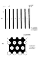
電子放出部もしくはその周辺部を微粒子膜から形成する表面伝導型放出素子の代表的な構成には、平面型と垂直型の2種類があげられる。
【0055】
(平面型の表面伝導型放出素子)
まず最初に、本実施の形態の平面型の表面伝導型放出素子の素子構成と製法について説明する。図6に示すのは、平面型の表面伝導型放出素子の構成を説明するための平面図(a)および断面図(b)である。図中、1101は基板、1102と1103は素子電極、1104は導電性薄膜、1105は通電フォーミング処理により形成した電子放出部、1113は通電活性化処理により形成した薄膜である。基板1101としては、例えば、石英ガラスや青板ガラスをはじめとする各種ガラス基板や、アルミナをはじめとする各種セラミクス基板、あるいは上述の各種基板上に例えばSiO2を材料とする絶縁層を積層した基板、などを用いることができる。
【0056】
また、基板1101上に基板面と平行に対向して設けられた素子電極1102,1103は、導電性を有する材料によって形成されている。例えば、Ni,Cr,Au,Mo,W,Pt,Ti,Cu,Pd,Ag等をはじめとする金属、或はこれらの金属の合金、或はIn2O3−SnO2をはじめとする金属酸化物、ポリシリコンなどの半導体、などの中から適宜材料を選択して用いればよい。電極を形成するには、例えば真空蒸着などの製膜技術とフォトリソグラフィー、エッチングなどのパターニング技術を組み合わせて用いれば容易に形成できるが、それ以外の方法(例えば印刷技術)を用いて形成しても差し支えない。
【0057】
これら素子電極1102,1103の形状は、この電子放出素子の応用目的に合わせて適宜設計される。一般的には、電極間隔Lは通常は数百オングストロームから数百μmの範囲から適当な数値を選んで設計されるが、なかでも、本実施の形態の表示装置に応用するために好ましいのは数μmより数十μmの範囲である。また、素子電極の厚さdについては、通常は数百オングストロームから数μmの範囲から適当な数値が選ばれる。
【0058】
また、導電性薄膜1104の部分には、微粒子膜を用いる。ここで述べた微粒子膜とは、構成要素として多数の微粒子を含んだ膜(島状の集合体も含む)のことをさす。微粒子膜を微視的に調べれば、通常は、個々の微粒子が離間して配置された構造か、あるいは微粒子が互いに隣接した構造か、あるいは微粒子が互いに重なり合った構造が観測される。
【0059】
微粒子膜に用いた微粒子の粒径は、数オングストロームから数千オングストロームの範囲に含まれるものであるが、中でも好ましいのは10オングストロームから200オングストロームの範囲のものである。また、微粒子膜の膜厚は、以下に述べるような諸条件を考慮して適宜設定される。すなわち、素子電極1102あるいは1103と電気的に良好に接続するのに必要な条件、後述する通電フォーミングを良好に行うのに必要な条件、微粒子膜自身の電気抵抗を後述する適宜の値にするために必要な条件、などである。
【0060】
具体的には、数オングストロームから数千オングストロームの範囲のなかで設定するが、中でも好ましいのは10オングストロームから500オングストロームの間である。
【0061】
また、微粒子膜を形成するのに用いられうる材料としては、例えば、Pd,Pt,Ru,Ag,Au,Ti,In,Cu,Cr,Fe,Zn,Sn,Ta,W,Pb,などをはじめとする金属や、PdO,SnO2,In2O3,PbO,Sb2O3,などをはじめとする酸化物や、HfB2,ZrB2,LaB6,CeB6,YB4,GdB4,などをはじめとする硼化物や、TiC,ZrC,HfC,TaC,SiC,WC,などをはじめとする炭化物や、TiN,ZrN,HfN,などをはじめとする窒化物や、Si,Ge,などをはじめとする半導体や、カーボン、などがあげられ、これらの中から適宜選択される。
【0062】
以上述べたように、導電性薄膜1104を微粒子膜で形成したが、そのシート抵抗値については、10の3乗から10の7乗[オーム/□]の範囲に含まれるよう設定した。
【0063】
なお、導電性薄膜1104と素子電極1102および1103とは、電気的に良好に接続されるのが望ましいため、互いの一部が重なりあうような構造をとっている。その重なり方は、図6の例においては、下から、基板、素子電極、導電性薄膜の順序で積層したが、場合によっては下から基板、導電性薄膜、素子電極、の順序で積層しても差し支えない。
【0064】
また、電子放出部1105は、導電性薄膜1104の一部に形成された亀裂状の部分であり、電気的には周囲の導電性薄膜よりも高抵抗な性質を有している。亀裂は、導電性薄膜1104に対して、後述する通電フォーミングの処理を行うことにより形成する。亀裂内には、数オングストロームから数百オングストロームの粒径の微粒子を配置する場合がある。なお、実際の電子放出部の位置や形状を精密かつ正確に図示するのは困難なため、図6においては模式的に示した。
【0065】
また、薄膜1113は、炭素もしくは炭素化合物よりなる薄膜で、電子放出部1105およびその近傍を被覆している。薄膜1113は、通電フォーミング処理後に、後述する通電活性化の処理を行うことにより形成する。
【0066】
この薄膜1113は、単結晶グラファイト、多結晶グラファイト、非晶質カーボン、のいずれかか、もしくはその混合物であり、膜厚は500[オングストローム]以下とするが、300[オングストローム]以下とするのがさらに好ましい。なお、実際の薄膜1113の位置や形状を精密に図示するのは困難なため、図6においては模式的に示した。また、平面図(a)においては、薄膜1113の一部を除去した素子を図示した。
【0067】
以上、好ましい素子の基本構成を述べたが、本実施の形態においては以下のような素子を用いた。
【0068】
即ち、基板1101には青板ガラスを用い、素子電極1102と1103にはNi薄膜を用いた。素子電極の厚さdは1000[オングストローム]、電極間隔Lは2[μm]とした。微粒子膜の主要材料としてPdもしくはPdOを用い、微粒子膜の厚さは約100[オングストローム]、幅Wは100[μm]とした。
【0069】
次に、好適な平面型の表面伝導型放出素子の製造方法について説明する。図7(a)〜(d)は、表面伝導型放出素子の製造工程を説明するための断面図で、各部材の表記は前記図6と同一である。
【0070】
(1)まず、図7(a)に示すように、基板1101上に素子電極1102および1103を形成する。これら素子電極1102,1103を形成するにあたっては、予め基板1101を洗剤、純水、有機溶剤を用いて十分に洗浄した後、素子電極1102,1103の材料を堆積させる(堆積する方法としては、例えば、蒸着法やスパッタ法などの真空成膜技術を用ればよい)。その後、堆積した電極材料を、フォトリソグラフィー・エッチング技術を用いてパターニングし、(a)に示した一対の素子電極(1102と1103)を形成する。
【0071】
(2)次に、同図(b)に示すように導電性薄膜1104を形成する。
【0072】
この導電性薄膜1104を形成するにあたっては、まず前記(a)の基板1101に有機金属溶液を塗布して乾燥し、加熱焼成処理して微粒子膜を成膜した後、フォトリソグラフィー・エッチングにより所定の形状にパターニングする。ここで、有機金属溶液とは、導電性薄膜1104に用いる微粒子の材料を主要元素とする有機金属化合物の溶液である(具体的には、本実施の形態では、主要元素としてPdを用いた。また、この実施の形態では塗布方法として、ディッピング法を用いたが、それ以外の例えばスピンナー法やスプレ法を用いてもよい)。
【0073】
また、この微粒子膜で作られる導電性薄膜の成膜方法としては、本実施の形態で用いた有機金属溶液の塗布による方法以外の、例えば真空蒸着法やスパッタ法、あるいは化学的気相堆積法などを用いる場合もある。
【0074】
(3)次に、同図(c)に示すように、フォーミング用電源1110から素子電極1102と1103の間に適宜の電圧を印加し、通電フォーミング処理を行って、電子放出部1105を形成する。この通電フォーミング処理とは、微粒子膜で作られた導電性薄膜1104に通電を行って、その一部を適宜に破壊、変形、もしくは変質せしめ、電子放出を行うのに好適な構造に変化させる処理のことである。この微粒子膜で作られた導電性薄膜1104のうち電子放出を行うのに好適な構造に変化した部分(即ち、電子放出部1105)においては、薄膜1104に適当な亀裂が形成されている。なお、この導電性薄膜1104を電子放出部1105が形成される前と比較すると、その電子放出部1105が形成された後では、素子電極1102と1103の間で計測される電気抵抗は大幅に増加する。
【0075】
この通電フォーミング時の通電方法をより詳しく説明するために、図8に、フォーミング用電源1110から印加する適宜の電圧波形の一例を示す。微粒子膜で作られた導電性薄膜1104をフォーミングする場合には、パルス状の電圧が好ましく、本実施の形態の場合には、同図に示したようにパルス幅T1の三角波パルスをパルス間隔T2で連続的に印加した。その際には、三角波パルスの波高値Vpfを、順次昇圧した。また、電子放出部1105の形成状況をモニタするためのモニタパルスPmを適宜の間隔で三角波パルスの間に挿入し、その際に流れる電流を電流計1111(図7)で計測した。
【0076】
本実施の形態においては、例えば10のマイナス5乗[torr]程度の真空雰囲気下において、例えばパルス幅T1を1[ミリ秒]、パルス間隔T2を10[ミリ秒]とし、波高値Vpfを1パルスごとに0.1[V]ずつ昇圧した。そして、三角波を5パルス印加する度に1回の割りで、モニタパルスPmを挿入した。ここでフォーミング処理に悪影響を及ぼすことがないように、モニタパルスの電圧Vpmは0.1[V]に設定した。そして、素子電極1102と1103の間の電気抵抗が1×10の6乗[オーム]になった段階、即ち、モニタパルスPm印加時に電流計1111で計測される電流が1×10のマイナス7乗[A]以下になった段階で、フォーミング処理にかかわる通電を終了した。
【0077】
なお、上記の方法は、本実施の形態の表面伝導型放出素子に関する好ましい方法であり、例えば微粒子膜の材料や膜厚、あるいは素子電極間隔Lなど表面伝導型放出素子の設計を変更した場合には、それに応じて通電の条件を適宜変更するのが望ましい。
【0078】
(4)次に、図7(d)に示すように、活性化用電源1112から素子電極1102と1103の間に適宜の電圧を印加し、通電活性化処理を行って、電子放出特性の改善を行う。この通電活性化処理とは、通電フォーミング処理により形成された電子放出部1105に適宜の条件で通電を行って、その近傍に炭素もしくは炭素化合物を堆積せしめる処理のことである。(図においては、炭素もしくは炭素化合物よりなる堆積物を部材1113として模式的に示した)。尚、このような通電活性化処理を行うことにより、行う前と比較して、同じ印加電圧における放出電流を典型的には100倍以上に増加させることができる。
【0079】
具体的には、10のマイナス4乗ないし10のマイナス5乗[torr]の範囲内の真空雰囲気中で、電圧パルスを定期的に印加することにより、真空雰囲気中に存在する有機化合物を起源とする炭素もしくは炭素化合物を堆積させる。堆積物1113は、単結晶グラファイト、多結晶グラファイト、非晶質カーボン、のいずれかか、もしくはその混合物であり、膜厚は500[オングストローム]以下、より好ましくは300[オングストローム]以下である。
【0080】
通電方法をより詳しく説明するために、図9(a)に、活性化用電源1112から印加する適宜の電圧波形の一例を示す。本実施の形態においては、一定電圧の矩形波を定期的に印加して通電活性化処理を行ったが、具体的には,矩形波の電圧Vacは14[V],パルス幅T3は1[ミリ秒],パルス間隔T4は10[ミリ秒]とした。なお、上述の通電条件は、本実施の形態の表面伝導型放出素子に関する好ましい条件であり、表面伝導型放出素子の設計を変更した場合には、それに応じて条件を適宜変更するのが望ましい。
【0081】
図7(d)に示す1114は、表面伝導型放出素子から放出される放出電流Ieを捕捉するためのアノード電極で、直流高電圧電源1115および電流計1116が接続されている(なお、基板1101を、表示パネルの中に組み込んでから活性化処理を行う場合には、表示パネルの蛍光面をアノード電極1114として用いる)。活性化用電源1112から電圧を印加する間、電流計1116で放出電流Ieを計測して通電活性化処理の進行状況をモニタし、活性化用電源1112の動作を制御する。電流計1116で計測された放出電流Ieの一例を図9(b)に示すが、活性化電源1112からパルス電圧を印加しはじめると、時間の経過とともに放出電流Ieは増加するが、やがて飽和してほとんど増加しなくなる。このように、放出電流Ieがほぼ飽和した時点で活性化用電源1112からの電圧印加を停止し、通電活性化処理を終了する。
【0082】
なお、上述の通電条件は、本実施の形態の表面伝導型放出素子に関する好ましい条件であり、表面伝導型放出素子の設計を変更した場合には、それに応じて条件を適宜変更するのが望ましい。
【0083】
以上のようにして、図7(e)に示す平面型の表面伝導型放出素子を製造した。
【0084】
(垂直型の表面伝導型放出素子)
次に、電子放出部もしくはその周辺を微粒子膜から形成した表面伝導型放出素子のもうひとつの代表的な構成、すなわち垂直型の表面伝導型放出素子の構成について説明する。
【0085】
図10は、本実施の形態の垂直型表面伝導型放出素子の基本構成を説明するための模式的な断面図であり、図中の1201は基板、1202と1203は素子電極、1206は段差形成部材、1204は微粒子膜を用いた導電性薄膜、1205は通電フォーミング処理により形成した電子放出部、1213は通電活性化処理により形成した薄膜、である。
【0086】
垂直型が先に説明した平面型と異なる点は、素子電極のうちの片方(1202)が段差形成部材1206上に設けられており、導電性薄膜1204が段差形成部材1206の側面を被覆している点にある。従って、図6の平面型における素子電極間隔Lは、垂直型においては段差形成部材1206の段差高Lsとして設定される。なお、基板1201、素子電極1202および1203、微粒子膜を用いた導電性薄膜1204、については、前記平面型の説明中に列挙した材料を同様に用いることが可能である。また、段差形成部材1206には、例えばSiO2 のような電気的に絶縁性の材料を用いる。
【0087】
次に、垂直型の表面伝導型放出素子の製法について説明する。図11(a)〜(f)は、製造工程を説明するための断面図で、各部材の表記は前記図106と同一である。
【0088】
(1)まず、図11(a)に示すように、基板1201上に素子電極1203を形成する。
【0089】
(2)次に、同図(b)に示すように、段差形成部材を形成するための絶縁層を積層する。絶縁層は、例えばSiO2をスパッタ法で積層すればよいが、例えば真空蒸着法や印刷法などの他の成膜方法を用いてもよい。
【0090】
(3)次に、同図(c)に示すように、絶縁層の上に素子電極1202を形成する。
【0091】
(4)次に、同図(d)に示すように、絶縁層の一部を、例えばエッチング法を用いて除去し、素子電極1203を露出させる。
【0092】
(5)次に、同図(e)に示すように、微粒子膜を用いた導電性薄膜1204を形成する。形成するには、前記平面型の場合と同じく、例えば塗布法などの成膜技術を用いればよい。
【0093】
(6)次に、前記平面型の場合と同じく、通電フォーミング処理を行い、電子放出部を形成する。(図7(c)を用いて説明した平面型の通電フォーミング処理と同様の処理を行えばよい。)
(7)次に、前記平面型の場合と同じく、通電活性化処理を行い、電子放出部近傍に炭素もしくは炭素化合物を堆積させる。(図7(d)を用いて説明した平面型の通電活性化処理と同様の処理を行えばよい。)
以上のようにして、図11(f)に示す垂直型の表面伝導型放出素子を製造した。
【0094】
(表示装置に用いた表面伝導型放出素子の特性)
以上、平面型と垂直型の表面伝導型放出素子について素子構成と製法を説明したが、次に表示装置に用いた素子の特性について述べる。
【0095】
図12に、表示装置に用いた素子の、(放出電流Ie)対(素子印加電圧Vf)特性、および(素子電流If)対(素子印加電圧Vf)特性の典型的な例を示す。なお、放出電流Ieは素子電流Ifに比べて著しく小さく、同一尺度で図示するのが困難であるうえ、これらの特性は素子の大きさや形状等の設計パラメータを変更することにより変化するものであるため、2本のグラフは各々任意単位で図示した。
【0096】
本実施の形態の表示装置に用いた素子は、放出電流Ieに関して以下に述べる3つの特性を有している。
【0097】
第1に、ある電圧(これを閾値電圧Vthと呼ぶ)以上の大きさの電圧を素子に印加すると急激に放出電流Ieが増加するが、一方、閾値電圧Vth未満の電圧では放出電流Ieはほとんど検出されない。すなわち、放出電流Ieに関して、明確な閾値電圧Vthを持った非線形素子である。
【0098】
第2に、放出電流Ieは素子に印加する電圧Vfに依存して変化するため、電圧Vfで放出電流Ieの大きさを制御できる。
【0099】
第3に、素子に印加する電圧Vfに対して素子から放出される電流Ieの応答速度が速いため、電圧Vfを印加する時間の長さによって素子から放出される電子の電荷量を制御できる。
【0100】
以上のような特性を有するため、表面伝導型放出素子を表示装置に好適に用いることができた。例えば多数の素子を表示画面の画素に対応して設けた表示装置において、第1の特性を利用すれば、表示画面を順次走査して表示を行うことが可能である。即ち、駆動中の素子には所望の発光輝度に応じて閾値電圧Vth以上の電圧を適宜印加し、非選択状態の素子には閾値電圧Vth未満の電圧を印加する。こうして駆動する素子を順次切り替えてゆくことにより、表示画面を順次走査して表示を行うことが可能である。
【0101】
また、第2の特性か又は第3の特性を利用することにより、発光輝度を制御することができるため、階調表示を行うことが可能である。
【0102】
(多数素子を単純マトリクス配線したマルチ電子源の構造)
上述の表面伝導型放出素子を基板上に配列して単純マトリクス配線したマルチ電子源の構造は前述の図3及び図4に示す通りである。
【0103】
(マルチ電子源の駆動回路の構成(および駆動方法))
図13は、NTSC方式のテレビ信号に基づいてテレビジョン表示を行うための駆動回路の概略構成をブロック図で示したものである。同図中、表示パネル1701は前述した表示パネルに相当するもので、前述した様に製造され動作する。また、走査回路1702は表示ラインを走査し、制御回路1703は走査回路1702に入力する信号等を生成する。シフトレジスタ1704は1ライン毎のデータをシフトして保持し、ラインメモリ1705は、シフトレジスタ1704からの1ライン分のデータを受取って保持した後、変調信号発生器1707に出力する。同期信号分離回路1706はNTSC信号から同期信号を分離する。1710は制御部で、テーブル1711に記憶されているスペーサ近傍の素子、及びそれら素子への印加電圧(素子電圧)を基に、変調信号発生器1707における変調信号の振幅を制御して、それらの素子に印加される素子電圧を制御することにより、後述するスペーサ近傍の画像の輝度のバラツキを抑えている。この処理は図15以降を参照して詳しく後述する。
【0104】
以下、図13の装置各部の機能を詳しく説明する。
【0105】
まず表示パネル1701は、端子Dx1ないしDxMおよび端子Dy1ないしDyN、および高圧端子Hvを介して外部の電気回路と接続されている。このうち、端子Dx1ないしDxMには、表示パネル1701内に設けられているマルチ電子源、すなわちM行N列の行列状にマトリクス配線された冷陰極素子を1行(N素子)ずつ順次駆動してゆくための走査信号が印加される。一方、端子Dy1ないしDyNには、前記走査信号により選択された1行分のN個の各素子の出力電子ビームを制御するための変調信号が印加される。また、高圧端子Hvには、直流電圧源Vaより、例えば5[kV]の直流電圧が供給されるが、これはマルチ電子源より出力される電子ビームに蛍光体を励起するのに十分なエネルギーを付与するための加速電圧である。
【0106】
次に、走査回路1702について説明する。この回路1702は、内部にM個のスイッチング素子(図中、S1ないしSMで模式的に示されている)を備えるもので、各スイッチング素子は、直流電圧源Vxの出力電圧もしくは0[V](グランドレベル)のいずれか一方を選択し、表示パネル1701の端子Dx1ないしDxMと電気的に接続するものである。S1ないしSMの各スイッチング素子は、制御回路1703が出力する制御信号TSCANに基づいて動作するが、実際には例えばFETのようなスイッチング素子を組合わせる事により容易に構成することが可能である。なお、前記直流電圧源Vxは、図12に例示した電子放出素子の特性に基づき、走査されていない素子に印加される駆動電圧が電子放出閾値電圧Vth電圧以下となるよう、一定電圧を出力するよう設定されている。
【0107】
また、制御回路1703は、外部より入力する画像信号に基づいて適切な表示が行なわれるように各部の動作を整合させる働きをもつものである。次に説明する同期信号分離回路1706より送られる同期信号TSYNCに基づいて、各部に対してTSCANおよびTSFTおよびTMRYの各制御信号を発生する。同期信号分離回路1706は、外部から入力されるNTSC方式のテレビ信号から、同期信号成分と輝度信号成分とを分離するための回路で、良く知られているように周波数分離(フィルタ)回路を用いれば容易に構成できるものである。同期信号分離回路1706により分離された同期信号は、良く知られるように垂直同期信号と水平同期信号より成るが、ここでは説明の便宜上、TSYNC信号として図示した。一方、前記テレビ信号から分離された画像の輝度信号成分を便宜上DATA信号と表すが、同信号はシフトレジスタ1704に入力される。
【0108】
シフトレジスタ1704は、時系列的にシリアルに入力される前記DATA信号を、画像の1ライン毎にシリアル/パラレル変換するためのもので、前記制御回路1703より送られる制御信号TSFTに基づいて動作する。すなわち、制御信号TSFTシフトレジスタ1704のシフトクロックであると言い換えることもできる。シリアル/パラレル変換された画像1ライン分(電子放出素子n素子分の駆動データに相当する)のデータは、Id1ないしIdNのN個の信号として前記シフトレジスタ1704より出力される。
【0109】
ラインメモリ1705は、画像1ライン分のデータを必要時間の間だけ記憶するための記憶装置であり、制御回路1703より送られる制御信号TMRYにしたがって適宜Id1ないしIdNの内容を記憶する。記憶された内容は、I'd1ないしI'dNとして出力され、変調信号発生器1707に入力される。
【0110】
変調信号発生器1707は、前記画像データI'd1ないしI'dNの各々と、制御部1710からの指示に応じて、電子放出素子1015の各々を適切に駆動変調するための信号源で、その出力信号は、端子Dy1ないしDyNを通じて表示パネル1701内の電子放出素子1015に印加される。尚、この駆動制御は図16を参照して詳しく後述する。
【0111】
図12を用いて説明したように、本発明の実施の形態に係わる表面伝導型放出素子は放出電流Ieに対して以下の基本特性を有している。すなわち、電子放出には明確な閾値電圧Vth(後述する実施の形態の表面伝導型放出素子では8[V])があり、閾値Vth以上の電圧を印加された時のみ電子放出が生じる。また、電子放出閾値Vth以上の電圧に対しては、図12のグラフのように、電圧の変化に応じて放出電流Ieも変化する。このことから、本実施の形態の素子にパルス状の電圧を印加する場合、例えば電子放出閾値Vth以下の電圧を印加しても電子放出は生じないが、電子放出閾値Vth以上の電圧を印加する場合には表面伝導型放出素子から電子ビームが出力される。その際、パルスの波高値Vmを変化させることにより出力電子ビームの強度を制御することが可能である。また、パルスの幅Pwを変化させることにより出力される電子ビームの電荷の総量を制御することが可能である。
【0112】
従って、入力信号に応じて、電子放出素子を変調する方式としては、電圧変調方式、パルス幅変調方式等が採用できる。電圧変調方式を実施するに際しては、変調信号発生器1707として、一定長さの電圧パルスを発生し、入力されるデータに応じて適宜パルスの波高値を変調するような電圧変調方式の回路を用いることができる。また、パルス幅変調方式を実施するに際しては、変調信号発生器1707として、一定の波高値の電圧パルスを発生し、入力されるデータに応じて適宜電圧パルスの幅を変調するようなパルス幅変調方式の回路を用いることができる。
【0113】
シフトレジスタ1704やラインメモリ1705は、デジタル信号式のものでもアナログ信号式のものでも採用できる。すなわち、画像信号のシリアル/パラレル変換や記憶が所定の速度で行われればよいからである。
【0114】
デジタル信号式を用いる場合には、同期信号分離回路1706の出力信号DATAをデジタル信号化する必要があるが、これには同期信号分離回路1706の出力部にA/D変換器を設ければよい。これに関してラインメモリ115の出力信号がデジタル信号かアナログ信号かにより、変調信号発生器に用いられる回路が若干異なったものとなる。すなわち、デジタル信号を用いた電圧変調方式の場合、変調信号発生器1707には、例えばD/A変換回路を用い、必要に応じて増幅回路などを付加する。パルス幅変調方式の場合、変調信号発生器1707には、例えば高速の発振器および発振器の出力する波数を計数する計数器(カウンタ)および計数器の出力値と前記メモリの出力値を比較する比較器(コンパレータ9を組み合わせた回路を用いる。必要に応じて、比較器の出力するパルス幅変調された変調信号を電子放出素子の駆動電圧にまで電圧増幅するための増幅器を付与することもできる。
【0115】
アナログ信号を用いた電圧変調方式の場合、変調信号発生器1707には、例えばオペアンプなどを用いた増幅回路を採用でき、必要に応じてシフトレベル回路などを付加することもできる。パルス幅変調方式の場合には、例えば、電圧制御型発信回路(VCO)を採用でき、必要に応じて電子放出素子の駆動電圧まで電圧増幅するための増幅器を付加することもできる。
【0116】
このような構成をとりうる本発明の適用可能な画像表示装置においては、各電子放出素子に、容器外端子Dx1乃至DxM、Dy1乃至DyNを介して電圧を印加することにより、電子放出が生じる。高圧端子Hvを介してメタルバック1019あるいは透明電極(不図示)に高圧を印加し、電子ビームを加速する。加速された電子は蛍光膜1018に衝突し、発光が生じて画像が形成される。
【0117】
ここで述べた画像表示装置の構成は、本発明の実施の形態に適用可能な画像形成装置の一例であり、本発明の思想に基づいて種々の変形が可能である。入力信号についてはNTSC方式を挙げたが、入力信号はこれに限るものではなく、PAL、SECAM方式など他、これらより多数の走査線からなるTV信号(MUSE方式をはじめとする高品位TV)方式をも採用できる。
【0118】
次に、本実施の形態の特徴である電子源からの電子ビームの軌道を制御して、スペーサ近傍での画像劣化を防止する構成について説明する。
【0119】
<電子源の駆動電圧とスペーサ位置によるビームずれの関係>
本実施の形態では、スペーサ4020と表面伝導型放出素子との位置関係に応じて、その電子放出素子の駆動電圧(素子電圧)を調整することによって、スペーサ4020の帯電に起因する画像の歪みを防止している。
【0120】
この実施の形態の動作を詳しく説明する前に、まず、素子電圧Vfとその素子から放出される電子の軌道との関係について説明する。
【0121】
まず図14を参照して、表面伝導型放出素子から放出された電子の軌道と素子電圧Vfの関係について説明する。
【0122】
(放出電子の軌道と素子電圧Vfの関係)
図14は、図2に示された表示パネルの断面を示しており、電子放出素子1012から放出された電子がフェースプレート1107の蛍光膜1018に衝突する状態を説明する図である。
【0123】
フェースプレート1017の内側には蛍光体(膜)1018が塗布されている。図4を参照して前述したように、素子電極1102,1103はそれぞれ列方向配線1014(図2)、行方向1013(図2)に接続されており、これら素子電極1102,1103間に所定値以上の素子電圧(例えばV(f))が印加されると、この電子放出素子1012の電子放出部1105から電子が放出される。こうして放出された電子は、フェースプレート1107と電子放出部1105との間に印加されたアノード電圧(加速電圧)Va[V]によりフェースプレート1017方向に加速されてフェースプレート1017に照射される。この時、放出された電子は中心軸500に沿って電子放出部1105の真上に進むのではなく、図14の電子軌道501に沿って進む。この電子軌道501は、素子電極1102が正極性、電極1103が負極性となるよう素子電圧Vfを印加したときの状態を示すものである。この場合、中心軸500と蛍光膜1018上での電子のランディング位置との距離Lefは次式(1)により算出できる。
【0124】
Lef=2×K×Lh×SQRT(Vf/Va)
ただし、Lh[m]は、放出素子1012と蛍光体1018との間の距離
K[m]は、放出素子1012の種類や形状により決まる定数
また、SQRT(A)は、Aの平方根を示す。
【0125】
図15(A)(B)は図2に示された表示パネルにおける放出素子1012と蛍光体1018との位置関係を説明する図である。
【0126】
図15(A)は、図2の表示パネルのi行目に対して素子電圧Vf1を印加した場合、図15(B)はi行目に対して素子電圧Vf2を印加した場合について、それぞれY軸座標方向に垂直な平面で切った断面図を示し、放出素子1012と蛍光体1018以外は省略して描いてある。
【0127】
図15(A)に示すように、素子電圧Vf1で駆動を行った場合の、i行目の放出素子1012の電子放出部1105の中心から蛍光体1018へのランディング位置までのX方向のずれはPX1で表され、図15(B)の素子電圧Vf2を印加した場合のi行目の放出素子1012の電子放出部1105の中心から蛍光体1018へのランディング位置までのX方向のずれがPX2で示されている。但しここで放出素子1012の印加電圧Vf2はVf1よりも大きいものとする。
【0128】
図15(B)に示すように、放出素子1012に印加する素子電圧をVf2(>Vf1)と高くすることにより、放出された電子の軌道をより正極の電位が印加されている素子電極(1102)側に曲げることができ、これにより電子の蛍光体1018上のランディング位置までのずれPX2(>PX1)を大きくすることができる。このようにして、各放出素子ごとに、それに印加する素子電圧を変えることによって、マトリクス状に配置された各放出素子より放出される電子を所望の位置に照射して所望の表示を行うことができる。
【0129】
また、図14に示すように電極1103が負極性、電極1102が正極性となるよう素子電圧Vfを印加することにより、電子軌道の制御の自由度を上げることができ、さらに好適に電子を所望の位置に照射して所望の表示を行うことができる。
【0130】
以上のように素子電圧を変えることによって、その素子から放出される電子の軌道を変えることができることがわかる。この特性を利用して、スペーサ4020の帯電の影響を補正する実施の形態を以下で説明する。
【0131】
(スペーサと放出電子の軌道)
前述のように、負の電位を有する電子が衝突する事によりスペーサ4020は正に帯電されるため、各素子より放出される電子の内スペーサ4020の近傍の電子はスペーサ4020側に吸引され、その電子軌道が曲げられる。このことを図16(A)〜(C)を参照して説明する。
【0132】
図16(A)はスペーサ4020がない場合の図2に示された表示パネルにおける放出素子1012と蛍光体1018との位置関係を示す図である。
【0133】
図16(B)(C)は、図2に示された表示パネルにおける放出素子1012と蛍光体1018およびスペーサ4020との位置関係を説明する図である。
【0134】
図16(A)に示すように、スペーサ4020がない場合もしくはスペーサから充分遠い場合は、各素子1012から放出される電子は、それに印加されている素子電圧Vfに応じて一意に決まる距離PX3だけずれた位置に到達する。このときの素子電圧をVf3とする。
【0135】
しかし、素子電圧をVf3に一定としても、図16(B)に示すように、スペーサ4020周辺の素子1012が駆動された場合、それから放出された電子のランディング位置のずれ(距離)が異なってくる。
【0136】
即ち、素子1012−1のように、放出された電子の方向がスペーサ4020に向かう方向の素子が駆動された場合は、その電子軌道は大きくスペーサ4020の方向に移動し、その電子のランディング位置は距離PX4(>PX3)もずれることになる。また、素子1012−2のように、電子の放出方向がスペーサ4020から遠ざかる方向の場合は、その電子の軌道はスペーサ4020の方向に傾斜し、そのランディング位置は距離PX5(<PX3)だけずれることになる。
【0137】
この電子軌道は、前述の式(1)で示されるように、素子電圧Vfを調節することにより、電子が到達するランディング位置(距離)を調節することができる。
【0138】
図16(C)は、スペーサ4020の帯電による影響を補正するために、そのスペーサ4020近傍の放出素子に印加する素子電圧Vfを調整し、蛍光体1018上へのランディング位置(距離)を一定とした場合を示している。
【0139】
ここでは、電子放出素子1012−3の素子電圧をVf4(<Vf3)とし、また、放出素子1012−4の素子電圧をVf5(>Vf3)とする。こうして、スペーサ4020の帯電量に見合った素子電圧を、そのスペーサ4020近傍の放出素子に印加することにより、蛍光体1018上にランディングする位置までの距離PX6を、図16(A)のように、スペーサ4020から十分遠い素子1012の場合の距離PX3と略同じにすることができる。
【0140】
図17は、図16のようにスペーサに対する放出素子の位置により、その素子電圧を変更して電子軌道を制御する方法を示すフローチャートである。
【0141】
まずステップS1で、スペーサ4020の帯電量を調べる。これは図示しない帯電測定器などにより各スペーサの帯電量を測定しても良く、また或はこの表示パネルの動作時間等に応じて、その帯電量を予測して求めても良い。次にステップS2に進み、ステップS1で求めた帯電量が所定量以上であるかどうかを調べ、所定量以下であれば、電子の軌道に対する影響が少ないものとして、特に補正処理を行うことなく処理を終了する。ステップS2で、その帯電量が所定量以上の時はステップS3に進み、駆動する素子がスペーサ4020から所定の範囲(距離)内にある素子で、その素子から放出された電子の方向にスペーサ4020があるかどうかを調べ、そうであればその素子の素子電圧を、例えば図16の例ではVf4(<Vf3)とする。尚、ここで所定の範囲とは、スペーサ4020の帯電により、その素子から放出された電子の軌道が影響を受ける素子までの距離に相当している。次にステップS4に進み、駆動する素子がスペーサ4020から所定の範囲(距離)内にある素子で、その素子から放出された電子の方向と反対方向にスペーサ4020があるかどうかを調べ、そうであればその素子の素子電圧を、例えば図16の例ではVf5(>Vf3)とする。そしてそれ以外の素子には、素子電圧Vf3を印加する。これにより、図16の(A)及び(C)で示すように、スペーサ4020近傍の素子と、それ以外の素子とから放出された電子のずれ距離が略一定になる。
【0142】
(スペーサ4020位置と素子の電子放出方向の配置)
以上の例では、スペーサ4020の帯電による影響を補正するために、素子電圧の大きさを適宜調節する方法について述べてきた。しかし、このような素子電圧の調節による電子軌道の制御は、電子放出方向(図2の例では行方向配線1013方向)のみに有効であるため、この方法を好適に実施するためには、スペーサ4020の位置と放出素子の電子放出方向の関係を調節することが必要となる。
【0143】
そこで次に、スペーサ4020の位置と放出素子の電子放出方向との関係について本実施の形態の画像表示装置の構成を図18を参照して説明する。
【0144】
本実施の形態の画像表示装置において、スペーサ4020と素子1012との配置の以外の基本的な構成は、図2で示した表示パネル構成と同様である。
【0145】
図18は、スペーサ4020と電子放出素子の配置関係を示す画像形成装置の平面図である。
【0146】
基板1011上には、前述の図6で示すものと同様な表面伝導型放出素子1012が配列され、これらの素子1012は行方向配線1013と列方向配線1014により単純なマトリクス状に配線されている。行方向配線1013と列方向配線1014の交差する部分には、電極間に絶縁層(不図示)が形成されており、電気的な絶縁が保たれている。ここで図18のように、スペーサ4020をX軸(行方向配線)上に配設した場合は、素子1012の電子放出方向がy軸と平行になるように形成する。
【0147】
このようにX軸上にスペーサ4020を設けた場合、スペーサ4020が正に帯電することによる電界720はY軸と平行となり、スペーサ4020近傍での電子軌道はスペーサ4020に近づく方向へ変位する。つまり、スペーサ4020近傍での電子軌道は、Y軸に平行に変位する。
【0148】
このスペーサ4020の帯電による電子軌道の変化を防止するためには、素子1012からの放出電子方向をY軸と平行とし、素子電圧Vfを適宜調節することにより、最も有効に電子軌道を調節して蛍光体1018へのランディング位置を制御することができる。
【0149】
また、スペーサ4020をY軸上に形成し、放出素子から放出される電子方向をX軸と平行にした場合も同様に、蛍光体1018へのランディング位置を一定とすることができる。
【0150】
つまり本実施の形態では、スペーサ4020の帯電により生じる電界の方向と各素子から放出される電子の方向とが平行となるようにし、各電子放出素子に対する印加電圧Vfを、スペーサ4020に対する位置に応じて適宜変更することにより、スペーサ4020近傍での電子軌道のずれに起因するスペーサ4020近傍での画像の歪みを防止することができる。
【0151】
<メモリ機能を利用した調整方法の説明>
上述したように、スペーサ4020の帯電による電子軌道への影響を補正し、放出素子から放出された電子を所望の蛍光体へ衝突させることが可能であることを示した。しかし、上述の実施の形態では素子毎に素子電圧を変える必要があるため、制御が複雑で各画素の輝度がばらついてしまう虞がある。
【0152】
これについて詳述する。前述の図12で述べたように、表面伝導型放出素子は電子放出に関して明確な閾値電圧(Vth)を有しており、Vth以上の電圧を印加することで、図12のような電子放出特性を有している。従って、Vth以上の電圧値において、素子印加電圧Vfを変化させると、それに伴って放出電流Ieも変化してしまう。この放出電流Ieの変化は輝度の変化となってしまうため、素子毎に印加電圧Vfを変化させると、その素子に応じた発光部(蛍光体部)毎に輝度がばらついてしまうという問題が発生する虞がある。
【0153】
そこで、この実施形態では、表面伝導型電子放出素子が有しているメモリ機能(素子電極に加された最大電圧値に応じた電子放出特性を有する)によって、スペーサ4020の周辺の電子放出素子のそれぞれに異なる電子放出特性を持たせ、各素子の印加電圧Vfの相違による輝度の変化を防止する。このメモリ機能を利用した処理をしておき、スペーサ近傍の素子に対して前述と同様の制御を行う。これにより、スペーサ4020の帯電の影響による画像の歪みおよび輝度の変化を防止することが可能となる。
【0154】
この実施の形態の動作を詳しく説明する前に、図19および図20を参照してメモリ機能について説明する。
【0155】
本願発明者らは、予めフォーミング処理並びに通電活性化処理を施した表面伝導型放出素子を有機ガスの分圧を低減した環境下で駆動して、その電気的特性を測定した。
【0156】
図19(a)(b)は、表面伝導型放出素子に印加した駆動信号の電圧波形を示すグラフ図で、横軸に時間軸を、縦軸には表面伝導型放出素子に印加した電圧(以下、素子電圧Vfと記す)を示している。
【0157】
図19(a)に示すように、駆動信号として連続した矩形電圧パルスを用い、これらの電圧パルスの印加期間を第1期間から第3期間の3つの期間に分け、各期間内においては同一の幅で同じ高さのパルスをそれぞれ100パルスずつ印加した。この電圧パルスの波形を図19(b)に拡大して示す。
【0158】
具体的な測定条件としては、その期間も駆動信号パルス幅をT5=66.8(μ秒)、パルス周期T6=16.7(m秒)とした。これは、表面伝導型放出素子を一般のテレビジョン受像機に応用する場合の標準的な駆動条件を参考にして定めたが、これ以外の条件においてもメモリ機能を測定することは可能である。なお、表面伝導型放出素子に実効的に印加される電圧パルスの立ち上がり時間Trおよび立ち下がり時間Trが100(ナノ秒)以下となるように、駆動信号源から表面伝導型放出素子までの配線路のインピーダンスを十分に低減して測定した。
【0159】
素子電圧Vfは、第1期間と第3期間ではVf=Vf1であり、第2期間ではVf=Vf2とした。これらの電圧値Vf1及びVf2はともに表面伝導型電子放出素子の電子放出閾値よりも高い電圧であって、かつVf1<Vf2を満足するように設定した。ただし、表面伝導型放出素子の形状により電子放出閾値電圧も異なるので、測定対象となる表面伝導型放出素子に合わせて適宜設定した。また、測定時の表面伝導型放出素子周辺の雰囲気については、全圧が1×10のマイナス6乗(torr)で、有機ガスの分圧は1×10のマイナス9乗(torr)とした。
【0160】
図20(a)(b)は、図19で示した駆動信号を印加した際の表面伝導型放出素子の電気的特性を示すグラフ図で、図20(a)の横軸は素子電圧Vfを示し、縦軸は表面伝導型放出素子から放出される電流(以下、放出電流Ie)の測定値を示し、図20(b)の縦軸は表面伝導型放出素子に流れる電流(以下、素子電流If)の測定値を表わしている。
【0161】
まず、図20(a)に示した(素子電圧Vf)対(放出電流Ie)特性について説明する。図19の第1期間においては、駆動パルスに応答して表面伝導型放出素子からは特性カーブIec(1)に従って放出電流が出力される。即ち、図19(b)に示す駆動パルスの立ち上がり期間Trの間は、印加電圧VfがVth1を超えると、特性カーブIec(1)に沿って放出電流Ieは急激に増加する。そして、Vf=Vf1の期間、即ち、T5の期間には、放出電流IeはIe1の大きさを保つ。そして、駆動パルスの立ち上がり期間Tfの間では、放出電流Ieは特性カーブIec(1)に沿って急激に減少する。
【0162】
次に第2期間においてVf=Vf2のパルスが印加され始めると、特性カーブはIec(1)からIec(2)に変化する。即ち、駆動パルスの立ち上がり期間Trの間は、印加電圧VfがVth2を超えると特性カーブIec(2)に沿って放出電流Ieが急激に増加する。そして、Vf=Vf2の期間、即ち、T5の期間には、放出電流IeはIe2の大きさを保つ。そして、駆動パルスの立ち下がり期間Tfの間では、放出電流Ieは特性カーブIec(2)に沿って急激に減少する。
【0163】
次に、第3期間においては、再びVf=Vf1のパルスが印加されるが、このときには放出電流は特性化カーブにIec(2)に沿って変化する。即ち、駆動パルスの立ち上がり期間Trの間は、印加電圧VfがVth2を超えると特性カーブIec(2)に沿って放出電流Ieは急激に増加する。そして、Vf=Vf1の期間、即ち、T5の期間には、放出電流IeはIe3の大きさを保つ。そして、駆動パルスの立ち下がり期間Tfの間では、放出電流Ieは特性カーブIec(2)に沿って急激に減少する。
【0164】
このように第3期間においては、第2期間における特性カーブIec(2)がメモりされているため、第1の期間と同じ素子電圧(Vf1)が印加されても、放出電流Ieは第1期間(Ie1)よりも小さな値(Ie3)となる。
【0165】
同様に(素子電圧Vf)対(素子電流If)特性に関しても図20(b)に示すように、第1期間においては特性カーブIfc(1)に沿うようになり、それに続く第3期間においては、第2期間でメモりされた特性カーブIfc(2)に沿って動作することになる。
【0166】
なお、ここでは説明の便宜上、第1〜第3期間の3つの期間だけを例示したが、むろんこの設定条件だけに限られた現象ではない。即ち、メモリ機能が付与された表面伝導型放出素子にパルス電圧を印加する場合には、それ以前に印加された電圧値よりも高い電圧値のパルスが印加されると特性がシフトし、しかもメモりされる。そしてそれ以降、さらに高い電圧値のパルスが印加されない限りその特性がメモりされ続ける。このようなメモリ機能は、例えばFE型を始めとした他の電子放出素子においては観測されておらず、表面伝導型放出素子に特有の機能であると言える。
【0167】
図21は、このようなメモリ機能を利用してスペーサ近傍の放出素子のメモリ特性を変更するための処理を示すフローチャートである。
【0168】
まずステップS10で、その素子がスペーサから所定の距離内にあるかどうかを調べ、所定の距離内になければステップS14に進む。尚、この場合の所定の距離も、前述の図17のフローチャートの場合と同様である。ステップS10で所定の距離内にある時はステップS11に進み、その素子から電子が放出される方向にスペーサがあるかどうかをみる(図16の(B)の素子1012−1の場合に相当)。そうであればステップS12に進み、その素子のメモリ特性を、例えば図20(a)のIec(1)で示す特性とする。一方、ステップS11で、その電子の放出方向にスペーサがないとき(例えば、図16(B)の素子1012−2の場合等に相当)はステップS13に進み、その素子のメモリ特性を例えば図20(a)のIec(2)で示す特性とする。そしてステップS14に進み、全ての素子に対して処理を終了したかどうかを調べ、そうでない時はステップS10に戻り、前述の処理を実行する。こうして本実施の形態の表示パネルの全ての素子に対する処理が終了すると、この処理を終了する。
【0169】
こうしてスペーサ近傍の素子の電子放出特性を変更した後、前述の図17のフローチャートを参照して説明したように、素子に印加する電圧を制御することにより、例えば図16(B)の素子1012−1は低い素子電圧でも多くの放出電流が得られるので図16(C)のように素子電圧を下げても、同じ輝度の画像を表示できる。また図16(B)の素子1012−2は、素子電圧を高めても通常の素子電圧と略同等の放出電流が得られるので、通常の素子電圧と同様の発光輝度が得られることになる。
【0170】
[実施例]
以下に、各種実施例を挙げて本発明をさらに詳述する。
【0171】
以下に述べる各実施例においては、マルチ電子源として、前述した電極間の導電性微粒子膜に電子放出部を有するタイプのN×M個(N=3072,M=1024)の表面伝導型放出素子を、M本の行方向配線とN本の列方向配線とによりマトリクス配線(図2および図3参照)したマルチ電子源を用いた。なお、スペーサは画像形成装置の耐大気圧を得るための適当な枚数を配置している。
【0172】
(実施例1)
本実施例1を、図22を参照して説明する。
【0173】
2030は蛍光体メタルバックを含むフェースプレート、2031は電子源基板を含むリアプレート、2020はスペーサ、2013は走査信号用配線、2111−1,2111−2,2111−3,2111−4は電子放出素子、2112−1,2112−2,2112−3,2112−4のそれぞれは、各素子から放出された電子の軌道を示す。まず、素子の中心間距離a、および走査信号用配線の中心間距離aをともに3000μm、フェースプレート2030の内面とリアプレート2031の内面間の距離を4mm、加速電圧Vaを4kV、列方向配線(不図示)に−8V、走査信号用配線(2013−1,2013−2,2013−3,2013−4)に+8Vを印加し、電子放出型素子2111−1,2111−2,2111−3,2111−4の素子電圧を16Vとした。ただし、スペーサ2020には絶縁性スペーサを用いた。尚、ここで各電子放出素子は、電子の放出方向がy軸と平行になるように配置している。
【0174】
図22(B)は、図22(A)で示した画像形成装置の電子放出素子の配置を示す平面図で、2014は列方向配線を示している。
【0175】
このときの各素子の電子放出部と電子のランディング位置との位置関係を調べた。電子放出素子2111−1,2111−2,2111−3,2111−4のそれぞれから電子を放出した場合、各素子の電子放出部からランディング位置までの距離はそれぞれ約360μm(=e−1)、約390μm(=e−2)、約330μm(=e−3)、約360μm(=e−4)となり、スペーサ2020近傍の電子放出素子2111−2、2111−3を駆動した場合、そのランディング位置までのずれが大きくなっていることがわかる。実際には、スペーサ2020の近傍だけ若干の輝度低下が観測が認められた。これは、スペーサ2020の帯電による電子軌道の変化に起因していると考えられる。
【0176】
そこで、前述のように、スペーサ2020近傍の素子(ここでは2111−2および2111−3)に印加する素子印加電圧(Vf)を所定値に設定する。これによって、そのスペーサ近傍の素子(2111−2および2111−3)から放出された電子のランディング位置が、通常の素子と同様のランディング位置(約360μm)となるように制御することができる。本実施例1では、前述の式(1)に基づいて、素子2111−2に印加する素子電圧Vfを13V、素子2111−3に印加する素子電圧Vfを19Vとした。
【0177】
しかし前述のように素子への印加電圧を変えることによって、電子軌道だけでなく電子放出量(Ie)も変化してしまうため、スペーサ近傍で輝度が変化してしまう。この輝度の変化に対する対策として、前述の表面伝導型素子のメモリ機能を用いて、輝度の調整を行った。具体的には素子2111−2の素子を素子電圧Vf=13Vで、他の素子(2111−1および2111−4)と同じ電子放出量となるように、また素子2111−3の素子にはVf=19Vで他の素子(2111−1および2111−4)と同じ電子放出量となるように、予めそれぞれ所定の電圧値を印加(メモリ)させておいた。この結果、どの素子においてもそれぞれ素子中心(電子放出部)からの電子のランディング位置までの距離を略同様にでき、また電子放出量も同じとすることができ、これによりスペーサ2020近傍の素子からの電子ビームずれ、及び輝度の変化のない良好な画像を得ることができた。
【0178】
(実施例2)
この実施例2が前述の実施例1と異なるのは、スペーサ2020及び電子放出素子の配置である。この実施例2を図23を参照して説明する。この実施例2では、スペーサ2020を列方向配線上に配置する。これに伴って電子放出素子の配置もx−y平面上で90度回転した方向に配置して構成し、各素子からの電子の放出方向がx軸に平行な方向となるようにした。また、各素子の中心間距離および画像配線中心間距離bを、ともに3000μmとした。
【0179】
この場合も前述の実施例1で示したものと同等に、スペーサ2020の近傍で輝度低下が見られず、歪みのない画像を得ることができた。
【0180】
(実施例3)
本実施例3は、他の実施例と異なる点はスペーサに導電性のスペーサを用いた点にある。
【0181】
本実施例3では、スペーサを絶縁性部材の表面に酸化スズの膜(以下高抵抗膜)を形成し、このスペーサが電子源およびフェースプレート(メタルバック)との間で導電性を有するフリットを介して電気的に接続されている。一般に上述の高抵抗膜の抵抗値が所望の値となるように成膜することで、スペーサの表面に微弱電流を流し、帯電を防止することが可能である。しかし、この成膜状態が不良の場合、導電性を有するフリットに不良があった場合、スペーサの導電性が不十分である場合、組立時のアライメントミス等の理由でスペーサに予期せぬ電子ビームが照射されてスペーサ表面の微弱電流では帯電を防止できない場合などの何らかの理由でスペーサが帯電し、スペーサの近傍で画像が歪む場合にも、前述の実施例1,2と同様に電子放出素子に印加する電圧を調整することで歪みのない画像を得ることができる。
【0182】
尚、本実施の形態の画像形成装置は、表示用として好適な画像形成装置に限るものでなく、感光性ドラムと発光ダイオード等で構成された光プリンタの発光ダイオード等の代替の発光源として、上述の画像形成装置を用いることもできる。またこの際、上述のM本の行方向配線とN本の列方向配線を適宜選択することにより、ライン状の発光源としてだけでなく、2次元状の発光源にも応用できる。この場合、画像形成部材としては、上述の実施の形態で用いる蛍光体のような、電子の照射により発光する物質に限りものではなく、電子の帯電による潜像画像が形成されるような部材を用いることもできる。
【0183】
また、本実施の形態によれば、例えば電子顕微鏡のように、電子源からの放出電子の被照射部材が、蛍光体等の画像形成部材以外のものである場合についても本発明が適用できる。従って、本発明は被照射部材を特定しない一般的電子線装置としての形態もとりうる。
【0184】
【発明の効果】
以上説明したように本発明によれば、電子源とフェースプレートの間に配設される支持部材による画質の劣化を防止できるという効果がある。
【0185】
また本発明によれば、支持部材近傍の冷陰極素子から放出される電子の軌道を制御することにより、支持部材近傍での画像の歪みを小さくし、かつ輝度の低下を抑えることができるという効果がある。
【0186】
【図面の簡単な説明】
【図1】本発明の実施の形態の画像表示装置の概略断面図である。
【図2】本発明の実施の形態の画像表示装置の表示パネルの一部を切り欠いて示した斜視図である。
【図3】本実施の形態で用いたマルチ電子源の基板の平面図である。
【図4】図3のマルチ電子源のB−B’断面図である。
【図5】本実施の形態の表示パネルのフェースプレートの蛍光体配列を例示した平面図である。
【図6】実施の形態で用いた平面型の表面伝導型放出素子の平面図(a),断面図(b)である。
【図7】平面型の表面伝導型放出素子の製造工程を示す断面図である。
【図8】本実施の形態における通電フォーミング処理の際の印加電圧波形を示す図である。
【図9】通電活性化処理の際の印加電圧波形(a),放電電流Ieの変化(b)を示す図である。
【図10】本実施の形態で用いた垂直型の表面伝導型放出素子の断面図である。
【図11】垂直型の表面伝導型放出素子の製造工程を示す断面図である。
【図12】実施の形態で用いた表面伝導型放出素子の典型的な特性を示すグラフ図である。
【図13】本発明の実施の形態である画像表示装置の駆動回路の概略構成を示すブロック図である。
【図14】電子放出素子から放出された電子がフェースプレートに衝突する状態を説明する図である。
【図15】電子放出素子と蛍光体との位置関係を説明する図である。
【図16】電子放出素子から放出された電子の軌道がスペーサの影響により曲げられる状態を説明する図である。
【図17】スペーサ近傍の素子に印加する素子電圧を制御してスペーサの帯電による影響を防止する処理を示すフローチャートである。
【図18】本発明の実施の形態のマルチ電子源の基板の平面図である。
【図19】メモリ特性を付与するために表面伝導型放出素子に印加する駆動信号の電圧波形を示す図である。
【図20】表面伝導型放出素子のメモリ特性を説明する図である。
【図21】本実施の形態の表示パネルの素子のメモリ特性を変更する処理を示すフローチャートである。
【図22】本発明の実施の形態の実施例1の表示パネルの断面図および平面図である。
【図23】本発明の実施の形態の実施例2の表示パネルの平面図である。
【図24】従来知られた表面伝導型放出素子の一例を示す図である。
【図25】従来知られたFEの一例を示す図である。
【図26】従来知られたMIM型の一例を示す図である。
【図27】画像表示装置の表示パネルの一部を切り欠いて示した斜視図である。
【図28】本発明の課題を説明するための図で、スペーサの帯電とそれが電子軌道に及ぼす影響を説明するための図である。
【符号の説明】
1011 基板
1018 蛍光体
1102,1103 素子電極
1104 導電性薄膜
1105 電子放出部
1107 フェースプレート[0001]
BACKGROUND OF THE INVENTION
The present invention relates to an image forming apparatus using an electron source in which a plurality of cold cathode elements are arranged, and a driving method thereof.
[0002]
[Prior art]
Conventionally, two types of electron-emitting devices, a hot cathode device and a cold cathode device, are known. Among these, as the cold cathode element, for example, a surface conduction type emission element, a field emission type element (hereinafter referred to as FE type), a metal / insulating layer / metal type emission element (hereinafter referred to as MIM type), and the like are known. .
[0003]
As a surface conduction electron-emitting device, for example, M. I. Elinson, Radio E-ng. Electron Phys., 10, 1290, (1965) and other examples described later are known.
[0004]
The surface conduction electron-emitting device utilizes a phenomenon in which electron emission occurs when a current flows in parallel to a film surface in a small-area thin film formed on a substrate. As the surface conduction electron-emitting device, in addition to the SnO2 thin film by Elinson et al., An Au thin film [G. Dittmer: “Thin Solid Films”, 9,317 (1972)], In2O3 / SnO2 Thin film [M. Hartwell and CG Fonstad: "IEEE Trans. ED Conf.", 519 (1975)] and carbon thin film [Hiroshi Araki et al .: Vacuum, Vol. 26, No. 1, 22 (1983) ] Have been reported.
[0005]
As a typical example of the device configuration of these surface conduction electron-emitting devices, FIG. 24 shows a plan view of the device by M. Hartwell et al. In the figure,
[0006]
In the above-described surface conduction electron-emitting devices such as the device by M. Hartwell et al., The
[0007]
Examples of the FE type include, for example, WP Dyke & WW Dolan, “Field emission”, Advance in Electron Physics, 8, 89 (1956), or CA Spindt, “Physical properties of thin-film field emission cathodes”. with molybdenium cones ”, J. Appl. Phys., 47, 5248 (1976).
[0008]
As a typical example of the FE type element configuration, FIG. 25 shows a cross-sectional view of the element according to C.A. Spindt et al. In this figure, 3010 is a substrate, 3011 is an emitter wiring made of a conductive material, 3012 is an emitter cone, 3013 is an insulating layer, and 3014 is a gate electrode. This element causes field emission from the tip of the
[0009]
Further, as an example of the MIM type, for example, CA Mead, “Operation of tunnel-emission Devices, J. Appl. Phys., 32,646 (1961)” is known. Typical examples of this MIM type element configuration 26 is a cross-sectional view, in which 3020 is a substrate, 3021 is a lower electrode made of metal, 3022 is a thin insulating layer having a thickness of about 100 angstroms, and 3023 is made of a metal having a thickness of about 80 to 300 angstroms. In the MIM type, an appropriate voltage is applied between the
[0010]
Since the above-described cold cathode device can obtain electron emission at a lower temperature than a hot cathode device, a heater for heating is not required. Therefore, the structure is simpler than that of the hot cathode device, and a fine device can be produced. Even if a large number of elements are arranged on the substrate at a high density, problems such as thermal melting of the substrate hardly occur. Further, unlike the case where the hot cathode element operates by heating of the heater, the response speed is slow. In the case of the cold cathode element, there is also an advantage that the response speed is fast. For this reason, research for applying cold cathode devices has been actively conducted.
[0011]
For example, the surface conduction electron-emitting device has an advantage that a large number of devices can be formed over a large area because the structure is particularly simple and easy to manufacture among the cold cathode devices. Therefore, for example, as disclosed in Japanese Patent Application Laid-Open No. 64-31332 by the applicant of the present application, a method for arranging and driving a large number of elements has been studied.
[0012]
As for the application of surface conduction electron-emitting devices, for example, image forming apparatuses such as image display apparatuses and image recording apparatuses, charged beam sources, and the like have been studied.
[0013]
In particular, as an application to an image display device, for example, as disclosed in US Pat. No. 5,066,883 and JP-A-2-257551 and JP-A-4-28137 by the present applicant, An image display device using a phosphor that emits light when irradiated with an electron beam has been studied. An image display device using a combination of such a surface conduction electron-emitting device and a phosphor is expected to have characteristics superior to those of other conventional image display devices. For example, it can be said that it is superior in that it does not require a backlight and has a wide viewing angle as compared with a liquid crystal display device that has become widespread in recent years.
[0014]
A method for driving a plurality of FE types in a row is disclosed in, for example, USP 4,904,895 by the present applicant. Further, as an example of applying the FE type to an image display device, for example, a flat panel display device reported by R. Meyer et al. Is known. [R. Mayer: “Recent Development on Microtips Display at LETI”, Tech. Digest of 4th Int. Vacuum Microelectronics Conf., Nagahama, pp. 6-9 (1991)]
An example in which a large number of MIM types are arranged and applied to an image display device is disclosed in, for example, Japanese Patent Application Laid-Open No. 3-55738 by the present applicant.
[0015]
Among the image forming apparatuses using the electron-emitting devices as described above, a flat display device with a small depth is attracting attention as a replacement for a cathode ray tube type display device because it is space-saving and lightweight.
[0016]
FIG. 27 is a perspective view showing an example of a display panel unit that forms a flat-type image display device, and a part of the panel is cut away to show the internal structure.
[0017]
In the figure, 3115 is a rear plate, 3116 is a side wall, and 3117 is a face plate. The
[0018]
A
[0019]
A
[0020]
Further, the inside of the hermetic container is kept at a vacuum of about 10 to the sixth power [Torr], and the
[0021]
In the image display device using the display panel described above, when a voltage is applied to each
[0022]
[Problems to be solved by the invention]
As described above, an electron beam apparatus such as an image forming apparatus includes an envelope for maintaining a vacuum atmosphere inside the apparatus, an electron source disposed in the envelope, and an electron beam emitted from the electron source. It has a face plate with a phosphor to be irradiated, an accelerating electrode for accelerating these electron beams toward the face plate with a phosphor, and further supports atmospheric pressure applied to the envelope from the inside of the envelope A support member (spacer) may be disposed inside the envelope.
[0023]
The panel of the image display device in which the spacers are arranged in this way has the following problems.
[0024]
This problem will be described with reference to FIG. FIG. 28 is a diagram showing a cross-sectional shape of A-A ′ in FIG. 27, and portions common to FIG. 27 described above are denoted by the same reference numerals and description thereof is omitted.
[0025]
[0026]
As is clear from this figure, a part of the electrons emitted from the
[0027]
SUMMARY An advantage of some aspects of the invention is that it provides an image forming apparatus that prevents deterioration of image quality due to a support member disposed between an electron source and a face plate, and a driving method thereof. To do.
[0028]
Further, the object of the present invention is toCold cathodeTo provide an image forming apparatus and a driving method thereof in which the trajectory of electrons emitted from the element is controlled to reduce image distortion in the vicinity of a supporting member and to suppress a decrease in luminance.It is in.
[0029]
[Means for Solving the Problems]
In order to achieve the above object, the image forming apparatus of the present invention has the following configuration. That is,
Each has a positive electrode and a negative electrode on the substrate substantially parallel to the plane of the substrate.An electron source having a plurality of cold cathode elements; a face plate having an image forming member that forms an image by irradiation of electrons emitted from the electron source; and disposed opposite to the electron source; and the electron source An image forming apparatus having a support member positioned between the face plate,
The positive electrode has a higher electron emission characteristic in the vicinity of the support member and in the vicinity of the support member than the electron emission characteristic of the cold cathode element not in proximity to the support member, and the negative electrode has the support member. Electron emission characteristics of a cold cathode device located close to the support member and in the vicinity of the support member are lowIt is characterized by that.
[0030]
In order to achieve the above object, the present inventionDriving method of image forming apparatusIs likeProcessIs provided. That is,
RespectivelyIs almost parallel to the plane of the boardAn electron source having a plurality of cold cathode elements having a positive electrode and a negative electrode, and an image forming member for forming an image by irradiation of electrons emitted from the electron source, are arranged to face the electron source. Driving an image forming apparatus having a face plate and a support member having a longitudinal direction in a direction substantially orthogonal to a direction connecting the positive electrode and the negative electrode and disposed between the face plate and the electron source A method,
Depending on the image signal, near the support memberTo positionImages are displayed by applying different voltages to the cold cathode device and other cold cathode devices.Having a process,
The positive electrode has a higher electron emission characteristic in the vicinity of the support member and in the vicinity of the support member than the electron emission characteristic of the cold cathode element not in proximity to the support member, and the negative electrode has the support member. Electron emission characteristics of a cold cathode device located close to the support member and in the vicinity of the support member are lowIt is characterized by that.
[0031]
DETAILED DESCRIPTION OF THE INVENTION
Preferred embodiments of the present invention will be described below in detail with reference to the accompanying drawings.
[0032]
FIG. 1 is a diagram for explaining the basic principle of the embodiment of the present invention.
[0033]
In the figure, 502 is a face plate including a phosphor and a metal back, 503 is a rear plate including an electron source substrate, 509 and 510 are element electrodes on the rear plate side, and the
[0034]
In this configuration, when an element voltage is applied such that the
[0035]
That is, by changing the device voltage, the arrival position of the electrons emitted from the device on the
[0036]
<Overview of image display device>
The configuration of the display panel of the image display device according to the embodiment of the present invention and the manufacturing method thereof will be described with specific examples.
[0037]
FIG. 2 is a perspective view of the display panel of the present embodiment, and a part of the panel is cut away to show the internal structure.
[0038]
In the figure, 1015 is a rear plate, 1016 is a side wall, 1017 is a face plate, and 1015 to 1017 form an airtight container for maintaining the inside of the display panel in a vacuum. When assembling an airtight container, it is necessary to seal the joints of each member in order to maintain sufficient strength and airtightness. For example, frit glass is applied to the joints, and in the air or in a nitrogen atmosphere, Celsius. Sealing was achieved by baking at 400 to 500 degrees for 10 minutes or more. A method for evacuating the inside of the hermetic container will be described later. Further, since the inside of the hermetic container is maintained in a vacuum of about 10 to the sixth power [torr], in order to prevent destruction of the hermetic container due to atmospheric pressure or unexpected shock, as an atmospheric pressure resistant structure, A
[0039]
A
[0040]
As long as the multi-electron source used in the image display apparatus of the present embodiment is an electron source in which the cold cathode elements are wired in a simple matrix, there is no limitation on the material, shape or manufacturing method of the cold cathode elements. Accordingly, for example, a surface conduction electron-emitting device, an FE type, or a MIN type cold cathode device can be used.
[0041]
Next, the structure of a multi-electron source in which surface conduction electron-emitting devices (described later) are arranged as cold cathode devices on a substrate and wired in a simple matrix will be described.
[0042]
FIG. 3 is a plan view of the multi-electron source used in the display panel of FIG. On the
[0043]
FIG. 4 shows a cross section along A-A ′ of FIG. 3.
[0044]
The multi-electron source having such a structure includes a row-
[0045]
A
[0046]
In addition, the method of separately applying the phosphors of the three primary colors is not limited to the stripe arrangement shown in FIG. 5A, for example, a delta arrangement as shown in FIG. It may be an array. Note that when a monochrome display panel is formed, a monochromatic phosphor material may be used for the
[0047]
Further, a metal back 1019 known in the field of CRT is provided on the surface of the
[0048]
Although not used in the present embodiment, a transparent electrode made of, for example, ITO is used between the
[0049]
In order to evacuate the inside of the hermetic container to a vacuum, after assembling the hermetic container, an exhaust pipe (not shown) and a vacuum pump are connected, and the inside of the hermetic container has a degree of vacuum of about 10 to the seventh power [torr] Exhaust until. Thereafter, the exhaust pipe is sealed. In order to maintain the degree of vacuum in the hermetic container, a getter film (not shown) is formed at a predetermined position in the hermetic container immediately before or after sealing. The getter film is, for example, a film formed by heating and vapor-depositing a getter material containing Ba as a main component by a heater or high-frequency heating, and the inside of the hermetic container is 1 × 10 minus 5th power or by the adsorption action of the getter film. The degree of vacuum is maintained at 1 × 10 minus 7 [torr].
[0050]
In the image display device using the display panel described above, when a voltage is applied to each
[0051]
Usually, the voltage applied to the surface conduction electron-emitting
[0052]
The basic configuration and manufacturing method of the display panel according to the embodiment of the present invention and the outline of the image display device have been described above.
[0053]
<Manufacturing method of multi-electron source>
Next, a method for manufacturing a multi-electron source used in the display panel of the above embodiment will be described. The multi-electron source used in the image display apparatus according to the embodiment of the present invention is not limited in the material, shape, or manufacturing method of the cold cathode element as long as it is an electron source in which cold cathode elements are wired in simple matrix. Accordingly, for example, a surface conduction electron-emitting device, an FE type, or a MIN type cold cathode device can be used. However, a surface conduction electron-emitting device is particularly preferable among these cold cathode devices under a situation where a display device having a large display screen and a low price is required. In other words, in the FE type, the relative position and shape of the emitter cone and the gate electrode greatly affect the electron emission characteristics, and thus an extremely high-precision manufacturing technique is required. This achieves a large area and a reduction in manufacturing cost. This is a disadvantageous factor. In the MIN type, it is necessary to make the insulating layer and the upper electrode thin and uniform, but this is also a disadvantageous factor in achieving a large area and a reduction in manufacturing cost. In that respect, since the surface conduction electron-emitting device is relatively simple to manufacture, it is easy to increase the area and reduce the manufacturing cost. Further, the inventors have found that among the surface conduction electron-emitting devices, those in which the electron emission portion or its peripheral portion is formed of a fine particle film are particularly excellent in electron emission characteristics and can be easily manufactured. Therefore, it can be said that it is most suitable for use in a multi-electron source of a high-luminance and large-screen image display device. Therefore, in the display panel of the above-described embodiment, a surface conduction electron-emitting device in which the electron emission portion or its peripheral portion is formed from a fine particle film is used. First, the basic configuration, manufacturing method, and characteristics of a suitable surface conduction electron-emitting device will be described, and then the structure of a multi-electron source in which a number of devices are simply matrix-wired will be described.
[0054]
(Suitable device configuration and manufacturing method for surface conduction electron-emitting devices)
There are two types of typical structures of the surface conduction electron-emitting device in which the electron emission portion or the peripheral portion thereof is formed of a fine particle film, a planar type and a vertical type.
[0055]
(Planar surface conduction electron-emitting devices)
First, the device configuration and manufacturing method of the planar surface conduction electron-emitting device of the present embodiment will be described. FIG. 6 shows a plan view (a) and a cross-sectional view (b) for explaining the configuration of a planar surface conduction electron-emitting device. In the figure, 1101 is a substrate, 1102 and 1103 are element electrodes, 1104 is a conductive thin film, 1105 is an electron emission portion formed by energization forming treatment, and 1113 is a thin film formed by energization activation treatment. Examples of the
[0056]
The
[0057]
The shapes of the
[0058]
A fine particle film is used for the conductive
[0059]
The particle diameter of the fine particles used for the fine particle film is in the range of several angstroms to several thousand angstroms, and among them, the one in the range of 10 angstroms to 200 angstroms is preferable. The film thickness of the fine particle film is appropriately set in consideration of various conditions as described below. That is, the condition necessary for electrically connecting to the
[0060]
Specifically, it is set within a range of several angstroms to several thousand angstroms, and among them, it is preferably between 10 angstroms and 500 angstroms.
[0061]
Examples of materials that can be used to form the fine particle film include Pd, Pt, Ru, Ag, Au, Ti, In, Cu, Cr, Fe, Zn, Sn, Ta, W, and Pb. Starting metals, oxides including PdO, SnO2, In2O3, PbO, Sb2O3, borides such as HfB2, ZrB2, LaB6, CeB6, YB4, GdB4, and TiC, ZrC, Carbides such as HfC, TaC, SiC, WC, etc., nitrides such as TiN, ZrN, HfN, etc., semiconductors such as Si, Ge, etc., carbon, etc. It selects suitably from these.
[0062]
As described above, the conductive
[0063]
Note that it is desirable that the conductive
[0064]
In addition, the
[0065]
The
[0066]
The
[0067]
The basic configuration of a preferable element has been described above. In the present embodiment, the following element is used.
[0068]
That is, blue plate glass was used for the
[0069]
Next, a preferred method for manufacturing a planar surface conduction electron-emitting device will be described. 7A to 7D are cross-sectional views for explaining the manufacturing process of the surface conduction electron-emitting device, and the notations of the respective members are the same as those in FIG.
[0070]
(1) First,
[0071]
(2) Next, a conductive
[0072]
In forming the conductive
[0073]
In addition, as a method for forming a conductive thin film made of the fine particle film, for example, a vacuum vapor deposition method, a sputtering method, or a chemical vapor deposition method other than the method by applying an organic metal solution used in the present embodiment Etc. may be used.
[0074]
(3) Next, as shown in FIG. 5C, an appropriate voltage is applied between the forming
[0075]
In order to describe the energization method during energization forming in more detail, FIG. 8 shows an example of appropriate voltage waveforms applied from the forming
[0076]
In the present embodiment, for example, in a vacuum atmosphere of about 10 to the fifth power [torr], for example, the pulse width T1 is set to 1 [millisecond], the pulse interval T2 is set to 10 [millisecond], and the peak value Vpf is set to 1 The voltage was increased by 0.1 [V] for each pulse. The monitor pulse Pm was inserted at a rate of once every
[0077]
The above method is a preferable method for the surface conduction electron-emitting device of the present embodiment. For example, when the design of the surface conduction electron-emitting device such as the material and film thickness of the fine particle film or the device electrode interval L is changed. Therefore, it is desirable to change the energization conditions accordingly.
[0078]
(4) Next, as shown in FIG. 7 (d), an appropriate voltage is applied between the
[0079]
Specifically, by applying a voltage pulse periodically in a vacuum atmosphere in the range of 10
[0080]
In order to describe the energization method in more detail, FIG. 9A shows an example of an appropriate voltage waveform applied from the
[0081]
[0082]
The energization conditions described above are preferable conditions for the surface conduction electron-emitting device of the present embodiment, and when the design of the surface conduction electron-emitting device is changed, it is desirable to change the conditions accordingly.
[0083]
As described above, the planar surface conduction electron-emitting device shown in FIG.
[0084]
(Vertical surface conduction electron-emitting devices)
Next, another typical configuration of the surface conduction electron-emitting device in which the electron emission portion or its periphery is formed of a fine particle film, that is, the configuration of a vertical surface conduction electron-emitting device will be described.
[0085]
FIG. 10 is a schematic cross-sectional view for explaining the basic configuration of the vertical surface conduction electron-emitting device according to the present embodiment, in which 1201 is a substrate, 1202 and 1203 are device electrodes, and 1206 is a step formation. A
[0086]
The vertical type is different from the planar type described above in that one of the element electrodes (1202) is provided on the
[0087]
Next, a method for manufacturing a vertical surface conduction electron-emitting device will be described. 11A to 11F are cross-sectional views for explaining the manufacturing process, and the notation of each member is the same as that in FIG.
[0088]
(1) First, as shown in FIG. 11A, an
[0089]
(2) Next, as shown in FIG. 2B, an insulating layer for forming a step forming member is laminated. The insulating layer may be formed by, for example, laminating SiO2 by a sputtering method, but other film forming methods such as a vacuum deposition method and a printing method may be used.
[0090]
(3) Next, as shown in FIG. 3C, the
[0091]
(4) Next, as shown in FIG. 4D, a part of the insulating layer is removed using, for example, an etching method to expose the
[0092]
(5) Next, a conductive
[0093]
(6) Next, as in the case of the planar type, an energization forming process is performed to form an electron emission portion. (The same process as the planar energization forming process described with reference to FIG. 7C may be performed.)
(7) Next, as in the case of the planar type, an energization activation process is performed to deposit carbon or a carbon compound in the vicinity of the electron emission portion. (The same process as the planar energization activation process described with reference to FIG. 7D may be performed.)
As described above, the vertical surface conduction electron-emitting device shown in FIG.
[0094]
(Characteristics of surface conduction electron-emitting devices used in display devices)
The device structure and manufacturing method of the planar and vertical surface conduction electron-emitting devices have been described above. Next, the characteristics of the devices used in the display device will be described.
[0095]
FIG. 12 shows typical examples of (emission current Ie) vs. (element applied voltage Vf) characteristics and (element current If) vs. (element applied voltage Vf) characteristics of the elements used in the display device. The emission current Ie is remarkably smaller than the device current If and is difficult to show on the same scale, and these characteristics are changed by changing design parameters such as the size and shape of the device. Therefore, the two graphs are shown in arbitrary units.
[0096]
The element used in the display device of the present embodiment has the following three characteristics with respect to the emission current Ie.
[0097]
First, when a voltage larger than a certain voltage (referred to as a threshold voltage Vth) is applied to the device, the emission current Ie increases abruptly. Not detected. That is, it is a nonlinear element having a clear threshold voltage Vth with respect to the emission current Ie.
[0098]
Second, since the emission current Ie changes depending on the voltage Vf applied to the device, the magnitude of the emission current Ie can be controlled by the voltage Vf.
[0099]
Third, since the response speed of the current Ie emitted from the device is fast with respect to the voltage Vf applied to the device, the amount of electrons emitted from the device can be controlled by the length of time for which the voltage Vf is applied.
[0100]
Due to the above characteristics, the surface conduction electron-emitting device can be suitably used for a display device. For example, in a display device in which a large number of elements are provided corresponding to the pixels of the display screen, if the first characteristic is used, it is possible to perform display by sequentially scanning the display screen. That is, a voltage equal to or higher than the threshold voltage Vth is appropriately applied to the driven element according to the desired light emission luminance, and a voltage lower than the threshold voltage Vth is applied to the non-selected state element. By sequentially switching the elements to be driven in this way, it is possible to perform display by sequentially scanning the display screen.
[0101]
Further, by using the second characteristic or the third characteristic, the light emission luminance can be controlled, so that gradation display can be performed.
[0102]
(Multi-electron source structure with a simple matrix wiring of many elements)
The structure of a multi-electron source in which the above-described surface conduction electron-emitting devices are arranged on a substrate and wired in a simple matrix is as shown in FIGS.
[0103]
(Configuration of multi-electron source drive circuit (and drive method))
FIG. 13 is a block diagram showing a schematic configuration of a drive circuit for performing television display based on NTSC television signals. In the figure, a display panel 1701 corresponds to the display panel described above, and is manufactured and operated as described above. Further, the scanning circuit 1702 scans the display line, and the
[0104]
Hereinafter, functions of each part of the apparatus of FIG. 13 will be described in detail.
[0105]
First, the display panel 1701 is connected to an external electric circuit through terminals Dx1 to DxM, terminals Dy1 to DyN, and a high voltage terminal Hv. Among these, the terminals Dx1 to DxM sequentially drive the multi-electron source provided in the display panel 1701, that is, the cold cathode elements arranged in a matrix of M rows and N columns, one row (N elements) at a time. A scanning signal for applying is applied. On the other hand, a modulation signal for controlling output electron beams of N elements for one row selected by the scanning signal is applied to the terminals Dy1 to DyN. The high-voltage terminal Hv is supplied with a DC voltage of, for example, 5 [kV] from the DC voltage source Va. This is sufficient energy to excite the phosphor with the electron beam output from the multi-electron source. Is an accelerating voltage for imparting.
[0106]
Next, the scanning circuit 1702 will be described. This circuit 1702 includes M switching elements (schematically shown by S1 to SM in the figure), and each switching element has an output voltage of a DC voltage source Vx or 0 [V]. One of the (ground level) is selected and electrically connected to the terminals Dx1 to DxM of the display panel 1701. Each of the switching elements S1 to SM operates based on a control signal TSCAN output from the
[0107]
The
[0108]
The
[0109]
The
[0110]
A modulation signal generator 1707 is a signal source for appropriately driving and modulating each of the
[0111]
As described with reference to FIG. 12, the surface conduction electron-emitting device according to the embodiment of the present invention has the following basic characteristics with respect to the emission current Ie. That is, there is a clear threshold voltage Vth for electron emission (8 [V] in the case of a surface conduction electron-emitting device according to an embodiment described later), and electron emission occurs only when a voltage equal to or higher than the threshold Vth is applied. For a voltage equal to or higher than the electron emission threshold Vth, the emission current Ie also changes according to the change in voltage as shown in the graph of FIG. For this reason, when a pulsed voltage is applied to the element of the present embodiment, for example, even when a voltage equal to or lower than the electron emission threshold Vth is applied, no electron emission occurs, but a voltage equal to or higher than the electron emission threshold Vth is applied. In this case, an electron beam is output from the surface conduction electron-emitting device. At that time, the intensity of the output electron beam can be controlled by changing the pulse peak value Vm. Further, it is possible to control the total amount of charges of the output electron beam by changing the pulse width Pw.
[0112]
Therefore, a voltage modulation method, a pulse width modulation method, or the like can be adopted as a method for modulating the electron-emitting device in accordance with the input signal. When implementing the voltage modulation method, a voltage modulation method circuit is used as the modulation signal generator 1707, which generates a voltage pulse of a certain length and appropriately modulates the peak value of the pulse according to the input data. be able to. Further, when implementing the pulse width modulation method, the modulation signal generator 1707 generates a pulse pulse having a constant peak value, and appropriately modulates the width of the voltage pulse according to the input data. A circuit of the type can be used.
[0113]
The
[0114]
When the digital signal system is used, it is necessary to convert the output signal DATA of the synchronization
[0115]
In the case of a voltage modulation method using an analog signal, for example, an amplifier circuit using an operational amplifier or the like can be adopted as the modulation signal generator 1707, and a shift level circuit or the like can be added if necessary. In the case of the pulse width modulation method, for example, a voltage-controlled oscillator (VCO) can be adopted, and an amplifier for amplifying the voltage up to the driving voltage of the electron-emitting device can be added if necessary.
[0116]
In the image display apparatus to which the present invention can be applied, electron emission occurs when a voltage is applied to each electron-emitting device via the container external terminals Dx1 to DxM and Dy1 to DyN. A high voltage is applied to the metal back 1019 or transparent electrode (not shown) via the high voltage terminal Hv to accelerate the electron beam. The accelerated electrons collide with the
[0117]
The configuration of the image display apparatus described here is an example of an image forming apparatus applicable to the embodiment of the present invention, and various modifications can be made based on the idea of the present invention. The NTSC system is used as the input signal. However, the input signal is not limited to this, and other than the PAL and SECAM systems, the TV signal (high-definition TV including the MUSE system) composed of a larger number of scanning lines than these. Can also be adopted.
[0118]
Next, a configuration that prevents the image degradation near the spacer by controlling the trajectory of the electron beam from the electron source, which is a feature of the present embodiment, will be described.
[0119]
<Relationship between electron source drive voltage and beam position due to spacer position>
In this embodiment mode, the image distortion caused by the charging of the
[0120]
Before describing the operation of this embodiment in detail, the relationship between the element voltage Vf and the trajectory of electrons emitted from the element will be described first.
[0121]
First, with reference to FIG. 14, the relationship between the trajectory of electrons emitted from the surface conduction electron-emitting device and the device voltage Vf will be described.
[0122]
(Relationship between emitted electron trajectory and device voltage Vf)
FIG. 14 is a cross-sectional view of the display panel shown in FIG. 2, and is a view for explaining a state in which electrons emitted from the electron-emitting
[0123]
A phosphor (film) 1018 is applied to the inside of the
[0124]
Ref = 2 × K × Lh × SQRT (Vf / Va)
Where Lh [m] is the distance between the emitting
K [m] is a constant determined by the type and shape of the emitting
SQRT (A) represents the square root of A.
[0125]
15A and 15B are views for explaining the positional relationship between the emitting
[0126]
15A shows the case where the device voltage Vf1 is applied to the i-th row of the display panel of FIG. 2, and FIG. 15B shows the case where the device voltage Vf2 is applied to the i-th row. A cross-sectional view taken along a plane perpendicular to the axial coordinate direction is shown, and elements other than the emitting
[0127]
As shown in FIG. 15A, the deviation in the X direction from the center of the
[0128]
As shown in FIG. 15B, by increasing the element voltage applied to the
[0129]
Further, as shown in FIG. 14, by applying the element voltage Vf so that the
[0130]
It can be seen that the orbit of electrons emitted from the device can be changed by changing the device voltage as described above. An embodiment in which the influence of charging of the
[0131]
(Spacer and emitted electron trajectory)
As described above, since the
[0132]
FIG. 16A is a diagram showing a positional relationship between the
[0133]
FIGS. 16B and 16C are diagrams illustrating the positional relationship between the
[0134]
As shown in FIG. 16A, when there is no
[0135]
However, even when the element voltage is constant at Vf3, as shown in FIG. 16B, when the
[0136]
That is, when an element whose direction of emitted electrons is directed toward the
[0137]
The electron trajectory can adjust the landing position (distance) where the electrons reach by adjusting the element voltage Vf, as shown by the above-described equation (1).
[0138]
In FIG. 16C, in order to correct the influence of charging of the
[0139]
Here, the element voltage of the electron emitter 1012-3 is Vf4 (<Vf3), and the element voltage of the emitter 1012-4 is Vf5 (> Vf3). Thus, by applying an element voltage corresponding to the charge amount of the
[0140]
FIG. 17 is a flowchart showing a method of controlling the electron trajectory by changing the device voltage according to the position of the emitting device with respect to the spacer as shown in FIG.
[0141]
First, in step S1, the charge amount of the
[0142]
(Position of
In the above example, the method of appropriately adjusting the element voltage has been described in order to correct the influence of the charging of the
[0143]
Then, next, the structure of the image display apparatus of this Embodiment is demonstrated with reference to FIG. 18 regarding the relationship between the position of the
[0144]
In the image display device of this embodiment mode, the basic configuration other than the arrangement of the
[0145]
FIG. 18 is a plan view of the image forming apparatus showing the positional relationship between the
[0146]
On the
[0147]
Thus, when the
[0148]
In order to prevent the change of the electron trajectory due to the charging of the
[0149]
Similarly, when the
[0150]
That is, in this embodiment mode, the direction of the electric field generated by the charging of the
[0151]
<Description of adjustment method using memory function>
As described above, the influence on the electron trajectory due to the charging of the
[0152]
This will be described in detail. As described above with reference to FIG. 12, the surface conduction electron-emitting device has a clear threshold voltage (Vth) with respect to electron emission, and by applying a voltage equal to or higher than Vth, the electron emission characteristics as shown in FIG. have. Accordingly, when the element application voltage Vf is changed at a voltage value equal to or higher than Vth, the emission current Ie also changes accordingly. Since the change in the emission current Ie results in a change in luminance, if the applied voltage Vf is changed for each element, there is a problem that the luminance varies for each light emitting part (phosphor part) corresponding to the element. There is a risk of doing.
[0153]
Therefore, in this embodiment, the memory function of the surface conduction electron-emitting device (having electron-emitting characteristics according to the maximum voltage value applied to the device electrode) allows the electron-emitting devices around the
[0154]
Before describing the operation of this embodiment in detail, the memory function will be described with reference to FIGS.
[0155]
The inventors of the present application measured the electrical characteristics of a surface conduction electron-emitting device that had been subjected to a forming process and an energization activation process in an environment where the partial pressure of the organic gas was reduced.
[0156]
19A and 19B are graphs showing voltage waveforms of drive signals applied to the surface conduction electron-emitting device, where the horizontal axis represents the time axis and the vertical axis represents the voltage applied to the surface conduction electron-emitting device ( Hereinafter, it is expressed as an element voltage Vf).
[0157]
As shown in FIG. 19 (a), a continuous rectangular voltage pulse is used as a drive signal, and the application period of these voltage pulses is divided into three periods from the first period to the third period. 100 pulses each having the same width and height were applied. The waveform of this voltage pulse is enlarged and shown in FIG.
[0158]
As specific measurement conditions, the drive signal pulse width was T5 = 66.8 (μ seconds) and the pulse period T6 = 16.7 (m seconds) during the period. This is determined with reference to standard driving conditions when the surface conduction electron-emitting device is applied to a general television receiver, but the memory function can be measured under other conditions. The wiring path from the drive signal source to the surface conduction electron-emitting device so that the rise time Tr and the fall time Tr of the voltage pulse effectively applied to the surface conduction electron-emitting device are 100 (nanoseconds) or less. The impedance was sufficiently reduced and measured.
[0159]
The element voltage Vf is Vf = Vf1 in the first period and the third period, and Vf = Vf2 in the second period. These voltage values Vf1 and Vf2 were both set to be higher than the electron emission threshold value of the surface conduction electron-emitting device and satisfy Vf1 <Vf2. However, since the electron emission threshold voltage varies depending on the shape of the surface conduction electron-emitting device, it was set as appropriate according to the surface conduction electron-emitting device to be measured. Further, regarding the atmosphere around the surface conduction electron-emitting device at the time of measurement, the total pressure was 1 × 10 minus 6th power (torr), and the partial pressure of the organic gas was 1 × 10 minus 9th power (torr).
[0160]
20A and 20B are graphs showing the electrical characteristics of the surface conduction electron-emitting device when the drive signal shown in FIG. 19 is applied. The horizontal axis of FIG. 20A represents the device voltage Vf. The vertical axis represents the measured value of the current emitted from the surface conduction electron-emitting device (hereinafter referred to as emission current Ie), and the vertical axis in FIG. 20B represents the current flowing through the surface conduction electron-emitting device (hereinafter referred to as device current). It represents the measured value of If).
[0161]
First, the (element voltage Vf) versus (emitted current Ie) characteristic shown in FIG. 20A will be described. In the first period of FIG. 19, the emission current is output from the surface conduction electron-emitting device according to the characteristic curve Iec (1) in response to the drive pulse. That is, during the drive pulse rising period Tr shown in FIG. 19B, when the applied voltage Vf exceeds Vth1, the emission current Ie increases rapidly along the characteristic curve Iec (1). The emission current Ie maintains the magnitude of Ie1 during the period of Vf = Vf1, that is, the period of T5. During the rising period Tf of the drive pulse, the emission current Ie decreases rapidly along the characteristic curve Iec (1).
[0162]
Next, when a pulse of Vf = Vf2 starts to be applied in the second period, the characteristic curve changes from Iec (1) to Iec (2). That is, during the rising period Tr of the drive pulse, the emission current Ie increases rapidly along the characteristic curve Iec (2) when the applied voltage Vf exceeds Vth2. The emission current Ie maintains the magnitude of Ie2 during the period of Vf = Vf2, that is, the period of T5. Then, during the falling period Tf of the drive pulse, the emission current Ie decreases rapidly along the characteristic curve Iec (2).
[0163]
Next, in the third period, a pulse of Vf = Vf1 is applied again. At this time, the emission current changes along the characteristic curve along Iec (2). That is, during the drive pulse rising period Tr, when the applied voltage Vf exceeds Vth2, the emission current Ie increases rapidly along the characteristic curve Iec (2). The emission current Ie maintains the magnitude of Ie3 during the period of Vf = Vf1, that is, the period of T5. Then, during the falling period Tf of the drive pulse, the emission current Ie decreases rapidly along the characteristic curve Iec (2).
[0164]
Thus, since the characteristic curve Iec (2) in the second period is recorded in the third period, even if the same element voltage (Vf1) as in the first period is applied, the emission current Ie is the first. The value (Ie3) is smaller than the period (Ie1).
[0165]
Similarly, with respect to the (element voltage Vf) vs. (element current If) characteristic, as shown in FIG. 20B, the characteristic curve Ifc (1) is observed in the first period, and in the subsequent third period. The operation is performed along the characteristic curve Ifc (2) recorded in the second period.
[0166]
Here, for convenience of explanation, only three periods of the first to third periods are illustrated, but it is not a phenomenon that is limited to these setting conditions. That is, when a pulse voltage is applied to a surface conduction electron-emitting device with a memory function, the characteristics shift when a pulse with a voltage value higher than the voltage value applied before that is applied, and the It is After that, the characteristic is continuously recorded unless a pulse having a higher voltage value is applied. Such a memory function has not been observed in other electron-emitting devices such as the FE type, and can be said to be a function peculiar to the surface conduction electron-emitting device.
[0167]
FIG. 21 is a flowchart showing a process for changing the memory characteristics of the emitting element in the vicinity of the spacer using such a memory function.
[0168]
First, in step S10, it is checked whether or not the element is within a predetermined distance from the spacer. If it is not within the predetermined distance, the process proceeds to step S14. Note that the predetermined distance in this case is the same as that in the flowchart of FIG. When the distance is within the predetermined distance in step S10, the process proceeds to step S11 to check whether or not there is a spacer in the direction in which electrons are emitted from the element (corresponding to the case of the element 1012-1 in FIG. 16B). . If so, the process proceeds to step S12, and the memory characteristic of the element is set to a characteristic indicated by, for example, Iec (1) in FIG. On the other hand, in step S11, when there is no spacer in the electron emission direction (for example, corresponding to the case of the element 1012-2 in FIG. 16B), the process proceeds to step S13, and the memory characteristics of the element are changed to, for example, FIG. The characteristic is shown by Iec (2) in (a). Then, the process proceeds to step S14, where it is checked whether or not the process has been completed for all the elements. When the processing for all the elements of the display panel of this embodiment is thus completed, this processing is terminated.
[0169]
After changing the electron emission characteristics of the device in the vicinity of the spacer in this way, as described with reference to the flowchart of FIG. 17, the voltage applied to the device is controlled, for example, the
[0170]
[Example]
Hereinafter, the present invention will be described in more detail with reference to various examples.
[0171]
In each embodiment described below, as a multi-electron source, N × M (N = 3072, M = 1024) surface conduction electron-emitting devices of the type having an electron emission portion in the conductive fine particle film between the electrodes described above. A multi-electron source having a matrix wiring (see FIGS. 2 and 3) using M row-directional wirings and N column-directional wirings was used. Note that an appropriate number of spacers are provided for obtaining the atmospheric pressure resistance of the image forming apparatus.
[0172]
Example 1
Example 1 will be described with reference to FIG.
[0173]
2030 is a face plate including a phosphor metal back, 2031 is a rear plate including an electron source substrate, 2020 is a spacer, 2013 is a scanning signal wiring, 2111-1, 211-2, 2111-1 and 2111-4 are electron emission. Each of the elements 2112-1, 2112-2, 2112-3, 2112-4 indicates the trajectory of electrons emitted from each element. First, the center distance a between the elements and the center distance a of the scanning signal wiring are both 3000 μm, the distance between the inner surface of the
[0174]
FIG. 22B is a plan view showing the arrangement of the electron-emitting devices of the image forming apparatus shown in FIG. 22A, and 2014 shows column-direction wiring.
[0175]
At this time, the positional relationship between the electron emission portion of each element and the electron landing position was examined. When electrons are emitted from each of the electron-emitting devices 2111-1, 211-2, 2111-3, and 2111-4, the distance from the electron-emitting portion of each device to the landing position is about 360 μm (= e−1), respectively. When the electron-emitting devices 2111-2 and 2111-3 near the
[0176]
Therefore, as described above, the element application voltage (Vf) applied to the elements in the vicinity of the spacer 2020 (here, 2111-2 and 2111-3) is set to a predetermined value. Thus, the landing position of electrons emitted from the elements (211-2 and 2111-3) in the vicinity of the spacer can be controlled to be the same landing position (about 360 μm) as that of a normal element. In Example 1, the element voltage Vf applied to the element 2111-2 was set to 13V and the element voltage Vf applied to the element 2111-3 was set to 19V based on the above-described formula (1).
[0177]
However, by changing the voltage applied to the element as described above, not only the electron trajectory but also the electron emission amount (Ie) changes, so that the luminance changes in the vicinity of the spacer. As a countermeasure against the change in luminance, the luminance was adjusted by using the memory function of the surface conduction element described above. Specifically, the element 211-2 is set to have the same electron emission amount as the other elements (2111-1 and 2111-4) at the element voltage Vf = 13 V, and the element 2111-3 has Vf. A predetermined voltage value was applied (memory) in advance so that the electron emission amount was the same as that of the other elements (2111-1 and 2111-4) at 19V. As a result, in any element, the distance from the element center (electron emission portion) to the electron landing position can be made substantially the same, and the electron emission amount can be made the same. A good image with no electron beam deviation and no change in luminance could be obtained.
[0178]
(Example 2)
The second embodiment is different from the first embodiment in the arrangement of the
[0179]
In this case as well, as in the case of the first embodiment, no decrease in luminance was observed in the vicinity of the
[0180]
(Example 3)
The third embodiment is different from the other embodiments in that a conductive spacer is used as the spacer.
[0181]
In the third embodiment, a tin oxide film (hereinafter referred to as a high resistance film) is formed on the surface of the insulating member as a spacer, and this spacer forms a conductive frit between the electron source and the face plate (metal back). Is electrically connected. In general, by forming the film so that the resistance value of the above-described high resistance film becomes a desired value, it is possible to flow a weak current through the surface of the spacer to prevent charging. However, when this film formation state is poor, when the conductive frit is defective, when the spacer is insufficiently conductive, an unexpected electron beam is applied to the spacer due to misalignment during assembly, etc. Even when the spacer is charged for some reason, such as when a weak current on the surface of the spacer cannot be prevented by being irradiated, and the image is distorted in the vicinity of the spacer, the electron-emitting device is applied to the electron-emitting device as in the first and second embodiments. An image without distortion can be obtained by adjusting the applied voltage.
[0182]
Note that the image forming apparatus of the present embodiment is not limited to an image forming apparatus suitable for display, but as an alternative light source such as a light emitting diode of an optical printer composed of a photosensitive drum and a light emitting diode. The above-described image forming apparatus can also be used. At this time, by appropriately selecting the above-described M row-direction wirings and N column-direction wirings, the present invention can be applied not only to a line-shaped light source but also to a two-dimensional light source. In this case, the image forming member is not limited to a substance that emits light when irradiated with electrons, such as the phosphor used in the above-described embodiment, and a member that forms a latent image by charging with electrons. It can also be used.
[0183]
Further, according to the present embodiment, the present invention can also be applied to a case where a member to be irradiated with electrons emitted from an electron source is other than an image forming member such as a phosphor as in an electron microscope. Therefore, the present invention can take the form of a general electron beam apparatus that does not specify the irradiated member.
[0184]
【The invention's effect】
As described above, according to the present invention, it is possible to prevent deterioration in image quality due to the support member disposed between the electron source and the face plate.
[0185]
The present inventionAccording toNear the support memberCold cathodeBy controlling the trajectory of electrons emitted from the element, there are effects that image distortion in the vicinity of the support member can be reduced and a decrease in luminance can be suppressed.
[0186]
[Brief description of the drawings]
FIG. 1 is a schematic sectional view of an image display device according to an embodiment of the present invention.
FIG. 2 is a perspective view in which a part of the display panel of the image display device according to the embodiment of the present invention is cut away.
FIG. 3 is a plan view of a substrate of a multi-electron source used in the present embodiment.
4 is a B-B ′ cross-sectional view of the multi-electron source of FIG. 3;
FIG. 5 is a plan view illustrating the phosphor arrangement of the face plate of the display panel according to the embodiment;
6A is a plan view of a planar surface conduction electron-emitting device used in the embodiment, and FIG.
FIG. 7 is a cross-sectional view showing a manufacturing process of a planar surface conduction electron-emitting device.
FIG. 8 is a diagram showing an applied voltage waveform at the time of energization forming processing in the present embodiment.
FIG. 9 is a diagram showing an applied voltage waveform (a) and a change (b) in the discharge current Ie during the energization activation process.
FIG. 10 is a cross-sectional view of a vertical surface conduction electron-emitting device used in the present embodiment.
FIG. 11 is a cross-sectional view showing a manufacturing process of the vertical surface conduction electron-emitting device.
FIG. 12 is a graph showing typical characteristics of the surface conduction electron-emitting device used in the embodiment.
FIG. 13 is a block diagram showing a schematic configuration of a drive circuit of the image display apparatus according to the embodiment of the present invention.
FIG. 14 is a diagram illustrating a state in which electrons emitted from the electron-emitting device collide with a face plate.
FIG. 15 is a diagram for explaining the positional relationship between an electron-emitting device and a phosphor.
FIG. 16 is a diagram illustrating a state in which the trajectory of electrons emitted from the electron-emitting device is bent by the influence of a spacer.
FIG. 17 is a flowchart showing a process for controlling the element voltage applied to the element in the vicinity of the spacer to prevent the influence of the charging of the spacer.
FIG. 18 is a plan view of a substrate of the multi-electron source according to the embodiment of the present invention.
FIG. 19 is a diagram showing a voltage waveform of a drive signal applied to a surface conduction electron-emitting device in order to impart memory characteristics.
FIG. 20 is a diagram illustrating memory characteristics of a surface conduction electron-emitting device.
FIG. 21 is a flowchart showing a process for changing the memory characteristics of the elements of the display panel of the present embodiment;
22 is a cross-sectional view and a plan view of a display panel according to Example 1 of an embodiment of the present invention; FIG.
FIG. 23 is a plan view of a display panel of Example 2 of the embodiment of the present invention.
FIG. 24 is a diagram showing an example of a conventionally known surface conduction electron-emitting device.
FIG. 25 is a diagram illustrating an example of a conventionally known FE.
FIG. 26 is a diagram showing an example of a conventionally known MIM type.
FIG. 27 is a perspective view in which a part of the display panel of the image display device is cut away.
FIG. 28 is a view for explaining the problem of the present invention, and is a view for explaining the charging of the spacer and the influence thereof on the electron trajectory.
[Explanation of symbols]
1011 substrate
1018 phosphor
1102, 1103 Device electrode
1104 Conductive thin film
1105 Electron emission unit
1107 Face plate
Claims (7)
画像信号に応じて、前記支持部材近傍に位置する冷陰極素子と、それ以外の冷陰極素子とにそれぞれ異なる電圧を印加して画像を表示する工程を有し、
前記支持部材に近接しない冷陰極素子の電子放出特性よりも、正電極が前記支持部材に近接して前記支持部材近傍に位置する冷陰極素子の電子放出特性が高く、かつ負電極が前記支持部材に近接して前記支持部材近傍に位置する冷陰極素子の電子放出特性が低いことを特徴とする画像形成装置の駆動方法。Each of the electron sources having a plurality of cold cathode elements having a positive electrode and a negative electrode substantially parallel to the plane of the substrate on the substrate, and image formation for forming an image by irradiation of electrons emitted from the electron source A face plate disposed opposite to the electron source, and having a longitudinal direction in a direction substantially perpendicular to a direction connecting the positive electrode and the negative electrode, between the face plate and the electron source. A driving method of an image forming apparatus having a support member disposed,
In accordance with an image signal, it has a step of displaying an image by applying different voltages to the cold cathode elements located in the vicinity of the support member and other cold cathode elements ,
The positive electrode has a higher electron emission characteristic in the vicinity of the support member and in the vicinity of the support member than the electron emission characteristic of the cold cathode element not in proximity to the support member, and the negative electrode has the support member. And a cold cathode element located in the vicinity of the supporting member in the vicinity of the support member has low electron emission characteristics .
前記支持部材に近接しない冷陰極素子の電子放出特性よりも、正電極が前記支持部材に近接して前記支持部材近傍に位置する冷陰極素子の電子放出特性が高く、かつ負電極が前記支持部材に近接して前記支持部材近傍に位置する冷陰極素子の電子放出特性が低いことを特徴とする画像形成装置。An electron source having a plurality of cold cathode elements each having a positive electrode and a negative electrode substantially parallel to the plane of the substrate on the substrate, and image formation for forming an image by irradiation of electrons emitted from the electron source An image forming apparatus comprising: a face plate having a member and disposed facing the electron source; and a support member positioned between the electron source and the face plate,
The positive electrode has a higher electron emission characteristic in the vicinity of the support member and in the vicinity of the support member than the electron emission characteristic of the cold cathode element not in proximity to the support member, and the negative electrode has the support member. An image forming apparatus characterized in that a cold cathode element located close to the support member and in the vicinity of the support member has low electron emission characteristics .
Priority Applications (1)
| Application Number | Priority Date | Filing Date | Title |
|---|---|---|---|
| JP11157197A JP3728055B2 (en) | 1997-04-28 | 1997-04-28 | Image forming apparatus and driving method thereof |
Applications Claiming Priority (1)
| Application Number | Priority Date | Filing Date | Title |
|---|---|---|---|
| JP11157197A JP3728055B2 (en) | 1997-04-28 | 1997-04-28 | Image forming apparatus and driving method thereof |
Related Child Applications (1)
| Application Number | Title | Priority Date | Filing Date |
|---|---|---|---|
| JP2005244749A Division JP3805354B2 (en) | 2005-08-25 | 2005-08-25 | Image forming apparatus |
Publications (2)
| Publication Number | Publication Date |
|---|---|
| JPH10301527A JPH10301527A (en) | 1998-11-13 |
| JP3728055B2 true JP3728055B2 (en) | 2005-12-21 |
Family
ID=14564760
Family Applications (1)
| Application Number | Title | Priority Date | Filing Date |
|---|---|---|---|
| JP11157197A Expired - Fee Related JP3728055B2 (en) | 1997-04-28 | 1997-04-28 | Image forming apparatus and driving method thereof |
Country Status (1)
| Country | Link |
|---|---|
| JP (1) | JP3728055B2 (en) |
Families Citing this family (6)
| Publication number | Priority date | Publication date | Assignee | Title |
|---|---|---|---|---|
| WO2000054246A1 (en) * | 1999-03-05 | 2000-09-14 | Canon Kabushiki Kaisha | Image forming device |
| DE60044482D1 (en) | 1999-03-05 | 2010-07-15 | Canon Kk | IMAGING DEVICE |
| JP3937906B2 (en) * | 2001-05-07 | 2007-06-27 | キヤノン株式会社 | Image display device |
| US7429821B2 (en) | 2004-06-01 | 2008-09-30 | Canon Kabushiki Kaisha | Image display apparatus |
| JP2006106145A (en) * | 2004-09-30 | 2006-04-20 | Toshiba Corp | Display device |
| US7592743B2 (en) * | 2004-12-27 | 2009-09-22 | Canon Kabushiki Kaisha | Compensation of warping in display apparatus substrate |
-
1997
- 1997-04-28 JP JP11157197A patent/JP3728055B2/en not_active Expired - Fee Related
Also Published As
| Publication number | Publication date |
|---|---|
| JPH10301527A (en) | 1998-11-13 |
Similar Documents
| Publication | Publication Date | Title |
|---|---|---|
| JP3234188B2 (en) | Image forming apparatus and manufacturing method thereof | |
| JP3187367B2 (en) | Electronic device and image forming apparatus using the same | |
| JP3195290B2 (en) | Image forming device | |
| KR100343238B1 (en) | Electron apparatus using electron-emitting device and image forming apparatus | |
| JP3703287B2 (en) | Image forming apparatus | |
| JP3728055B2 (en) | Image forming apparatus and driving method thereof | |
| JP3466870B2 (en) | Method of manufacturing image forming apparatus | |
| JP3302293B2 (en) | Image forming device | |
| JP3805354B2 (en) | Image forming apparatus | |
| JP3624111B2 (en) | Image forming apparatus | |
| JP2000235831A (en) | Electron beam generating device and image forming device | |
| JP2000251796A (en) | Electron beam device, image display device and manufacture of electron beam device | |
| JPH11317152A (en) | Electron beam device, image display device, and manufacture of electron beam device | |
| JP3478706B2 (en) | Electron beam apparatus and image forming apparatus | |
| JP3466848B2 (en) | Image display device | |
| JP3619043B2 (en) | Image forming apparatus | |
| JP2000251785A (en) | Electron beam device, and image display device | |
| JP3524418B2 (en) | Electron beam generator and image forming apparatus using the electron beam generator | |
| JP3466868B2 (en) | Electron beam generator and image forming apparatus | |
| JP3667138B2 (en) | Electron beam equipment | |
| JPH10284284A (en) | Antistatic film and display device | |
| JP2001282178A (en) | Image forming device | |
| JP2000113805A (en) | Image forming device | |
| JP2002015686A (en) | Electron beam equipment, image formation equipment, and manufacturing method | |
| JP2000251789A (en) | Image display device |
Legal Events
| Date | Code | Title | Description |
|---|---|---|---|
| A621 | Written request for application examination |
Free format text: JAPANESE INTERMEDIATE CODE: A621 Effective date: 20040421 |
|
| A521 | Written amendment |
Free format text: JAPANESE INTERMEDIATE CODE: A523 Effective date: 20041021 |
|
| A521 | Written amendment |
Free format text: JAPANESE INTERMEDIATE CODE: A523 Effective date: 20050413 |
|
| A131 | Notification of reasons for refusal |
Free format text: JAPANESE INTERMEDIATE CODE: A131 Effective date: 20050705 |
|
| A521 | Written amendment |
Free format text: JAPANESE INTERMEDIATE CODE: A523 Effective date: 20050825 |
|
| TRDD | Decision of grant or rejection written | ||
| A01 | Written decision to grant a patent or to grant a registration (utility model) |
Free format text: JAPANESE INTERMEDIATE CODE: A01 Effective date: 20050916 |
|
| A61 | First payment of annual fees (during grant procedure) |
Free format text: JAPANESE INTERMEDIATE CODE: A61 Effective date: 20050930 |
|
| R150 | Certificate of patent or registration of utility model |
Free format text: JAPANESE INTERMEDIATE CODE: R150 |
|
| FPAY | Renewal fee payment (event date is renewal date of database) |
Free format text: PAYMENT UNTIL: 20091007 Year of fee payment: 4 |
|
| FPAY | Renewal fee payment (event date is renewal date of database) |
Free format text: PAYMENT UNTIL: 20091007 Year of fee payment: 4 |
|
| FPAY | Renewal fee payment (event date is renewal date of database) |
Free format text: PAYMENT UNTIL: 20101007 Year of fee payment: 5 |
|
| FPAY | Renewal fee payment (event date is renewal date of database) |
Free format text: PAYMENT UNTIL: 20101007 Year of fee payment: 5 |
|
| FPAY | Renewal fee payment (event date is renewal date of database) |
Free format text: PAYMENT UNTIL: 20111007 Year of fee payment: 6 |
|
| FPAY | Renewal fee payment (event date is renewal date of database) |
Free format text: PAYMENT UNTIL: 20111007 Year of fee payment: 6 |
|
| FPAY | Renewal fee payment (event date is renewal date of database) |
Free format text: PAYMENT UNTIL: 20121007 Year of fee payment: 7 |
|
| FPAY | Renewal fee payment (event date is renewal date of database) |
Free format text: PAYMENT UNTIL: 20131007 Year of fee payment: 8 |
|
| LAPS | Cancellation because of no payment of annual fees |