JP3723751B2 - Circular polarization generator - Google Patents
Circular polarization generator Download PDFInfo
- Publication number
- JP3723751B2 JP3723751B2 JP2001222710A JP2001222710A JP3723751B2 JP 3723751 B2 JP3723751 B2 JP 3723751B2 JP 2001222710 A JP2001222710 A JP 2001222710A JP 2001222710 A JP2001222710 A JP 2001222710A JP 3723751 B2 JP3723751 B2 JP 3723751B2
- Authority
- JP
- Japan
- Prior art keywords
- compensation
- depth
- circularly polarized
- grooves
- polarized wave
- Prior art date
- Legal status (The legal status is an assumption and is not a legal conclusion. Google has not performed a legal analysis and makes no representation as to the accuracy of the status listed.)
- Expired - Fee Related
Links
Images


Landscapes
- Waveguide Switches, Polarizers, And Phase Shifters (AREA)
Description
【0001】
【発明の属する技術分野】
この発明は、主としてマイクロ波帯、その他の周波数帯としては、VHF帯、UHF帯、ミリ波帯で用いられる導波管形円偏波発生器に関するものである。
【0002】
【従来の技術】
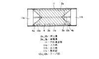
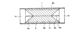
図13は例えば特開昭63−269601号公報に示された従来の円偏波発生器を示す正面図、図14は図13のXIV−XIV線に沿う断面図である。図において、円筒状の円形導波管1は、例えばアルミニウム等の金属により構成されている。また、円形導波管1は、送受信機(図示せず)に接続される入力端1a、アンテナ(図示せず)に接続される出力端1b、及び入力端1aと出力端1bとの間に設けられている厚肉部1cを有している。
【0003】
厚肉部1cは、入出力端1a,1bよりも内径を小さくすることにより肉厚が厚くされている。厚肉部1cの内周面には、それぞれ円形導波管1の軸方向(図14の左右方向)に沿って延びる一対の挿入溝2a,2b及び一対の補償溝3a,3bが設けられている。
【0004】
一対の挿入溝2a,2bは、互いに対向するように円形導波管1の周方向に180度の間隔をおいて配置されている。また、一対の補償溝3a,3bも、互いに対向するように円形導波管1の周方向に180度の間隔をおいて配置されている。さらに、挿入溝2a,2bと補償溝3a,3bとは、円形導波管1の周方向に90度の間隔をおいて配置されている。
【0005】
一対の挿入溝2a,2bには、誘電体板4の端部が挿入され固定されている。誘電体板4は、例えばポリテトラフルオロエチレン系樹脂により構成されている。円形導波管1の軸方向における誘電体板4の両端部には、テーパ状(三角形)の切欠部4a,4bが設けられている。
【0006】
次に、動作について説明する。まず、円形導波管1の基本モードであるTE11モードの電界方向が誘電体板4と45度の角度をなすように、入射波が入力端1aから入射するものとする。このとき、入射波の電界は、誘電体板4に平行な成分と垂直な成分とにほぼ等しい振幅で分解することができる。
【0007】
これらの成分うち、誘電体板4に平行な電界成分は、円形導波管1を通過する途中で誘電体板4の誘電率の効果により、誘電体板4に垂直な電界成分に比べて通過位相が遅れる。従って、誘電体板4の設置区間の長さを所定の値に設定すれば、誘電体板4に平行な電界成分の通過位相を誘電体板4に垂直な電界成分のそれに比べて90度遅らせることが可能となり、出力端1bから円偏波が取り出される。
【0008】
ところで、完全な円偏波を得るためには、誘電体板4に平行な電界成分に対する垂直電界成分の位相差を、使用する全周波数に渡って90度に設定する必要がある。また、例えば20GHz帯で受信、30GHz帯で送信を行う送受共用アンテナを構成する場合などには、離れた2つの周波数帯で上記位相差を90度にする必要が生じる。
【0009】
このような要求に対して、一般に誘電体板4により直交する2つの偏波間に位相差をつける構成では、誘電体板4の誘電率による波長短縮効果と円形導波管1の管内波長の周波数分散性との相互作用により、図15に示すような良好な周波数−位相差特性を得易いことが知られている。
【0010】
一方、実際の構成においては、誘電体板4の取付及び固定のために、円形導波管1の内壁に挿入溝2a,2bが必要となる。これら挿入溝2a,2bは、使用周波数が高くなるにつれてその存在が無視できなくなり、上記の周波数−位相差特性への影響が大きくなる。
【0011】
図13及び図14に示した構成では、挿入溝2a,2bによる特性劣化を補償する目的で、補償溝3a,3bが設けられている。補償溝3a,3bは、誘電体板4の面と垂直な面内の円形導波管1内壁に設けられている。これら4つの溝2a,2b,3a,3bは、円形導波管1の内壁に90度ずつの間隔で対称的に配置され、直交する2つの電界成分に同等の影響を与える。
【0012】
このため、溝2a,2b,3a,3bの大きさを最適に設定すれば、溝2a,2b,3a,3bを設けることによる直交電界成分間の位相差の相対変化を相殺することができる。このとき、図13及び図14の円偏波発生器では、内部の直交電界成分の位相関係が誘電体板4のみを設けた場合と等価となり、図15に示すような優れた位相差特性が得られる。
【0013】
【発明が解決しようとする課題】
上記のように構成された従来の円偏波発生器においては、誘電体板4の端部形状がテーパ状に徐々に変化しているの対して、溝2a,2b,3a,3bを設けるための厚肉部1cの両端部には、段差が生じている。円形導波管1の断面径は、使用周波数が高くなるほど小さくなるが、挿入溝2a,2bの深さは、誘電体板4をしっかりと固定する必要があるため、使用周波数によらず殆ど変わらない。従って、厚肉部1cの両端部に生じる段差は、使用周波数が高くなり、円形導波管1の断面径が小さくなるほど無視できなくなり、反射特性に影響を及ぼす。
【0014】
この発明は、上記のような問題点を解決することを課題としてなされたものであり、使用周波数が高くても反射特性を向上させることができる円偏波発生器を得ることを目的とする。
【0015】
【課題を解決するための手段】
この発明に係る円偏波発生器は、入力端と、出力端と、これら入力端と出力端との間に配置され、入力端及び出力端よりも内径を小さくすることにより肉厚が厚くされている厚肉部と、この厚肉部の内周面に設けられ、軸方向に延び互いに対向する一対の挿入溝と、これら挿入溝に対して周方向に90度の間隔をおいて厚肉部の内周面に設けられ、軸方向に延び互いに対向する一対の補償溝とを有する筒状の導波管、及びこの導波管内に配置され、両端部が挿入溝に挿入され固定されている誘電体板を備え、導波管の軸方向における厚肉部の少なくとも一端部では、端部へ向けて内径が徐々に広がり、挿入溝及び補償溝の深さが徐々に浅くなっているものである。
【0016】
また、導波管の軸方向における厚肉部の少なくとも一端部には、端部へ向けて内径が連続的に徐々に広がり、挿入溝及び補償溝の深さが連続的に徐々に浅くなるようにテーパ部が設けられている。
【0017】
さらに、導波管の軸方向における厚肉部の少なくとも一端部には、端部へ向けて内径が段階的に徐々に広がり、挿入溝及び補償溝の深さが段階的に徐々に浅くなるようにステップ部が設けられている。
さらにまた、ステップ部では、内径を変える管軸方向の間隔が、導波管の管内波長の1/4に設定されている。
【0018】
また、補償溝の深さは、挿入溝の深さよりも深く設定されている。
さらに、厚肉部の少なくとも一端部では、補償溝の深さが0となるまで内径が広げられている。
さらにまた、厚肉部の少なくとも一端部では、挿入溝の深さが0となるまで内径が広げられており、補償溝は、その底部が入力端及び出力端の内周面よりも径方向外側に位置するように設けられており、補償溝の端部には、深さが連続的に徐々に浅くなるように傾斜部が設けられている。
また、補償溝の幅は、挿入溝の幅よりも大きく設定されている。
さらに、補償溝には、誘電体が充填されている。
【0019】
【発明の実施の形態】
以下、この発明の実施の形態を図について説明する。
実施の形態1.
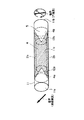
図1はこの発明の実施の形態1による円偏波発生器を示す正面図、図2は図1のII−II線に沿う断面図、図3は図1の円偏波発生器を示す概略の斜視図である。
【0020】
図において、円筒状の円形導波管11は、例えばアルミニウム等の金属により構成されている。また、円形導波管11は、送受信機(図示せず)に接続される入力端11a、アンテナ(図示せず)に接続される出力端11b、及び入力端11aと出力端11bとの間に設けられている厚肉部11cを有している。
【0021】
厚肉部11cは、入出力端11a,11bよりも内径を小さくすることにより肉厚が厚くされている。厚肉部11cの内周面には、それぞれ円形導波管11の軸方向(図2の左右方向)に沿って延びる一対の挿入溝2a,2b及び一対の補償溝3a,3bが設けられている。
【0022】
一対の挿入溝2a,2bは、互いに対向するように円形導波管1の周方向に180度の間隔をおいて配置されている。また、一対の補償溝3a,3bも、互いに対向するように円形導波管1の周方向に180度の間隔をおいて配置されている。さらに、挿入溝2a,2bと補償溝3a,3bとは、円形導波管1の周方向に90度の間隔をおいて配置されている。
【0023】
一対の挿入溝2a,2bには、誘電体板4の端部が挿入され固定されている。誘電体板4は、例えばポリテトラフルオロエチレン系樹脂により構成されている。円形導波管1の軸方向における誘電体板4の両端部には、テーパ状(三角形)の切欠部4a,4bが設けられている。
【0024】
円形導波管11の軸方向における厚肉部11cの両端部には、端部へ向けて内径が連続的に徐々に広がるようなテーパ部12a,12bが設けられている。厚肉部11cの内径は、厚肉部11cの両端部では入力端11a及び出力端11bの内径と等しくなっている。このように、テーパ部12a,12bを設けたことにより、溝2a,2b,3a,3bの深さは、長さ方向の両端部で連続的に徐々に浅くなり、最終的には0となっている。
【0025】
次に、動作について説明する。まず、円形導波管11の基本モードであるTE11モードの電界方向が誘電体板4と45度の角度をなすように、入射波が入力端1aから入射するものとする。このとき、入射波の電界は、誘電体板4に平行な成分と垂直な成分とにほぼ等しい振幅で分解することができる。
【0026】
これらの成分うち、誘電体板4に平行な電界成分は、円形導波管11を通過する途中で誘電体板4の誘電率の効果により、誘電体板4に垂直な電界成分に比べて通過位相が遅れる。従って、誘電体板4の設置区間の長さを所定の値に設定すれば、誘電体板4に平行な電界成分の通過位相を誘電体板4に垂直な電界成分のそれに比べて90度遅らせることが可能となり、出力端11bから円偏波が取り出される。
【0027】
ところで、完全な円偏波を得るためには、誘電体板4に平行な電界成分に対する垂直電界成分の位相差を、使用する全周波数に渡って90度に設定する必要がある。また、例えば20GHz帯で受信、30GHz帯で送信を行う送受共用アンテナを構成する場合などには、離れた2つの周波数帯で上記位相差を90度にする必要が生じる。
【0028】
このような要求に対して、一般に誘電体板4により直交する2つの偏波間に位相差をつける構成では、誘電体板4の誘電率による波長短縮効果と円形導波管1の管内波長の周波数分散性との相互作用により、図15に示すような良好な周波数−位相差特性を得易いことが知られている。
【0029】
一方、実際の構成においては、誘電体板4の取付及び固定のために、円形導波管11の内壁に挿入溝2a,2bが必要となる。これら挿入溝2a,2bは、使用周波数が高くなるにつれてその存在が無視できなくなり、上記の周波数−位相差特性への影響が大きくなる。
【0030】
図1ないし図3に示した構成では、挿入溝2a,2bによる特性劣化を補償する目的で、補償溝3a,3bが設けられている。補償溝3a,3bは、誘電体板4の面と垂直な面内の円形導波管1内壁に設けられている。これら4つの溝2a,2b,3a,3bは、円形導波管1の内壁に90度ずつの間隔で対称的に配置され、直交する2つの電界成分に同等の影響を与える。
【0031】
このため、溝2a,2b,3a,3bの大きさを最適に設定すれば、溝2a,2b,3a,3bを設けることによる直交電界成分間の位相差の相対変化を相殺することができる。このとき、図1ないし図3の円偏波発生器では、内部の直交電界成分の位相関係が誘電体板4のみを設けた場合と等価となり、図15に示すような優れた位相差特性が得られる。
【0032】
また、実施の形態1では、溝2a,2b,3a,3bを設けるための厚肉部11cの両端部にテーパ部12a,12bが設けられており、厚肉部11cの内周面と入力端11a及び出力端の内周面との間に段差が生じるのが防止されている。このため、使用周波数が高い場合でも、反射を生じず、反射特性を向上させることができる。
【0033】
さらに、テーパ部12a,12bは、円形導波管11の長手方向における厚肉部11cの両端部に設けられているため、送受信の両方向において反射特性を向上させることができる。
【0034】
なお、テーパ部は、厚肉部の一端部のみに設けてもよく、テーパ部を設けない場合に比べれば、反射特性をある程度向上させることができる。
【0035】
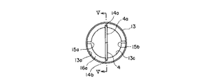
実施の形態2.
次に、図4はこの発明の実施の形態2による円偏波発生器を示す正面図、図5は図4のV−V線に沿う断面図である。図において、円形導波管13は、入力端13a、出力端13b、及び厚肉部13cを有している。厚肉部13cには、それぞれ円形導波管12の軸方向(図5の左右方向)に沿って延びる一対の挿入溝14a,14b及び一対の補償溝15a,15bが設けられている。
【0036】
一対の挿入溝14a,14bは、互いに対向するように円形導波管1の周方向に180度の間隔をおいて配置されている。また、一対の補償溝15a,15bも、互いに対向するように円形導波管1の周方向に180度の間隔をおいて配置されている。さらに、挿入溝14a,14bと補償溝15a,15bとは、円形導波管1の周方向に90度の間隔をおいて配置されている。一対の挿入溝14a,14bには、誘電体板4の端部が挿入され固定されている。
【0037】
円形導波管13の軸方向における厚肉部13cの両端部には、端部へ向けて内径が連続的に徐々に広がるようなテーパ部16a,16bが設けられている。厚肉部13cの内径は、厚肉部13cの両端部では入力端13a及び出力端13bの内径と等しくなっている。また、挿入溝14a,14bの深さは、誘電体板4を保持し固定するために必要最小限の深さになっており、補償溝15a,15bの深さは、挿入溝14a,14bよりも深く設定されている。
【0038】
このような円偏波発生器では、誘電体板4が挿入されている挿入溝14a,14bの深さは、誘電率の効果により、実際の深さよりも等価的に深く見える。これに対し、補償溝15a,15bの深さを挿入溝14a,14bよりも深くすることで、円形導波管13内を伝搬する電波に対して与える影響を同等にすることができる。なお、テーパ部16a,16bの内径は、深い方の溝、即ち補償溝15a,15bの両端部の深さが最終的に0となるまで広げられている。
【0039】
このように、補償溝15a,15bの深さを挿入溝14a,14bよりも深くすることにより、4つの溝14a,14b,15a,15bの電気的な関係がより正確に対称となるため、位相差特性をさらに向上させることができる。
【0040】
なお、実施の形態2では、補償溝15a,15bの深さを挿入溝14a,14bと異なるものとしたが、深さ及び幅を異なるものとしたり、幅のみを異なるものとすることにより、電波に対して与える影響を同等にすることもできる。即ち、補償溝15a,15bの幅を挿入溝14a,14bの幅よりも大きくしてもよい。
【0041】
実施の形態3.
次に、図6はこの発明の実施の形態3による円偏波発生器を示す正面図、図7は図6のVII−VII線に沿う断面図、図8は図6のVIII−VIII線に沿う断面図である。図において、円形導波管17は、入力端17a、出力端17b、及び厚肉部17cを有している。厚肉部17cには、それぞれ円形導波管12の軸方向(図5の左右方向)に沿って延びる一対の挿入溝18a,18b及び一対の補償溝19a,19bが設けられている。
【0042】
一対の挿入溝18a,18bは、互いに対向するように円形導波管1の周方向に180度の間隔をおいて配置されている。また、一対の補償溝19a,19bも、互いに対向するように円形導波管1の周方向に180度の間隔をおいて配置されている。さらに、挿入溝18a,18bと補償溝19a,19bとは、円形導波管1の周方向に90度の間隔をおいて配置されている。一対の挿入溝18a,18bには、誘電体板4の端部が挿入され固定されている。
【0043】
円形導波管17の軸方向における厚肉部17cの両端部には、端部へ向けて内径が連続的に徐々に広がるようなテーパ部20a,20bが設けられている。厚肉部17cの内径は、厚肉部17cの両端部では入力端17a及び出力端17bの内径と等しくなっている。また、挿入溝18a,18bの深さは、誘電体板4を保持し固定するために必要最小限の深さになっており、補償溝19a,19bの深さは、挿入溝18a,18bよりも深く設定されている。
【0044】
さらに、補償溝19a,19bの両端部には、端部へ向けて深さが連続的に徐々に浅くなるような傾斜部21がそれぞれ設けられている。実施の形態2では、厚肉部13cの内径と入出力端13a,13bの内径との差を大きくすることにより、深さの異なる溝14a,14b,15a,15bを厚肉部13cに設けた。これに対して、実施の形態3では、円形導波管17全体の肉厚を厚くし、深い方の補償溝19a,19bを挿入溝18a,18bよりも掘り下げる構造としている。
【0045】
従って、補償溝19a,19bの底面は、入出力端17a,17bの内周面よりも径方向外側に位置している。そして、補償溝19a,19bの両端部と入出力端17a,17bの内周面との間に段部が生じないように、補償溝19a,19bの両端部に傾斜部21が設けられている。
【0046】
このような円偏波発生器では、補償溝19a,19bの深さを挿入溝18a,18bよりも深くすることにより、4つの溝18a,18b,19a,19bの電気的な関係がより正確に対称となるため、位相差特性をさらに向上させることができる。
【0047】
また、円形導波管17全体の肉厚を厚くし、補償溝19a,19bの底面が入出力端17a,17bの内周面よりも径方向外側に位置するように補償溝19a,19bが掘り下げられているため、厚肉部17cと入出力端17a,17bとの内径の差を小さく抑えることができ、反射特性を向上させることができる。さらに、補償溝19a,19bの両端部に傾斜部21を設けたので、反射特性をさらに向上させることができる。
【0048】
なお、実施の形態3では、補償溝19a,19bの深さを挿入溝18a,18bと異なるものとしたが、深さ及び幅を異なるものとしたり、幅のみを異なるものとすることにより、電波に対して与える影響を同等にすることもできる。
【0049】
実施の形態4.
次に、図9はこの発明の実施の形態4による円偏波発生器を示す正面図、図10は図9のX−X線に沿う断面図である。図において、円形導波管22は、入力端22a、出力端22b、及び厚肉部22cを有している。厚肉部22cには、それぞれ円形導波管12の軸方向(図5の左右方向)に沿って延びる一対の挿入溝23a,23b及び一対の補償溝24a,24bが設けられている。
【0050】
一対の挿入溝23a,23bは、互いに対向するように円形導波管1の周方向に180度の間隔をおいて配置されている。また、一対の補償溝24a,24bも、互いに対向するように円形導波管1の周方向に180度の間隔をおいて配置されている。さらに、挿入溝23a,23bと補償溝24a,24bとは、円形導波管1の周方向に90度の間隔をおいて配置されている。一対の挿入溝23a,23bには、誘電体板4の端部が挿入され固定されている。
【0051】
円形導波管22の軸方向における厚肉部22cの両端部には、端部へ向けて内径が段階的に徐々に広がるようなステップ部25a,25bが設けられている。このように、ステップ部25a,25bを設けたことにより、溝23a,23b,24a,24bの深さは、長さ方向の両端部で段階的に徐々に浅くなる。
【0052】
また、ステップ部25a,25bにおいて内径を変える管軸方向の間隔は、円形導波管22の管内波長の1/4に設定されている。これにより、1/4インピーダンス変成器が構成される。
【0053】
このような円偏波発生器では、ステップ部25a,25bにより1/4インピーダンス変成器が構成されるため、実施の形態1のようなテーパ部4a,4bを設けた場合に比べて、全長を短くすることができるとともに、広帯域に渡って反射を小さく抑え、反射特性を向上させることができる。
【0054】
なお、ステップ部25a,25bは、厚肉部22cの両端部に設けるのが好適であるが、場合によっては一端部のみに設けてもよく、反射特性をある程度向上させることができる。
【0055】
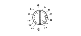
実施の形態5.
次に、図11はこの発明の実施の形態5による円偏波発生器を示す正面図、図12は図11のXII−XII線に沿う断面図である。図において、補償溝3a,3bには、誘電体26がそれぞれ充填されている。誘電体26の誘電率は、誘電体板4の誘電率と等しく設定されている。補償溝3a,3bの端部において、誘電体26には、テーパ部12a,12bと面一となるように傾斜が設けられている。他の構成は、実施の形態1と同様である。
【0056】
このような円偏波発生器では、補償溝3a,3bに誘電体26が充填されているため、補償溝3a,3bの深さが挿入溝2a,2bの深さと同程度であっても、円形導波管11内を伝搬する電波に対して与える影響を同等にすることができる。従って、位相差特性をさらに向上させることができる。
【0057】
なお、実施の形態5では、挿入溝2a,2bと補償溝3a,3bとの深さ及び幅が等しく、かつ誘電体板4と誘電体26との誘電率が等しい場合を示したが、挿入溝2a,2bと補償溝3a,3bの深さや幅が異なる場合でも、誘電体板4と誘電体26との誘電率を最適に設定することにより、同様の効果を得ることができる。
【0058】
また、実施の形態5では、誘電体26の端部をテーパ部12a,12bに揃えたが、必ずしも揃えなくてもよい。
【0059】
【発明の効果】
以上説明したように、この発明の円偏波発生器は、導波管の軸方向における厚肉部の少なくとも一端部で、端部へ向けて内径が徐々に広げられ、挿入溝及び補償溝の深さが徐々に浅くされているため、厚肉部の端部に段部が生じず、使用周波数が高くても反射特性を向上させることができる。
【0060】
また、導波管の軸方向における厚肉部の少なくとも一端部には、端部へ向けて内径が連続的に徐々に広がり、挿入溝及び補償溝の深さが連続的に徐々に浅くなるようにテーパ部が設けられているので、簡単な構造により、反射特性を向上させることができる。
【0061】
さらに、導波管の軸方向における厚肉部の少なくとも一端部には、端部へ向けて内径が段階的に徐々に広がり、挿入溝及び補償溝の深さが段階的に徐々に浅くなるようにステップ部が設けられているので、簡単な構造により、反射特性を向上させることができる。
【0062】
さらにまた、ステップ部では、内径を変える管軸方向の間隔が、導波管の管内波長の1/4に設定されているので、簡単な構造により、反射特性を向上させることができる。
【0063】
また、補償溝の深さは、挿入溝の深さよりも深く設定されているので、挿入溝及び補償溝の電気的な関係がより正確に対称となり、位相差特性をさらに向上させることができる。
【0064】
さらに、厚肉部の少なくとも一端部では、補償溝の深さが0となるまで内径が広げられているので、挿入溝及び補償溝の電気的な関係がより正確に対称となり、位相差特性をさらに向上させることができる。
【0065】
さらにまた、厚肉部の少なくとも一端部では、挿入溝の深さが0となるまで内径が広げられており、補償溝は、その底部が入力端及び出力端の内周面よりも径方向外側に位置するように設けられいるので、厚肉部と入出力端との内径の差を小さく抑えることができ、反射特性を向上させることができる。また、補償溝の両端部に傾斜部を設けたので、反射特性をさらに向上させることができる。
【0066】
また、補償溝の幅は、挿入溝の幅よりも大きく設定されているので、挿入溝及び補償溝の電気的な関係がより正確に対称となり、位相差特性をさらに向上させることができる。
【0067】
さらに、補償溝には誘電体が充填されているので、補償溝の深さが挿入溝の深さと同程度であっても、導波管内を伝搬する電波に対して与える影響を同等にすることができ、位相差特性をさらに向上させることができる。
【図面の簡単な説明】
【図1】 この発明の実施の形態1による円偏波発生器を示す正面図である。
【図2】 図1のII−II線に沿う断面図である。
【図3】 図1の円偏波発生器を示す概略の斜視図である。
【図4】 この発明の実施の形態2による円偏波発生器を示す正面図である。
【図5】 図4のV−V線に沿う断面図である。
【図6】 この発明の実施の形態3による円偏波発生器を示す正面図である。
【図7】 図6のVII−VII線に沿う断面図である。
【図8】 図6のVIII−VIII線に沿う断面図である。
【図9】 この発明の実施の形態4による円偏波発生器を示す正面図である。
【図10】 図9のX−X線に沿う断面図である。
【図11】 この発明の実施の形態5による円偏波発生器を示す正面図である。
【図12】 図11のXII−XII線に沿う断面図である。
【図13】 従来の円偏波発生器の一例を示す正面図である。
【図14】 図13のXIV−XIV線に沿う断面図である。
【図15】 円形導波管における周波数−位相差特性の一例を示すグラフである。
【符号の説明】
11,13,17,22 円形導波管、11a,13a,17a,22a 入力端、11b,13b,17b,22b 出力端、11c,13c,17c,22c 厚肉部、2a,2b,14a,14b,18a,18b,23a,23b挿入溝、3a,3b,15a,15b,19a,19b,24a,24b 補償溝、12a,12b,16a,16b,20a,20b テーパ部、21 傾斜部、25a,25b ステップ部、26 誘電体。[0001]
BACKGROUND OF THE INVENTION
The present invention relates to a waveguide-type circularly polarized wave generator used mainly in the microwave band and other frequency bands in the VHF band, the UHF band, and the millimeter wave band.
[0002]
[Prior art]
FIG. 13 is a front view showing a conventional circularly polarized wave generator disclosed in, for example, Japanese Patent Laid-Open No. 63-269601, and FIG. 14 is a sectional view taken along line XIV-XIV in FIG. In the figure, a cylindrical
[0003]
The thick portion 1c is thickened by making the inner diameter smaller than the input / output ends 1a and 1b. A pair of
[0004]
The pair of
[0005]
The ends of the
[0006]
Next, the operation will be described. First, it is assumed that an incident wave is incident from the input end 1a so that the electric field direction of the TE11 mode, which is the fundamental mode of the
[0007]
Among these components, the electric field component parallel to the
[0008]
By the way, in order to obtain complete circular polarization, it is necessary to set the phase difference of the vertical electric field component with respect to the electric field component parallel to the
[0009]
In response to such a requirement, in general, in a configuration in which a phase difference is provided between two polarized waves orthogonal to each other by the
[0010]
On the other hand, in the actual configuration, the insertion grooves 2 a and 2 b are required on the inner wall of the
[0011]
In the configuration shown in FIGS. 13 and 14,
[0012]
For this reason, if the size of the
[0013]
[Problems to be solved by the invention]
In the conventional circularly polarized wave generator configured as described above, the
[0014]
An object of the present invention is to provide a circularly polarized wave generator capable of improving the reflection characteristics even when the operating frequency is high.
[0015]
[Means for Solving the Problems]
The circularly polarized wave generator according to the present invention is disposed between the input end, the output end, and the input end and the output end, and is made thicker by making the inner diameter smaller than the input end and the output end. A thick wall portion, a pair of insertion grooves provided on the inner peripheral surface of the thick wall portion, extending in the axial direction and facing each other, and with a thickness of 90 degrees in the circumferential direction with respect to the insertion grooves. A cylindrical waveguide having a pair of compensation grooves extending in the axial direction and facing each other, and both ends are inserted and fixed in the insertion groove. In at least one end of the thick-walled portion in the axial direction of the waveguide, the inner diameter gradually increases toward the end, and the depth of the insertion groove and the compensation groove gradually decreases. It is.
[0016]
Further, at least one end of the thick wall portion in the axial direction of the waveguide is such that the inner diameter continuously and gradually expands toward the end portion, and the depth of the insertion groove and the compensation groove gradually decreases gradually. Is provided with a taper portion.
[0017]
Further, at least one end portion of the thick-walled portion in the axial direction of the waveguide is such that the inner diameter gradually increases toward the end portion, and the depth of the insertion groove and the compensation groove gradually decreases. Is provided with a step portion.
Furthermore, in the step portion, the interval in the tube axis direction for changing the inner diameter is set to ¼ of the in-tube wavelength of the waveguide.
[0018]
The depth of the compensation groove is set deeper than the depth of the insertion groove.
Further, at least one end of the thick portion has an inner diameter that is expanded until the depth of the compensation groove becomes zero.
Furthermore, at least one end of the thick wall portion has an inner diameter that is expanded until the depth of the insertion groove becomes zero, and the compensation groove has a bottom portion radially outside the inner peripheral surfaces of the input end and the output end. In the end portion of the compensation groove, an inclined portion is provided so that the depth gradually decreases gradually.
The width of the compensation groove is set larger than the width of the insertion groove.
Further, the compensation groove is filled with a dielectric.
[0019]
DETAILED DESCRIPTION OF THE INVENTION
Embodiments of the present invention will be described below with reference to the drawings.
1 is a front view showing a circularly polarized wave generator according to
[0020]
In the figure, a cylindrical circular waveguide 11 is made of a metal such as aluminum. The circular waveguide 11 includes an input end 11a connected to a transceiver (not shown), an output end 11b connected to an antenna (not shown), and between the input end 11a and the output end 11b. It has the thick part 11c provided.
[0021]
The thick portion 11c is thickened by making the inner diameter smaller than the input / output ends 11a and 11b. A pair of
[0022]
The pair of
[0023]
The ends of the
[0024]
At both ends of the thick portion 11c in the axial direction of the circular waveguide 11,
[0025]
Next, the operation will be described. First, it is assumed that an incident wave is incident from the input end 1a so that the electric field direction of the TE11 mode, which is the fundamental mode of the circular waveguide 11, forms an angle of 45 degrees with the
[0026]
Among these components, the electric field component parallel to the
[0027]
By the way, in order to obtain complete circular polarization, it is necessary to set the phase difference of the vertical electric field component with respect to the electric field component parallel to the
[0028]
In response to such a requirement, in general, in a configuration in which a phase difference is provided between two polarized waves orthogonal to each other by the
[0029]
On the other hand, in the actual configuration, the
[0030]
In the configuration shown in FIGS. 1 to 3, the
[0031]
For this reason, if the size of the
[0032]
In the first embodiment, the
[0033]
Furthermore, since the
[0034]
The tapered portion may be provided only at one end of the thick portion, and the reflection characteristics can be improved to some extent as compared with the case where the tapered portion is not provided.
[0035]
Embodiment 2. FIG.
4 is a front view showing a circularly polarized wave generator according to Embodiment 2 of the present invention, and FIG. 5 is a cross-sectional view taken along the line V-V in FIG. In the figure, the
[0036]
The pair of
[0037]
Tapered portions 16a and 16b are provided at both ends of the
[0038]
In such a circularly polarized wave generator, the depths of the
[0039]
Thus, by making the depth of the
[0040]
In the second embodiment, the depth of the
[0041]
6 is a front view showing a circularly polarized wave generator according to
[0042]
The pair of
[0043]
[0044]
Furthermore, inclined
[0045]
Accordingly, the bottom surfaces of the
[0046]
In such a circularly polarized wave generator, the electrical relationship between the four
[0047]
Further, the thickness of the entire
[0048]
In the third embodiment, the depth of the
[0049]
9 is a front view showing a circularly polarized wave generator according to
[0050]
The pair of
[0051]
[0052]
Further, the interval in the tube axis direction for changing the inner diameter in the
[0053]
In such a circularly polarized wave generator, since the quarter impedance transformer is configured by the
[0054]
The
[0055]
11 is a front view showing a circularly polarized wave generator according to
[0056]
In such a circularly polarized wave generator, since the
[0057]
In the fifth embodiment, the
[0058]
In the fifth embodiment, the end portions of the dielectric 26 are aligned with the
[0059]
【The invention's effect】
As described above, the circularly polarized wave generator according to the present invention has an inner diameter gradually widened toward the end portion at least at one end portion of the thick portion in the axial direction of the waveguide. Since the depth is gradually reduced, no step portion is formed at the end of the thick portion, and the reflection characteristics can be improved even when the operating frequency is high.
[0060]
Further, at least one end of the thick wall portion in the axial direction of the waveguide is such that the inner diameter continuously and gradually expands toward the end portion, and the depth of the insertion groove and the compensation groove gradually decreases gradually. Since the taper portion is provided, the reflection characteristics can be improved with a simple structure.
[0061]
Further, at least one end portion of the thick-walled portion in the axial direction of the waveguide is such that the inner diameter gradually increases toward the end portion, and the depth of the insertion groove and the compensation groove gradually decreases. Since the step portion is provided, the reflection characteristics can be improved with a simple structure.
[0062]
Furthermore, in the step portion, the interval in the tube axis direction for changing the inner diameter is set to ¼ of the in-tube wavelength of the waveguide, so that the reflection characteristics can be improved with a simple structure.
[0063]
Further, since the depth of the compensation groove is set deeper than the depth of the insertion groove, the electrical relationship between the insertion groove and the compensation groove is more accurately symmetric, and the phase difference characteristics can be further improved.
[0064]
Furthermore, since the inner diameter is expanded until the depth of the compensation groove becomes zero at least at one end of the thick part, the electrical relationship between the insertion groove and the compensation groove becomes more accurate and the phase difference characteristic is improved. Further improvement can be achieved.
[0065]
Furthermore, at least one end of the thick wall portion has an inner diameter that is expanded until the depth of the insertion groove becomes zero, and the compensation groove has a bottom portion radially outside the inner peripheral surfaces of the input end and the output end. Therefore, the difference in inner diameter between the thick wall portion and the input / output end can be kept small, and the reflection characteristics can be improved. In addition, since the inclined portions are provided at both ends of the compensation groove, the reflection characteristics can be further improved.
[0066]
Further, since the width of the compensation groove is set larger than the width of the insertion groove, the electrical relationship between the insertion groove and the compensation groove becomes more accurate and the phase difference characteristic can be further improved.
[0067]
In addition, since the compensation groove is filled with a dielectric, even if the depth of the compensation groove is about the same as the depth of the insertion groove, the effect on the radio wave propagating in the waveguide should be made equal. And the phase difference characteristics can be further improved.
[Brief description of the drawings]
FIG. 1 is a front view showing a circularly polarized wave generator according to
2 is a cross-sectional view taken along the line II-II in FIG.
FIG. 3 is a schematic perspective view showing the circularly polarized wave generator of FIG. 1;
FIG. 4 is a front view showing a circularly polarized wave generator according to Embodiment 2 of the present invention.
5 is a cross-sectional view taken along line VV in FIG.
FIG. 6 is a front view showing a circularly polarized wave generator according to
7 is a cross-sectional view taken along line VII-VII in FIG.
8 is a cross-sectional view taken along line VIII-VIII in FIG.
FIG. 9 is a front view showing a circularly polarized wave generator according to
10 is a cross-sectional view taken along line XX of FIG.
FIG. 11 is a front view showing a circularly polarized wave generator according to
12 is a cross-sectional view taken along line XII-XII in FIG.
FIG. 13 is a front view showing an example of a conventional circularly polarized wave generator.
14 is a cross-sectional view taken along line XIV-XIV in FIG.
FIG. 15 is a graph showing an example of frequency-phase difference characteristics in a circular waveguide.
[Explanation of symbols]
11, 13, 17, 22 Circular waveguide, 11a, 13a, 17a, 22a Input end, 11b, 13b, 17b, 22b Output end, 11c, 13c, 17c, 22c Thick part, 2a, 2b, 14a,
Claims (9)
この導波管内に配置され、両端部が上記挿入溝に挿入され固定されている誘電体板
を備え、上記導波管の軸方向における上記厚肉部の少なくとも一端部では、端部へ向けて内径が徐々に広がり、上記挿入溝及び上記補償溝の深さが徐々に浅くなっていることを特徴とする円偏波発生器。An input end, an output end, a thick portion disposed between the input end and the output end, and having a thickness increased by making the inner diameter smaller than the input end and the output end, and the thickness A pair of insertion grooves that extend in the axial direction and face each other, and are provided on the inner peripheral surface of the thick part at 90 ° intervals in the circumferential direction. A cylindrical waveguide having a pair of compensation grooves extending in the axial direction and facing each other, and a dielectric plate disposed in the waveguide and having both end portions inserted and fixed in the insertion groove, In at least one end portion of the thick portion in the axial direction of the waveguide, the inner diameter gradually increases toward the end portion, and the depth of the insertion groove and the compensation groove gradually decreases. Circular polarization generator.
Priority Applications (1)
| Application Number | Priority Date | Filing Date | Title |
|---|---|---|---|
| JP2001222710A JP3723751B2 (en) | 2001-07-24 | 2001-07-24 | Circular polarization generator |
Applications Claiming Priority (1)
| Application Number | Priority Date | Filing Date | Title |
|---|---|---|---|
| JP2001222710A JP3723751B2 (en) | 2001-07-24 | 2001-07-24 | Circular polarization generator |
Publications (2)
| Publication Number | Publication Date |
|---|---|
| JP2003037403A JP2003037403A (en) | 2003-02-07 |
| JP3723751B2 true JP3723751B2 (en) | 2005-12-07 |
Family
ID=19056148
Family Applications (1)
| Application Number | Title | Priority Date | Filing Date |
|---|---|---|---|
| JP2001222710A Expired - Fee Related JP3723751B2 (en) | 2001-07-24 | 2001-07-24 | Circular polarization generator |
Country Status (1)
| Country | Link |
|---|---|
| JP (1) | JP3723751B2 (en) |
Families Citing this family (1)
| Publication number | Priority date | Publication date | Assignee | Title |
|---|---|---|---|---|
| CN102629702B (en) * | 2012-04-12 | 2014-10-08 | 中国科学院光电技术研究所 | Artificial structure-based multi-frequency circular polarizer |
-
2001
- 2001-07-24 JP JP2001222710A patent/JP3723751B2/en not_active Expired - Fee Related
Also Published As
| Publication number | Publication date |
|---|---|
| JP2003037403A (en) | 2003-02-07 |
Similar Documents
| Publication | Publication Date | Title |
|---|---|---|
| US10218076B1 (en) | Hexagonal waveguide based circularly polarized horn antennas | |
| CA2292064C (en) | Line transition device between dielectric waveguide and waveguide, and oscillator and transmitter using the same | |
| JPWO2018029807A1 (en) | Array antenna device and manufacturing method of array antenna device | |
| US6507323B1 (en) | High-isolation polarization diverse circular waveguide orthomode feed | |
| US4356495A (en) | Corrugated antenna feedhorn with elliptical aperture | |
| US4442437A (en) | Small dual frequency band, dual-mode feedhorn | |
| US20050179593A1 (en) | Plane antenna and its designing method | |
| JP4753981B2 (en) | Waveguide / stripline converter | |
| JP3723751B2 (en) | Circular polarization generator | |
| EP1139489A1 (en) | Primary radiator having improved receiving efficiency by reducing side lobes | |
| WO2018115115A1 (en) | Millimeter wave antenna and connection arrangements | |
| EP0187671B1 (en) | Primary radiator for circularly polarized wave | |
| US5760658A (en) | Circular-linear polarizer including flat and curved portions | |
| RU2703605C1 (en) | Waveguide polarization selector with reduced longitudinal size | |
| EP2311133A1 (en) | Orthomode transducer for the reception of two orthogonally polarized waves | |
| JPH04134901A (en) | Input device for receiving both horizontally and vertically polarized waves | |
| JP3135049B2 (en) | Circularly polarized primary radiator | |
| JP7147536B2 (en) | radio wave transmission cable | |
| EP3340371A1 (en) | Connection arrangement | |
| KR100638738B1 (en) | Circularly polarized wave generator | |
| JP4053928B2 (en) | Circular-rectangular waveguide converter, demultiplexer for orthogonal polarization separation, primary radiator, feeder and antenna | |
| JP4103330B2 (en) | NRD guide L type antenna element | |
| JPH05299901A (en) | Circularly polarized wave device | |
| JPH0583029A (en) | Radial line slot antenna | |
| JP2001044713A (en) | Small-sized waveguide |
Legal Events
| Date | Code | Title | Description |
|---|---|---|---|
| A131 | Notification of reasons for refusal |
Free format text: JAPANESE INTERMEDIATE CODE: A131 Effective date: 20050118 |
|
| TRDD | Decision of grant or rejection written | ||
| A01 | Written decision to grant a patent or to grant a registration (utility model) |
Free format text: JAPANESE INTERMEDIATE CODE: A01 Effective date: 20050913 |
|
| A61 | First payment of annual fees (during grant procedure) |
Free format text: JAPANESE INTERMEDIATE CODE: A61 Effective date: 20050916 |
|
| R150 | Certificate of patent or registration of utility model |
Free format text: JAPANESE INTERMEDIATE CODE: R150 |
|
| FPAY | Renewal fee payment (event date is renewal date of database) |
Free format text: PAYMENT UNTIL: 20080922 Year of fee payment: 3 |
|
| FPAY | Renewal fee payment (event date is renewal date of database) |
Free format text: PAYMENT UNTIL: 20090922 Year of fee payment: 4 |
|
| FPAY | Renewal fee payment (event date is renewal date of database) |
Free format text: PAYMENT UNTIL: 20090922 Year of fee payment: 4 |
|
| FPAY | Renewal fee payment (event date is renewal date of database) |
Free format text: PAYMENT UNTIL: 20100922 Year of fee payment: 5 |
|
| FPAY | Renewal fee payment (event date is renewal date of database) |
Free format text: PAYMENT UNTIL: 20110922 Year of fee payment: 6 |
|
| FPAY | Renewal fee payment (event date is renewal date of database) |
Free format text: PAYMENT UNTIL: 20110922 Year of fee payment: 6 |
|
| FPAY | Renewal fee payment (event date is renewal date of database) |
Free format text: PAYMENT UNTIL: 20120922 Year of fee payment: 7 |
|
| FPAY | Renewal fee payment (event date is renewal date of database) |
Free format text: PAYMENT UNTIL: 20130922 Year of fee payment: 8 |
|
| LAPS | Cancellation because of no payment of annual fees |