JP3717536B2 - Signal amplifier and image display device - Google Patents
Signal amplifier and image display device Download PDFInfo
- Publication number
- JP3717536B2 JP3717536B2 JP11923894A JP11923894A JP3717536B2 JP 3717536 B2 JP3717536 B2 JP 3717536B2 JP 11923894 A JP11923894 A JP 11923894A JP 11923894 A JP11923894 A JP 11923894A JP 3717536 B2 JP3717536 B2 JP 3717536B2
- Authority
- JP
- Japan
- Prior art keywords
- circuit
- signal
- amplifier
- linear
- output
- Prior art date
- Legal status (The legal status is an assumption and is not a legal conclusion. Google has not performed a legal analysis and makes no representation as to the accuracy of the status listed.)
- Expired - Fee Related
Links
Images


Landscapes
- Amplifiers (AREA)
- Liquid Crystal Display Device Control (AREA)
Description
【0001】
【産業上の利用分野】
本発明は、入力に比例した出力が得られる信号増幅器および、この信号増幅器を使用した画像表示装置に関する。
【0002】
【従来の技術】
入力に比例した出力が得られるという線形特性を有する信号増幅器には、通常、オペレーショナル・アンプが使用されているが、素子数が少なくて済むカスコードアンプもしばしば使用されている。
【0003】
カスコードアンプは、例えば、マグロウヒル・ブック社が昭和57年7月10日に発行した「トランジスタとICのための電子回路(II)第2版」のp.324に記載されているように、2個の同種のバイポーラ・トランジスターを直列に接続した構成になっており、出力と入力とでは直流レベルが異なるが、交流成分は減衰しないという特徴を有している。
【0004】
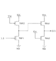
カスコードアンプを使用した信号増幅器の一例を図11に示す。
【0005】
この信号増幅器は、直列接続された2個のカスコードアンプを備えている。前段のカスコードアンプは、電源VCCとVSSとの間に直列に接続されたpチャンネル型トランジスターTRP1、TRP2からなっており、後段のカスコードアンプは、電源VCCとVSSとの間に直列に接続されたnチャンネル型トランジスターTRN1、TRN2からなっている。トランジスターTRP2、TRN2は、定電流源として働くように、それらのゲートには、それぞれ、所定の電圧Vbp、Vbnが印加されている。入力信号はトランジスターTRP1のゲート電極に印加され、出力信号はトランジスターTRN1、TRN2の接続点から取り出される。
【0006】
以上のように、2個のカスコードアンプを直列に設けることにより、出力レベルの変動が入力レベルに影響を与えないようなっている。
【0007】
上記の信号増幅器は、入力に比例した出力が得られるという特性を有しているため、様々な分野で利用されている。例えば、アクティブ・マトリクス型画像表示装置の分野では、映像信号をデータ信号線に書き込むデータ信号線駆動回路における、信号増幅器に使用されている。
【0008】
【発明が解決しようとする課題】
ところが、上記従来の信号増幅器では、入力信号のレベルが増大するレベル変化があったとき、そのレベル変化に高速応答した出力が得られるが、入力信号のレベルが減少するレベル変化があったとき、そのレベル変化に高速応答した出力が得られないという問題点を有している。
【0009】
このため、上記の信号増幅器をアクティブ・マトリクス型画像表示装置に利用した場合、所定の期間内に、映像信号をデータ信号線に書き込めなくなる恐れがある。特に、多階調表示を行う画像表示装置に利用した場合、表示品位の低下が起こりやすくなる。
【0010】
トランジスターTRN2の駆動能力を大きくすれば(つまり、トランジスターTRN2における定常電流を大きくすれば)、入力信号のレベルが減少するレベル変化があったときでも、そのレベル変化に高速応答した出力が得られる。しかしながら、トランジスターTRN2の駆動能力を大きくすれば、消費電力が増大するという新たな問題を招来する。
【0011】
特に、絶縁基板上の多結晶シリコン薄膜に形成されたトランジスターでは、単結晶シリコン基板上に形成されたトランジスターに比べて、キャリア移動度が低く、閾値電圧が高く、耐圧が低いため、トランジスターTRN2の駆動能力をある程度以上に大きくすることは困難である。
【0012】
したがって、大画面化およびコストダウンのため、絶縁基板上の多結晶シリコン薄膜に画素アレイや駆動回路をモノリシックに形成したアクティブ・マトリクス型画像表示装置を実現しようとしても、従来の信号増幅器ではそれを実現することは困難であるという問題点を有している。
【0013】
【課題を解決するための手段】
請求項1の発明に係る信号増幅器は、上記の課題を解決するために、互いに並列接続され、それぞれ入力信号を線形増幅する第1、第2の増幅回路が設けられており、入力信号のレベルが増大するレベル変化に対する応答速度は、第1の増幅回路の方が第2の増幅回路よりも大きくなるように設定されており、入力信号のレベルが減少するレベル変化に対する応答速度は、第2の増幅回路の方が第1の増幅回路よりも大きくなるように設定されており、前記の第1の増幅回路は、入力信号を線形増幅するpチャンネル型トランジスターからなる第1の線形回路と、第1の線形回路の出力信号を線形増幅するnチャンネル型トランジスターからなる第2の線形回路とを含んでおり、前記の第2の増幅回路は、入力信号を線形増幅するnチャンネル型トランジスターからなる第3の線形回路と、第3の線形回路の出力信号を線形増幅するpチャンネル型トランジスターからなる第4の線形回路とを含んでいることを特徴としている。
【0014】
請求項2の発明に係る信号増幅器は、上記の課題を解決するために、請求項1の信号増幅器であって、前記の第1、第2の増幅回路が、シリコン薄膜に形成されていることを特徴としている。
【0015】
請求項3の発明に係る画像表示装置は、上記の課題を解決するために、マトリクス状に配置された複数の表示素子と、映像信号をデータ信号線に出力するデータ信号線駆動回路と、走査信号を走査信号線に出力する走査信号線駆動回路と、表示素子毎に設けられ、データ信号線上の映像信号を走査信号線上の走査信号に応じて表示素子に出力するスイッチング素子とが備えられており、上記のデータ信号線駆動回路は、映像信号を線形増幅しデータ信号線に出力する信号増幅器として、請求項1または2に記載の信号増幅器を含んでいることを特徴としている。
【0016】
【作用】
請求項1の構成によれば、入力信号を線形増幅できる。しかも、入力信号のレベルが増大するレベル変化があったとき、そのレベル変化に高速応答した出力が第1の増幅回路から得られ、入力信号のレベルが減少するレベル変化があったとき、そのレベル変化に高速応答した出力が第2の増幅回路から得られる。つまり、入力信号のレベル変化に関わらず、入力信号に高速応答した出力を得ることができる。
【0017】
これに加え、第1の増幅回路と第2の増幅回路とがトランジスターのチャンネル極性について対称になる。このため、第1の増幅回路で生じるオフセットと第2の増幅回路で生じるオフセットとが同一になる。換言すれば、第1の増幅回路からの出力のレベルと第2の増幅回路からの出力のレベルとを一致させることができる。これにより、第1の増幅回路からの出力と第2の増幅回路からの出力とが干渉しにくくなるので、入力信号に対する線形性がより優れた出力を得ることができる。
【0018】
請求項2の構成によれば、請求項1の作用に加え、応答速度の速い信号増幅器をローコストで実現できる。
【0019】
請求項3の構成によれば、データ信号線駆動回路の信号増幅器に上記の応答速度の速い信号増幅器を採用したので、映像信号をデータ信号線に短時間で出力することができる。これにより、動作周波数が高い画像表示装置、つまり、高品位画像を表示できる画像表示装置を実現することが可能になる。
【0020】
【実施例】
本発明の一実施例について図1ないし図6に基づいて説明すれば、以下の通りである。
【0021】
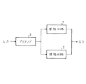
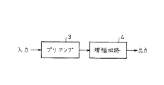
本実施例の信号増幅器は、入力信号をほぼ線形増幅するプリアンプ3と、プリアンプ3からの出力をほぼ線形増幅する増幅回路1、2(第1、第2の増幅回路)とを備えており、増幅回路1、2は並列接続されている。
【0022】
増幅回路1における、プリアンプ3からの出力のレベルが増大するレベル変化に対するスルー・レート(応答速度)は、増幅回路2におけるそのスルー・レートよりも大きく設定されており、増幅回路2における、プリアンプ3からの出力のレベルが減少するレベル変化に対するスルー・レートは、増幅回路1におけるそのスルー・レートよりも大きく設定されている。
【0023】
上記の構成において、プリアンプ3は入力信号を所定のレベルまで線形増幅する。プリアンプ3からの出力は、増幅回路1、2に入力される。増幅回路1、2は、プリアンプ3からの出力を線形増幅する。そして、信号増幅器は、増幅回路1の出力と増幅回路2の出力との和を出力信号として出力する。
【0024】
プリアンプ3からの出力のレベルが増大するレベル変化があったとき、換言すれば、入力信号のレベルが増大するレベル変化があったとき、増幅回路1は、そのレベル変化に高速応答した出力信号を出力する。一方、プリアンプ3からの出力のレベルが減少するレベル変化があったとき、換言すれば、入力信号のレベルが減少するレベル変化があったとき、増幅回路2は、そのレベル変化に高速応答した出力信号を出力する。つまり、本実施例の信号増幅器によれば、入力信号のレベル変化に関わらず、入力信号に高速応答した出力を得ることができる。
【0025】
ところで、入力信号のレベルが減少するレベル変化に対する増幅回路1のスルー・レートおよび、入力信号のレベルが増大するレベル変化に対する増幅回路2のスルー・レートは、原理上、本実施例の信号増幅器のスルー・レートにほとんど影響を与えない。このため、増幅回路1では、入力信号のレベルが減少するレベル変化に対するスルー・レートを小さくすることが可能であり、増幅回路2では、入力信号のレベルが増大するレベル変化に対するスルー・レートを小さくすることが可能である。
【0026】
それゆえ、これらのスルー・レートを小さくすることにより定常電流が小さくなる増幅回路1、2を採用すれば、応答速度が速く、しかも、消費電力が小さい信号増幅器を実現できる。
【0027】
増幅回路1、2の一参考例を、それぞれ、図2(a)、(b)に示す。
【0028】
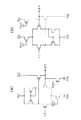
図2(a)は、2個の同極性のMOS型電界効果トランジスター、すなわち、nチャンネル型トランジスターTRN1、TRN2を電源VCCとVSSとの間に直列に接続したカスコード型線形回路である。電源VSS側のトランジスターTRN2は飽和領域で動作するように、定電圧Vbnがゲート電極に印加されている。入力信号はトランジスターTRN1のゲート電極に印加され、出力信号はトランジスターTRN1、TRN2の接続点から取り出される。
【0029】
図2(b)は、2個の同極性のMOS型電界効果トランジスター、すなわち、pチャンネル型トランジスターTRP1、TRP2を電源VCCとVSSとの間に直列に接続したカスコード型線形回路である。電源VCC側のトランジスターTRP2は飽和領域で動作するように、定電圧Vbpがゲート電極に印加されている。入力信号はトランジスターTRP1のゲート電極に印加され、出力信号はトランジスターTRP1、TRN2の接続点から取り出される。
【0030】
これらの回路では、いずれも、出力信号は、入力信号に対して線形ではあるが、一定のオフセットを有する。オフセット量は、定電流源として動作するトランジスターTRN2(TRP2)のゲート電極とソース電極との電位差に一致する。
【0031】
したがって、出力電圧は、nチャンネル型トランジスターTRN1、TRN2を用いた図2(a)の回路では、
Vout=Vin−(Vbn−Vcc)
となり、pチャンネル型トランジスターTRP1、TRP2を用いた図2(b)の回路では、
Vout=Vin−(Vbp−Vss)
となる。ここで、Vin、Voutは、それぞれ、入力電圧、出力電圧であり、Vcc、Vssは、それぞれ、電源VCC、VSSの電圧である。
【0032】
増幅回路1、2の他の参考例を、それぞれ、図3(a)、(b)に示す。なお、増幅回路1、2は、上記の特性を有しておれば、いかなる回路であってもよい。
【0033】
さらに、増幅回路1、2の具体例はそれぞれ単独の線形回路からなるのではなく、複数の線形回路の組み合わせからなる。
【0034】
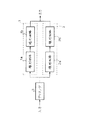
例えば、図4に示すように、増幅回路1を2個の直列接続した線形回路1a、1b(第1、第2の線形回路)で構成し、増幅回路2を2個の直列接続した線形回路2a、2b(第3、第4の線形回路)で構成する。
【0035】
終段の線形回路1bにおける、入力レベルが増大するレベル変化に対するスルー・レートは、終段の線形回路2bにおけるそのスルー・レートよりも大きく設定されており、線形回路2bにおける、入力のレベルが減少するレベル変化に対するスルー・レートは、線形回路1bにおけるそのスルー・レートよりも大きく設定されている。
【0036】
プリアンプ3からの出力は、増幅回路1の線形回路1aと、増幅回路2の線形回路2aとに入力される。そして、線形回路1aの出力は線形回路1bに入力され、線形回路2aの出力は線形回路2bに入力される。そして、増幅回路1の出力と増幅回路2の出力との和が出力信号として出力される。
【0037】
プリアンプ3からの出力のレベルが増大するレベル変化があったとき、換言すれば、入力信号のレベルが増大するレベル変化があったとき、線形回路1bは、そのレベル変化に高速応答した出力信号を出力する。一方、プリアンプ3からの出力のレベルが減少するレベル変化があったとき、換言すれば、入力信号のレベルが減少するレベル変化があったとき、線形回路2bは、そのレベル変化に高速応答した出力信号を出力する。つまり、本実施例の信号増幅器によれば、入力信号のレベル変化に関わらず、入力信号に高速応答した出力を得ることができる。
【0038】
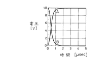
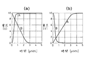
線形回路1b、2bに、それぞれ、上述のnチャンネル型トランジスターからなるカスコード型線形回路(図2(a))、pチャンネル型トランジスターからなるカスコード型線形回路(図2(b))を使用した場合の信号増幅器の応答性を図5に示す。
【0039】
曲線A、Bは、それぞれ、レベルが階段状に増大、減少するレベル変化を示す信号をプリアンプ3に入力したときに得られた出力信号である。いずれのレベル変化に対しても出力電圧が短時間で急激に増大、減少していることが分かる。つまり、いずれのレベル変化に対しても、高速応答している。
【0040】
比較のために、線形回路1b、2bの両方に同一極性のトランジスターからなるカスコード型線形回路を使用したときの信号増幅器の応答性を図6に示す。
【0041】
nチャンネル型トランジスターからなるカスコード型線形回路を使用した場合、同図(a)に示すように、レベルが階段状に増大するレベル変化を示す入力信号に対して応答速度が速いが、レベルが階段状に減少するレベル変化を示す入力信号に対して応答速度が遅いことが分かる。また、pチャンネル型トランジスターからなるカスコード型線形回路を使用した場合、同図(b)に示すように、レベルが階段状に減少するレベル変化を示す入力信号に対して応答速度が速いが、レベルが階段状に増大するレベル変化を示す入力信号に対して応答速度が遅いことが分かる。
【0042】
ところで、入力信号のレベルが減少するレベル変化に対する線形回路1bのスルー・レートおよび、入力信号のレベルが増大するレベル変化に対する線形回路2bのスルー・レートは、原理上、本実施例の信号増幅器のスルー・レートにほとんど影響を与えない。このため、線形回路1bでは、入力信号のレベルが減少するレベル変化に対するスルー・レートを小さくすることが可能であり、線形回路2bでは、入力信号のレベルが増大するレベル変化に対するスルー・レートを小さくすることが可能である。
【0043】
それゆえ、これらのスルー・レートを小さくすることにより定常電流が小さくなる線形回路1b、2bを採用すれば、応答速度が速く、しかも、消費電力が小さい信号増幅器を実現できる。
【0044】
なお、プリアンプ3の出力負荷は、線形回路1aおよび2aの入力容量だけであり、線形回路1a、2aの出力負荷は、それぞれ、線形回路1b、2bの入力容量だけである。このため、プリアンプ3および線形回路1a、2aの駆動力は小さくてもよい。したがって、定常電流が小さいプリアンプ3および線形回路1a、2aを採用することが可能であり、これにより、消費電力をさらに抑えることができる。
【0045】
以上のように、本実施例の信号増幅器によれば、消費電力を抑えることが可能であるので、多結晶シリコン薄膜あるいは単結晶シリコン薄膜に形成されたトランジスターのように、駆動能力の小さいトランジスターを採用することが可能である。これにより、応答速度の速い信号増幅器をローコストで実現できる。
【0046】
さらに、線形回路1a、2aに、それぞれ、線形回路1b、2bとは逆極性のトランジスターからなるカスコード型線形回路、すなわち、線形回路1aにpチャンネル型トランジスターからなるカスコード型線形回路、線形回路2aにnチャンネル型トランジスターからなるカスコード型線形回路を使用すれば、増幅回路1のオフセットと、増幅回路2のオフセットとを一致させることができる。このため、増幅回路1の出力レベルと増幅回路2の出力レベルとが一致するので、増幅回路1、2の出力間の干渉が起こりにくくなる。その結果、入力信号に対する線形性がより優れた出力を得ることができる。
【0047】
本発明の参考例について図7に基づいて説明すれば、以下の通りである。なお、説明の便宜上、前記の実施例の図面に示した部材と同一の機能を有する部材には、同一の符号を付記し、その説明を省略する。
【0048】
本参考例の信号増幅器は、入力信号をほぼ線形増幅するプリアンプ3と、プリアンプ3(増幅回路)からの出力をほぼ線形増幅し出力する増幅回路4とを備えている。プリアンプ3および増幅回路4には、具体的には例えば、前述のカスコード型線形回路(図2)が用いられる。
【0049】
増幅回路4は、シリコン薄膜に形成されたnチャンネル型トランジスター、pチャンネル型トランジスターの内、チャンネル幅当たりのコンダクタンスが大きい方のトランジスターからなっている。例えば、nチャンネル型トランジスターよりもpチャンネル型トランジスターの方が、チャンネル幅当たりのコンダクタンスが大きい場合、プリアンプ3には、nチャンネル型トランジスターからなるカスコード型線形回路を採用し、増幅回路4には、pチャンネル型トランジスターからなるカスコード型線形回路を採用する。
【0050】
これによれば、増幅回路4におけるトランジスターの単位面積当たりの駆動力が大きくなる。したがって、トランジスターの占有面積が同じ場合、従来よりも高速応答が可能となる。つまり、応答速度が速く、しかも、占有面積が小さい信号増幅器を実現できる。
【0051】
なお、増幅回路4はそれぞれ単独の線形回路からなる必要はなく、複数の線形回路を組み合わせてもよい。この場合、終段の線形回路にチャンネル幅当たりのコンダクタンスが大きい方のトランジスターを採用すればよい。
【0052】
一般には、pチャンネル型トランジスターよりもnチャンネル型トランジスターの方がキャリア移動度が大きいため、チャンネル幅当たりのコンダクタンスも大きいが、トランジスターの構造やトランジスターの製造条件によっては、逆の場合もある。
【0053】
例えば、絶縁基板上の多結晶シリコン薄膜に形成したトランジスターの場合、閾値電圧が、nチャンネル型トランジスターとpチャンネル型トランジスターとでは、大きく相違することがある。また、トランジスターの構造が同じであっても、ソース・ドレイン間耐圧が、nチャンネル型トランジスターとpチャンネル型トランジスターとでは、大きく相違することがある。これらの相違をできるだけ小さくするために、オフセット構造、または、LDD(Lightly Doped Drain)構造を採用した場合、実効的なキャリア移動度が低下するので、チャンネル幅当たりのコンダクタンスは、nチャンネル型トランジスターよりもpチャンネル型トランジスターの方が大きくなることがある。
【0054】
このような場合、増幅回路4の終段には、nチャンネル型トランジスターで構成されたカスコード型線形回路を採用するよりも、むしろ、チャンネル幅当たりのコンダクタンスが大きい方のトランジスターで構成された線形回路を採用することが有効である。
【0055】
次に、上記の信号増幅器の一応用例として、上記の信号増幅器を使用したアクティブ・マトリクス型画像表示装置について図8ないし図10に基づいて説明すれば、以下の通りである。
【0056】
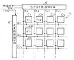
アクティブ・マトリクス型画像表示装置は、図8に示すように、画素アレイ11と、データ信号線SL1 、SL2 …を駆動するデータ信号線駆動回路12と、走査信号線GL1 、GL2 …を駆動する走査信号線駆動回路13とからなっている。画素アレイ11には、画素としてのセルCijがマトリクス状に設けられている。
【0057】
データ信号線駆動回路12は、タイミング信号TIM1に同期して、映像信号をサンプリングし、サンプリングにより得られたデータを必要に応じて増幅して、データ信号線SL1 、SL2 …に書き込む働きをする。走査信号線駆動回路13は、タイミング信号TIM2に同期して、走査信号線GL1 、GL2 …を順次選択する。
【0058】
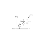
各セルCijの等価回路は、液晶表示装置の場合、図9に示すように、FET(電界効果トランジスター)等のスイッチング素子SWと、液晶容量Clと、必要に応じて液晶容量Clに並列に設けれる補助容量Csとからなっている。
【0059】
スイッチング素子SWのゲート、ドレインは、それぞれ、走査信号線GLi 、データ信号線SLj に接続されている。液晶容量Clの一方の電極はスイッチング素子SWのソースに接続されており、液晶容量Clの他方の電極(対向電極)は、全セルCijに共通の共通電極線に接続されている。
【0060】
走査信号線駆動回路13が走査信号線GLi を選択すると、スイッチング素子SWがオンになる。これにより、データ信号線SLj のデータが、スイッチング素子SWのドレイン、ソースを介して液晶容量Clに送られる。液晶容量Clはデータを保持する。そして、液晶容量Clに印加された電圧に応じて、液晶の透過率または反射率が変調され、その結果、画像が表示される。
【0061】
データ信号線駆動回路12でデータ信号線SL1 、SL2 …を駆動する方式には、アナログ方式とディジタル方式とがある。多階調表示を行う場合、アナログ方式の方が優れている。
【0062】
アナログ方式で線順次駆動方式のデータ信号線駆動回路12は、図10に示すように、スタートパルスSRTによりトリガーされ、クロック信号CLKに基づいてパルスNj を出力するシフトレジスターSRを備えている。アナログ・スイッチASjは、パルスNj に同期して開閉する。これにより、映像信号線SIGの映像信号がサンプリングされ、一旦、データとしてサンプリング容量Csajに蓄えられる。そして、次の水平帰線期間に、転送信号線TRFの転送信号によりアナログ・スイッチBSjを開閉させる。これにより、サンプリング容量Csajに蓄えたデータをホールド容量Chjへ転送すると共に、次の水平走査期間にデータを信号増幅器AMPjを介してデータ信号線SLj に出力する。
【0063】
ここで、j=1,2,…,mであり、mは横方向の画素数である。なお、必要に応じて、パルスNj の増幅および位相反転等を行うサンプリング回路SMPjが付加される。
【0064】
以上のように、線順次駆動方式の場合、ある水平走査期間にアナログスイッチASjでサンプリングしたデータを、次の水平走査期間にデータ信号線SLj に出力しているので、サンプリングしたデータを、同じ水平走査期間内に出力する点順次駆動方式の場合と比較して、データの書き込み時間を充分に確保することができる。その結果、表示品位に優れた画像が得られる。
【0065】
上記の信号増幅器AMPjとして、高速応答性を有する本実施例の信号増幅器を採用すれば、さらに、データの書き込み時間に余裕が生まれる。このため、データの書き込み時間が少ない高精細の画像表示装置や大画面の画像表示装置にも充分対応できる。
【0066】
例えば、パーソナル・コンピューター等で採用されているVGA(ビデオ・グラフィク・アレイ)規格では、約30μsec以内にデータを書き込む必要がある。また、画像表示装置として、25cm(10型)相当の液晶パネルを使用した場合、負荷は数十pF以上にも達する。このように、短時間で大容量の負荷を駆動する場合でも、本実施例の信号増幅器によれば、充分対応できる。
【0067】
特に、近年、開発が進められているモノリシック構造(画素アレイと駆動回路とが同一基板上に一体形成された構造)の液晶表示装置においては、駆動回路12の素子として、特性(キャリア移動度や閾値電圧、耐圧など)の劣った薄膜トランジスターを用いることになるが、本実施例の信号増幅器によれば、充分対応できる。
【0068】
また、上記モノリシック構造の液晶表示装置の大型化のために、基板として安価なガラス基板を用いた場合には、その歪み点(約600℃)以下の温度で素子を製造する必要があるが、そのようなプロセスで製造された素子は、特性がさらに劣っているが、本実施例の信号増幅器によれば、充分対応できる。
【0069】
さらに、ガラス基板上に前述したようなデータ信号線駆動回路12を形成し、該基板を、画素アレイ11を構成した基板上に実装する場合にも、本実施例の信号増幅器によれば、充分対応できる。
【0070】
上記実施例では、信号増幅器の応用例として、アクティブ・マトリクス型液晶表示装置を中心に記述したが、本発明は、これに限らず、他のアクティブ・マトリクス型画像表示装置、あるいは、その他のシステムにも適用できる。
【0071】
【発明の効果】
請求項1の発明に係る信号増幅器は、以上のように、互いに並列接続され、それぞれ入力信号を線形増幅する第1、第2の増幅回路が設けられており、入力信号のレベルが増大するレベル変化に対する応答速度は、第1の増幅回路の方が第2の増幅回路よりも大きくなるように設定されており、入力信号のレベルが減少するレベル変化に対する応答速度は、第2の増幅回路の方が第1の増幅回路よりも大きくなるように設定されおり、前記の第1の増幅回路は、入力信号を線形増幅するpチャンネル型トランジスターからなる第1の線形回路と、第1の線形回路の出力信号を線形増幅するnチャンネル型トランジスターからなる第2の線形回路とを含んでおり、前記の第2の増幅回路は、入力信号を線形増幅するnチャンネル型トランジスターからなる第3の線形回路と、第3の線形回路の出力信号を線形増幅するpチャンネル型トランジスターからなる第4の線形回路とを含んでいる構成である。
【0072】
これによれば、入力信号を線形増幅できる。しかも、入力信号のレベルが増大するレベル変化があったとき、そのレベル変化に高速応答した出力が第1の増幅回路から得られ、入力信号のレベルが減少するレベル変化があったとき、そのレベル変化に高速応答した出力が第2の増幅回路から得られる。つまり、入力信号のレベル変化に関わらず、入力信号に高速応答した出力を得ることができるという効果を奏する。
【0073】
これに加え、第1の増幅回路と第2の増幅回路とがトランジスターのチャンネル極性について対称になる。このため、第1の増幅回路で生じるオフセットと第2の増幅回路で生じるオフセットとが同一になる。換言すれば、第1の増幅回路からの出力のレベルと第2の増幅回路からの出力のレベルとを一致させることができる。これにより、第1の増幅回路からの出力と第2の増幅回路からの出力とが干渉しにくくなるので、入力信号に対する線形性がより高い出力を得ることができるという効果を奏する。
【0074】
請求項2の発明に係る信号増幅器は、以上のように、請求項1の信号増幅器であって、前記の第1、第2の増幅回路が、シリコン薄膜に形成されている構成である。
【0075】
これによれば、請求項1の効果に加え、応答速度の速い信号増幅器をローコストで実現できるという効果を奏する。
【0076】
請求項3の発明に係る画像表示装置は、以上のように、マトリクス状に配置された複数の表示素子と、映像信号をデータ信号線に出力するデータ信号線駆動回路と、走査信号を走査信号線に出力する走査信号線駆動回路と、表示素子毎に設けられ、データ信号線上の映像信号を走査信号線上の走査信号に応じて表示素子に出力するスイッチング素子とが備えられており、上記のデータ信号線駆動回路は、映像信号を線形増幅しデータ信号線に出力する信号増幅器として、請求項1または2に記載の信号増幅器を含んでいる構成である。
【0077】
これによれば、データ信号線駆動回路の信号増幅器に上記の応答速度の速い信号増幅器を採用したので、映像信号をデータ信号線に短時間で出力することができる。これにより、動作周波数が高い画像表示装置、つまり、高品位画像を表示できる画像表示装置を実現することが可能になるという効果を奏する。
【図面の簡単な説明】
【図1】 本発明に係る信号増幅器の構成を示すブロック図である。
【図2】 図1の信号増幅器における増幅回路の参考例を示す回路図である
【図3】 図1の信号増幅器における増幅回路の他の参考例を示す回路図である
【図4】 図1の信号増幅器の具体例を示すブロック図である。
【図5】 図1および図4の信号増幅器の応答性を示すグラフである。
【図6】 比較例を示すものであり、信号増幅器の応答性を示すグラフである。
【図7】 参考例の信号増幅器の構成を示すブロック図である。
【図8】 本発明に係る信号増幅器の応用例を示すものであり、アクティブ・マトリクス型画像表示装置の概略の構成を示すブロック図である。
【図9】 図8のアクティブ・マトリクス型画像表示装置としての液晶表示装置において、セルの等価回路図である
【図10】 図8のアクティブ・マトリクス型画像表示装置におけるデータ信号線の駆動回路を示すブロック図である。
【図11】 従来の信号増幅器を示す回路図である。
【符号の説明】
1 増幅回路(第1の増幅回路)
1a 線形回路(第1の線形回路)
1b 線形回路(第2の線形回路)
2 増幅回路(第2の増幅回路)
2a 線形回路(第3の線形回路)
2b 線形回路(第4の線形回路)
3 プリアンプ(増幅回路)
4 増幅回路
11 画素アレイ
12 データ信号線駆動回路
13 走査信号線駆動回路
AMP 信号増幅器[0001]
[Industrial application fields]
The present invention relates to a signal amplifier capable of obtaining an output proportional to an input, and an image display apparatus using the signal amplifier.
[0002]
[Prior art]
As a signal amplifier having a linear characteristic that an output proportional to the input can be obtained, an operational amplifier is usually used. However, a cascode amplifier requiring a small number of elements is often used.
[0003]
The cascode amplifier is described in, for example, “Electronic Circuit for Transistors and ICs (II) 2nd Edition” published on July 10, 1982 by McGraw-Hill Book, p. As described in H.324, two bipolar transistors of the same kind are connected in series, and the DC level differs between the output and input, but the AC component does not attenuate. Yes.
[0004]
An example of a signal amplifier using a cascode amplifier is shown in FIG.
[0005]
This signal amplifier includes two cascode amplifiers connected in series. The front-stage cascode amplifier is composed of p-channel transistors TRP1 and TRP2 connected in series between the power supplies VCC and VSS, and the rear-stage cascode amplifier is connected in series between the power supplies VCC and VSS. It consists of n-channel transistors TRN1 and TRN2. Predetermined voltages Vbp and Vbn are applied to the gates of the transistors TRP2 and TRN2, respectively, so as to function as constant current sources. The input signal is applied to the gate electrode of the transistor TRP1, and the output signal is taken out from the connection point of the transistors TRN1 and TRN2.
[0006]
As described above, by providing two cascode amplifiers in series, fluctuations in the output level do not affect the input level.
[0007]
Since the above-described signal amplifier has a characteristic that an output proportional to the input can be obtained, it is used in various fields. For example, in the field of active matrix type image display devices, it is used for a signal amplifier in a data signal line driving circuit for writing a video signal to a data signal line.
[0008]
[Problems to be solved by the invention]
However, in the conventional signal amplifier, when there is a level change in which the level of the input signal increases, an output that responds quickly to the level change is obtained, but when there is a level change in which the level of the input signal decreases, There is a problem that an output that responds quickly to the level change cannot be obtained.
[0009]
For this reason, when the signal amplifier is used in an active matrix image display device, there is a possibility that the video signal cannot be written to the data signal line within a predetermined period. In particular, when used in an image display apparatus that performs multi-gradation display, the display quality is likely to deteriorate.
[0010]
If the driving capability of the transistor TRN2 is increased (that is, if the steady current in the transistor TRN2 is increased), even if there is a level change in which the level of the input signal decreases, an output that responds quickly to the level change can be obtained. However, if the driving capability of the transistor TRN2 is increased, a new problem of increasing power consumption is caused.
[0011]
In particular, a transistor formed on a polycrystalline silicon thin film on an insulating substrate has lower carrier mobility, a higher threshold voltage, and a lower breakdown voltage than a transistor formed on a single crystal silicon substrate. It is difficult to increase the driving capability beyond a certain level.
[0012]
Therefore, to achieve an active matrix image display device in which a pixel array and a drive circuit are monolithically formed on a polycrystalline silicon thin film on an insulating substrate in order to increase the screen and reduce costs, conventional signal amplifiers do not. There is a problem that it is difficult to realize.
[0013]
[Means for Solving the Problems]
In order to solve the above problems, signal amplifiers according to the invention of
[0014]
Claim2In order to solve the above problems, a signal amplifier according to the present invention is1The first and second amplifier circuits are formed in a silicon thin film.
[0015]
In order to solve the above problems, an image display device according to a third aspect of the present invention includes a plurality of display elements arranged in a matrix, a data signal line driving circuit for outputting a video signal to a data signal line, and scanning. A scanning signal line driving circuit that outputs a signal to the scanning signal line, and a switching element that is provided for each display element and outputs a video signal on the data signal line to the display element according to the scanning signal on the scanning signal line are provided. The data signal line driving circuit described abovelineThe signal amplifier according to
[0016]
[Action]
According to the configuration of the first aspect, the input signal can be linearly amplified. Moreover, when there is a level change that increases the level of the input signal, an output that responds quickly to the level change is obtained from the first amplifier circuit, and when there is a level change that decreases the level of the input signal, that level. An output that responds quickly to the change is obtained from the second amplifier circuit. In other words, an output that responds quickly to the input signal can be obtained regardless of the level change of the input signal.
[0017]
thisIn addition, the first amplifier circuit and the second amplifier circuit are symmetric with respect to the channel polarity of the transistor. For this reason, the offset generated in the first amplifier circuit is the same as the offset generated in the second amplifier circuit. In other words, the output level from the first amplifier circuit can be matched with the output level from the second amplifier circuit. This makes it difficult for the output from the first amplifier circuit and the output from the second amplifier circuit to interfere with each other, so that an output with better linearity with respect to the input signal can be obtained.
[0018]
Claim2According to the structure of claim1In addition to the above operation, a signal amplifier having a high response speed can be realized at low cost.
[0019]
Claim3With this configuration, since the signal amplifier having a high response speed is employed as the signal amplifier of the data signal line driving circuit, the video signal can be output to the data signal line in a short time. This makes it possible to realize an image display device with a high operating frequency, that is, an image display device capable of displaying a high-quality image.
[0020]
【Example】
An embodiment of the present invention will be described with reference to FIGS. 1 to 6 as follows.
[0021]
The signal amplifier according to the present embodiment includes a
[0022]
A slew rate (response speed) with respect to a level change in the
[0023]
In the above configuration, the
[0024]
When there is a level change that increases the level of the output from the
[0025]
By the way, the slew rate of the
[0026]
Therefore, if the
[0027]
One of
[0028]
FIG. 2A shows a cascode linear circuit in which two MOS field effect transistors having the same polarity, that is, n-channel transistors TRN1 and TRN2 are connected in series between power supplies VCC and VSS. The constant voltage Vbn is applied to the gate electrode so that the transistor TRN2 on the power supply VSS side operates in the saturation region. The input signal is applied to the gate electrode of the transistor TRN1, and the output signal is taken out from the connection point of the transistors TRN1 and TRN2.
[0029]
FIG. 2B shows a cascode linear circuit in which two MOS field effect transistors having the same polarity, that is, p-channel transistors TRP1 and TRP2 are connected in series between power supplies VCC and VSS. The constant voltage Vbp is applied to the gate electrode so that the transistor TRP2 on the power supply VCC side operates in the saturation region. The input signal is applied to the gate electrode of the transistor TRP1, and the output signal is taken out from the connection point of the transistors TRP1 and TRN2.
[0030]
In any of these circuits, the output signal is linear with respect to the input signal, but has a constant offset. The offset amount matches the potential difference between the gate electrode and the source electrode of the transistor TRN2 (TRP2) operating as a constant current source.
[0031]
Therefore, in the circuit of FIG. 2A using the n-channel transistors TRN1 and TRN2, the output voltage is
Vout = Vin− (Vbn−Vcc)
In the circuit of FIG. 2B using the p-channel type transistors TRP1 and TRP2,
Vout = Vin− (Vbp−Vss)
It becomes. Here, Vin and Vout are the input voltage and the output voltage, respectively, and Vcc and Vss are the voltages of the power supplies VCC and VSS, respectively.
[0032]
[0033]
Further, the
[0034]
For example, as shown in FIG. 4, the
[0035]
The slew rate with respect to the level change in which the input level increases in the final stage
[0036]
The output from the
[0037]
When there is a level change that increases the level of the output from the
[0038]
When the cascode linear circuit (FIG. 2 (a)) composed of the above-mentioned n-channel transistors and the cascode linear circuit (FIG. 2 (b)) composed of p-channel transistors are used for the
[0039]
Curves A and B are output signals obtained when a signal indicating a level change in which the level increases or decreases stepwise is input to the
[0040]
For comparison, FIG. 6 shows the responsiveness of a signal amplifier when a cascode linear circuit composed of transistors having the same polarity is used for both
[0041]
When a cascode linear circuit composed of n-channel transistors is used, the response speed is fast for an input signal showing a level change in which the level increases stepwise as shown in FIG. It can be seen that the response speed is slow with respect to an input signal showing a level change that decreases in a manner. Also, when a cascode linear circuit composed of p-channel transistors is used, the response speed is fast with respect to an input signal indicating a level change in which the level decreases stepwise as shown in FIG. It can be seen that the response speed is slow with respect to an input signal showing a level change that increases in a stepwise manner.
[0042]
By the way, the slew rate of the
[0043]
Therefore, if the
[0044]
The output load of the
[0045]
As described above, according to the signal amplifier of this embodiment, it is possible to reduce power consumption. Therefore, a transistor having a low driving capability such as a transistor formed on a polycrystalline silicon thin film or a single crystal silicon thin film can be used. It is possible to adopt. Thereby, a signal amplifier having a high response speed can be realized at low cost.
[0046]
Further, the
[0047]
The present inventionNounAn example will be described with reference to FIG. For convenience of explanation, members having the same functions as those shown in the drawings of the above-described embodiment are denoted by the same reference numerals and description thereof is omitted.
[0048]
The signal amplifier of this reference example includes a
[0049]
The
[0050]
This increases the driving force per unit area of the transistor in the
[0051]
The
[0052]
In general, an n-channel transistor has a higher carrier mobility than a p-channel transistor, and therefore conductance per channel width is large. However, the reverse may occur depending on the transistor structure and transistor manufacturing conditions.
[0053]
For example, in the case of a transistor formed on a polycrystalline silicon thin film on an insulating substrate, the threshold voltage may be greatly different between an n-channel transistor and a p-channel transistor. Even if the transistor structure is the same, the source-drain breakdown voltage may be greatly different between an n-channel transistor and a p-channel transistor. In order to make these differences as small as possible, when an offset structure or LDD (Lightly Doped Drain) structure is adopted, the effective carrier mobility is lowered, so the conductance per channel width is smaller than that of an n-channel transistor. However, the p-channel transistor may be larger.
[0054]
In such a case, rather than adopting a cascode linear circuit composed of n-channel transistors at the final stage of the
[0055]
Next, as an application example of the signal amplifier, an active matrix image display device using the signal amplifier will be described with reference to FIGS.
[0056]
As shown in FIG. 8, the active matrix type image display device includes a
[0057]
The data signal
[0058]
Each cell CijIn the case of a liquid crystal display device, as shown in FIG. 9, the equivalent circuit is a switching element SW such as an FET (field effect transistor), a liquid crystal capacitor Cl, and an auxiliary capacitor provided in parallel with the liquid crystal capacitor Cl as necessary. It consists of Cs.
[0059]
The gate and drain of the switching element SW are respectively connected to the scanning signal line GL.i, Data signal line SLjIt is connected to the. One electrode of the liquid crystal capacitor Cl is connected to the source of the switching element SW, and the other electrode (counter electrode) of the liquid crystal capacitor Cl is connected to the entire cell C.ijAre connected to a common electrode line.
[0060]
The scanning signal
[0061]
Data signal line SL in data signal
[0062]
As shown in FIG. 10, the data signal
[0063]
Here, j = 1, 2,..., M, and m is the number of pixels in the horizontal direction. If necessary, pulse NjA sampling circuit SMPj for performing amplification and phase inversion is added.
[0064]
As described above, in the case of the line sequential driving method, data sampled by the analog switch ASj in a certain horizontal scanning period is converted into the data signal line SL in the next horizontal scanning period.jAs compared with the case of the dot sequential driving method in which sampled data is output within the same horizontal scanning period, a sufficient data writing time can be secured. As a result, an image excellent in display quality can be obtained.
[0065]
If the signal amplifier of this embodiment having a high-speed response is employed as the signal amplifier AMPj, there is a margin in data writing time. For this reason, it can sufficiently cope with a high-definition image display device or a large-screen image display device with a short data writing time.
[0066]
For example, in the VGA (Video Graphics Array) standard adopted in personal computers and the like, it is necessary to write data within about 30 μsec. Further, when a liquid crystal panel equivalent to 25 cm (10 type) is used as the image display device, the load reaches several tens of pF or more. Thus, even when a large-capacity load is driven in a short time, the signal amplifier of this embodiment can sufficiently cope with it.
[0067]
In particular, in a liquid crystal display device having a monolithic structure (a structure in which a pixel array and a drive circuit are integrally formed on the same substrate) that are being developed in recent years, characteristics (carrier mobility, Although a thin film transistor having a poor threshold voltage, withstand voltage, etc. is used, the signal amplifier of this embodiment can sufficiently cope with it.
[0068]
In addition, when an inexpensive glass substrate is used as a substrate for increasing the size of the liquid crystal display device having the monolithic structure, it is necessary to manufacture an element at a temperature equal to or lower than the strain point (about 600 ° C.). The element manufactured by such a process is further inferior in characteristics, but the signal amplifier of this embodiment can sufficiently cope with it.
[0069]
Further, when the data signal
[0070]
In the above embodiment, the active matrix type liquid crystal display device is mainly described as an application example of the signal amplifier. However, the present invention is not limited to this, and other active matrix type image display devices or other systems are described. It can also be applied to.
[0071]
【The invention's effect】
The signal amplifiers according to the invention of
[0072]
According to this, the input signal can be linearly amplified. Moreover, when there is a level change that increases the level of the input signal, an output that responds quickly to the level change is obtained from the first amplifier circuit, and when there is a level change that decreases the level of the input signal, that level. An output that responds quickly to the change is obtained from the second amplifier circuit. That is, there is an effect that an output that responds to the input signal at high speed can be obtained regardless of the level change of the input signal.
[0073]
thisIn additionIn other words, the first amplifier circuit and the second amplifier circuit are symmetric with respect to the channel polarity of the transistor. For this reason, the offset generated in the first amplifier circuit is the same as the offset generated in the second amplifier circuit. In other words, the output level from the first amplifier circuit can be matched with the output level from the second amplifier circuit. As a result, the output from the first amplifier circuit and the output from the second amplifier circuit are less likely to interfere with each other, so that an output with higher linearity with respect to the input signal can be obtained.
[0074]
Claim2The signal amplifier according to the present invention is as described above.1In this signal amplifier, the first and second amplifier circuits are formed in a silicon thin film.
[0075]
According to this, the claim1In addition to the above effect, a signal amplifier having a high response speed can be realized at a low cost.
[0076]
As described above, the image display device according to the third aspect of the present invention includes a plurality of display elements arranged in a matrix, a data signal line driving circuit for outputting a video signal to a data signal line, and a scanning signal as a scanning signal. A scanning signal line driving circuit for outputting to the line, and a switching element provided for each display element and outputting the video signal on the data signal line to the display element in accordance with the scanning signal on the scanning signal line. The data signal line drive circuitlineThe signal amplifier according to
[0077]
According to this, since the signal amplifier having a high response speed is adopted as the signal amplifier of the data signal line driving circuit, the video signal can be output to the data signal line in a short time. As a result, it is possible to realize an image display device having a high operating frequency, that is, an image display device capable of displaying a high-quality image.
[Brief description of the drawings]
FIG. 1 is a block diagram showing a configuration of a signal amplifier according to the present invention.
2 is a diagram of an amplifier circuit in the signal amplifier of FIG.referenceIt is a circuit diagram which shows an example
FIG. 3 shows another amplifier circuit in the signal amplifier of FIG.referenceIt is a circuit diagram which shows an example
4 is a diagram of the signal amplifier of FIG.Concrete exampleFIG.
5 is a graph showing the responsiveness of the signal amplifier of FIGS. 1 and 4. FIG.
FIG. 6 is a graph showing a response example of a signal amplifier, showing a comparative example.
FIG. 7 is a block diagram showing a configuration of a signal amplifier of a reference example.
FIG. 8 is a block diagram showing a schematic configuration of an active matrix image display device, showing an application example of the signal amplifier according to the present invention.
9 is an equivalent circuit diagram of a cell in the liquid crystal display device as the active matrix image display device of FIG.
10 is a block diagram showing a data signal line drive circuit in the active matrix image display device of FIG. 8; FIG.
FIG. 11 is a circuit diagram showing a conventional signal amplifier.
[Explanation of symbols]
1. Amplifier circuit (first amplifier circuit)
1a linear circuit (first linear circuit)
1b Linear circuit (second linear circuit)
2 Amplifier circuit (second amplifier circuit)
2a Linear circuit (third linear circuit)
2b Linear circuit (fourth linear circuit)
3 Preamplifier (amplifier circuit)
4 Amplifier circuit
11 pixel array
12 Data signal line drive circuit
13 Scanning signal line drive circuit
AMP signal amplifier
Claims (3)
前記の第1の増幅回路は、入力信号を線形増幅するpチャンネル型トランジスターからなる第1の線形回路と、第1の線形回路の出力信号を線形増幅するnチャンネル型トランジスターからなる第2の線形回路とを含んでおり、前記の第2の増幅回路は、入力信号を線形増幅するnチャンネル型トランジスターからなる第3の線形回路と、第3の線形回路の出力信号を線形増幅するpチャンネル型トランジスターからなる第4の線形回路とを含んでいることを特徴とする信号増幅器。Connected in parallel to each other, the first line-type amplifying an input signal, respectively, provided the second amplifier circuit, the response speed against the change in level the level of the input signal is increased, the direction of the first amplifier circuit first The second amplifier circuit is set to be larger than the second amplifier circuit, and the response speed to the level change in which the level of the input signal decreases is set so that the second amplifier circuit is larger than the first amplifier circuit. And
First amplifying circuit of said, a first linear circuit composed of p-channel transistor which linear amplifying an input signal, a second consisting of n-channel transistor which linear amplifies the output signal of the first linear circuit of includes a linear circuit, a second amplifying circuit of the includes a third linear circuit composed of n-channel transistor which linear amplifying an input signal, linear output signal of the third linear circuit amplification And a fourth linear circuit comprising a p-channel transistor.
Priority Applications (4)
| Application Number | Priority Date | Filing Date | Title |
|---|---|---|---|
| JP11923894A JP3717536B2 (en) | 1994-05-31 | 1994-05-31 | Signal amplifier and image display device |
| CNB951023527A CN1136529C (en) | 1994-05-31 | 1995-03-22 | Sampling circuit, signal amplifier, and image display |
| KR1019950007883A KR950034028A (en) | 1994-05-31 | 1995-03-31 | Sampling circuit, signal amplifier and image display device |
| US09/594,439 US6225866B1 (en) | 1994-05-31 | 2000-06-14 | Series connected multi-stage linear FET amplifier circuit |
Applications Claiming Priority (1)
| Application Number | Priority Date | Filing Date | Title |
|---|---|---|---|
| JP11923894A JP3717536B2 (en) | 1994-05-31 | 1994-05-31 | Signal amplifier and image display device |
Publications (2)
| Publication Number | Publication Date |
|---|---|
| JPH07325555A JPH07325555A (en) | 1995-12-12 |
| JP3717536B2 true JP3717536B2 (en) | 2005-11-16 |
Family
ID=14756388
Family Applications (1)
| Application Number | Title | Priority Date | Filing Date |
|---|---|---|---|
| JP11923894A Expired - Fee Related JP3717536B2 (en) | 1994-05-31 | 1994-05-31 | Signal amplifier and image display device |
Country Status (1)
| Country | Link |
|---|---|
| JP (1) | JP3717536B2 (en) |
Families Citing this family (3)
| Publication number | Priority date | Publication date | Assignee | Title |
|---|---|---|---|---|
| JP3844613B2 (en) | 1998-04-28 | 2006-11-15 | 株式会社半導体エネルギー研究所 | Thin film transistor circuit and display device using the same |
| JP3880416B2 (en) | 2002-02-13 | 2007-02-14 | シャープ株式会社 | Active matrix substrate |
| JP5086010B2 (en) * | 2007-09-10 | 2012-11-28 | ラピスセミコンダクタ株式会社 | LCD panel drive circuit |
-
1994
- 1994-05-31 JP JP11923894A patent/JP3717536B2/en not_active Expired - Fee Related
Also Published As
| Publication number | Publication date |
|---|---|
| JPH07325555A (en) | 1995-12-12 |
Similar Documents
| Publication | Publication Date | Title |
|---|---|---|
| US6225866B1 (en) | Series connected multi-stage linear FET amplifier circuit | |
| US6313819B1 (en) | Liquid crystal display device | |
| KR0139697B1 (en) | Image display | |
| JP4275166B2 (en) | Data driver and display device | |
| KR100564275B1 (en) | LCD Display | |
| JP3144166B2 (en) | Low amplitude input level conversion circuit | |
| JP6007215B2 (en) | Semiconductor device | |
| US7903078B2 (en) | Data driver and display device | |
| JP2002041001A (en) | Image display device and driving method thereof | |
| US6970152B1 (en) | Stacked amplifier arrangement for graphics displays | |
| JPH021893A (en) | Display device line driver having automatically uniform compensation | |
| CN1383123A (en) | Source Driver Amplifiers for LCD Displays | |
| US7646371B2 (en) | Driver circuit, electro-optical device, and electronic instrument | |
| JP2005143068A (en) | Inverter circuit and display device | |
| US6275210B1 (en) | Liquid crystal display device and driver circuit thereof | |
| CN110047451A (en) | Source electrode driver, array substrate and liquid crystal display panel | |
| JPH08137443A (en) | Image display device | |
| JP3356580B2 (en) | Image display device | |
| US7221194B2 (en) | Analog buffers composed of thin film transistors | |
| US5952854A (en) | Sampling circuit and image display device | |
| US7106136B2 (en) | Amplifier, data driver and display apparatus having the same | |
| JP3201910B2 (en) | Buffer circuit and image display device | |
| JP3294057B2 (en) | Signal amplifier, signal line drive circuit, and image display device | |
| US6480179B1 (en) | Image display invention | |
| JP3717536B2 (en) | Signal amplifier and image display device |
Legal Events
| Date | Code | Title | Description |
|---|---|---|---|
| A521 | Written amendment |
Free format text: JAPANESE INTERMEDIATE CODE: A523 Effective date: 20050804 |
|
| RD02 | Notification of acceptance of power of attorney |
Free format text: JAPANESE INTERMEDIATE CODE: A7422 Effective date: 20050804 |
|
| A61 | First payment of annual fees (during grant procedure) |
Free format text: JAPANESE INTERMEDIATE CODE: A61 Effective date: 20050831 |
|
| R150 | Certificate of patent or registration of utility model |
Free format text: JAPANESE INTERMEDIATE CODE: R150 |
|
| FPAY | Renewal fee payment (event date is renewal date of database) |
Free format text: PAYMENT UNTIL: 20080909 Year of fee payment: 3 |
|
| FPAY | Renewal fee payment (event date is renewal date of database) |
Free format text: PAYMENT UNTIL: 20090909 Year of fee payment: 4 |
|
| FPAY | Renewal fee payment (event date is renewal date of database) |
Free format text: PAYMENT UNTIL: 20090909 Year of fee payment: 4 |
|
| FPAY | Renewal fee payment (event date is renewal date of database) |
Free format text: PAYMENT UNTIL: 20100909 Year of fee payment: 5 |
|
| FPAY | Renewal fee payment (event date is renewal date of database) |
Free format text: PAYMENT UNTIL: 20110909 Year of fee payment: 6 |
|
| LAPS | Cancellation because of no payment of annual fees |