JP3715784B2 - Image processing apparatus, image display apparatus, and computer-readable storage medium - Google Patents
Image processing apparatus, image display apparatus, and computer-readable storage medium Download PDFInfo
- Publication number
- JP3715784B2 JP3715784B2 JP14162998A JP14162998A JP3715784B2 JP 3715784 B2 JP3715784 B2 JP 3715784B2 JP 14162998 A JP14162998 A JP 14162998A JP 14162998 A JP14162998 A JP 14162998A JP 3715784 B2 JP3715784 B2 JP 3715784B2
- Authority
- JP
- Japan
- Prior art keywords
- data
- transmission signal
- signal
- image
- memory
- Prior art date
- Legal status (The legal status is an assumption and is not a legal conclusion. Google has not performed a legal analysis and makes no representation as to the accuracy of the status listed.)
- Expired - Fee Related
Links
Images


Description
【0001】
【発明の属する技術分野】
本発明は、画像処理装置、画像表示装置及びコンピュータ読み取り可能な記憶媒体に関するものであり、特に強誘電性液晶を用いた液晶表示器のような記憶性を有する表示装置を複数接続し、各々の液晶表示器に画像を表示すると共に、音声信号も伝送するシステムに用いて好適なものである。
【0002】
【従来の技術】
従来より、特願平7−013046号に開示される表示装置のように、メモリ効果を持つ強誘電性液晶を用いた複数台の液晶表示器(以下FLCD)を1台のホストコンピュータに接続し、各々のFLCDに同一もしくは各々異なる画像を表示する画像表示システムが提案されている。
【0003】
先ず、この画像表示システムについて説明する。
図8はシステム全体の接続図であり、同図において、1はホストコンピュータ、101、102、103、104はFLCD、201、202、203、204は分岐伝送ユニット、500、501、502、503は伝送ケーブル、511、512、513、514は分岐ケーブルであり、ホストコンピュータ1からは、アドレスデータを先頭にした16bit画像データがパラレルで伝送ケーブル500を通じて出力される。
【0004】
各分岐伝送ユニット201〜204は、それぞれ前段から伝送ケーブル500〜503を経て入力された16bit画像データをそのまま中継して後段の分岐伝送ユニットへ伝送ケーブル501〜503から出力する一方、各分岐伝送ユニットに設けられた不図示のアドレス設定SW(スイッチ)の設定値と16bit画像データの先頭に配置されたアドレス出力とを比較し、一致すれば各々分岐ケーブル511〜514へも16bit画像データを出力する。各FLCD201〜204はこの16bit画像データに基づいて表示面に画像を描画する。また、各FLCD201〜204はメモリ効果を有するため、新たに16bit画像データを受信し描画されるまでは、その直前の画像データを表示し続ける。
尚、図8では4段の分岐伝送ユニットとそれに対応する4台のFLCDが接続されているが、接続段数の制約は特にない。
【0005】
ここで、ホストコンピュータ1から出力される16bit画像データとその先頭アドレスについて説明する。図9は16bit画像データの配列をイメージ的に描いた図であり、DATA0〜DATA15の16本のデータと、CLK及びAHDLからなる18本の信号から成る。
AHDLは通常Lであり、データの先頭のみHとなり、その時DATA0〜DATA15はアドレスデータを出力する。つまり、AHDLはデータの先頭を示すだけでなく、DATA0〜DATA15が画像データでは無く、アドレスデータであることを示す信号でもある。
【0006】
DATA0〜DATA15に乗せられたアドレスデータの内下位11bitDATA0〜10はFLCD201〜204の走査線番号のアドレスを示すものであり、上位5bitDATA11〜15が先に説明した設定SWの設定値に相当するものである。また、先頭のアドレスデータに続いて1水平走査分の画像データが配置されている。
【0007】
各分岐伝送ユニット201〜204はAHDLがHとなった時、DATA11〜15のみを監視し、設定SWの設定値と一致しない場合は、FLCDへの分岐ケーブル511〜514のAHDLをマスクし、Lを出力する。これを受けたFLCDはAHDLがLであるためアドレスとは認識せず、従って、描画している画像の更新は行われず、DATA11〜15にいかなるデータが乗っていようと無視される。一方、後段への伝送ケーブル501〜503には、前段から入力された信号を何も加工せずそのまま出力する。
【0008】
また、各分岐伝送ユニット201〜204は、AHDLがHとなった時にDATA11〜15が設定SWの設定値と一致しているとみなした場合、FLCDへの分岐出力のAHDLをマスクせずそのまま出力する。これを受けたFLCDはAHDLのHを受け、画像データのスタートを認識して描画画像の更新が行われる。尚この時、後段への伝送ケーブル501〜503にも、前段から入力された信号を何も加工せずそのまま出力する。
【0009】
【発明が解決しようとする課題】
しかしながら従来の画像表示システムは画像を伝送するのみであり、音声については対応していなかった。
【0010】
従って、本発明は、音声信号を伝送可能にした画像表示システムを実現できるようにすることを目的とする。
【0011】
【課題を解決するための手段】
本発明による画像処理装置においては、IDデータと画像データと音声データとが所定の順序で配列されたデータ信号と、上記IDデータか上記画像、音声データかを判別するための判別信号とを含む伝送信号を受信する受信手段と、IDを設定するID設定手段と、上記受信した伝送信号中のIDデータと上記設定されたIDとを比較して両者が一致したことを検出する検出手段と、上記両者が一致しないとき上記受信した伝送信号中の判別信号をマスクするマスク手段と、上記判別信号がマスクされた伝送信号を送出する第1の伝送信号出力手段と、上記受信した伝送信号をそのまま送出する第2の伝送信号出力手段と、上記受信した伝送信号中の音声データを記憶するメモリ手段と、上記メモリ手段の書き込みと読み出しを上記受信した伝送信号中の判別信号に基づいて制御するメモリ制御手段と、上記メモリ手段から読み出された音声データを出力する音声出力手段とを設けている。
【0012】
本発明による画像処理装置においては、IDデータと画像データと音声データとが所定の順序で配列されたデータ信号と、上記IDデータか上記画像、音声データかを判別するための判別信号とを含む伝送信号を受信する受信手段と、IDを設定するID設定手段と、上記受信した伝送信号中のIDデータと上記設定されたIDとを比較して両者が一致したことを検出する検出手段と、上記両者が一致しないとき上記受信した伝送信号中の判別信号をマスクするマスク手段と、上記判別信号がマスクされた伝送信号を送出する第1の伝送信号出力手段と、上記受信した伝送信号をそのまま送出する第2の伝送信号出力手段と、上記受信した伝送信号中の音声データを記憶するメモリ手段と、上記メモリ手段の書き込みと読み出しを上記受信した伝送信号中の判別信号に基づいて制御するメモリ制御手段と、上記メモリ手段から読み出された音声データを出力する音声出力手段とを有する画像処理部と、上記第1の伝送出力手段から出力される上記伝送信号中の画像データを表示する表示部とを設けている。
【0013】
本発明による記憶媒体においては、IDデータと画像データと音声データとが所定の順序で配列されたデータ信号と、上記IDデータか上記画像、音声データかを判別するための判別信号とを含む伝送信号を受信する受信手順と、IDを設定するID設定手順と、上記受信した伝送信号中のIDデータと上記設定されたIDとを比較して両者が一致したことを検出する検出手順と、上記両者が一致しないとき上記受信した伝送信号中の判別信号をマスクするマスク手順と、上記判別信号がマスクされた伝送信号を送出する第1の伝送信号出力手順と、上記受信した伝送信号をそのまま送出する第2の伝送信号出力手順と、上記受信した伝送信号中の音声データをメモリ手段に記憶する記憶手順と、上記メモリ手段の書き込みと読み出しを上記受信した伝送信号中の判別信号に基づいて制御するメモリ制御手順と、上記記憶手順により読み出された音声データを出力する音声出力手順とをコンピュータに実行させるためのプログラムを記憶している。
【0014】
【発明の実施の形態】
(第1の実施の形態)
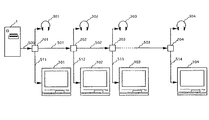
図1は本発明による画像表示装置としての画像表示システムの全体的な構成を示す図であり、図2は16bit伝送データの配列をイメージ的に示した図である。
図1において1はホストコンピュータ、101、102、103、104はFLCD、201、202、203、204は分岐伝送ユニット、301、302、303、304はヘッドホン、500、501、502、503は伝送ケーブル、511、512、513、514は分岐ケーブルである。
【0015】
ホストコンピュータ1からは、図2に示すようなIDアドレスデータが先頭で、それ以降は画像データである16bitデータ信号がパラレルで伝送ケーブル500から出力される。また、本発明による画像処理装置、画像処理部を構成し、信号を中継、分岐するための各分岐伝送ユニット201〜204は、前段の伝送ユニットあるいはホストコンピュータ1から入力された16bit伝送データ信号をそのまま後段の伝送ユニットへ出力する。これと共に、後述の5bitからなるID設定SWの設定値と16bitデータの先頭に配置されたIDアドレスデータの上位5bitのユニットIDデータとを比較し、両者が一致すれば各々接続された分岐伝送ケーブル511〜514へも16bitデータをそのまま出力する。
【0016】
本発明による表示装置、表示部を構成する各FLCD201〜204はこの16bit画像データに基づいて表示面に画像を描画する。このID設定SWは、1から31の間の任意の値を設定する。また、各FLCD201〜204はメモリ効果を有するため、新たに16bit伝送データ信号を受信し、画像データが更新されるまでは、その直前の画像データを表示し続ける。
【0017】
ここで、ホストコンピュータ1から出力される16bit伝送データとIDアドレスデータについて説明する。図2において、DATA0〜DATA15の16本のデータが16bitデータ信号であり、これとクロックFCLK及び判別信号AHDLの合計18本の信号から成る。
AHDLは通常Lであり、データの先頭のみHとなり、その時DATA0〜DATA15はIDアドレスデータを出力する。つまり、AHDLはデータの先頭を示すだけでなく、16bitデータ信号が画像データや音声データではなく、IDアドレスデータであることを示す信号でもある。
DATA0〜DATA15に乗せられたIDアドレスデータの内下位11bitDATA0〜DATA10はFLCD201〜204の走査線アドレスを示すものであり、上位5bitDATA11〜DATA15は先に説明したユニットIDデータに相当するものである。
【0018】
この先頭に配置されたIDアドレスデータに続いて320クロック分の画像データが配置されており、これが1水平走査分に相当する。そして320クロック分の画像データに続いて音声データが配置されており、IDアドレスデータから数えて321番目から324番目に相当する網目で示された16bitデータ信号部分が音声データである。
そして、IDアドレスデータから数えて640番目は、次のラインのIDアドレスデータであり、同様のデータ配列が繰り返される。
【0019】
次に、分岐伝送ユニットの構成について説明する。
図3は分岐伝送ユニットの内部の構成を示すブロック図であり、図1における分岐伝送ユニット201〜204の内の1台に相当する。
図3において、210は前段伝送ユニットあるいはホストコンピュータからの伝送ケーブル、211は受信手段としての差動伝送レシーバ、220はFLCDへの分岐ケーブル、230は次段ユニットあるいはホストコンピュータへの伝送ケーブル、221、231は第1、第2の伝送信号出力手段としての差動伝送ドライバである。
【0020】
212、213、214、222、223、224はDタイプ−フリップフロップ(以後「D−F/F」)、241は検出手段としてのデジタルコンパレータ、242はID設定手段としての設定SW、245はマスク手段としてのANDゲート、251は第1のカウンタ、252はアドレス発生器、253は記憶手段としての音声データ用メモリ、254は分周器、255は第2のカウンタ、257は音声出力手段としてのD/Aコンバータ、258と259はヘッドホン駆動アンプとヘッドホン用出力端子である。尚、251、252、254、255によりメモリ制御手段が構成される。
【0021】
前段からの伝送ケーブル210はツイストペアケーブルでDATA0からDATA15までの16本のデータとAHDL、FCLKとの合計18本の信号が差動伝送される。これを差動伝送レシーバ211で受けた後、FCLK以外の各信号線は先ずFCLKで、D−F/F212〜214によりラッチされる。この図3において、DATA11からDATA15までの5本のデータをラッチするためのD−F/F212は1個で表わされているが、実際には5個のD−F/Fによってラッチされる。
DATA0からDATA10までの11本のデータに関しても同様に、D−F/F213は11個をまとめて1個で表現してある。
【0022】
ここでラッチされた各信号とFCLKは、差動伝送ドライバ231により差動信号で次段の分岐伝送ユニットへ伝送ケーブル230を経て伝送される。後段へは、前段から入力された信号を何も加工せずそのまま出力することになる。
【0023】
また、D−F/F212でラッチされたDATA11からDATA15までの上位5bitはユニットIDデータであり、デジタルコンパレータ241にも入力されて設定SW242の設定値と比較される。ユニットIDデータと、ID設定SW242の設定値とが一致した場合、比較結果としてHが出力され、ANDゲート245に送られる。ANDゲート245のもう一方の入力端子はD−F/F214でラッチされたAHDLが接続されており、デジタルコンパレータ241の比較結果に基づいてAHDLをマスキング処理する。
【0024】
つまり、DATA11からDATA15までの上位5bitに振り分けられたユニットIDデータと、ID設定SW242の設定値が一致した場合のみAHDLを通過させ、不一致の場合はLにマスクする。D−F/F212と213でラッチされたDATA0からDATA15までの各データ信号と、ANDゲート245で必要に応じてマスキング処理されたAHDLは各々、D−F/F222〜224により、FCLKで再度ラッチされる。
尚、ここでもD−F/F222及び223は複数個のD−F/Fをまとめて1個で表現してあることは言うまでも無い。
【0025】
D−F/F222〜224でラッチされた各信号とFCLKは差動伝送ドライバ221により差動信号でFLCDへ分岐ケーブル220を経て伝送される。
分岐伝送ユニット内でユニットIDデータとID設定SW242の設定値の不一致によりLにマスキングされたAHDLを受けたFLCDは、AHDLがLであるため、その時のデータをアドレスとは認識しない。従って、DATA11〜15にいかなるデータが乗っていようと無視され、描画している画像は更新されない。
【0026】
次に音声データの処理について説明する。第1のカウンタ251はAHDLでリセットされFCLKをカウントする。AHDLから数えて(AHDL=0として)320までカウントすると、アドレス発生器252にそれを伝える。次の321番目からは音声データであり、アドレス発生器252はこれをメモリ253に記憶すべくアドレス信号Write Addressを発生する。メモリ253はこのWrite Addressに従い、321番目から324番目にかけてDATA00〜15に載せられた音声データをFCLKに同期して取り込む。
【0027】
一方、分周器254はFCLKを分周して音声読み出し用のクロックReadCLKを発生し、第2のカウンタ255と音声データ用メモリ253に供給する。第2のカウンタ255はAHDLでリセットされ、ReadCLKをカウントすることにより、メモリ253からの読み出し用アドレスであるRead Addressを読み出すべきタイミングに発生する。メモリ253から、このRead Addressに従いReadCLKと同期して蓄えられた音声データを出力する。そして、D/Aコンバータ257により音声データから戻されたアナログ音声信号は、ヘッドホン駆動アンプ258を経てヘッドホン出力端子259から出力される。
【0028】
(第2の実施の形態)
第2の実施の形態によるシステムにおけるホストコンピュータ1は、1〜31の各ID設定値毎に最大31種類の画像データと31種類の音声データを送出する。
図4はこの時の16bit伝送データの配列をイメージ的に示した図である。図4において、IDアドレスデータから数えて321番目から444番目に相当する網目で示された16bitデータ信号部分が音声データであり、その内、321番目から324番目がチャンネル1、325番目から328番目がチャンネル2と4クロック分ずつチャンネル分けされており、444番目のチャンネル31までが使われている。
【0029】
図5はこの16bit伝送データに対応した分岐伝送ユニットの内部構成を示すブロック図である。
第1の実施の形態による図3と異なる点は、設定SW242による設定値が書き込みアドレス発生器252にも供給されている点である。書き込みアドレス発生器252は、設定SW242の設定値が1であれば321番目から324番目の「チャンネル1」で2であれば325番目から328番目の「チャンネル2」というように、取り込むべき16bitデータ信号部分を、設定SW242の設定値に応じて切り換えるようにアドレス信号Write Addrssを発生する。
【0030】
(第3の実施の形態)
第3の実施の形態によるシステムにおけるホストコンピュータ1は、1〜31の画像ID設定値毎に複数の画像データと、別途設ける音声設定値に対応した複数チャンネルの音声データとを送出する。複数チャンネルの音声としては、例えば画像ID設定値1に対応した日本語、英語、フランス語、ドイツ語、中国語、そして画像ID設定値2に対応した日本語、英語、フランス語、ドイツ語、中国語、といったような種々の言語による音声等が考えられる。
【0031】
図6はこの時の16bit伝送データの配列をイメージ的に示した図である。図6においても、IDアドレスデータから数えて321番目以降の網目で示された16bitデータ信号部分が音声データであり、その内、321番目から324番目がチャンネル1、325番目から328番目がチャンネル2と4クロック分ずつチャンネル分けされている。本実施の形態のように、音声データ1チャンネルあたり16bit×4クロック分を用いる場合、321番目から637番目までの、最大79チャンネルを用意することができる。
【0032】
図7はこの16bit伝送データに対応した分岐伝送ユニットの内部構成を示すブロック図である。
第2の実施の形態による図5と異なる点は、設定SWとして2つ持つ点にある。即ち、画像設定SW242と音声設定SW256とがそれであり、画像設定SW242は図3の第1の実施の形態における設定SW242と同様の機能を有し、音声設定SW256は図5の第2の実施の形態における書き込みアドレス発生器252へ設定値を供給する機能と同等の機能を持つ。つまり、画像と音声はそれぞれ独立したID設定が行われる。
【0033】
本実施の形態においては、音声データ1チャンネルあたり16bit×4クロック分を振り分けてあるが、例えば人間の声のみの場合、サンプリングレートと分解能を落とし、モノラル信号として伝送すれば、更に4〜6倍のチャンネルを設定することも可能である。
【0034】
尚、第2、第3の実施の形態では、書き込みアドレス発生器252を用いて有用な音声データのみをメモリ253に取り込んでいるが、一旦全データをメモリ253に取り込んだ後、有用な部分のみを読み出すようにしても良い。この時は当然のことながら、1回り大きめのメモリが必要と成るが、格納すべきデータ量もさほど大きくなく、特に問題とはならない。そして読み出し時には、読み出しアドレスを例えば音声程度の数十kHzのゆっくりとしたスピードで生成すればよく、書き込みアドレス発生器252のような高速性を求められなくてすむ。
また、第1〜3の各実施の形態において、第1の伝送信号出力手段としての差動伝送ドライバ221を廃して、その代りに記憶性を有する画像表示装置と一体化したものであっても同様の目的が達成される。
【0035】
尚、図1、図3、図5、図7の各機能ブロックによるシステムは、ハード的に構成してもよく、また、CPUやメモリ等から成るマイクロコンピュータシステムに構成してもよい。マイクロコンピュータシステムに構成する場合、上記メモリは本発明による記憶媒体を構成する。この記憶媒体には、前述した動作を制御するための手順を実行するためのプログラムが記憶される。またこの記憶媒体としてはROM、RAM等の半導体メモリ、光ディスク、光磁気ディスク、磁気媒体等を用いてよく、これらをCD−ROM、フロッピィディスク、磁気テープ、磁気カード、不揮発性のメモリカード等に構成して用いてよい。
【0036】
従って、この記憶媒体を図1、図3、図5、図7に示した以外の他のシステムあるいは装置に供給し、そのシステムあるいは装置のコンピュータが、この記憶媒体に格納されたプログラムコードを読み出し、実行することによっても、同等の効果が得られ、本発明は達成される。
【0037】
【発明の効果】
以上説明したように、本発明によれば、画像処理装置に入力される伝送信号中に画像信号と音声信号とが含まれる場合にも、これを中継して次段の画像処理装置に送ることができると共に、音声データをヘッドホン等の外部に出力することができ、また自身の画像処理装置に接続された表示装置にも、設定したIDに応じた適切な画像データを送ることができる。従って、画像と音声とを伝送できるシステムを実現することができる。
【0038】
また、判別信号をマスクした画像データを、記憶性を有する表示装置に送ることにより、次の画像データが送られるまで前の画像の表示を続けることができる。
【0039】
また、IDに応じた音声データを選択することにより、表示する画像に合った音声を得ることができる。さらに、音声IDを別に設定することにより、所望の音声データを選択することができる。
【図面の簡単な説明】
【図1】本発明の実施の形態による画像表示装置の構成図である。
【図2】本発明の第1の実施の形態による16bit伝送データ配列を示すタイミングチャートである。
【図3】第1の実施の形態による分岐伝送ユニットの内部構成を示すブロック図である。
【図4】第2の実施の形態による16bit伝送データ配列を示すタイミングチャートである。
【図5】第2実施の形態による分岐伝送ユニットの内部構成を示すブロック図である。
【図6】第3の実施の形態による16bit伝送データ配列を示すタイミングチャートである。
【図7】第3実施の形態による分岐伝送ユニットの内部構成を示すブロック図である。
【図8】従来の画像表示システムの構成図である。
【図9】従来の16bit伝送データ配列を示すタイミングチャートである。
【符号の説明】
101、102、103、104 FLCD
201、202、203、204 分岐伝送ユニット
211 差動伝送レシーバ
221、231 差動伝送ドライバ
241 デジタルコンパレータ
242 設定SW
251、255 カウンタ
252 アドレス発生器
253 音声データ用メモリ
254 分周器
257 D/Aコンバータ
258 アンプ[0001]
BACKGROUND OF THE INVENTION
The present invention relates to an image processing device, an image display device, and a computer-readable storage medium, and in particular, a plurality of display devices having a storage property such as a liquid crystal display using a ferroelectric liquid crystal are connected. It is suitable for use in a system that displays an image on a liquid crystal display and also transmits an audio signal.
[0002]
[Prior art]
Conventionally, as in the display device disclosed in Japanese Patent Application No. 7-013046, a plurality of liquid crystal displays (hereinafter referred to as FLCD) using a ferroelectric liquid crystal having a memory effect are connected to one host computer. An image display system that displays the same or different images on each FLCD has been proposed.
[0003]
First, the image display system will be described.
FIG. 8 is a connection diagram of the entire system. In FIG. 8, 1 is a host computer, 101, 102, 103, 104 are FLCDs, 201, 202, 203, 204 are branch transmission units, 500, 501, 502, 503 are
[0004]
Each of the
In FIG. 8, four-stage branch transmission units and four FLCDs corresponding to the branch transmission units are connected, but there is no particular limitation on the number of connection stages.
[0005]
Here, the 16-bit image data output from the
AHDL is normally L, and only the head of the data is H. At that time, DATA0 to DATA15 output address data. That is, AHDL is not only the head of data, but also a signal indicating that DATA0 to DATA15 are not image data but address data.
[0006]
Of the address data carried on DATA0 to DATA15, the lower 11 bits DATA0 to 10 indicate the addresses of the scanning line numbers of the
[0007]
Each
[0008]
Also, when the
[0009]
[Problems to be solved by the invention]
However, the conventional image display system only transmits an image and does not support sound.
[0010]
Therefore, an object of the present invention is to realize an image display system that can transmit an audio signal.
[0011]
[Means for Solving the Problems]
The image processing apparatus according to the present invention includes a data signal in which ID data, image data, and sound data are arranged in a predetermined order, and a determination signal for determining whether the ID data is the image or sound data. A receiving means for receiving a transmission signal; an ID setting means for setting an ID; a detecting means for comparing the ID data in the received transmission signal with the set ID and detecting that they match; Mask means for masking the discrimination signal in the received transmission signal when the two do not match, a first transmission signal output means for sending out the transmission signal with the discrimination signal masked, and the received transmission signal as it is Second transmission signal output means for sending, memory means for storing audio data in the received transmission signal, and writing and reading of the memory means for receiving A memory control means for controlling on the basis of a discrimination signal in the transmission signal, is provided an audio output means for outputting the audio data read out from said memory means.
[0012]
The image processing apparatus according to the present invention includes a data signal in which ID data, image data, and sound data are arranged in a predetermined order, and a determination signal for determining whether the ID data is the image or sound data. A receiving means for receiving a transmission signal; an ID setting means for setting an ID; a detecting means for comparing the ID data in the received transmission signal with the set ID and detecting that they match; Mask means for masking the discrimination signal in the received transmission signal when the two do not match, a first transmission signal output means for sending out the transmission signal with the discrimination signal masked, and the received transmission signal as it is Second transmission signal output means for sending, memory means for storing audio data in the received transmission signal, and writing and reading of the memory means for receiving An image processing unit having memory control means for controlling based on a discrimination signal in the transmission signal, an audio output means for outputting audio data read from the memory means, and output from the first transmission output means. And a display unit for displaying the image data in the transmission signal.
[0013]
In the storage medium according to the present invention, transmission includes a data signal in which ID data, image data, and audio data are arranged in a predetermined order, and a discrimination signal for discriminating between the ID data, the image, and the audio data. A reception procedure for receiving a signal, an ID setting procedure for setting an ID, a detection procedure for comparing the ID data in the received transmission signal with the set ID and detecting that they match, and A masking procedure for masking the discrimination signal in the received transmission signal when the two do not match, a first transmission signal output procedure for sending the transmission signal with the discrimination signal masked, and sending the received transmission signal as it is The second transmission signal output procedure, the storage procedure for storing the audio data in the received transmission signal in the memory means, and the writing and reading of the memory means as described above A memory control step of controlling, based on the discrimination signal in the transmission signal signal, and stores a program for executing the steps audio output for outputting audio data read out by the storage procedure in the computer.
[0014]
DETAILED DESCRIPTION OF THE INVENTION
(First embodiment)
FIG. 1 is a diagram showing an overall configuration of an image display system as an image display device according to the present invention, and FIG. 2 is a diagram conceptually showing an arrangement of 16-bit transmission data.
In FIG. 1, 1 is a host computer, 101, 102, 103 and 104 are FLCDs, 201, 202, 203 and 204 are branch transmission units, 301, 302, 303 and 304 are headphones, 500, 501, 502 and 503 are transmission cables.
[0015]
The
[0016]
Each of the
[0017]
Here, 16-bit transmission data and ID address data output from the
AHDL is normally L, and only the head of the data is H. At this time, DATA0 to DATA15 output ID address data. That is, AHDL not only indicates the beginning of data, but also indicates that the 16-bit data signal is ID address data, not image data or audio data.
Of the ID address data placed on DATA0 to DATA15, the lower 11 bits DATA0 to DATA10 indicate the scanning line addresses of the
[0018]
Following the ID address data arranged at the head, image data for 320 clocks is arranged, which corresponds to one horizontal scanning. The audio data is arranged after the image data for 320 clocks, and the 16-bit data signal portion indicated by the mesh corresponding to the 321st to 324th counted from the ID address data is the audio data.
The 640th item from the ID address data is the ID address data of the next line, and the same data arrangement is repeated.
[0019]
Next, the configuration of the branch transmission unit will be described.
FIG. 3 is a block diagram showing the internal configuration of the branch transmission unit, which corresponds to one of the
In FIG. 3, 210 is a transmission cable from the preceding transmission unit or host computer, 211 is a differential transmission receiver as receiving means, 220 is a branch cable to the FLCD, 230 is a transmission cable to the next stage unit or host computer, 221
[0020]
212, 213, 214, 222, 223, and 224 are D-type flip-flops (hereinafter “DF / F”), 241 is a digital comparator as detection means, 242 is setting SW as ID setting means, and 245 is a mask. aND gates as a means, the 251 first counter, 252 is an address generator, 253 is a memory for audio data as a storage means, 254 is a frequency divider, 255 a second counter, 25 7 audio output means D /
[0021]
The
Similarly, 11 pieces of data from DATA0 to DATA10 are represented by 11 DF /
[0022]
Each signal latched here and FCLK are transmitted by the
[0023]
Further, the upper 5 bits from
[0024]
That is, the AHDL is allowed to pass only when the unit ID data distributed to the upper 5 bits from
In this case, it goes without saying that the DF /
[0025]
Each signal latched by the D-F /
An FLCD that has received AHDL masked to L due to a mismatch between the unit ID data and the setting value of the
[0026]
Next, audio data processing will be described. The
[0027]
On the other hand, the
[0028]
(Second Embodiment)
The
FIG. 4 is a diagram conceptually showing the arrangement of 16-bit transmission data at this time. In FIG. 4, the 16-bit data signal portion indicated by the mesh corresponding to 321st to 444th counted from the ID address data is audio data, of which 321st to 324th are
[0029]
FIG. 5 is a block diagram showing the internal configuration of the branch transmission unit corresponding to the 16-bit transmission data.
The difference from FIG. 3 according to the first embodiment is that the setting value by the setting
[0030]
(Third embodiment)
The
[0031]
FIG. 6 is a diagram conceptually showing the arrangement of 16-bit transmission data at this time. Also in FIG. 6, the 16-bit data signal portion indicated by the 321st and subsequent meshes counted from the ID address data is audio data, of which 321st to 324th are
[0032]
FIG. 7 is a block diagram showing the internal configuration of the branch transmission unit corresponding to the 16-bit transmission data.
The difference from FIG. 5 according to the second embodiment is that there are two setting SWs. That is, the
[0033]
In this embodiment, 16 bits × 4 clocks are distributed per channel of audio data. For example, in the case of only a human voice, if the sampling rate and resolution are reduced and transmitted as a monaural signal, it is further increased 4 to 6 times. It is also possible to set other channels.
[0034]
In the second and third embodiments, only useful audio data is taken into the
Further, in each of the first to third embodiments, the
[0035]
1, 3, 5, and 7 may be configured in hardware, or may be configured as a microcomputer system including a CPU, a memory, and the like. When configured in a microcomputer system, the memory constitutes a storage medium according to the present invention. This storage medium stores a program for executing the procedure for controlling the above-described operation. Further, as this storage medium, a semiconductor memory such as ROM and RAM, an optical disk, a magneto-optical disk, a magnetic medium, etc. may be used, and these may be used as a CD-ROM, a floppy disk, a magnetic tape, a magnetic card, a nonvolatile memory card, etc. It may be configured and used.
[0036]
Accordingly, this storage medium is supplied to other systems or apparatuses other than those shown in FIGS. 1, 3, 5, and 7, and the computer of the system or apparatus reads the program code stored in the storage medium. The same effect can be obtained by executing the present invention.
[0037]
【The invention's effect】
As described above, according to the present invention, even when an image signal and an audio signal are included in a transmission signal input to the image processing apparatus, the transmission signal is relayed to the next image processing apparatus. In addition, audio data can be output to the outside such as headphones, and appropriate image data corresponding to the set ID can be sent to a display device connected to its own image processing device. Therefore, it is possible to realize a system capable of transmitting images and sounds.
[0038]
Further, by sending the image data with the discrimination signal masked to a display device having a memory property, it is possible to continue displaying the previous image until the next image data is sent.
[0039]
Further, by selecting audio data corresponding to the ID, it is possible to obtain audio that matches the image to be displayed. Furthermore, desired audio data can be selected by setting the audio ID separately.
[Brief description of the drawings]
FIG. 1 is a configuration diagram of an image display device according to an embodiment of the present invention.
FIG. 2 is a timing chart showing a 16-bit transmission data array according to the first embodiment of the present invention.
FIG. 3 is a block diagram showing an internal configuration of a branch transmission unit according to the first embodiment.
FIG. 4 is a timing chart showing a 16-bit transmission data array according to the second embodiment.
FIG. 5 is a block diagram showing an internal configuration of a branch transmission unit according to a second embodiment.
FIG. 6 is a timing chart showing a 16-bit transmission data array according to the third embodiment.
FIG. 7 is a block diagram showing an internal configuration of a branch transmission unit according to a third embodiment.
FIG. 8 is a configuration diagram of a conventional image display system.
FIG. 9 is a timing chart showing a conventional 16-bit transmission data array.
[Explanation of symbols]
101, 102, 103, 104 FLCD
201, 202, 203, 204
251 and 255
Claims (7)
IDを設定するID設定手段と、
上記受信した伝送信号中のIDデータと上記設定されたIDとを比較して両者が一致したことを検出する検出手段と、
上記両者が一致しないとき上記受信した伝送信号中の判別信号をマスクするマスク手段と、
上記判別信号がマスクされた伝送信号を送出する第1の伝送信号出力手段と、
上記受信した伝送信号をそのまま送出する第2の伝送信号出力手段と、
上記受信した伝送信号中の音声データを記憶するメモリ手段と、
上記メモリ手段の書き込みと読み出しを上記受信した伝送信号中の判別信号に基づいて制御するメモリ制御手段と、
上記メモリ手段から読み出された音声データを出力する音声出力手段とを備えた画像処理装置。Receiving means for receiving a transmission signal including a data signal in which ID data, image data, and audio data are arranged in a predetermined order; and a determination signal for determining whether the ID data is the image or the audio data;
ID setting means for setting an ID;
Detecting means for comparing the ID data in the received transmission signal with the set ID and detecting that they match,
Masking means for masking the discrimination signal in the received transmission signal when the two do not match;
First transmission signal output means for transmitting a transmission signal with the discrimination signal masked;
Second transmission signal output means for transmitting the received transmission signal as it is;
Memory means for storing audio data in the received transmission signal;
Memory control means for controlling writing and reading of the memory means based on a discrimination signal in the received transmission signal;
An image processing apparatus comprising: audio output means for outputting audio data read from the memory means.
IDを設定するID設定手段と、
上記受信した伝送信号中のIDデータと上記設定されたIDとを比較して両者が一致したことを検出する検出手段と、
上記両者が一致しないとき上記受信した伝送信号中の判別信号をマスクするマスク手段と、
上記判別信号がマスクされた伝送信号を送出する第1の伝送信号出力手段と、
上記受信した伝送信号をそのまま送出する第2の伝送信号出力手段と、
上記受信した伝送信号中の音声データを記憶するメモリ手段と、
上記メモリ手段の書き込みと読み出しを上記受信した伝送信号中の判別信号に基づいて制御するメモリ制御手段と、
上記メモリ手段から読み出された音声データを出力する音声出力手段とを有する画像処理部と、
上記第1の伝送出力手段から出力される上記伝送信号中の画像データを表示する表示部とを備えたことを特徴とする画像表示装置。Receiving means for receiving a transmission signal including a data signal in which ID data, image data, and audio data are arranged in a predetermined order; and a determination signal for determining whether the ID data is the image or the audio data;
ID setting means for setting an ID;
Detecting means for comparing the ID data in the received transmission signal with the set ID and detecting that they match,
Masking means for masking the discrimination signal in the received transmission signal when the two do not match;
First transmission signal output means for transmitting a transmission signal with the discrimination signal masked;
Second transmission signal output means for transmitting the received transmission signal as it is;
Memory means for storing audio data in the received transmission signal;
Memory control means for controlling writing and reading of the memory means based on a discrimination signal in the received transmission signal;
An image processing unit having audio output means for outputting audio data read from the memory means;
An image display device comprising: a display unit for displaying image data in the transmission signal output from the first transmission output means.
IDを設定するID設定手順と、
上記受信した伝送信号中のIDデータと上記設定されたIDとを比較して両者が一致したことを検出する検出手順と、
上記両者が一致しないとき上記受信した伝送信号中の判別信号をマスクするマスク手順と、
上記判別信号がマスクされた伝送信号を送出する第1の伝送信号出力手順と、
上記受信した伝送信号をそのまま送出する第2の伝送信号出力手順と、
上記受信した伝送信号中の音声データをメモリ手段に記憶する記憶手順と、
上記メモリ手段の書き込みと読み出しを上記受信した伝送信号中の判別信号に基づいて制御するメモリ制御手順と、
上記記憶手順により読み出された音声データを出力する音声出力手順とをコンピュータに実行させるためのプログラムを記憶したコンピュータ読み取り可能な記憶媒体。A reception procedure for receiving a transmission signal including a data signal in which ID data, image data, and audio data are arranged in a predetermined order; and a determination signal for determining whether the ID data is the image or the audio data;
An ID setting procedure for setting an ID;
A detection procedure for comparing the ID data in the received transmission signal with the set ID and detecting that they match,
A masking procedure for masking the discrimination signal in the received transmission signal when the two do not match;
A first transmission signal output procedure for transmitting a transmission signal in which the discrimination signal is masked;
A second transmission signal output procedure for transmitting the received transmission signal as it is;
A storage procedure for storing the audio data in the received transmission signal in a memory means;
A memory control procedure for controlling writing and reading of the memory means based on a discrimination signal in the received transmission signal;
The computer-readable storage medium which memorize | stored the program for making a computer perform the audio | voice output procedure which outputs the audio | voice data read by the said memory | storage procedure.
Priority Applications (1)
| Application Number | Priority Date | Filing Date | Title |
|---|---|---|---|
| JP14162998A JP3715784B2 (en) | 1998-05-22 | 1998-05-22 | Image processing apparatus, image display apparatus, and computer-readable storage medium |
Applications Claiming Priority (1)
| Application Number | Priority Date | Filing Date | Title |
|---|---|---|---|
| JP14162998A JP3715784B2 (en) | 1998-05-22 | 1998-05-22 | Image processing apparatus, image display apparatus, and computer-readable storage medium |
Publications (2)
| Publication Number | Publication Date |
|---|---|
| JPH11338445A JPH11338445A (en) | 1999-12-10 |
| JP3715784B2 true JP3715784B2 (en) | 2005-11-16 |
Family
ID=15296491
Family Applications (1)
| Application Number | Title | Priority Date | Filing Date |
|---|---|---|---|
| JP14162998A Expired - Fee Related JP3715784B2 (en) | 1998-05-22 | 1998-05-22 | Image processing apparatus, image display apparatus, and computer-readable storage medium |
Country Status (1)
| Country | Link |
|---|---|
| JP (1) | JP3715784B2 (en) |
Families Citing this family (1)
| Publication number | Priority date | Publication date | Assignee | Title |
|---|---|---|---|---|
| US7385610B2 (en) * | 2001-10-18 | 2008-06-10 | Hewlett-Packard Development Company, L.P. | System and method for displaying graphics |
-
1998
- 1998-05-22 JP JP14162998A patent/JP3715784B2/en not_active Expired - Fee Related
Also Published As
| Publication number | Publication date |
|---|---|
| JPH11338445A (en) | 1999-12-10 |
Similar Documents
| Publication | Publication Date | Title |
|---|---|---|
| JPS5875068A (en) | Wave-form storage display device | |
| US6473701B1 (en) | Alternate triggering in digital oscilloscopes | |
| US4812746A (en) | Method of using a waveform to sound pattern converter | |
| JP3715784B2 (en) | Image processing apparatus, image display apparatus, and computer-readable storage medium | |
| JP3074594B2 (en) | Waveform observation device | |
| US6697119B2 (en) | Apparatus and method for converting frame rates of signals under different systems | |
| JPH09163291A (en) | Image synchronous control display device | |
| JP3057549B2 (en) | measuring device | |
| JP2918623B2 (en) | Display monitor | |
| JP2004347739A (en) | Daisy chain circuit, display device, and multi-display system | |
| JP3094931B2 (en) | Real-time waveform display device | |
| JP3357457B2 (en) | Data timing correction method for waveform recording and display device | |
| JP3398440B2 (en) | Input channel status data processing method | |
| US6339452B1 (en) | Image display device and image displaying method | |
| JP3521461B2 (en) | Processing device for multiple periodic media data | |
| SU905850A1 (en) | Information displaying device | |
| JP3092239B2 (en) | Information processing method and apparatus | |
| JP3301196B2 (en) | Scan converter | |
| JP3397165B2 (en) | Image synthesis device | |
| JPH0755843A (en) | Displaying apparatus for electric signal | |
| SU903855A1 (en) | Device for displaying data on cathode ray tube screen | |
| JPH0980078A (en) | Digital oscilloscope | |
| KR930010175B1 (en) | Image and characters display method using video memory device | |
| JP2989980B2 (en) | Synchronization pull-in method and device | |
| JPH04366770A (en) | Waveform analysis device |
Legal Events
| Date | Code | Title | Description |
|---|---|---|---|
| A977 | Report on retrieval |
Free format text: JAPANESE INTERMEDIATE CODE: A971007 Effective date: 20040421 |
|
| A131 | Notification of reasons for refusal |
Free format text: JAPANESE INTERMEDIATE CODE: A131 Effective date: 20050215 |
|
| A521 | Written amendment |
Free format text: JAPANESE INTERMEDIATE CODE: A523 Effective date: 20050408 |
|
| TRDD | Decision of grant or rejection written | ||
| A01 | Written decision to grant a patent or to grant a registration (utility model) |
Free format text: JAPANESE INTERMEDIATE CODE: A01 Effective date: 20050809 |
|
| A61 | First payment of annual fees (during grant procedure) |
Free format text: JAPANESE INTERMEDIATE CODE: A61 Effective date: 20050826 |
|
| R150 | Certificate of patent or registration of utility model |
Free format text: JAPANESE INTERMEDIATE CODE: R150 |
|
| FPAY | Renewal fee payment (event date is renewal date of database) |
Free format text: PAYMENT UNTIL: 20090902 Year of fee payment: 4 |
|
| FPAY | Renewal fee payment (event date is renewal date of database) |
Free format text: PAYMENT UNTIL: 20090902 Year of fee payment: 4 |
|
| FPAY | Renewal fee payment (event date is renewal date of database) |
Free format text: PAYMENT UNTIL: 20100902 Year of fee payment: 5 |
|
| FPAY | Renewal fee payment (event date is renewal date of database) |
Free format text: PAYMENT UNTIL: 20110902 Year of fee payment: 6 |
|
| FPAY | Renewal fee payment (event date is renewal date of database) |
Free format text: PAYMENT UNTIL: 20110902 Year of fee payment: 6 |
|
| FPAY | Renewal fee payment (event date is renewal date of database) |
Free format text: PAYMENT UNTIL: 20120902 Year of fee payment: 7 |
|
| FPAY | Renewal fee payment (event date is renewal date of database) |
Free format text: PAYMENT UNTIL: 20120902 Year of fee payment: 7 |
|
| FPAY | Renewal fee payment (event date is renewal date of database) |
Free format text: PAYMENT UNTIL: 20130902 Year of fee payment: 8 |
|
| LAPS | Cancellation because of no payment of annual fees |