JP3713882B2 - Inkjet head control device - Google Patents
Inkjet head control device Download PDFInfo
- Publication number
- JP3713882B2 JP3713882B2 JP10147397A JP10147397A JP3713882B2 JP 3713882 B2 JP3713882 B2 JP 3713882B2 JP 10147397 A JP10147397 A JP 10147397A JP 10147397 A JP10147397 A JP 10147397A JP 3713882 B2 JP3713882 B2 JP 3713882B2
- Authority
- JP
- Japan
- Prior art keywords
- data
- print data
- stop pulse
- pulse voltage
- Prior art date
- Legal status (The legal status is an assumption and is not a legal conclusion. Google has not performed a legal analysis and makes no representation as to the accuracy of the status listed.)
- Expired - Fee Related
Links
Images


Description
【0001】
【発明の属する技術分野】
本発明は、インクを噴射して印字するインクジェット記録装置のインクジェットヘッド制御装置に関するものである。
【0002】
【従来の技術】
ファクシミリ装置等の通信装置やパーソナルコンピュータ等の情報処理装置は、通常、文字や図形からなるデータを視覚情報として記録するように、これらのデータを用紙に記録可能な記録装置を有している。この記録装置には、インパクト方式や感熱方式、インクジェット方式等の各種の印字方式が採用されているが、近年においては、静粛性に優れていると共に各種材質の用紙に印字可能なインクジェット方式を採用したインクジェット記録装置が注目されている。
【0003】
上記のインクジェット記録装置は、用紙に文字や図形を印字するように、用紙に対してインク滴を噴射するノズルを複数チャンネル分有したインクジェットヘッドと、インクジェットヘッドを印字データに基づいて駆動制御するインクジェットヘッド制御装置とを有している。インクジェットヘッドは、通常、ノズルに連通されたインク流路の流路壁を分極処理した圧電材料で形成すると共に壁面に電極を形成することにより構成されている。そして、従来、インクジェットヘッド制御装置は、印字データがインクの噴射を指示しているときに、対応するチャンネルの電極にパルス状の印字パルス電圧を印加して電界を流路壁に生じさせ、流路壁を変形させてインク流路の容積を変化させることによって、インク圧力の増減によりインク滴をノズルから噴射させるようになっている。
【0004】
【発明が解決しようとする課題】
しかしながら、上記従来のように印字データに基づいて任意の時間間隔で流路壁を変形させてインク滴を噴射する構成では、流路壁を形成する圧電部材が変形後の反動により振動するという性質を有しているため、次回の噴射タイミングによっては前回の噴射による振動が残存し、振動の位相と変形の開始とが不連続になる場合がある。そして、振動の位相と変形の開始とが不連続になると、流路壁(圧電部材)が正規の速度や量で変形することができなくなるため、インク滴の噴出量が不安定になり、例えばインク滴が飛散しながら用紙に着滴(しぶきの発生)する等の印字品質の低下を招来することになる。
【0005】
従って、本発明は、良好な印字品質を常に得ることができるように、流路壁を形成する圧電部材の変形後における振動を消失させることができるインクジェットヘッド制御装置を提供しようとするものである。
【0006】
【課題を解決するための手段】
上記課題を解決するために、請求項1の発明は、印字データを基にして圧電部材に印字パルス電圧を印加し、該圧電部材の変形によりインク流路の容積を増減させることによって、該インク流路に連通したノズルからインク滴を噴射させるインクジェットヘッド制御装置であって、所定の印字データとその次に印字する印字データとが入力されて、前者の印字データがインク滴の噴射を示し、後者の印字データがインク滴の非噴射を示すときには、前者の印字データの後に、その印字パルス電圧により生じた振動を消失させるためのストップパルスデータを付加して出力し、前者及び後者の印字データがともにインク滴の噴射を示すときには、前記ストップパルスデータを出力することなく前者及び後者の印字データを出力する印字制御手段と、そのデータ判定部が出力した前記印字データ及びストップパルスデータが入力され、その印字データ及びストップパルスデータにもとづいて印字パルス電圧及びストップパルス電圧を前記圧電部材に出力するヘッド駆動部とを有していることを特徴としている。
【0007】
これにより、印字パルス電圧により圧電部材を変形させた後に、変形による振動が圧電部材に残留していると、この振動が次回の圧電部材の変形時に、変形量を減少させる等の悪影響を及ぼす場合があるが、上記の構成によれば、圧電部材の振動を消失させることができるため、圧電部材を常に一定の変形量で変形させることができ、印字品質を向上させることができる。
【0008】
請求項2の発明は、請求項1記載のインクジェットヘッド制御装置であって、前記印字制御手段は、前記所定の印字データとその次の印字データを保持するラッチ回路と、各印字データを判定する判定手段とを有することを特徴としている。
【0009】
これにより、前記印字制御手段は、ラッチ回路に保持した各印字データを判定し、ストップパルスデータを出力する。
【0010】
請求項3の発明は、請求項1または2に記載のインクジェットヘッド制御装置であって、前記ヘッド駆動部は、前記振動の逆相となるタイミングで前記ストップパルス電圧を出力することを特徴とする。これにより、振動の逆相となるタイミングでストップパルス電圧を印加することによって、振動を確実に消失させることができる。
【0011】
【発明の実施の形態】
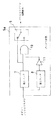
本発明の実施の形態を図1ないし図5に基づいて以下に説明する。本実施の形態に係るインクジェットヘッド制御装置は、ファクシミリ装置等の通信装置やパーソナルコンピュータ等の情報処理装置に内蔵または接続されたインクジェット記録装置に搭載されている。インクジェット記録装置は、図3に示すように、プリンタ・コントローラ17とプリントバッファ18とヘッド駆動部19とCRモータ駆動部20とを有している。ヘッド駆動部19およびCRモータ駆動部20は、インクジェットヘッドである印字ヘッド21およびCRモータ22にそれぞれ接続されている。印字ヘッド21には、インクを噴出させるノズルが例えば64チャンネル分備えられており、各ノズルには、分極処理された圧電材料からなる側壁を有したインク流路が連通されている。そして、このインク流路の側壁面には、側壁内に電界を生成する電極が形成されており、電極には、側壁を変形させる印字パルス電圧および変形後の振動を消失させるストップパルス電圧が印加されるように後述のヘッド駆動部19が接続されている。
【0012】
上記の印字ヘッド21は、図4に示すように、用紙25に対してインクの噴出方向が所定の角度となるようにキャリッジ23に固設されている。キャリッジ23には、主走査方向に横設されたガイド軸24が移動自在に貫挿されていると共に、CRモータ22により駆動される走査ベルト26が接続されており、走査ベルト26を駆動するCRモータ22は、ガイド軸24に沿ってキャリッジ23を主走査方向に進退移動させることによって、印字ヘッド21と用紙25との距離を一定に維持しながら印字ヘッド21を主走査するようになっている。
【0013】
また、キャリッジ23の下面には、光学式や磁気式等の非接触式センサからなるエンコーダ素子27が設けられている。このエンコーダ素子27の検出方向には、多数のスリット部28a…を等間隔に有したタイミングスリット28がガイド軸24に対して平行に設けられており、エンコーダ素子27は、キャリッジ23と共に主走査方向に移動したときに、タイミングスリット28のスリット部28aを検出してエンコーダ信号として出力するようになっている。
【0014】
上記のエンコーダ信号は、図3に示すように、プリンタ・コントローラ17に入力されるようになっている。プリンタ・コントローラ17は、印字タイミング発生部34とバッファ制御部35とCPU部38とI/F制御部42とを有している。そして、印字タイミング発生部34とバッファ制御部35とI/F制御部42とは、ASIC(アプリケーション・スペシフィック・インテグレーテッド・サーキット)等のハードロジック回路により一体的に形成されたASIC部を構成している。
【0015】
上記のASIC部を構成する印字タイミング発生部34は、上述のエンコーダ信号を基にして印字タイミング信号(印字クロック)を形成し、この印字タイミング信号をバッファ制御部35および印字制御部43に出力するようになっている。バッファ制御部35は、図示しないDMAコントローラやアドレスジェネレータ等を有しており、I/F部16を介して入力された印字データをプリントバッファ18に格納する書き込み処理およびプリントバッファ18に格納された印字データを所定のタイミングで読み出して印字制御部43に出力する読み出し処理を実行するようになっている。
【0016】
上記のプリントバッファ18に格納された印字データは、図1に示すように、印字制御部43に出力されるようになっている。印字制御部43は、印字データの入出力を管理すると共にヘッド駆動部19の電圧印加タイミングを設定するヘッド制御部1と、バッファ制御部35からの印字データやストップパルスデータをヘッド駆動部19に出力するデータ加工部2とを有している。データ加工部2は、データセレクタ4と4ビットシフトレジスタ部3とストップパルス生成部5とパラレルシリアル変換部6とをバッファ制御部35側からこの順に接続して有している。4ビットシフトレジスタ部3は、4ビットのシフトレジスタ3aを印字ヘッド21のチャンネル数に対応して64チャンネル分有している。そして、4ビットシフトレジスタ部3およびバッファ制御部35間に配置されたデータセレクタ4は、バッファ制御部35を介して入力されたプリントバッファ18からの各チャンネルの印字データを4ビットシフトレジスタ部3の各シフトレジスタ3aに4ビット単位で分配するようになっている。
【0017】
上記の4ビットシフトレジスタ部3は、印字データを基にしてストップパルスデータを生成するストップパルス生成部5に接続されている。ストップパルス生成部5は、64チャンネル分のデータ判定部5aを有しており、各データ判定部5aには、上述の4ビットシフトレジスタ部3の各シフトレジスタ3aがそれぞれ接続され、各シフトレジスタ3aから印字データが1ビット単位で入力されるようになっている。
【0018】
上記のデータ判定部5aは、図2に示すように、次回(n番目)の印字データとして使用される印字データを格納する第1ラッチ回路7と、第1ラッチ回路7に格納された印字データの次(n+1番目)の印字データを格納する第2ラッチ回路8とを並列接続して有している。第1ラッチ回路7は、2入力のアンド回路10の一方の入力端子に接続されており、第2ラッチ回路8は、ノット回路11を介してアンド回路10の他方の入力端子に接続されている。そして、アンド回路10は、第1ラッチ回路7からの“1”の印字データと第2ラッチ回路8からの“0”の印字データとが入力されたときにのみ、“1”のストップパルスデータを出力するようになっている。尚、印字データの“1”がインク滴の噴射を示し、“0”がインク滴の噴射禁止を示すものとし、ストップパルスデータの“1”がストップパルス電圧の印加を示し、“0”がストップパルス電圧の印加禁止を示すものとする。
【0019】
上記のアンド回路10は、2入力の切換回路9の一方の入力端子に接続されている。また、切換回路9の他方の切換端子には、上述の第1ラッチ回路7が接続されている。そして、アンド回路10からのストップパルスデータと、第1ラッチ回路7からの印字データとがそれぞれ入力される切換回路9は、印字タイミング信号(印字クロック)の略1/2周期で両データを切り換えながらパラレルシリアル変換部6に出力するようになっている。また、パラレルシリアル変換部6は、図1に示すように、全チャンネルの印字データやストップパルスデータが入力されたときに、これらのデータを転送クロックの入力タイミングでヘッド駆動部19にシリアル転送するようになっている。
【0020】
上記のようにして印字データやストップパルスデータがシリアル転送されるヘッド駆動部19は、転送クロックの入力タイミングで各データを順に取り込んでパラレル変換するシリアルパラレル変換回路12を有している。シリアルパラレル変換回路12は、フリップフロップ(F/F)回路13に接続されており、フリップフロップ回路13は、ヘッドストローブ信号に基づいてシリアルパラレル変換回路12のデータ内容を保持および更新するようになっている。そして、フリップフロップ回路13は、AND回路14を介してトランジスタ等を備えたドライバ回路15に接続されており、AND回路14は、Hレベルのファイア信号が入力される毎にフリップフロップ回路13のデータ内容をドライバ回路15に出力し、ドライバ回路15から印字ヘッド21の各チャンネルに印字パルス電圧やストップパルス電圧を出力するようになっている。尚、ファイア信号は、印字タイミング信号と同一周期でHレベルとなる印字パルスと、印字パルスの出力間にHレベルとなるストップパルスとで構成されおり、ストップパルスは、印字後の圧電部材からなる側壁の振動を消失させるのに最適なパルス幅および振動の逆相となる出力タイミングに設定されている。
【0021】
上記の構成において、インクジェットヘッド制御装置の動作について説明する。
【0022】
先ず、ファクシミリ装置等の通信装置が印字データを受信したり、パーソナルコンピュータ等の情報処理装置が印字データを出力することによって、これらの通信装置や情報処理装置に内蔵または接続されたインクジェット記録装置に印字データが入力されると、これらの印字データは、図3に示すように、I/F部16等を介してバッファ制御部35に入力された後、CPU部38から書き込みを行うように指示されたバッファ制御部35によりプリントバッファ18に格納される。
【0023】
プリントバッファ18への印字データの格納が1バンド(64チャンネル)分行われると、次に、バッファ制御部35は、キャリッジ23の移動開始に伴ってCPU部38により読み出し処理を指示され、図1に示すように、プリントバッファ18に格納されている印字データを4ビット単位で読み出して印字制御部43に出力する。そして、印字制御部43に入力された印字データは、4ビットシフトレジスタ部3の各シフトレジスタ3aにデータセレクタ4により分配されながら格納される。
【0024】
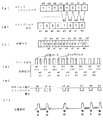
全シフトレジスタ3aに印字データが格納されると、各シフトレジスタ3aの印字データが1ビット単位でストップパルス生成部5の各データ判定部5aに出力される。ここで、特定のチャンネル(例えば0チャンネル)に着目して以降の動作を説明すると、図5(a)に示すように、シフトレジスタ3aに4ビット単位で印字データ(b0“1”,b1“1”,b2“0”,b3“1”)・(b4“0”,b5“1”,b6“1”,b7“1”)が順に格納されるとした場合、シフトレジスタ3aから1ビット単位で印字データb0“1”,b1“1”,b2“0”,b3“1”,・・・がストップパルス生成部5のデータ判定部5aに出力される。
【0025】
これらの印字データb0“1”,b1“1”,b2“0”,b3“1”,・・・が順にデータ判定部5aに入力されると、例えば第1番目の印字データb0“1”が第1ラッチ回路7に保持されながら出力された後、第2番目の印字データb1“1”が第1ラッチ回路7に次の出力データとして格納されると共に第2ラッチ回路8に保持されながら出力される。この後、第3番目の印字データb2“0”がデータ判定部5aに入力されると、第1ラッチ回路7は、第3番目の印字データb2“0”を格納すると共に、格納していた第2番目の印字データb1“1”を出力する。また、第2ラッチ回路8は、第3番目の印字データb2“0”を保持しながら出力する。
【0026】
このようにしてn番目の例えば印字データb0“1”が第1ラッチ回路7から出力されると、この印字データb0“1”は、アンド回路10および切換回路9の一方の入力端子に入力される。また、印字データb0“1”が第1ラッチ回路7から出力されると、n+1番目の印字データb1“1”が第2ラッチ回路8から出力され、この印字データb1“1”は、ノット回路11を介してアンド回路10の他方の入力端子に入力される。これにより、図5(b)に示すように、印字データb0“1”とノット回路11で反転された印字データb1“0”とがアンド回路10に入力されることによって、これらのデータb0“1”・b1“0”を論理積したストップパルスデータa0“0”が切換回路9の他方の入力端子に出力される。この後、図5(c)に示すように、切換回路9において第1ラッチ回路7からの印字データb0“1”と、アンド回路10からのストップパルスデータa0“0”とが切り替えられながらパラレルシリアル変換部6に出力される。
【0027】
上記のようなデータ判定部5aにおける一連の動作は、印字データb0“1”,b1“1”,b2“0”,b3“1”,・・・が入力される毎に順次行われる。そして、これらの印字データb0“1”…やストップパルスデータa0“0”…がパラレルシリアル変換部6に入力されると、図1に示すように、全チャンネルのデータがヘッド制御部1からの転送クロックに同期しながらヘッド駆動部19のシリアルパラレル変換回路12にシリアル転送される。
【0028】
シリアルパラレル変換回路12に入力された全チャンネルのデータは、フリップフロップ回路13にパラレル出力される。そして、フリップフロップ回路13に入力された全チャンネルのデータは、ファイア信号の印字パルスおよびストップパルスに同期するようにヘッドストローブ信号を基にして取り込まれた後、保持されながらAND回路14の一方の入力端子に出力される。この際、AND回路14の他方の入力端子には、ヘッド制御部1からのファイア信号が入力されており、ファイア信号は、印字タイミング信号と同一周期のHレベルの印字パルスとHレベルのストップパルスとを交互に有している。従って、図5(d)に示すように、印字データb0“1”,b1“1”,b2“0”,b3“1”,・・・がAND回路14に入力されたときに、これらのデータとファイア信号の印字パルスとを論理積した出力信号がドライバ回路15に出力される一方、ストップパルスデータa0“0”,a1“1”,a2“0”,a3“1”,・・・がAND回路14に入力されたときに、これらのデータとファイア信号のストップパルスとを論理積した出力信号がドライバ回路15に出力される。
【0029】
これにより、図5(e)に示すように、印字データb0やストップパルスデータa1のようにデータ内容が“1”である場合に、ドライバ回路15が駆動されることによって、印字パルス電圧やストップパルス電圧が印字ヘッド21の所定チャンネルに出力される。そして、図5(f)に示すように、印字パルス電圧が印字ヘッド21に入力されると、所定チャンネルにおけるインク流路の側壁(圧電部材)が印字パルス電圧の印加により変形することによって、インク滴が噴射されて印字が行われる。一方、ストップパルス電圧が印字ヘッド21に入力されると、側壁(圧電部材)の変形により生じた振動の逆相となるタイミングでストップパルス電圧が印加されることによって、側壁の振動が消失する。従って、次回の印字パルス電圧の印加により側壁を変形させる際の振動の影響が除去されることになる。
【0030】
以上のように、本実施形態のインクジェットヘッド制御装置は、図1に示すように、印字データを基にして圧電部材(側壁)に印字パルス電圧を印加し、該圧電部材の変形によりインク流路の容積を増減させることによって、該インク流路に連通したノズルからインク滴を噴射させるものであり、噴射のための印字パルス電圧を圧電部材に印加して変形させた後、該変形により生じた振動を消失させるストップパルス電圧を該圧電部材に印加可能な印字制御部43(ストップパルス制御手段)を有した構成にされている。尚、ストップパルス電圧は、印字パルス電圧により圧電部材が変形されるたびに印加されるようになっていても良いし、変形後の振動が印字品質に悪影響を及ぼすと考えられるときにのみ印加されるようになっていても良い。
【0031】
これにより、印字パルス電圧により圧電部材を変形させた後に、変形による振動が圧電部材に残留していると、この振動が次回の変形時に変形量を減少させる等の悪影響を及ぼす場合があるが、上記の構成によれば、悪影響を及ぼす場合に、圧電部材の振動をストップパルス電圧により消失させて圧電部材を常に一定の変形量で変形させることができる。従って、圧電部材が正規の速度や量で変形せずにインク滴の噴出量が不安定になったときに発生するインク滴の飛散(しぶきの発生)等の不具合を防止することができるため、印字品質を向上させることができる。
【0032】
また、本実施形態において、印字制御部43(ストップパルス制御手段)は、印字データがインク滴の噴射を示す“1”と、噴射禁止を示す“0”とを交互に指示しているか否かを判定するデータ判定部5a(判定手段)を有し、そのデータ判定部5aにより“1”、“0”が交互に指示されていると判定された場合に、ストップパルス電圧を圧電部材に印加させるように構成されている。尚、本実施形態においては、2段のラッチ回路7・8を並列接続することによって、印字データが“1”に続いて“0”を指示するときに、印字データが“1”と“0”とを交互に指示するものと判定しているが、3段のラッチ回路を並列接続することによって、印字データが“1”と“0”と“1”とを連続して指示するときにのみ、ストップパルス電圧を出力するように構成されていても良い。
【0033】
これにより、圧電部材の変形による振動が次回の圧電部材の変形時に最も高い確率で悪影響を及ぼすインク滴の噴射と噴射禁止とを交互に行った場合において、圧電部材の振動をストップパルス電圧により消失させることができることから、圧電部材を常に一定の変形量で変形させて印字品質を向上させることができる。
【0034】
また、本実施形態において、印字制御部43(ストップパルス制御手段)は、圧電部材の変形により生じた振動の逆相となるタイミングでストップパルス電圧を印加させるファイア信号を出力するヘッド制御部1(印加タイミング設定手段)を有した構成にされている。これにより、振動の逆相となるタイミングでストップパルス電圧を印加することによって、振動を確実に消失させることができる。
【0035】
【発明の効果】
請求項1の発明は、印字データを基にして圧電部材に印字パルス電圧を印加し、該圧電部材の変形によりインク流路の容積を増減させることによって、該インク流路に連通したノズルからインク滴を噴射させるインクジェットヘッド制御装置であって、所定の印字データとその次に印字する印字データとが入力されて、前者の印字データがインク滴の噴射を示し、後者の印字データがインク滴の非噴射を示すときには、前者の印字データの後に、その印字パルス電圧により生じた振動を消失させるためのストップパルスデータを付加して出力し、前者及び後者の印字データがともにインク滴の噴射を示すときには、前記ストップパルスデータを出力することなく前者及び後者の印字データを出力する印字制御手段と、そのデータ判定部が出力した前記印字データ及びストップパルスデータが入力され、その印字データ及びストップパルスデータにもとづいて印字パルス電圧及びストップパルス電圧を前記圧電部材に出力するヘッド駆動部とを有している構成である。
【0036】
これにより、印字パルス電圧により圧電部材を変形させた後に、変形による振動が圧電部材に残留していると、この振動が次回の圧電部材の変形時に、変形量を減少させる等の悪影響を及ぼす場合があるが、上記の構成によれば、圧電部材の振動を消失させることができるため、圧電部材を常に一定の変形量で変形させることができ、印字品質を向上させることができるという効果を奏する。
【図面の簡単な説明】
【図1】 インクジェットヘッド制御装置のブロック図である。
【図2】 データ判定部の回路図である。
【図3】 インクジェット記録装置のブロック図である。
【図4】 インクジェット記録装置の要部斜視図である。
【図5】 インクジェットヘッド制御装置の動作状態を示す説明図である。
【符号の説明】
1 ヘッド制御部
2 データ加工部
3 4ビットシフトレジスタ部
3a シフトレジスタ
4 データセレクタ
5 ストップパルス生成部
5a データ判定部
6 パラレルシリアル変換部
7 第1ラッチ回路
8 第2ラッチ回路
9 切換回路
10 アンド回路
11 ノット回路
12 シリアルパラレル変換回路
13 フリップフロップ回路
14 AND回路
15 ドライバ回路
16 I/F部
17 プリンタ・コントローラ
18 プリントバッファ
19 ヘッド駆動部
21 印字ヘッド
22 CRモータ
23 キャリッジ
25 用紙[0001]
BACKGROUND OF THE INVENTION
The present invention relates to an inkjet head control device of an inkjet recording apparatus that prints by ejecting ink.
[0002]
[Prior art]
A communication device such as a facsimile device and an information processing device such as a personal computer usually have a recording device capable of recording these data on paper so as to record data consisting of characters and figures as visual information. In this recording device, various printing methods such as impact method, thermal method, ink jet method, etc. are adopted, but in recent years, ink jet method that is excellent in quietness and can print on paper of various materials is adopted. The ink jet recording apparatus which attracts attention has attracted attention.
[0003]
The above-described inkjet recording apparatus includes an inkjet head having a plurality of channels for ejecting ink droplets on a sheet so as to print characters and figures on the sheet, and an inkjet that drives and controls the inkjet head based on print data. A head control device. Ink jet heads are usually formed by forming a flow path wall of an ink flow path communicating with nozzles from a polarized piezoelectric material and forming electrodes on the wall surface. Conventionally, when the print data instructs ink ejection, the inkjet head control device applies a pulsed print pulse voltage to the corresponding channel electrode to generate an electric field on the flow path wall, By changing the volume of the ink flow path by deforming the path wall, ink droplets are ejected from the nozzles by increasing or decreasing the ink pressure.
[0004]
[Problems to be solved by the invention]
However, in the configuration in which the flow path wall is deformed at an arbitrary time interval based on the print data and ink droplets are ejected as in the conventional case, the piezoelectric member forming the flow path wall vibrates due to the reaction after deformation. Therefore, depending on the next injection timing, vibration due to the previous injection may remain, and the phase of vibration and the start of deformation may be discontinuous. If the phase of vibration and the start of deformation become discontinuous, the flow path wall (piezoelectric member) cannot be deformed at a normal speed or amount, and the ejection amount of ink droplets becomes unstable. This results in a decrease in print quality such as ink droplets splashing on the paper (splashing).
[0005]
Therefore, the present invention intends to provide an ink jet head control device capable of eliminating vibration after deformation of a piezoelectric member forming a flow path wall so that good print quality can always be obtained. .
[0006]
[Means for Solving the Problems]
In order to solve the above-mentioned problems, the invention of
[0007]
As a result, after the piezoelectric member is deformed by the printing pulse voltage, if vibration due to the deformation remains in the piezoelectric member, this vibration may adversely affect the amount of deformation at the next deformation of the piezoelectric member. However, according to the above configuration, since the vibration of the piezoelectric member can be eliminated, the piezoelectric member can always be deformed with a constant deformation amount, and the printing quality can be improved.
[0008]
A second aspect of the present invention is the ink jet head control apparatus according to the first aspect, wherein the print control means determines the predetermined print data and a latch circuit that holds the next print data, and each print data. And determining means.
[0009]
Thereby, the print control means determines each print data held in the latch circuit and outputs stop pulse data.
[0010]
Invention 請 Motomeko 3, an inkjet head control apparatus according to
[0011]
DETAILED DESCRIPTION OF THE INVENTION
An embodiment of the present invention will be described below with reference to FIGS. The ink jet head control apparatus according to the present embodiment is mounted on an ink jet recording apparatus built in or connected to a communication apparatus such as a facsimile apparatus or an information processing apparatus such as a personal computer. As shown in FIG. 3, the ink jet recording apparatus includes a
[0012]
As shown in FIG. 4, the
[0013]
An
[0014]
The encoder signal is input to the
[0015]
The print
[0016]
The print data stored in the
[0017]
The 4-bit
[0018]
As shown in FIG. 2, the
[0019]
The AND
[0020]
The
[0021]
The operation of the inkjet head control device in the above configuration will be described.
[0022]
First, when a communication device such as a facsimile device receives print data or an information processing device such as a personal computer outputs print data, an ink jet recording device built in or connected to the communication device or information processing device is used. When the print data is input, as shown in FIG. 3, the print data is input to the
[0023]
When storage of print data in the
[0024]
When the print data is stored in all the shift registers 3a, the print data of each shift register 3a is output to each
[0025]
When these print data b0 “1”, b1 “1”, b2 “0”, b3 “1”,... Are sequentially input to the
[0026]
When the n-th print data b0 “1” is output from the first latch circuit 7 in this way, the print data b0 “1” is input to one input terminal of the AND
[0027]
A series of operations in the
[0028]
The data of all channels input to the serial / parallel conversion circuit 12 are output in parallel to the flip-flop circuit 13. The data of all the channels input to the flip-flop circuit 13 is taken in based on the head strobe signal so as to synchronize with the print pulse and stop pulse of the fire signal, and then held in one of the AND
[0029]
As a result, as shown in FIG. 5E, when the data content is “1” such as the print data b0 and the stop pulse data a1, the
[0030]
As described above, the ink jet head control apparatus according to the present embodiment applies a print pulse voltage to a piezoelectric member (side wall) based on print data as shown in FIG. Ink droplets are ejected from the nozzles communicating with the ink flow path by increasing or decreasing the volume of the ink. The print pulse voltage for ejection is applied to the piezoelectric member to cause deformation, and then the deformation is caused by the deformation. A print control unit 43 (stop pulse control means) is provided that can apply a stop pulse voltage that eliminates vibration to the piezoelectric member. The stop pulse voltage may be applied every time the piezoelectric member is deformed by the printing pulse voltage, or is applied only when the vibration after deformation is considered to adversely affect printing quality. You may come to be.
[0031]
Thereby, after the piezoelectric member is deformed by the printing pulse voltage, if vibration due to the deformation remains in the piezoelectric member, this vibration may adversely affect the amount of deformation at the next deformation, According to the above configuration, in the case of adverse effects, the vibration of the piezoelectric member can be eliminated by the stop pulse voltage, and the piezoelectric member can always be deformed with a constant deformation amount. Therefore, since the piezoelectric member is not deformed at a normal speed and amount, problems such as ink droplet scattering (occurrence of splashing) that occurs when the ejection amount of the ink droplet becomes unstable can be prevented. Printing quality can be improved.
[0032]
In the present embodiment, the print control unit 43 (stop pulse control means) determines whether or not the print data alternately indicates “1” indicating ejection of ink droplets and “0” indicating ejection prohibition. A
[0033]
As a result, the vibration of the piezoelectric member disappears due to the stop pulse voltage when the ink droplet ejection and the ejection prohibition, which are most adversely affected by the deformation of the piezoelectric member at the next deformation, are alternately performed. Therefore, it is possible to improve the printing quality by always deforming the piezoelectric member with a constant deformation amount.
[0034]
In the present embodiment, the print control unit 43 (stop pulse control means) outputs a fire signal that applies a stop pulse voltage at a timing that is in reverse phase of the vibration caused by the deformation of the piezoelectric member. (Application timing setting means). As a result, the vibration can be reliably eliminated by applying the stop pulse voltage at a timing that is in the opposite phase of the vibration.
[0035]
【The invention's effect】
According to the first aspect of the present invention, a printing pulse voltage is applied to the piezoelectric member based on the printing data, and the volume of the ink flow path is increased or decreased by deformation of the piezoelectric member, so that the ink from the nozzle communicating with the ink flow path An inkjet head control device that ejects droplets, wherein predetermined print data and print data to be printed next are input, the former print data indicates ejection of ink droplets, and the latter print data indicates ink droplets when showing the non-injection, after the former print data, and the stop pulse data by adding the output for dissipating the vibration generated by the printing pulse voltage, the former and the latter printing data are both drop ejection when the indicating includes print control means for outputting the former and latter print data without outputting the stop pulse data, the data determination unit is output It said print data and the stop pulse data is input, is configured to have a head driving unit that outputs a printing pulse voltages and a stop pulse voltage on the basis of the print data and the stop pulse data to said piezoelectric member.
[0036]
As a result, after the piezoelectric member is deformed by the printing pulse voltage, if vibration due to the deformation remains in the piezoelectric member, this vibration may adversely affect the amount of deformation at the next deformation of the piezoelectric member. However, according to the above configuration, since the vibration of the piezoelectric member can be eliminated, the piezoelectric member can be always deformed with a constant deformation amount, and the print quality can be improved. .
[Brief description of the drawings]
FIG. 1 is a block diagram of an inkjet head control device.
FIG. 2 is a circuit diagram of a data determination unit.
FIG. 3 is a block diagram of an ink jet recording apparatus.
FIG. 4 is a perspective view of a main part of the ink jet recording apparatus.
FIG. 5 is an explanatory diagram illustrating an operation state of the inkjet head control device.
[Explanation of symbols]
DESCRIPTION OF
Claims (3)
所定の印字データとその次に印字する印字データとが入力されて、前者の印字データがインク滴の噴射を示し、後者の印字データがインク滴の非噴射を示すときには、前者の印字データの後に、その印字パルス電圧により生じた振動を消失させるためのストップパルスデータを付加して出力し、前者及び後者の印字データがともにインク滴の噴射を示すときには、前記ストップパルスデータを出力することなく前者及び後者の印字データを出力する印字制御手段と、
そのデータ判定部が出力した前記印字データ及びストップパルスデータが入力され、その印字データ及びストップパルスデータにもとづいて印字パルス電圧及びストップパルス電圧を前記圧電部材に出力するヘッド駆動部と、
を有していることを特徴とするインクジェットヘッド制御装置。Ink jet head control for ejecting ink droplets from nozzles communicating with the ink flow path by applying a print pulse voltage to the piezoelectric member based on the print data and increasing or decreasing the volume of the ink flow path by deformation of the piezoelectric member A device,
Print data and is input to be printed and the next predetermined print data, the former printing data indicates the ejection of ink droplets, when the latter print data indicates a non-ejection of ink droplets, the former printing data After that, stop pulse data for eliminating the vibration caused by the print pulse voltage is added and output. When both the former and latter print data indicate ejection of ink droplets, the stop pulse data is output. Print control means for outputting the former and the latter print data ,
The print data and stop pulse data output by the data determination unit are input, and a head drive unit that outputs a print pulse voltage and a stop pulse voltage to the piezoelectric member based on the print data and stop pulse data;
An inkjet head control device comprising:
前記所定の印字データとその次の印字データを保持するラッチ回路と、各印字データを判定する判定手段とを有することを特徴とする請求項1記載のインクジェットヘッド制御装置。The print control means includes
2. The ink jet head control apparatus according to claim 1, further comprising: a latch circuit that holds the predetermined print data and the next print data; and a determination unit that determines each print data.
前記振動の逆相となるタイミングで前記ストップパルス電圧を出力することを特徴とする請求項1または2に記載のインクジェットヘッド制御装置。The head drive unit is
The ink jet head control device according to claim 1 or 2, characterized in that outputs the stop pulse voltage at the timing when the opposite phase of the vibration.
Priority Applications (1)
| Application Number | Priority Date | Filing Date | Title |
|---|---|---|---|
| JP10147397A JP3713882B2 (en) | 1997-04-18 | 1997-04-18 | Inkjet head control device |
Applications Claiming Priority (1)
| Application Number | Priority Date | Filing Date | Title |
|---|---|---|---|
| JP10147397A JP3713882B2 (en) | 1997-04-18 | 1997-04-18 | Inkjet head control device |
Related Child Applications (1)
| Application Number | Title | Priority Date | Filing Date |
|---|---|---|---|
| JP2003426754A Division JP3711995B2 (en) | 2003-12-24 | 2003-12-24 | Inkjet recording device |
Publications (2)
| Publication Number | Publication Date |
|---|---|
| JPH10291308A JPH10291308A (en) | 1998-11-04 |
| JP3713882B2 true JP3713882B2 (en) | 2005-11-09 |
Family
ID=14301711
Family Applications (1)
| Application Number | Title | Priority Date | Filing Date |
|---|---|---|---|
| JP10147397A Expired - Fee Related JP3713882B2 (en) | 1997-04-18 | 1997-04-18 | Inkjet head control device |
Country Status (1)
| Country | Link |
|---|---|
| JP (1) | JP3713882B2 (en) |
Families Citing this family (1)
| Publication number | Priority date | Publication date | Assignee | Title |
|---|---|---|---|---|
| US7399042B2 (en) | 2004-03-31 | 2008-07-15 | Seiko Epson Corporation | Head driving device |
-
1997
- 1997-04-18 JP JP10147397A patent/JP3713882B2/en not_active Expired - Fee Related
Also Published As
| Publication number | Publication date |
|---|---|
| JPH10291308A (en) | 1998-11-04 |
Similar Documents
| Publication | Publication Date | Title |
|---|---|---|
| US5357268A (en) | Ink jet recording head in which the ejection elements are driven in blocks | |
| US7753464B2 (en) | Liquid-jet apparatus | |
| JP4929637B2 (en) | Head drive apparatus and head drive method for ink jet printer | |
| JP4196523B2 (en) | Recording device | |
| JP2000158643A5 (en) | ||
| JP3556794B2 (en) | Inkjet printer | |
| JP4729935B2 (en) | Ink jet printer, head drive device for ink jet printer, head drive method for ink jet printer | |
| JP4529120B2 (en) | Liquid ejector | |
| JP3713882B2 (en) | Inkjet head control device | |
| JP2003103777A (en) | Liquid jetting apparatus | |
| JP2002019107A (en) | Recorder | |
| JP3711995B2 (en) | Inkjet recording device | |
| JP3656443B2 (en) | Ink droplet ejection device | |
| JP4710643B2 (en) | Inkjet printer head driving method and inkjet printer | |
| JP4701967B2 (en) | Head drive apparatus and head drive method for ink jet printer | |
| JP4956901B2 (en) | Liquid ejector | |
| JP2933970B2 (en) | Recording method and recording apparatus using the recording method | |
| JP4725307B2 (en) | Inkjet printer | |
| JP5115620B2 (en) | Inkjet printer head drive apparatus and inkjet printer head drive method | |
| JP2007118290A (en) | Driving device for inkjet printer, and its driving method | |
| JP2007001027A (en) | Device for driving head of inkjet printer and driving method | |
| JP4899592B2 (en) | Ink jet printer and ink jet printer driving method | |
| JP3658216B2 (en) | Recording head and recording apparatus using the recording head | |
| JP2007001261A (en) | Liquid injection apparatus | |
| JP3320531B2 (en) | Ink jet device |
Legal Events
| Date | Code | Title | Description |
|---|---|---|---|
| A521 | Written amendment |
Free format text: JAPANESE INTERMEDIATE CODE: A523 Effective date: 20040414 |
|
| A621 | Written request for application examination |
Free format text: JAPANESE INTERMEDIATE CODE: A621 Effective date: 20040414 |
|
| A977 | Report on retrieval |
Free format text: JAPANESE INTERMEDIATE CODE: A971007 Effective date: 20041217 |
|
| A131 | Notification of reasons for refusal |
Free format text: JAPANESE INTERMEDIATE CODE: A131 Effective date: 20041228 |
|
| A521 | Written amendment |
Free format text: JAPANESE INTERMEDIATE CODE: A523 Effective date: 20050222 |
|
| TRDD | Decision of grant or rejection written | ||
| A01 | Written decision to grant a patent or to grant a registration (utility model) |
Free format text: JAPANESE INTERMEDIATE CODE: A01 Effective date: 20050802 |
|
| A61 | First payment of annual fees (during grant procedure) |
Free format text: JAPANESE INTERMEDIATE CODE: A61 Effective date: 20050815 |
|
| R150 | Certificate of patent or registration of utility model |
Free format text: JAPANESE INTERMEDIATE CODE: R150 |
|
| FPAY | Renewal fee payment (event date is renewal date of database) |
Free format text: PAYMENT UNTIL: 20090902 Year of fee payment: 4 |
|
| FPAY | Renewal fee payment (event date is renewal date of database) |
Free format text: PAYMENT UNTIL: 20090902 Year of fee payment: 4 |
|
| FPAY | Renewal fee payment (event date is renewal date of database) |
Free format text: PAYMENT UNTIL: 20100902 Year of fee payment: 5 |
|
| FPAY | Renewal fee payment (event date is renewal date of database) |
Free format text: PAYMENT UNTIL: 20110902 Year of fee payment: 6 |
|
| FPAY | Renewal fee payment (event date is renewal date of database) |
Free format text: PAYMENT UNTIL: 20110902 Year of fee payment: 6 |
|
| FPAY | Renewal fee payment (event date is renewal date of database) |
Free format text: PAYMENT UNTIL: 20120902 Year of fee payment: 7 |
|
| FPAY | Renewal fee payment (event date is renewal date of database) |
Free format text: PAYMENT UNTIL: 20130902 Year of fee payment: 8 |
|
| LAPS | Cancellation because of no payment of annual fees |