JP3713332B2 - Single crystal copper target and manufacturing method thereof - Google Patents
Single crystal copper target and manufacturing method thereof Download PDFInfo
- Publication number
- JP3713332B2 JP3713332B2 JP18136196A JP18136196A JP3713332B2 JP 3713332 B2 JP3713332 B2 JP 3713332B2 JP 18136196 A JP18136196 A JP 18136196A JP 18136196 A JP18136196 A JP 18136196A JP 3713332 B2 JP3713332 B2 JP 3713332B2
- Authority
- JP
- Japan
- Prior art keywords
- copper
- target
- single crystal
- wiring
- purity
- Prior art date
- Legal status (The legal status is an assumption and is not a legal conclusion. Google has not performed a legal analysis and makes no representation as to the accuracy of the status listed.)
- Expired - Lifetime
Links
Images

Landscapes
- Manufacture And Refinement Of Metals (AREA)
- Physical Vapour Deposition (AREA)
- Crystals, And After-Treatments Of Crystals (AREA)
Description
【0001】
【発明の属する技術分野】
本発明は、信頼性を高めた半導体素子配線膜形成用ターゲットおよび超LSIの内部配線に使用される銅配線に関するものである。従来より、超LSI配線材料としては、電気抵抗が低く、Siとの密着性の高いΑl合金が一般的に用いられていた。しかしながら、LSIの高集積化による配線の微細化にともない、エレクトロマイグレーション(EM),ストレスマイグレーション(SM)などに起因した断線による素子の信頼性低下が問題となるに至っている。
【0002】
この問題を解決するために、Al合金に代わる配線材料の開発が検討されその内の1種として銅材が使用されるようになった。銅は電気抵抗がAlの2/3と低い為、Αlに比較して電流密度を大きくでき、また融点もΑlに比較して400℃以上高いことから、超LSI用内部配線として使用した場合、エレクトロマイグレーシヨン(EM)、ストレスマイグレーシヨン(SM)にも強い配線材料として有力視されている。
【0003】
【従来の技術】
その結果、無酸素銅あるいは、電解銅より作られたスパッタリング・ターゲットを用いて、銅配線が形成されるようになったが、これらの銅材は純度が99.99%程度である為、得られる薄膜の純度も同程度の粗悪なものであった。この様な低純度の配線材料を用いて行なわれた試験においては、銅のメリットである耐EM性や耐SM性は失われ、耐腐食性の低さが問題となり、問題を解決する方策として次の様な方法が提案されている。
【0004】
たとえば、特開平5−311424号公報に記載されている様に、純度6N(99.9999%)以上の高純度銅を原料として、Ti(チタン)、Zn(亜鉛)を微量元素として添加する方法が考案された。しかしながら、この方法は原料鋳塊の製造工程が複雑になるため、ターゲットの製品コストを上昇させる結果となった。また、特開平3−166731号公報に記載されている様に、熱処理により、銅配線の結晶粒を粗大化させて酸化の進行経路となる結晶粒界を減少させ、耐酸化性を向上させる方法が考案されたが、この方法は、成膜後熱処埋を行なう為、LSIのプロセスコストが上昇するという問題があった。
【0005】
また、配線幅の減少にともない、成膜中の異常放電による配線欠陥や、ピンホールと呼ばれる穴の発生も深刻な問題となった。この原因について、鋭意研究をおこなった結果、従来のターゲットを製造する工程に、ターゲットの品質を低下させる原因があったことが判明した。以下に、従来の銅ターゲットの製造工程を説明する。
▲1▼原料となる銅の鋳塊を鍛造および圧延により所定の寸法まで機械加工する。この時、鋳塊に強加工を施すことにより鋳造組織を破壊し、配向性の無い、lmm以下の微細な集合組織の圧延板とする。
▲2▼圧延板は、必要に応じて熱処理を施し、表面研削、外形加工、洗浄を行なった後、ターゲットとなる。この様にして加工されたターゲットにおいては、加工により組織が、1mm以下の微細な結晶の集合となっている為、結晶粒界には、加工中に発生した、酸化物、硫化物、あるいは、不純物が凝集して存在している。こうした純度の低い粗悪なターゲットを用いて成膜を行なうと、膜中に混入した酸化物や硫化物が腐食の原因となる。また、結晶粒界に電界が集中し、異常放電を起し、粒界部より粒状の銅(以下、パーティクルと呼ぶ)が放出され、成膜面に付着する。こうした付着物は薄膜配線のピンホールとなり、配線間を短絡させる原因となる。こうした理由から、従来技術においては、銅のメリットである耐EM性や耐SM性等の優れた特徴を充分に生かす事ができなかった。
【0006】
【発明が解決しようとする課題】
上述のように超LSI配線に使用される銅配線材料には、極めて高い純度が要求される。特に、不純物として、ナトリウムやカリウムなどのアルカリ金属が配線中に存在すると、酸化膜耐圧劣化の原因となり素子の信頼性を著しく低下させることとなる。こうした観点から、電解精製やゾーン精製法を用いて製造された高純度銅を原料とするスパッタリングターゲットが製造され、成膜材料として検討されてきた。しかし、加工工程における汚染を完全に排除することができないばかりでなく、加工組織である結晶粒界に酸化物、硫化物、不純物が濃縮蓄積される問題が残されていた。
【0007】
こうした不純物は、LSIのパッケージの外部より侵入してくる水分等との反応により腐食の原因となる。成膜中に放出される微量な酸素は、膜を酸化させ抵抗率を上昇させるとともに、酸化による腐食発生の起源となる。また、粒界を起点として、発生する異常放電により、パーティクルが発生し配線間を短絡させる原因となっていた。本発明は、上記事情に鑑みてなされたもので、スパッタリング法によって、高純度銅をターゲットとして配線を形成する場合、耐EM性、耐SM性、耐酸化性および耐腐食性に優れた、銅薄膜配線を提供するものである。
【0008】
【課題を解決するための手段】
本発明者らはかかる課題を解決するために鋭意研究したところ、純度99.9999wt%以上の高純度銅を基体金属として、酸素濃度が0.1ppm以下の雰囲気にて溶解凝固させて得た高純度銅単結晶体を用いることによって、これらの課題が解決できることを見出し本発明を達成することができた。すなわち本発明の第1は純度99.9999wt%以上の単結晶銅からなるスパッタリングターゲットであり;第2は上記単結晶銅は、酸素が0.05ppm以下、水素が0.2ppm以下、窒素が0.5ppm以下、炭素が0.01ppm以下で、純度が99.9999wt%以上であることを特徴とする上記第1記載のスパッタリングターゲットであり;第3は純度99.9999wt%以上の単結晶銅を(111)方向に切断した後、研磨加工を行ってターゲット材とすることを特徴とするスパッタリングターゲットの製造方法である。
【0009】
【発明実施の形態】
本発明で半導体素子の配線用スパッタリングターゲットとして使用する高純度銅単結晶体は、出発原料として銀と硫黄の合計含有量が0.5ppm 以下である純度99.9999wt%以上の高純度銅を用い、真空炉内の原料るつぼに入れた後、真空度1×10⁻³Torr以下、炉内温度1085℃以上で加熱溶解(第1工程)したものを、上記原料るつぼ底部と溶解滴下孔を介して接続する単結晶鋳型に流し込んだ後、順次、該単結晶鋳型を冷却することによってO2 ガス成分およびN2 ガス成分が合計で1ppm 以下である内径4インチの高純度銅単結晶体である。
【0010】
この単結晶体を(111)方向に切断した後鏡面研磨を行ってターゲットとするが、この単結晶体の溶存ガス成分について分析したところ、酸素(O)は、<0.03ppm 、硫黄(S)は<0.01ppm 、水素(H)は<0.2ppm 、窒素は0.5ppm 以下であった。次いで上記組成からなるターゲットを用い、RFスパッター法によりArガス圧力、1×10⁻²Torr以下、好ましくは3×10⁻³Torr、放電電力を200〜800Wで放電試験を行い、Si基板上にバリア膜としてTiN膜を被覆させた後、0.5〜1.0μm厚の銅配線を形成した後、保護膜としてSiN膜を堆積させて半導体素子とした。
【0011】
このように本発明の銅薄膜形成用単結晶スパッタリングターゲットは、スパッタリング法により銅配線として使用される銅薄膜を形成するが、従来法に比較して耐食性が高く、耐EM性、耐SM性に優れており、今後の半導体素子等の配線の微細化を担う有望な材料となっている。以下、実施例を以て詳細に説明するが、本発明の範囲はこれらに限定されるものではない。
【0012】
【実施例1】
図1に示す製造装置を用いて高純度銅単結晶体を得た。先ず出発原料として銀と硫黄の合計含有量が0.1ppm 以下である純度99.9999wt%以上の高純度銅10kgを原料るつぼ5内に入れ、炉内真空度を4×10⁻⁴Torrとし、温度1150℃一定でるつぼ内の原料を溶解した。溶解された銅は、るつぼ底部に設けられた溶解滴下孔4から下方の単結晶鋳型6に滴下するが下部ヒーター12を1000℃までは0.5℃/分の割合で、1000℃からは15℃/分の割合で温度を下げて、4インチ口径の単結晶体10kgを得た。次いで得られた単結晶体を、X線カット面検査装置で(111)方向に切断した後鏡面研磨を行い直径6インチ、厚さ5mmのターゲットを作製した。このターゲットの不純物分析をグロー放電質量分析法により行ったところ、不純物金属成分は原料の分析値と同一であるが、ガス不純物の分析値は表に示す通りであった。
【0013】
【表1】

【0014】
次に、このターゲットを用いて、RFスパッター法により、Arガス圧力3×10⁻³Torr、放電電力それぞれ250W、500Wとし放電試験を行なった。この場合、成膜中の放電状態は、マルチチャンネルホトディテクターにより観察し、放出ガス、異常放電の発性を記録した。その結果を表2に示した。
【0015】
【表2】
【0016】
【表3】
【0017】
次に、この(111)方位の6N−銅単結晶ターゲットを用いて、RFスパッター法により、幅0.3μm、厚さ0.8μmの銅配線を形成した。この時の成膜条件は、Arガス圧力3×10⁻³Torr、放電電力250Wとし、Si基板上に堆積させた。得られた薄膜について、2結晶X線回折装置により結晶性を評価したところ、(111)に配向し、半値幅は、100秒とほぼ単結晶に近い薄膜であった。
【0018】
次いで、保護膜として、CVD法により、厚さ0.8μmのSiN膜を堆積させて所望の半導体素子とした。この場合、加速試験に先立ち、成膜中に生じたピンホール等に起因する初期断線率を調べたところ、0.09%であった。次いで、初期断線を除外した試料について電流密度1×10⁶ A/cm2 、雰囲気温度200℃にて、2000時間の加速試験を行ない断線不良率を測定した。その結果、断線不良率は、1.0%と低かった。
【0019】
【実施例2】
出発原料として7N高純度銅を用いたほかは、実施例1と同一の条件で4インチ口径の7N高純度銅単結晶体を得、X線カット面検査装置を用いて(111)方向に切断した後、鏡面研磨を行い直径6インチ、厚さ5mmのターゲットを作製した。このターゲットの不純物分折をグロー放電質量分折法により行ったところ、不純物金属成分は、原料の分折値と同一であるが、ガス不純物の分折値は、表4に示す通りであった。
【0020】
【表4】
【0021】
次いで、このターゲットを用いて、RFスパッター法によりArガス圧力3×10⁻³Torr、放電電力250W、500Wとして放電試験を行ない、異常放電回数およびパーティクルの発生状況を調べた。その結果、実施例1に記載した表2および表3と同様の結果となった。また、プラズマ分光の結果、ターゲットよりの放出ガスと思われるものは検出されなかった。
【0022】
次に、この(111)方位の7N−単結晶銅ターゲットを用いて、RFスパッター法により、幅0.3μm、厚さ0.8μmの銅配線を形成した。この時の成膜条件は、Arガス圧力3×10⁻³Torr、放電電力500Wとし、Si基板上に堆積させた。得られた薄膜について、2結晶X線回折装置により結晶性を評価したところ、(111)に配向し、半値幅は、85秒とほぼ単結晶に近い薄膜であった。
【0023】
次いで、保護膜として、CVD法により、厚さ0.8μmのSiN膜を堆積させ所望の半導体素子とした。この場合、加速試験に先立ち、成膜中に生じたピンホール等に起因した初期断線率を調べたところ、0.09%であった。
次いで、初期断線を除外した試料について電流密度1×10⁶ A/cm2 、雰囲気温度200℃にて、2000時間の加速試験を行ない断線不良率を測定したところ断線不良率は0.5%と低かった。
【0024】
【比較例】
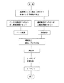
実施例1で得た6N高純度銅単結晶体を原料として、図2に示すフローシートに従って鍛造により厚さ3cmまで加工を施して、単結晶鋳塊の組織を微細な多結晶とした。次いで、硝酸によりエッチングを行なった後、加工歪を除去する目的で、高純度アルゴン雰囲気にて約135℃、30分の焼鈍を行なった。焼鈍後の結晶粒径は、1mm以下であった。次に、クロス圧延により、板厚7mmとした。圧延板は、表面研削および外形加工により、直径6インチ、厚さ5mmの円盤となしこれを有機洗浄後、希硝酸によるエッチングを行なって、ターゲットとした。
【0025】
ターゲットの不純物分折を、グロー放電質量分折法によりおこなったところ、不純物金属成分は、原料の分折値と同一であるが、ガス不純物については表1に示すように実施例1および実施例2に比較して相当高かった。
【0026】
このターゲットについて、X線回折パターンを測定したところ、複数の回折線が得られたことから、特定な方位への配向は確認されなかった。次いで、このターゲットを用いて、RFスパッター法により、Arガス圧力3×10⁻³Torr、放電電力250W、500Wとし放電試験を行なった。異常放電回数およびパーティクルの発生状況は、実施例1および実施例2に準じて行ない、その結果を表5および表6に示したが、実施例1に比較して異常放電回数やパーティクル発生枚数が多いことが明白である。
【0027】
【表5】
【表6】
【0029】
次にこの6N−高純度銅多結晶ターゲットを用いて、RFスパッター法により、幅0.3μm、厚さ0.8μmの銅配線を形成した。この時の成膜条件は、Arガス圧力3×10⁻³Torr、放電電力500Wとし、Si基板上にバリア膜としてTiN膜を被覆させた後、堆積させたが、この時の銅配線の結晶粒径は0.06μmから0.lμm程度と微細なものであった。X線回折パターンも、多結晶特有の複数の回折線を示し、配向は認められなかった。
【0030】
次に、保護膜としてCVD法により、厚さ0.8μmのSiN膜を堆積させた。加速試験に先立ち、成膜中に生じたピンホール等に起因した初期断線率を調べたところ、0.8%であった。次に、初期断線を除外した試料について電流密度1×10⁶ A/cm2 、雰囲気温度200℃にて、2000時間の加速試験を行い断線不良率を測定したところ、断線不良率は2.5%と実施例1に比較しても多かった。
【0031】
【発明の効果】
本発明は上述のように新規な高純度銅単結晶体を加工して得られたスパッタリングターゲート並びに該タゲーットを用いて成膜した配線を有する半導体素子であり従来品に比較して初期断線率や断線不良率の低い超LSI向け銅配線を得ることができるものである。
【図面の簡単な説明】
【図1】本発明ターゲット材料の製造装置の概略構造を示す模式図である。
【図2】比較例および従来のターゲットの製造工程を示すフローシートである。
【符号の説明】
1 電気炉
2 真空排気装置
3 石英外筒
4 溶解滴下孔
5 原料るつぼ
6 単結晶鋳型
7 水冷フランジ
8 断熱トラップ
9 冷却水
10 上部ヒーター
11 中部ヒーター
12 下部ヒーター[0001]
BACKGROUND OF THE INVENTION
The present invention relates to a semiconductor device wiring film forming target with improved reliability and a copper wiring used for an internal wiring of a VLSI. Conventionally, as a VLSI wiring material, a metal alloy having low electrical resistance and high adhesion to Si has been generally used. However, along with the miniaturization of wiring due to high integration of LSIs, the reliability of elements due to disconnection due to electromigration (EM), stress migration (SM), etc. has become a problem.
[0002]
In order to solve this problem, development of a wiring material to replace the Al alloy has been studied, and a copper material has been used as one of them. Since copper has a low electrical resistance of 2/3 that of Al, the current density can be increased compared to Αl, and the melting point is higher than 400 ℃ compared to Αl, so when used as internal wiring for VLSI, It is regarded as a promising wiring material for electro migration (EM) and stress migration (SM).
[0003]
[Prior art]
As a result, copper wiring has been formed using a sputtering target made of oxygen-free copper or electrolytic copper, but since these copper materials have a purity of about 99.99%, they can be obtained. The purity of the resulting thin film was also inferior. In tests conducted using such low-purity wiring materials, EM resistance and SM resistance, which are the merits of copper, are lost, and low corrosion resistance becomes a problem. The following methods have been proposed.
[0004]
For example, as described in JP-A-5-31424, a method of adding high purity copper having a purity of 6N (99.9999%) or more as a raw material and adding Ti (titanium) and Zn (zinc) as trace elements Was devised. However, this method complicates the manufacturing process of the raw material ingot, resulting in an increase in the target product cost. Further, as described in JP-A-3-166673, a method for improving the oxidation resistance by coarsening the crystal grains of the copper wiring and reducing the crystal grain boundaries that become the progress path of oxidation by heat treatment. However, this method has a problem that the process cost of the LSI increases because the thermal treatment is performed after the film formation.
[0005]
As the wiring width is reduced, wiring defects due to abnormal discharge during film formation and the generation of holes called pinholes have become serious problems. As a result of diligent research on this cause, it has been found that the process of manufacturing a conventional target had a cause of reducing the quality of the target. Below, the manufacturing process of the conventional copper target is demonstrated.
(1) A copper ingot as a raw material is machined to a predetermined size by forging and rolling. At this time, the cast structure is destroyed by subjecting the ingot to strong processing to obtain a rolled sheet having a fine texture of 1 mm or less and having no orientation.
{Circle around (2)} The rolled plate is subjected to heat treatment as necessary, and after being subjected to surface grinding, outer shape processing and cleaning, it becomes a target. In the target processed in this way, the structure is a collection of fine crystals of 1 mm or less by processing, so the crystal grain boundary has oxide, sulfide, or Impurities are present in aggregate. When film formation is performed using such a poor target with low purity, oxides and sulfides mixed in the film cause corrosion. In addition, the electric field concentrates on the crystal grain boundary, causing abnormal discharge, and granular copper (hereinafter referred to as particles) is released from the grain boundary part and adheres to the film formation surface. Such deposits become pinholes in the thin film wiring and cause a short circuit between the wirings. For these reasons, in the prior art, it was not possible to make full use of excellent features such as EM resistance and SM resistance, which are merits of copper.
[0006]
[Problems to be solved by the invention]
As described above, the copper wiring material used for the VLSI wiring is required to have extremely high purity. In particular, when an alkali metal such as sodium or potassium is present in the wiring as an impurity, the breakdown voltage of the oxide film is deteriorated and the reliability of the device is remarkably lowered. From such a viewpoint, a sputtering target using high-purity copper produced by electrolytic purification or zone purification as a raw material has been manufactured and studied as a film forming material. However, not only the contamination in the processing process cannot be completely eliminated, but also a problem that oxides, sulfides, and impurities are concentrated and accumulated at the grain boundaries as the processing structure.
[0007]
Such impurities cause corrosion due to reaction with moisture or the like entering from the outside of the LSI package. The trace amount of oxygen released during film formation oxidizes the film to increase the resistivity, and causes the occurrence of corrosion due to oxidation. In addition, due to abnormal discharge that occurs from the grain boundary as a starting point, particles are generated, causing a short circuit between the wirings. The present invention has been made in view of the above circumstances. When a wiring is formed by sputtering using high-purity copper as a target, the copper is excellent in EM resistance, SM resistance, oxidation resistance, and corrosion resistance. A thin film wiring is provided.
[0008]
[Means for Solving the Problems]
The inventors of the present invention have intensively studied to solve such problems. As a result, a high purity copper obtained by dissolving and solidifying in an atmosphere having an oxygen concentration of 0.1 ppm or less using high purity copper having a purity of 99.9999 wt% or more as a base metal. It has been found that these problems can be solved by using a pure copper single crystal, and the present invention has been achieved. That is, the first of the present invention is a sputtering target made of single crystal copper having a purity of 99.9999 wt% or more; the second is that the single crystal copper has oxygen of 0.05 ppm or less, hydrogen of 0.2 ppm or less, and nitrogen of 0. .5 ppm or less, carbon is 0.01 ppm or less, and the purity is 99.9999 wt% or more. The third is the sputtering target according to the first aspect; the third is a single crystal copper having a purity of 99.9999 wt% or more. A method of manufacturing a sputtering target, comprising cutting the substrate in a (111) direction and performing a polishing process to obtain a target material.
[0009]
DETAILED DESCRIPTION OF THE INVENTION
The high-purity copper single crystal used as a sputtering target for wiring of a semiconductor element in the present invention uses high-purity copper having a purity of 99.9999 wt% or more with a total content of silver and sulfur being 0.5 ppm or less as a starting material. After being put in the raw material crucible in the vacuum furnace, heated and melted (first step) at a vacuum degree of 1 × 10 −3 Torr or lower and a furnace temperature of 1085 ° C. or higher through the bottom of the raw material crucible and the melting dropping hole. After flowing into the single crystal template to be connected, the single crystal template is sequentially cooled to obtain a high-purity copper single crystal having an inner diameter of 4 inches in which O 2 gas component and N 2 gas component are 1 ppm or less in total. .
[0010]
This single crystal is cut in the (111) direction and then mirror-polished to obtain a target. When the dissolved gas component of this single crystal is analyzed, oxygen (O) is <0.03 ppm, sulfur (S ) Was <0.01 ppm, hydrogen (H) was <0.2 ppm, and nitrogen was 0.5 ppm or less. Next, using a target having the above composition, an RF sputtering method is used to perform a discharge test at an Ar gas pressure of 1 × 10 −2 Torr or less, preferably 3 × 10 −3 Torr, and a discharge power of 200 to 800 W. After coating a TiN film as a barrier film, a copper wiring having a thickness of 0.5 to 1.0 μm was formed, and then a SiN film was deposited as a protective film to obtain a semiconductor element.
[0011]
As described above, the single crystal sputtering target for forming a copper thin film of the present invention forms a copper thin film used as a copper wiring by a sputtering method, but has higher corrosion resistance, EM resistance, and SM resistance than the conventional method. It is excellent and has become a promising material for miniaturization of wiring of future semiconductor elements and the like. Hereinafter, although an Example demonstrates in detail, the scope of the present invention is not limited to these.
[0012]
[Example 1]
A high-purity copper single crystal was obtained using the manufacturing apparatus shown in FIG. First, 10 kg of high-purity copper having a purity of 99.9999 wt% or more having a total content of silver and sulfur of 0.1 ppm or less as a starting material is placed in the
[0013]
[Table 1]
[0014]
Next, using this target, a discharge test was performed by an RF sputtering method at an Ar gas pressure of 3 × 10 −3 Torr and a discharge power of 250 W and 500 W, respectively. In this case, the discharge state during film formation was observed with a multi-channel photo detector, and the emitted gas and the occurrence of abnormal discharge were recorded. The results are shown in Table 2.
[0015]
[Table 2]
[0016]
[Table 3]
[0017]
Next, a copper wiring having a width of 0.3 μm and a thickness of 0.8 μm was formed by RF sputtering using this (111) -oriented 6N-copper single crystal target. The film formation conditions at this time were an Ar gas pressure of 3 × 10 −3 Torr and a discharge power of 250 W, which were deposited on the Si substrate. When the crystallinity of the obtained thin film was evaluated by a two-crystal X-ray diffractometer, the film was oriented to (111) and the half-value width was 100 seconds, which was almost a single crystal.
[0018]
Next, as a protective film, a SiN film having a thickness of 0.8 μm was deposited by a CVD method to obtain a desired semiconductor element. In this case, when the initial disconnection rate due to pinholes or the like generated during the film formation was examined prior to the acceleration test, it was 0.09%. Next, an accelerated test for 2000 hours was performed at a current density of 1 × 10 6 A / cm 2 and an ambient temperature of 200 ° C. for the sample excluding the initial disconnection, and the disconnection failure rate was measured. As a result, the disconnection failure rate was as low as 1.0%.
[0019]
[Example 2]
A 7N high purity copper single crystal having a 4 inch diameter was obtained under the same conditions as in Example 1 except that 7N high purity copper was used as a starting material, and was cut in the (111) direction using an X-ray cut surface inspection device. Then, mirror polishing was performed to prepare a target having a diameter of 6 inches and a thickness of 5 mm. When the impurity analysis of this target was performed by the glow discharge mass spectrometry, the impurity metal component was the same as the analysis value of the raw material, but the analysis value of the gas impurity was as shown in Table 4. .
[0020]
[Table 4]
[0021]
Next, using this target, a discharge test was conducted by RF sputtering with Ar gas pressure of 3 × 10 −3 Torr, discharge power of 250 W, and 500 W, and the number of abnormal discharges and the state of generation of particles were examined. As a result, the same results as in Table 2 and Table 3 described in Example 1 were obtained. As a result of plasma spectroscopy, no gas that seems to be emitted from the target was detected.
[0022]
Next, a copper wiring having a width of 0.3 μm and a thickness of 0.8 μm was formed by RF sputtering using the (111) -oriented 7N-single-crystal copper target. The film formation conditions at this time were an Ar gas pressure of 3 × 10 −3 Torr and a discharge power of 500 W, which were deposited on the Si substrate. When the crystallinity of the obtained thin film was evaluated by a two-crystal X-ray diffractometer, it was oriented to (111) and the half-value width was 85 seconds, which was a thin film almost similar to a single crystal.
[0023]
Then, a SiN film having a thickness of 0.8 μm was deposited as a protective film by a CVD method to obtain a desired semiconductor element. In this case, when the initial disconnection rate due to pinholes and the like generated during the film formation was examined prior to the acceleration test, it was 0.09%.
Next, the sample with the initial disconnection excluded was subjected to an accelerated test for 2000 hours at a current density of 1 × 10 6 A / cm 2 and an atmospheric temperature of 200 ° C., and the disconnection failure rate was measured to be 0.5%. It was low.
[0024]
[Comparative example]
The 6N high-purity copper single crystal obtained in Example 1 was used as a raw material and processed to a thickness of 3 cm by forging according to the flow sheet shown in FIG. 2 to make the structure of the single crystal ingot a fine polycrystal. Next, after etching with nitric acid, annealing was performed at about 135 ° C. for 30 minutes in a high purity argon atmosphere for the purpose of removing processing strain. The crystal grain size after annealing was 1 mm or less. Next, the plate thickness was set to 7 mm by cross rolling. The rolled plate was formed into a disk having a diameter of 6 inches and a thickness of 5 mm by surface grinding and outer shape processing, and this was subjected to organic cleaning, followed by etching with dilute nitric acid to obtain a target.
[0025]
When impurity analysis of the target was performed by glow discharge mass spectrometry, the impurity metal component was the same as the analysis value of the raw material, but for gas impurities, as shown in Table 1, Example 1 and Example It was considerably higher than 2.
[0026]
When an X-ray diffraction pattern was measured for this target, a plurality of diffraction lines were obtained, and no orientation in a specific direction was confirmed. Next, using this target, a discharge test was performed by an RF sputtering method with an Ar gas pressure of 3 × 10 −3 Torr, a discharge power of 250 W, and 500 W. The number of abnormal discharges and the occurrence state of particles were performed in accordance with Example 1 and Example 2, and the results are shown in Tables 5 and 6. Compared to Example 1, the number of abnormal discharges and the number of particles generated are different. It is clear that there are many.
[0027]
[Table 5]
[Table 6]
[0029]
Next, a copper wiring having a width of 0.3 μm and a thickness of 0.8 μm was formed by RF sputtering using this 6N-high purity copper polycrystalline target. The film formation conditions at this time were an Ar gas pressure of 3 × 10 −3 Torr and a discharge power of 500 W, and a TiN film was deposited as a barrier film on the Si substrate, and then deposited. The particle size is 0.06 μm to 0. It was as fine as about 1 μm. The X-ray diffraction pattern also showed a plurality of diffraction lines peculiar to polycrystals, and no orientation was observed.
[0030]
Next, a SiN film having a thickness of 0.8 μm was deposited as a protective film by a CVD method. Prior to the acceleration test, the initial disconnection rate due to pinholes and the like generated during film formation was examined and found to be 0.8%. Next, a sample with the initial disconnection excluded was subjected to an accelerated test for 2000 hours at a current density of 1 × 10 6 A / cm 2 and an ambient temperature of 200 ° C., and the disconnection failure rate was measured. % And even in comparison with Example 1.
[0031]
【The invention's effect】
The present invention is a semiconductor element having a sputtering gate obtained by processing a novel high-purity copper single crystal as described above, and a wiring formed using the taggate, and has an initial disconnection rate as compared with a conventional product. In addition, a copper wiring for a VLSI with a low disconnection failure rate can be obtained.
[Brief description of the drawings]
FIG. 1 is a schematic view showing a schematic structure of an apparatus for producing a target material of the present invention.
FIG. 2 is a flow sheet showing a manufacturing process of a comparative example and a conventional target.
[Explanation of symbols]
DESCRIPTION OF SYMBOLS 1
Claims (3)
Priority Applications (1)
| Application Number | Priority Date | Filing Date | Title |
|---|---|---|---|
| JP18136196A JP3713332B2 (en) | 1996-06-21 | 1996-06-21 | Single crystal copper target and manufacturing method thereof |
Applications Claiming Priority (1)
| Application Number | Priority Date | Filing Date | Title |
|---|---|---|---|
| JP18136196A JP3713332B2 (en) | 1996-06-21 | 1996-06-21 | Single crystal copper target and manufacturing method thereof |
Related Child Applications (1)
| Application Number | Title | Priority Date | Filing Date |
|---|---|---|---|
| JP2005212483A Division JP4206403B2 (en) | 2005-07-22 | 2005-07-22 | Manufacturing method of semiconductor internal wiring |
Publications (2)
| Publication Number | Publication Date |
|---|---|
| JPH108244A JPH108244A (en) | 1998-01-13 |
| JP3713332B2 true JP3713332B2 (en) | 2005-11-09 |
Family
ID=16099388
Family Applications (1)
| Application Number | Title | Priority Date | Filing Date |
|---|---|---|---|
| JP18136196A Expired - Lifetime JP3713332B2 (en) | 1996-06-21 | 1996-06-21 | Single crystal copper target and manufacturing method thereof |
Country Status (1)
| Country | Link |
|---|---|
| JP (1) | JP3713332B2 (en) |
Families Citing this family (26)
| Publication number | Priority date | Publication date | Assignee | Title |
|---|---|---|---|---|
| JP3725621B2 (en) * | 1996-06-21 | 2005-12-14 | 同和鉱業株式会社 | High-purity silver wire for recording or sound or image transmission |
| US6627149B1 (en) | 1996-06-21 | 2003-09-30 | Dowa Mining Co., Ltd. | High-purity silver wires for use in recording, acoustic or image transmission applications |
| JP3727115B2 (en) * | 1996-08-16 | 2005-12-14 | 同和鉱業株式会社 | Manufacturing method of sputtering target |
| JP3403918B2 (en) * | 1997-06-02 | 2003-05-06 | 株式会社ジャパンエナジー | High purity copper sputtering target and thin film |
| US6569270B2 (en) | 1997-07-11 | 2003-05-27 | Honeywell International Inc. | Process for producing a metal article |
| JP4058777B2 (en) * | 1997-07-31 | 2008-03-12 | 日鉱金属株式会社 | High purity ruthenium sintered compact sputtering target for thin film formation and thin film formed by sputtering the target |
| JP3872233B2 (en) * | 1999-06-29 | 2007-01-24 | 京セラ株式会社 | Silicon casting method |
| US6878250B1 (en) | 1999-12-16 | 2005-04-12 | Honeywell International Inc. | Sputtering targets formed from cast materials |
| US6331233B1 (en) | 2000-02-02 | 2001-12-18 | Honeywell International Inc. | Tantalum sputtering target with fine grains and uniform texture and method of manufacture |
| US7517417B2 (en) | 2000-02-02 | 2009-04-14 | Honeywell International Inc. | Tantalum PVD component producing methods |
| JP2001240949A (en) * | 2000-02-29 | 2001-09-04 | Mitsubishi Materials Corp | Method of manufacturing for worked billet of high- purity copper having fine crystal grain |
| WO2001094660A2 (en) * | 2000-06-02 | 2001-12-13 | Honeywell International Inc. | Sputtering target |
| JP2002129313A (en) * | 2000-10-20 | 2002-05-09 | Nikko Materials Co Ltd | High purity copper sputtering target generating reduced particles |
| JP4421335B2 (en) * | 2004-03-05 | 2010-02-24 | 株式会社東芝 | Method for producing sputtering target and method for producing copper wiring film |
| JP4505731B2 (en) * | 2004-07-27 | 2010-07-21 | 三菱マテリアル株式会社 | Method for producing high purity copper ingot with low carbon content |
| JP4421586B2 (en) * | 2006-09-21 | 2010-02-24 | 株式会社東芝 | Method for producing sputtering target and method for producing copper wiring film |
| WO2010038641A1 (en) | 2008-09-30 | 2010-04-08 | 日鉱金属株式会社 | High-purity copper and process for electrolytically producing high-purity copper |
| WO2010038642A1 (en) * | 2008-09-30 | 2010-04-08 | 日鉱金属株式会社 | High-purity copper or high-purity copper alloy sputtering target, process for manufacturing the sputtering target, and high-purity copper or high-purity copper alloy sputtered film |
| JP5638697B2 (en) * | 2012-01-25 | 2014-12-10 | Jx日鉱日石金属株式会社 | High purity copper chrome alloy sputtering target |
| KR20140138111A (en) * | 2012-03-09 | 2014-12-03 | 후루카와 덴키 고교 가부시키가이샤 | Sputtering target |
| JP6182296B2 (en) * | 2012-03-09 | 2017-08-16 | 古河電気工業株式会社 | Sputtering target and manufacturing method thereof |
| DE112015006364T5 (en) * | 2015-03-23 | 2017-11-30 | Pusan National University Industrial-University Cooperation Foundation | A method of producing a copper thin film by using a single crystal copper target |
| JP6066007B1 (en) | 2016-05-10 | 2017-01-25 | 日立金属株式会社 | Method for producing purified copper and method for producing electric wire |
| JP6066010B1 (en) * | 2016-06-28 | 2017-01-25 | 日立金属株式会社 | Method for producing purified copper and electric wire |
| CN112845838A (en) * | 2020-11-25 | 2021-05-28 | 长沙理工大学 | High-temperature forming device for imperfect monocrystalline germanium wafer |
| CN112795876B (en) * | 2020-12-31 | 2023-08-08 | 松山湖材料实验室 | Copper target and preparation method thereof |
-
1996
- 1996-06-21 JP JP18136196A patent/JP3713332B2/en not_active Expired - Lifetime
Also Published As
| Publication number | Publication date |
|---|---|
| JPH108244A (en) | 1998-01-13 |
Similar Documents
| Publication | Publication Date | Title |
|---|---|---|
| JP3713332B2 (en) | Single crystal copper target and manufacturing method thereof | |
| KR100338796B1 (en) | High-purity copper sputtering targets and thin films | |
| JP3727115B2 (en) | Manufacturing method of sputtering target | |
| EP0915177B1 (en) | Highly purified hafnium and sputtering target using the same | |
| JP4223511B2 (en) | Copper alloy sputtering target, method of manufacturing the same, and semiconductor element wiring | |
| JPH1180942A (en) | Ta sputtering target, its production and assembled body | |
| JP3413782B2 (en) | Titanium target for sputtering and method for producing the same | |
| JP2009149996A (en) | Sputter target | |
| JP2015061943A (en) | High-purity copper manganese alloy sputtering target | |
| Moon et al. | Observed correlation of Sn oxide film to Sn whisker growth in Sn-Cu electrodeposit for Pb-free solders | |
| JP2005330591A (en) | Sputtering target | |
| JP3974945B2 (en) | Titanium sputtering target | |
| JP2000034562A (en) | Sputtering target and part used in apparatus for forming thin film | |
| JP3819487B2 (en) | Manufacturing method of semiconductor device | |
| TWI525207B (en) | Cu alloy thin film forming sputtering target and its manufacturing method | |
| JP4206403B2 (en) | Manufacturing method of semiconductor internal wiring | |
| JP2921799B2 (en) | Method for manufacturing high-purity sputter target for semiconductor element formation | |
| JP2015203148A (en) | Copper alloy material, ceramic wiring board and production method of ceramic wiring board | |
| Chin et al. | Effect of the tantalum barrier layer on the electromigration and stress migration resistance of physical-vapor-deposited copper interconnect | |
| TW202246534A (en) | Ag alloy film, and Ag alloy sputtering target | |
| WO2013133353A1 (en) | Sputtering target | |
| JP3228660B2 (en) | Method for producing high-purity metal material for semiconductor element formation | |
| TW201504462A (en) | High-purity copper-cobalt alloy sputtering target | |
| JP4555797B2 (en) | Semiconductor element | |
| JPH0813141A (en) | Sputtering target and its production |
Legal Events
| Date | Code | Title | Description |
|---|---|---|---|
| RD02 | Notification of acceptance of power of attorney |
Free format text: JAPANESE INTERMEDIATE CODE: A7422 Effective date: 20040206 |
|
| RD04 | Notification of resignation of power of attorney |
Free format text: JAPANESE INTERMEDIATE CODE: A7424 Effective date: 20040318 |
|
| A977 | Report on retrieval |
Free format text: JAPANESE INTERMEDIATE CODE: A971007 Effective date: 20050516 |
|
| A131 | Notification of reasons for refusal |
Free format text: JAPANESE INTERMEDIATE CODE: A131 Effective date: 20050524 |
|
| A521 | Written amendment |
Free format text: JAPANESE INTERMEDIATE CODE: A523 Effective date: 20050722 |
|
| TRDD | Decision of grant or rejection written | ||
| A01 | Written decision to grant a patent or to grant a registration (utility model) |
Free format text: JAPANESE INTERMEDIATE CODE: A01 Effective date: 20050816 |
|
| A61 | First payment of annual fees (during grant procedure) |
Free format text: JAPANESE INTERMEDIATE CODE: A61 Effective date: 20050822 |
|
| R150 | Certificate of patent or registration of utility model |
Free format text: JAPANESE INTERMEDIATE CODE: R150 |
|
| FPAY | Renewal fee payment (event date is renewal date of database) |
Free format text: PAYMENT UNTIL: 20080826 Year of fee payment: 3 |
|
| S111 | Request for change of ownership or part of ownership |
Free format text: JAPANESE INTERMEDIATE CODE: R313111 |
|
| FPAY | Renewal fee payment (event date is renewal date of database) |
Free format text: PAYMENT UNTIL: 20080826 Year of fee payment: 3 |
|
| R350 | Written notification of registration of transfer |
Free format text: JAPANESE INTERMEDIATE CODE: R350 |
|
| FPAY | Renewal fee payment (event date is renewal date of database) |
Free format text: PAYMENT UNTIL: 20080826 Year of fee payment: 3 |
|
| FPAY | Renewal fee payment (event date is renewal date of database) |
Free format text: PAYMENT UNTIL: 20090826 Year of fee payment: 4 |
|
| FPAY | Renewal fee payment (event date is renewal date of database) |
Free format text: PAYMENT UNTIL: 20090826 Year of fee payment: 4 |
|
| FPAY | Renewal fee payment (event date is renewal date of database) |
Free format text: PAYMENT UNTIL: 20100826 Year of fee payment: 5 |
|
| FPAY | Renewal fee payment (event date is renewal date of database) |
Free format text: PAYMENT UNTIL: 20110826 Year of fee payment: 6 |
|
| FPAY | Renewal fee payment (event date is renewal date of database) |
Free format text: PAYMENT UNTIL: 20110826 Year of fee payment: 6 |
|
| FPAY | Renewal fee payment (event date is renewal date of database) |
Free format text: PAYMENT UNTIL: 20120826 Year of fee payment: 7 |
|
| FPAY | Renewal fee payment (event date is renewal date of database) |
Free format text: PAYMENT UNTIL: 20120826 Year of fee payment: 7 |
|
| FPAY | Renewal fee payment (event date is renewal date of database) |
Free format text: PAYMENT UNTIL: 20130826 Year of fee payment: 8 |
|
| R250 | Receipt of annual fees |
Free format text: JAPANESE INTERMEDIATE CODE: R250 |
|
| R250 | Receipt of annual fees |
Free format text: JAPANESE INTERMEDIATE CODE: R250 |
|
| R250 | Receipt of annual fees |
Free format text: JAPANESE INTERMEDIATE CODE: R250 |
|
| EXPY | Cancellation because of completion of term |