JP3713019B2 - Gyroscope and manufacturing method thereof - Google Patents
Gyroscope and manufacturing method thereof Download PDFInfo
- Publication number
- JP3713019B2 JP3713019B2 JP2002564435A JP2002564435A JP3713019B2 JP 3713019 B2 JP3713019 B2 JP 3713019B2 JP 2002564435 A JP2002564435 A JP 2002564435A JP 2002564435 A JP2002564435 A JP 2002564435A JP 3713019 B2 JP3713019 B2 JP 3713019B2
- Authority
- JP
- Japan
- Prior art keywords
- electrode
- displacement
- detection
- gyroscope
- fixed
- Prior art date
- Legal status (The legal status is an assumption and is not a legal conclusion. Google has not performed a legal analysis and makes no representation as to the accuracy of the status listed.)
- Expired - Fee Related
Links
Images


Classifications
-
- G—PHYSICS
- G01—MEASURING; TESTING
- G01C—MEASURING DISTANCES, LEVELS OR BEARINGS; SURVEYING; NAVIGATION; GYROSCOPIC INSTRUMENTS; PHOTOGRAMMETRY OR VIDEOGRAMMETRY
- G01C19/00—Gyroscopes; Turn-sensitive devices using vibrating masses; Turn-sensitive devices without moving masses; Measuring angular rate using gyroscopic effects
- G01C19/02—Rotary gyroscopes
-
- B—PERFORMING OPERATIONS; TRANSPORTING
- B81—MICROSTRUCTURAL TECHNOLOGY
- B81B—MICROSTRUCTURAL DEVICES OR SYSTEMS, e.g. MICROMECHANICAL DEVICES
- B81B3/00—Devices comprising flexible or deformable elements, e.g. comprising elastic tongues or membranes
- B81B3/0064—Constitution or structural means for improving or controlling the physical properties of a device
- B81B3/0067—Mechanical properties
- B81B3/0078—Constitution or structural means for improving mechanical properties not provided for in B81B3/007 - B81B3/0075
-
- B—PERFORMING OPERATIONS; TRANSPORTING
- B81—MICROSTRUCTURAL TECHNOLOGY
- B81B—MICROSTRUCTURAL DEVICES OR SYSTEMS, e.g. MICROMECHANICAL DEVICES
- B81B3/00—Devices comprising flexible or deformable elements, e.g. comprising elastic tongues or membranes
- B81B3/0062—Devices moving in two or more dimensions, i.e. having special features which allow movement in more than one dimension
-
- G—PHYSICS
- G01—MEASURING; TESTING
- G01C—MEASURING DISTANCES, LEVELS OR BEARINGS; SURVEYING; NAVIGATION; GYROSCOPIC INSTRUMENTS; PHOTOGRAMMETRY OR VIDEOGRAMMETRY
- G01C19/00—Gyroscopes; Turn-sensitive devices using vibrating masses; Turn-sensitive devices without moving masses; Measuring angular rate using gyroscopic effects
- G01C19/56—Turn-sensitive devices using vibrating masses, e.g. vibratory angular rate sensors based on Coriolis forces
- G01C19/5719—Turn-sensitive devices using vibrating masses, e.g. vibratory angular rate sensors based on Coriolis forces using planar vibrating masses driven in a translation vibration along an axis
- G01C19/5733—Structural details or topology
- G01C19/5755—Structural details or topology the devices having a single sensing mass
-
- B—PERFORMING OPERATIONS; TRANSPORTING
- B81—MICROSTRUCTURAL TECHNOLOGY
- B81B—MICROSTRUCTURAL DEVICES OR SYSTEMS, e.g. MICROMECHANICAL DEVICES
- B81B2201/00—Specific applications of microelectromechanical systems
- B81B2201/02—Sensors
- B81B2201/0228—Inertial sensors
- B81B2201/0242—Gyroscopes
-
- B—PERFORMING OPERATIONS; TRANSPORTING
- B81—MICROSTRUCTURAL TECHNOLOGY
- B81B—MICROSTRUCTURAL DEVICES OR SYSTEMS, e.g. MICROMECHANICAL DEVICES
- B81B2203/00—Basic microelectromechanical structures
- B81B2203/01—Suspended structures, i.e. structures allowing a movement
- B81B2203/0136—Comb structures
-
- B—PERFORMING OPERATIONS; TRANSPORTING
- B81—MICROSTRUCTURAL TECHNOLOGY
- B81B—MICROSTRUCTURAL DEVICES OR SYSTEMS, e.g. MICROMECHANICAL DEVICES
- B81B2203/00—Basic microelectromechanical structures
- B81B2203/04—Electrodes
Abstract
Description
【0001】
発明の背景
(a)発明の属する技術分野
本発明は微細加工(micromachining)方法を利用して製造したジャイロスコープ及びその製造方法に関する。
【0002】
(b)従来の技術
微細加工を利用した様々な応用分野の中で、慣性センサ(Inertial sensor)への応用は早くから関心を集めた分野である。シリコンを材料として微細加工で製作された慣性センサは安価、大量生産、そして、集積化が可能であるという長所によって最近十年間商品化慣性センサを開発するための研究が活発に進められている。しかし、実際商品化が可能な水準のジャイロスコープが製作されて発表されたのは最近何年間かのことであって、まだ微細加工で製作されたジャイロスコープが商品化された例はない。商品化のためには広い動作範囲と共に、低い出力値を雑音と分離して選択的に検出して、高い感度を獲得することが必要であり、既存の半導体工程と完全に互換できる工程を利用したり、単純な工程を利用して低価格の素子を具現しなければならない。また、素子の信頼性及び高い収率もやはり保障されなければならない。
【0003】
Analog Devices Inc.(ADI)の場合、1998年に1個当り$30のジャイロスコープを目標に表面微細加工工程を利用して真空で動作する集積化ジャイロスコープの試作品を開発したが、当時、圧電素子を利用したジャイロスコープが自動車用の場合、$15、カメラ用の場合、$5の非常に安い値段で市販されていたため、これらと競争するためには新たな接近方法が求められた。そのために、ADIは素子の小型化とパッケージ工程の最少化による低価格のジャイロスコープ開発に努力した。素子の小型化のために、全素子サイズのほとんどを占める回路部分を減らして、それにともなう問題をジャイロスコープの機械部分を大きくすることにより解決し、全体的な素子のサイズは減らす方向を模索するようになった。また、機械部分が大きければ相対的に低いQ値でも動作して、商品化のための二つの目標、つまり小さいサイズの素子と真空パッケージの削除を満足することができると考えられる。実際に真空パッケージをしなければならない素子の場合、一般的なIC工程でのパッケージ工程が占める値段比率が50%であるのに比べて80%という大きな値段比率を占めているので、これを解決することが全素子の値段を低くするのに必要である。
【0004】
発明の要旨
本発明が目的とする技術的課題は、大気圧で動作できるジャイロスコープを提供することにある。
【0005】
本発明の他の技術的課題は、高い周波数で大きな駆動変位を有するジャイロスコープを提供することにある。
【0006】
本発明が解決しようとする他の技術的課題は、駆動モードと検出モード間の機械的干渉が排除されたジャイロスコープを提供することにある。
【0007】
本発明が解決しようとする他の技術的課題は、周波数チューニングがなくても高い感度を示すジャイロスコープを提供することにある。
【0008】
本発明が解決しようとする他の技術的課題は、ジャイロスコープの製造方法を単純化させることである。
【0009】
このような課題を解決するために本発明では、駆動変位電極と検出変位電極を慣性質量体と折りたたみスプリングを媒介として連結することにより駆動変位電極と検出変位電極との間の機械的干渉を排除する。
【0010】
具体的には、本発明の1態様としてのジャイロスコープは、固定されている駆動固定電極、駆動固定電極の対向電極で第1方向への変位が可能な駆動変位電極、駆動変位電極に連結されていて駆動変位電極の第1方向変位に沿って第1方向に変位し、角速度印加時に第2方向に変位する慣性質量体、慣性質量体に連結されていて慣性質量体の第2方向変位に沿って第2方向に変位することができる検出変位電極、及び、検出変位電極の対向電極で固定されている検出固定電極とを有する。
【0011】
この時、駆動変位電極は第1方向に移動できる折りたたみスプリングによって支持されており、検出変位電極は第2方向に移動できる折りたたみスプリングによって支持される。
【0012】
また、駆動変位電極と慣性質量体は第2方向に移動することができて固定軸のない折りたたみスプリングによって連結されており、検出変位電極と慣性質量体は第1方向に移動することができて固定軸のない折りたたみスプリングによって連結される。
【0013】
また、検出変位電極は慣性質量体を中心にして両側に二つが配置されており、ジャイロスコープは二つの検出変位電極を連結するエッジジンバルをさらに含むことができ、慣性質量体の中心には孔が形成されており、孔の中心に位置して固定されている変位制限軸をさらに含むことができる。
【0014】
また、検出変位電極の両側に対称的に形成されていて、電気的スプリングの役割を果たして検出変位電極の共振周波数を変化させて検出感度を調節するチューニング電極をさらに含むことができる。
【0015】
このようなジャイロスコープは、(a)シリコン基板とガラス基板を正極接合する段階、(b)前記シリコン基板をエッチング、研磨して特定の厚さに作る段階、(c)前記シリコン基板上に金属層を形成する段階、(d)前記金属層と前記シリコン基板をフォトリソグラフィ(photolithography)によってジャイロスコープパターンを有するシリコン構造体を形成する段階、(e)前記ガラス基板をエッチングし、前記シリコン構造体のうち複数の固定軸を除いた残りの部分をガラス基板から分離して、前記固定軸によって固定されている駆動固定電極と、前記駆動固定電極の対向電極であって、第1方向への変位が可能な駆動変位電極と、前記駆動変位電極に連結されており、前記駆動変位電極の第1方向変位に沿って第1方向に変位し、角速度印加時に第2方向に変位する慣性質量体と、前記慣性質量体に連結されており、前記慣性質量体の第2方向変位に沿って第2方向に変位することができる検出変位電極と、前記検出変位電極の対向電極で、前記固定軸によって固定されている検出固定電極と、を含み、前記駆動変位電極は第1方向に移動することができる折りたたみスプリングによって支持されており、前記検出変位電極は第2方向に移動できる折りたたみスプリングによって支持され、前記駆動変位電極と前記慣性質量体とは第2方向に移動することができ、前記固定軸のない折りたたみスプリングによって連結されており、前記検出変位電極と前記慣性質量体とは第1方向に移動することができ、前記固定軸のない折りたたみスプリングによって連結されているジャイロスコープ構造体を形成する段階、(f)前記ジャイロスコープ構造体をフリップチップボンディングして外部回路と連結する段階を含む方法を使用して製作する。
【0016】
この時、(d)と(e)との間にシリコン基板とガラス基板をダイシングして個別素子単位に分離する段階をさらに含むことができる。
【0017】
(c)で形成する金属層はCrとAuの二重層であるのが好ましく、(e)でガラス基板はHF溶液を使用してエッチングされる。
【0018】
HF溶液を使用したガラス基板のエッチングの深さは10μm以上にして空気減衰を最少にし、ジャイロスコープを大気圧下で作動可能にする。
【0019】
(b)でシリコン基板のエッチングは80℃の36wt.%のKOH水溶液を使用して行うのが好ましい。
【0020】
図面の簡単な説明
本発明の実施例の詳細部分の構成について完全に理解するために、添付の図面を参照して説明する。
図1は、本発明の実施例によるジャイロスコープの斜視図である。
図2は、本発明の実施例によるジャイロスコープの平面図である。
図3は、図1の一部拡大図である。
図4は、本発明の実施例によって製造されたジャイロスコープの部分SEM写真である。
図5は、本発明の実施例によるジャイロスコープの駆動または検出スプリング部の拡大図である。
図6は、本発明の実施例によって製造されたジャイロスコープの駆動または検出スプリング部のSEM写真である。
図7は、本発明の実施例によるジャイロスコープの駆動または検出連結スプリング部の概念図である。
図8は、変位制限部による共振駆動及び検出変位グラフである。
図9(a)乃至図9(h)は、本発明の実施例によってジャイロスコープを製造する過程を示した図である。
【0021】
好適実施例の詳細説明
以下に、本発明の好ましい実施例について詳細な説明を示し、発明者の実施した最適な発明の実施の方法について示す。上述したように、本発明は、発明から逸脱しない限り多様に変形して実施することが可能であり、記載した説明及び図面に限定されるものではない。
【0022】
図1は本発明の実施例によるジャイロスコープの斜視図であり、図2は本発明の実施例によるジャイロスコープの平面図、図3は図1の一部拡大図であり、図4は本発明の実施例によって製造されたジャイロスコープの部分SEM(Scanning Electron Microscope)写真である。
【0023】
本発明の実施例によるジャイロスコープはガラス基板10とその上に形成されているシリコン構造体とを備える。ガラス基板10上部にはシリコン構造体を支持してシリコン構造体の固定軸を固定する支柱11、12、13が形成されている。
【0024】
シリコン構造体は、駆動部、検出部、多数のスプリング、チューニング(tuning)電極34及び変位制限軸33からなる。駆動部は、駆動固定電極26、駆動変位電極24及び慣性質量体23からなる。検出部は、検出固定電極25、検出変位電極22及びエッジジンバル(gimbal)21からなる。スプリングは、駆動変位電極24を振動させることができるように支持する駆動スプリング28、29、検出変位電極22とエッジジンバル21が振動できるように支持する検出スプリング27、30、駆動変位電極24と慣性質量体23とを連結する駆動連結スプリング31と、検出変位電極22と慣性質量体23とを連結する検出連結スプリング32を備える。また、駆動スプリング28、29は、外部駆動スプリング28と内部駆動スプリング29とに区分され、検出スプリング27、30は夫々、外部検出スプリング27と内部検出スプリング30に区分される。
【0025】
以下、これら各要素の構造及び機能についてより詳細に説明する。
【0026】
まず、駆動部の駆動固定電極26は、ガラス基板10の支柱12によって固定されており、四角形凹凸形態の対向部を有する。駆動変位電極24は外部及び内部駆動スプリング28、29によって支持されていて東西方向(図1と図2のコンパス方向参照)にだけ移動することができ、四角形凹凸形態に形成されている対向部を有する。駆動固定電極26の対向部と駆動変位電極24の対向部とは互いに噛み合う形態に配置されている。外部及び内部駆動スプリング28、29はガラス基板10の支柱13によって固定されており、板スプリングが南北方向に長く配置されていて東西方向にだけ移動することができる。慣性質量体23は駆動連結スプリング31を通じて駆動変位電極24と連結されていて、駆動変位電極24が東西方向に振動すると、慣性質量体23は駆動変位電極24と共に振動するようになっている。この時、駆動連結スプリング31は固定軸がなく南北方向にだけ移動することができるため、駆動変位電極24の東西方向振動を慣性質量体23にそのまま伝達する。
【0027】
次に、検出部の検出固定電極25は、ガラス基板10の支柱12によって固定されており、四角形凹凸形態の対向部を有する。検出変位電極22は外部及び内部検出スプリング27、30によって支持されていて南北方向(図1と図2のコンパス方向参照)にだけ移動することができ、四角形凹凸形態に形成されている対向部を有する。検出固定電極25の対向部と検出変位電極22の対向部とは互いに噛み合う形態に配置されている。外部及び内部検出スプリング27、30はガラス基板10の支柱13によって固定されており、板スプリングが東西方向に長く配置されていて南北方向にだけ移動することができる。検出変位電極22は検出連結スプリング32を通じて慣性質量体23と連結されていて、慣性質量体23が南北方向に振動すると、検出変位電極22は慣性質量体23と共に振動するようになっている。この時、検出連結スプリング32は固定軸がなく東西方向にだけ移動することができるため、慣性質量体23の南北方向振動を検出変位電極22にそのまま伝達する。エッジジンバル21は駆動部と検出部全体を囲んでおり、慣性質量体23を中心にして南北両側に位置する検出変位電極22を一つに連結している。したがって、両検出変位電極22は同一な方向と変位をもって運動する。
【0028】
チューニング電極34は南北両検出変位電極22の東西両側に各々一つずつ4個が形成されており、ガラス基板10の支柱11によって固定されている。チューニング電極34の検出変位電極22と対向する面には四角形凹凸が形成されており、検出変位電極22にもチューニング電極34と対向する面には四角形凹凸が形成されている。検出変位電極22の四角形凹凸とチューニング電極34の四角形凹凸は互いに凸部は凸部同士に、凹部は凹部同士に対向している。
【0029】
変位制限軸33は慣性質量体23の中央部分に形成されている孔の中心に形成されており、慣性質量体が一定の量以上変位することを防止する役割を果たすもので、ガラス基板10の支柱(図示せず)によって固定されている。慣性質量体23が停止している状態では慣性質量体23と一定の間隔をおいて分離されている。
【0030】
このような構造のジャイロスコープの駆動及び検出方法について説明する。
【0031】
駆動固定電極26に電源を印加すると、駆動変位電極24は駆動固定電極26に印加される電源の周波数によって静電気的に駆動されて東西方向に振動する。慣性質量体23も駆動変位電極24と同様に振動する。この状態でジャイロスコープが回転力を受けると、慣性質量体23は南北方向への力を受けて南北方向にも振動するようになる。慣性質量体23の南北方向振動は検出変位電極22にそのまま伝えられて検出変位電極22も同様に振動する。検出変位電極22が振動すれば、検出固定電極25と検出変位電極22との間に形成される静電容量が変化するが、この変化を検出して角速度を算出する。この時、チューニング電極34は電気的スプリングの役割を果たし、検出変位電極25の共振周波数を変化させて検出感度を調節する。変位制限軸33は慣性質量体23の駆動変位を一定の値に制限して広い周波数範囲で一定の変位を維持するようにする。これについては後述する。
【0032】
本発明の実施例に適用された駆動または検出スプリング27、28、29、30の構造について図5及び6を参考としてさらに詳細に説明する。
【0033】
図5は本発明の実施例によるジャイロスコープの駆動または検出スプリング部の概念図であり、図6は本発明の実施例によって製造されたジャイロスコープの駆動または検出スプリング部のSEM写真である。
【0034】
駆動または検出スプリングは、固定軸1、連結部2、内側板3及び外側板4からなる。固定軸1はガラス基板10の支柱13によって固定されており、連結部2は内側板3と外側板4を連結している。内側板3は固定軸1と連結部2との間を連結しており、外側板4は連結部2と駆動または検出変位電極(駆動スプリングであるか検出スプリングであるかによって決定される)の間を連結している。このような構造のスプリングを折りたたみスプリング(folded spring)という。
【0035】
図5で、シリコン構造体の上に薄く表示されている層は金属層である。この金属層はジャイロスコープをフリップチップボンディング(flip chip bonding)するために形成する。図1乃至図4では図示を省略した。
【0036】
図6で、連結部2とその構造体の周辺に形成されている孔は、製造工程で構造体を空中に持ち上げるためにガラス基板をエッチングする時エッチング液を投入するためのものである。したがって、固定軸となる部分と幅の狭いスプリングの板3、4を除いては構造体の全ての部分に孔が形成されている。
【0037】
本発明の実施例に適用された駆動または検出連結スプリング31、32の構造について図7を参考としてさらに詳細に説明する。
【0038】
図7は本発明の実施例によるジャイロスコープの駆動または検出連結スプリング部の概念図である。
【0039】
連結スプリングは連結部2、内側板3及び外部板4からなっていて、固定軸はない。連結部2は内側板3と外部板4とを連結しており、内側板3は駆動変位電極または検出変位電極(駆動連結スプリングであるか検出連結スプリングであるかによって決定される)に連結されており、外部板4は慣性質量体23に連結されている。
【0040】
次に、変位制限部の機能について説明する。
【0041】
図8は変位制限部による共振駆動及び検出変位グラフである。
【0042】
Q値の高い共振構造物の場合、真空度及び周波数の変化による変位変化が非常に大きく、これにより構造物の出力が変化するので、出力性能が外部の雑音(真空度や周波数変化)に非常に敏感となる短所が生じる。これを克服するために、本ジャイロスコープは、駆動変位を制限する機械的変位制限装置を慣性質量体中央部に形成する。これは慣性質量体をはじめとする駆動部の変位を一定の値に維持するようにし、広い周波数範囲でも一定の変位を維持するようにする。また、図8のように、既存のジャイロスコープの場合、工程上の誤差により駆動及び検出共振周波数の差が生じた場合、感度が低下することを防止するために共振周波数をチューニングしなければならないが、変位制限装置を採用した本ジャイロスコープの場合には、駆動変位が広い周波数範囲で一定に維持されて検出共振周波数範囲でも駆動変位が一定に維持されるので、別途のチューニングがなくても検出共振周波数で駆動することができる。
【0043】
以下、前記のような構造のジャイロスコープを製造する方法について説明する。
【0044】
図9(a)乃至図9(h)は本発明の実施例によってジャイロスコープを製造する過程を順次に示した斜視図である。
【0045】
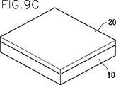
まず、図9(a)に示すように、低抵抗シリコンウエハ20とPyrex#7740などのガラス基板10に380℃で800Vを2時間加えて正極接合する。
【0046】
次に、図9(b)に示すように、水酸化カリウム(KOH)水溶液を使用してシリコンウエハ20をエッチングする。エッチング後、シリコンウエハ20の厚さは約70μm程度になるようにする。これは最終シリコン構造体の厚さである50μmにCMP(chemical mechanical polishing)を通じて鏡面を作るための余裕分20μmを勘案した厚さである。この時、エッチング液は80℃の36wt.%のKOH水溶液であり、この時のエッチング速度は大略0.93μm/minである。KOHエッチング後、シリコン表面にはヒルロック(hillock)及びピットホール(pithole)が形成される。
【0047】
次に、図9(c)に示すように、CMPを通じてシリコンウエハ20の表面を鏡面になるように作る。
【0048】
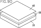
次に、図9(d)に示すように、フリップチップボンディングのための電極を形成するためにCrとAuを各々200Åと3000Åの厚さで蒸着してCr/Au層40を形成する。
【0049】
次に、図9(e)に示すように、Cr/Au層40上に酸化膜(図示せず)を蒸着して、その上に感光剤を塗布して、写真工程を行ってシリコン構造体パターンを定義するための感光剤パターン50を形成する。この時、感光剤パターンには、後にガラス基板をエッチングしてシリコン構造体を浮かべるために必要なエッチング液浸透用孔を形成するためのパターンが含まれている。
【0050】
次に、図9(f)に示すように、感光剤パターン50をエッチングマスクとして酸化膜をエッチングした後、感光剤パターン50と酸化膜パターンとをエッチングマスクとして反応性イオンエッチング(RIE: reactive ion etching)を進行してシリコン構造体パターンを形成する。シリコン構造体のパターンが形成されたシリコンウエハ20とガラス基板10は、ダイシング(dicing)して試片単位で分離する。
【0051】
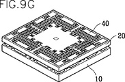
次に、図9(g)に示すように、シリコン構造体20をガラス基板10から分離するために、49%のHF溶液でガラス基板10をエッチングする。この時、既述したように、固定軸とスプリングの板を除いたシリコン構造体20の全ての部分には孔が形成され、エッチング液がガラス基板10に到達できるようになっている。この時、構造物をガラス基板から十分に浮かべて空気減衰(damping)を最少化しなければ、大気圧下で駆動するジャイロスコープを製作することができず、HF溶液を利用したガラスエッチングを利用すればガラス基板から10μm以上浮かんでいる構造物を製作することができる。この時、構造物をガラス基板から十分に浮かべて空気減衰(damping)を最少化しなければならない。約8分間ガラス基板10をエッチングすることにより、シリコン構造体20をガラス基板10から約50μm浮かんでいるようにすることができる。
【0052】
最後に、図9(h)に示すように、ガラス基板10、シリコン構造体20及びCr/Au層40からなるジャイロスコープ構造体200を配線のための電極構造物または PCB(printed circuit board)基板100にフリップチップボンディングする。この時、ボンダ(bonder)300はジャイロスコープ構造体200の固定軸部分に接触する。
【0053】
上記ではシリコン構造体のパターニング時のエッチングマスクとして感光剤と酸化膜を使用したが、感光剤だけを使用することもできる。
【0054】
以下、本発明のジャイロスコープの特徴について説明する。
【0055】
本発明によるジャイロスコープは非常に単純な工程に基づいて製作され、全工程でジャイロスコープ構造物を作るための写真エッチング工程は一回である。製作されたジャイロスコープは一つの構造物層だけを有するようになり、最終的にフリップチップボンディングを実行して回路部と連結される。
【0056】
ジャイロスコープ構造物の駆動部と検出部は、くし模様構造物を採用し、底面との間隔を大きくして空気減衰を最少化することによって、大気圧下でも高いQ値を有するように設計した。これは既存のジャイロスコープ設計では考慮されなかったQ値に対する数式を整理して、これに基づいて構造物のQ値を予測して機械的な感度を最大限になるように設計したものである。この時、Q値を予測するためにコウェッテフロー(Couette flow)、ストークスフロー(Stokes flow)とスクイズ減衰(Squeeze damping)が考慮されている。
【0057】
また、最大限の感度を得るために、与えられたジャイロスコープ領域内に最大限の電極構造物を集積して、10μm程度の大きな駆動変位を有するように設計しており、機械的な構造はジャイロスコープの機械的干渉を最少化して外部雑音に鈍感になるように設計されている。構造物の駆動及び検出周波数は外部雑音の影響を排除するために5kHzより大きく設計し、駆動と検出周波数は帯域幅をひろめるために一致させず、50Hz程度離れているように設計した。駆動及び検出周波数は各々7088Hz、7132Hzであると予測された。
【0058】
また、本発明のジャイロスコープの場合、人為的に変位を制限する変位制限装置(displacement limiter)がジャイロスコープについており、これは広い周波数範囲で駆動変位を一定に維持させて帯域幅をひろめて、チューニングの必要性を減らす役割を果たす。
【0059】
ジャイロスコープ構造物は基本的に2次元ステージ(2D stage、two dimensional stage)と同一の形態を有しており、同じ平面内で駆動モード及び検出モードが存在する。ジャイロスコープの感度は慣性質量(inertial mass)が大きいほど増加するので、これを勘案して、全体的なジャイロスコープの質量を大きくしなければならない。また、駆動力及び検出感度を最大にするために、構造物内でくし模様の電極構造物の数を最大にし、機械的な干渉を最少化するためにエッジジンバルを採択した。全体的なジャイロスコープ構造物の大きさは8×8[mm2]であり、密閉シーリング(hermetic sealing)のための外部フレームなどを考慮した全体大きさは10×10[mm2]である。構造物としては既述したように機械的性質に優れた単結晶シリコンを使用し、構造物の厚さは50μmに設計した。また、ジャイロスコープ構造物は減衰を減らすためにガラス基板から50μm浮かんでいる。
【0060】
前述したように、水平に振動する構造物の場合、Q値を計算するためには減衰値を計算しなければならず、一般に知られた減衰係数及びそれを計算する式は次の通りである。
【0061】
【数1】

ここでgは空気層の厚さであり、Aは球体の面積である。
【0063】
【数2】
ここで、δは透過深さで
【0065】
【数3】
と定義され、Aは構造体の面積である。
【0067】
【数4】
ここで、gは両板の間の空気層の厚さ、lは構造体の重み合わせた長さ、hは構造体の高さである。
【0069】
【数5】
【0070】
駆動部は426個のくし模様電極構造物を有し、6個の駆動用折りたたみスプリング(folded spring)構造物を有する。スプリングの長さを192μmとした時、スプリング係数は2684であり、駆動共振周波数は8299[Hz]で計算された。全体構造物の大きさを考慮して計算された大気圧でのQfactorは3565であり、駆動電圧を
【0071】
【数6】
【0072】
【数7】
【数8】
検出部は692個のくし模様電極構造物と6個の折りたたみスプリングを有する。スプリングの長さを157μmとした時、検出部の共振周波数は8269[Hz]で、駆動共振周波数に比べて多少小さい値を有するように設計した。検出部のQfactorは3765と計算された。この時、入力角速度によって発生するコリオリ力とそれに伴う変位は次のように計算される。
【0075】
【数9】
【数10】
したがって、ジャイロスコープの機械的感度は0.008[μm(/deg/sec)]であり、電気的な感度は1.939[fF/deg/sec]と計算された。
【0078】
本発明によるジャイロスコープの製作には一つの構造物層を有する工程を採択しており、そのために、深い反応性イオンエッチング(Deep RIE)工程とシリコン−ガラス正極接合工程を採択した。これを利用すると、一回のみの写真エッチング工程でジャイロスコープ構造物を製作することができ、電極基板及びPCBとのフリップチップボンディングによりジャイロスコープを完成することができる。
【0079】
Deep RIEエッチングマスクとして用いられた酸化膜は、オックスフォードエッチャー(Oxford Etcher)での酸化膜パターニング工程でアンダーカット(undercut)が発生しており、これがシリコン構造物に反映され、最終的に、Deep RIE後の構造物が設計した値より2μm程度狭く製作された。製作されたシリコン構造物の厚さは44μmであり、Deep RIEは33分間行った。シリコン構造体は8分間のガラスエッチング後、基板から完全にリリースされており、この時、基板と構造物との間隔は37μmと測定された。
【0080】
本発明によるジャイロスコープは426個の駆動電極と692個の検出電極を有し、駆動電極及び検出電極は慣性質量体によって機械的に分離された構造を有している。また、ジャイロスコープの慣性質量体の中央には変位を制限するための変位制限機があり、最大変位は15μmに制限される。また、機械的干渉をより減らすためのジンバル構造物を全体素子郊外周辺に配置した。
【0081】
製作された試片の性能を知るために、IRSC(半導体共同研究所)のプローブステーション(probe station)を利用して簡単な駆動性能を測定した。検出部の動作確認も駆動部と同様に電圧を印加して共振周波数及び共振点での最大変位を測定し、大略的な製作及び性能測定結果を表1に示す。
【0082】
【表1】
ここで、*印は印加電圧に対して計算された変位
【0084】
【数11】
【0085】
【数12】
を示す。
【0087】
23個の試片に対して電圧を印加して共振周波数を測定した結果、20個の試片が駆動部、検出部または駆動部及び検出部の動作確認に成功した。共振周波数は駆動及び検出共に5500〜6500Hzの範囲に幅広く分布していることが分かり、特に、5500〜6000Hzの領域に集中していることが確認できた。また、駆動部及び検出部の共振が確認された試片の場合、二つの共振周波数の差は大略50Hzで一定であることが確認できた。駆動部及び検出部のうちどちらか一方向への共振だけが観察された試片、あるいは、共振周波数の差が大きな試片の場合、スプリング部が破損していたり一方向への接着が発生していることが確認された。
【0088】
共振時の変位は前の表1のように実際の設計値より小さい値を示しており、これは単方向駆動による変位の減少、基板と構造物との間隔が設計より小さく製作されていることにより空気減衰が増加しQ値が減少したこと、及び、くし模様電極構造物のフッティング(footing)及びアンダーカット(undercut)によりくし模様電極間の間隔が増加したことにその原因があった。
【0089】
また、人為的に駆動電圧を増加させて変位制限装置の効用性を確認した。変位が変位制限装置によって制限される場合、数百Hzの範囲内で最大制限変位である15μmの駆動変位が維持されることが確認でき、これは外部雑音に左右されず、広い帯域幅を有することができることも確認できる。
【0090】
本発明は新たな形態の静電力駆動型、静電容量検出型角速度センサを提示する。単結晶シリコン微細加工技術を利用し、サイズの大きいジャイロスコープ構造物が製作できるようにすることによって、大気圧で動作可能なジャイロスコープを提示し、これを製作するためにシリコン−ガラス接合技術、シリコンエッチング技術とフリップチップボンディング技術を利用する。これは、一回のフォトリソグラフィ工程でエッチング孔(etch hole)を前面に有しているジャイロスコープ構造物を製作した後、追加的なフォトリソグラフィ工程なくガラスエッチングによって製作する非常に単純な工程である。特に、フリップチップボンディングを利用すれば、製作されたジャイロスコープ構造物をその他のパッケージ工程なく直ちに回路に集積化することができ、本ジャイロスコープは大気圧で動作可能であるので、既存のジャイロスコープが有している真空シーリング(sealing)工程の問題点を解決することができる。
【0091】
構造物は、大気圧でも大きな感度を有するように最大限に多くの駆動及び検出電極と最大限に大きな慣性質量体を有し、外部雑音の影響を排除するために高い周波数で大きな駆動動作変位を有するように設計される。ジャイロスコープ構造物は同じ平面内で駆動モード及び検出モードが存在するので、既存のジャイロスコープが有していた機械的干渉を排除することができる動作原理を採択し、外部にジンバル構造物を設置して機械的干渉を最少化する。また、駆動変位を制限する変位制限装置を機械的に追加して、付加的な周波数チューニングをしなくてもよい感度を有するようにジャイロスコープを設計し、ジャイロスコープの動作帯域幅が増えるように設計する。
【0092】
製作されたジャイロスコープは大気圧下で動作可能であり、意図した通りに大気圧下で大きな感度を有する。
【0093】
以上、本発明の最も実際的且つ好ましい実施例について説明したが、本発明は上述された実施例に限定されるものではなく、発明の目的及び特許請求の範囲内で多様に変形して実施することが可能であり、これらも本発明の範囲に属する。
【0094】
【図面の簡単な説明】
【図1】本発明の実施例によるジャイロスコープの斜視図である
【図2】本発明の実施例によるジャイロスコープの平面図である
【図3】図1の一部拡大図である
【図4】本発明の実施例によって製造されたジャイロスコープの部分SEM写真である
【図5】本発明の実施例によるジャイロスコープの駆動または検出スプリング部の拡大図である
【図6】本発明の実施例によって製造されたジャイロスコープの駆動または検出スプリング部のSEM写真である
【図7】本発明の実施例によるジャイロスコープの駆動または検出連結スプリング部の概念図である
【図8】変位制限部による共振駆動及び検出変位グラフである
【図9(a)】本発明の実施例によってジャイロスコープを製造する過程を示した図である
【図9(b)】本発明の実施例によってジャイロスコープを製造する過程を示した図である
【図9(c)】本発明の実施例によってジャイロスコープを製造する過程を示した図である
【図9(d)】本発明の実施例によってジャイロスコープを製造する過程を示した図である
【図9(e)】本発明の実施例によってジャイロスコープを製造する過程を示した図である
【図9(f)】本発明の実施例によってジャイロスコープを製造する過程を示した図である
【図9(g)】本発明の実施例によってジャイロスコープを製造する過程を示した図である
【図9(h)】本発明の実施例によってジャイロスコープを製造する過程を示した図である[0001]
Background of the Invention
(A) Technical field to which the invention belongs
The present invention relates to a gyroscope manufactured using a micromachining method and a manufacturing method thereof.
[0002]
(B) Conventional technology
Among various application fields using microfabrication, application to inertial sensors (Inertial sensors) has been an area of interest since early on. Research has been actively conducted to develop a commercial inertial sensor for the last ten years because of the advantage that an inertial sensor manufactured by microfabrication using silicon as a material is inexpensive, mass-produced, and can be integrated. However, a gyroscope of a level that can actually be commercialized has been produced and announced in recent years, and there is no example of a gyroscope manufactured by microfabrication yet commercialized. For commercialization, it is necessary to selectively detect low output values separately from noise with a wide operating range, and to acquire high sensitivity, and use a process that is completely compatible with existing semiconductor processes. However, it is necessary to implement a low-cost device using a simple process. Also, device reliability and high yield must be ensured.
[0003]
Analog Devices Inc. (ADI) developed a prototype of an integrated gyroscope that operates in vacuum using a surface micromachining process in 1998 with the goal of $ 30 per gyroscope in 1998. A gyroscope using a piezoelectric element is commercially available at a very low price of $ 15 for an automobile and $ 5 for a camera, so a new approach was required to compete with these. To that end, ADI worked to develop a low-cost gyroscope by miniaturizing the device and minimizing the packaging process. To reduce the size of the device, reduce the circuit portion that occupies most of the total device size, solve the problem by enlarging the mechanical part of the gyroscope, and seek the direction to reduce the overall device size It became so. In addition, if the machine part is large, it can be operated even with a relatively low Q value, and it can be considered that two goals for commercialization, that is, removal of a small-sized element and a vacuum package can be satisfied. In the case of elements that must actually be vacuum packaged, the package ratio in the general IC process occupies a large price ratio of 80% compared to 50%. This is necessary to reduce the price of all devices.
[0004]
Summary of the Invention
A technical problem to be solved by the present invention is to provide a gyroscope that can operate at atmospheric pressure.
[0005]
Another technical problem of the present invention is to provide a gyroscope having a large driving displacement at a high frequency.
[0006]
Another technical problem to be solved by the present invention is to provide a gyroscope in which mechanical interference between the drive mode and the detection mode is eliminated.
[0007]
Another technical problem to be solved by the present invention is to provide a gyroscope that exhibits high sensitivity without frequency tuning.
[0008]
Another technical problem to be solved by the present invention is to simplify the manufacturing method of the gyroscope.
[0009]
In order to solve such problems, the present invention eliminates mechanical interference between the drive displacement electrode and the detection displacement electrode by connecting the drive displacement electrode and the detection displacement electrode through an inertia mass body and a folding spring as a medium. To do.
[0010]
Specifically, a gyroscope as one aspect of the present invention is connected to a fixed driving fixed electrode, a driving displacement electrode that can be displaced in the first direction by a counter electrode of the driving fixed electrode, and the driving displacement electrode. The inertial mass body that is displaced in the first direction along the displacement in the first direction of the drive displacement electrode and is displaced in the second direction when the angular velocity is applied, is connected to the inertial mass body and is displaced in the second direction of the inertial mass body. And a detection fixed electrode fixed by a counter electrode of the detection displacement electrode.
[0011]
At this time, the drive displacement electrode is supported by a folding spring that can move in the first direction, and the detection displacement electrode is supported by a folding spring that can move in the second direction.
[0012]
The drive displacement electrode and the inertial mass body can be moved in the second direction and are connected by a folding spring without a fixed shaft, and the detection displacement electrode and the inertial mass body can be moved in the first direction. They are connected by a folding spring without a fixed shaft.
[0013]
In addition, two detection displacement electrodes are arranged on both sides around the inertial mass body, and the gyroscope can further include an edge gimbal connecting the two detection displacement electrodes, and there is a hole in the center of the inertial mass body. , And may further include a displacement limiting shaft positioned and fixed at the center of the hole.
[0014]
In addition, it may further include a tuning electrode that is formed symmetrically on both sides of the detection displacement electrode and adjusts the detection sensitivity by changing the resonance frequency of the detection displacement electrode by acting as an electrical spring.
[0015]
Such a gyroscope includes: (a) a step of positively bonding a silicon substrate and a glass substrate; (b) a step of etching and polishing the silicon substrate to obtain a specific thickness; and (c) a metal on the silicon substrate. Forming a layer; (d) forming a silicon structure having a gyroscope pattern by photolithography of the metal layer and the silicon substrate; and (e) etching the glass substrate to form the silicon structure. Out ofpluralSeparate the remaining part from the glass substrate except the fixed shaftThe driving fixed electrode fixed by the fixed shaft, the counter electrode of the driving fixed electrode, the driving displacement electrode capable of being displaced in the first direction, and the driving displacement electrode The inertial mass body that is displaced in the first direction along the displacement in the first direction of the drive displacement electrode and that is displaced in the second direction when the angular velocity is applied is coupled to the inertial mass body. A detection displacement electrode that can be displaced in a second direction along a two-direction displacement; and a detection fixed electrode that is opposed to the detection displacement electrode and is fixed by the fixed shaft. The detection displacement electrode is supported by a folding spring that can move in a first direction, the detection displacement electrode is supported by a folding spring that can move in a second direction, and the drive displacement electrode and the inertial mass body. Can move in the second direction and is connected by a folding spring without the fixed shaft, and the detection displacement electrode and the inertial mass body can move in the first direction without the fixed shaft. Connected by folding springForming a gyroscope structure; and (f) flip-chip bonding the gyroscope structure to connect to an external circuit.
[0016]
At this time, the method may further include a step of dicing the silicon substrate and the glass substrate between (d) and (e) to separate them into individual device units.
[0017]
The metal layer formed in (c) is preferably a double layer of Cr and Au, and in (e) the glass substrate is etched using an HF solution.
[0018]
Etch depth of the glass substrate using HF solution is 10 μm or more to minimize air attenuation and allow the gyroscope to operate at atmospheric pressure.
[0019]
In (b), the silicon substrate was etched at 36 wt. It is preferred to use a 1% aqueous KOH solution.
[0020]
Brief Description of Drawings
For a full understanding of the structure of the detailed portions of the embodiments of the present invention, reference is made to the accompanying drawings.
FIG. 1 is a perspective view of a gyroscope according to an embodiment of the present invention.
FIG. 2 is a plan view of a gyroscope according to an embodiment of the present invention.
FIG. 3 is a partially enlarged view of FIG.
FIG. 4 is a partial SEM photograph of a gyroscope manufactured according to an embodiment of the present invention.
FIG. 5 is an enlarged view of a drive or detection spring portion of a gyroscope according to an embodiment of the present invention.
FIG. 6 is an SEM photograph of a drive or detection spring portion of a gyroscope manufactured according to an embodiment of the present invention.
FIG. 7 is a conceptual diagram of a drive or detection connecting spring portion of a gyroscope according to an embodiment of the present invention.
FIG. 8 is a resonance drive and detected displacement graph by the displacement limiting unit.
FIGS. 9A to 9H are views showing a process of manufacturing a gyroscope according to an embodiment of the present invention.
[0021]
Detailed description of the preferred embodiment
In the following, a detailed description of a preferred embodiment of the present invention is given, and an optimal method for carrying out the invention carried out by the inventor is shown. As described above, the present invention can be variously modified and implemented without departing from the invention, and is not limited to the description and drawings described above.
[0022]
1 is a perspective view of a gyroscope according to an embodiment of the present invention, FIG. 2 is a plan view of the gyroscope according to an embodiment of the present invention, FIG. 3 is a partially enlarged view of FIG. 1, and FIG. 2 is a partial SEM (Scanning Electron Microscope) photograph of the gyroscope manufactured according to the embodiment of FIG.
[0023]
A gyroscope according to an embodiment of the present invention includes a
[0024]
The silicon structure includes a drive unit, a detection unit, a large number of springs, a tuning
[0025]
Hereinafter, the structure and function of each of these elements will be described in more detail.
[0026]
First, the driving fixed
[0027]
Next, the detection fixed
[0028]
Four
[0029]
The
[0030]
A method for driving and detecting the gyroscope having such a structure will be described.
[0031]
When power is applied to the drive fixed
[0032]
The structure of the drive or detection springs 27, 28, 29, 30 applied to the embodiment of the present invention will be described in more detail with reference to FIGS.
[0033]
FIG. 5 is a conceptual diagram of a drive or detection spring part of a gyroscope according to an embodiment of the present invention, and FIG. 6 is an SEM photograph of a drive or detection spring part of a gyroscope manufactured according to an embodiment of the present invention.
[0034]
The drive or detection spring includes a fixed shaft 1, a connecting
[0035]
In FIG. 5, the layer displayed thinly on the silicon structure is a metal layer. This metal layer is formed for flip chip bonding of the gyroscope. The illustration is omitted in FIGS. 1 to 4.
[0036]
In FIG. 6, the holes formed in the periphery of the connecting
[0037]
The structure of the drive or detection coupling springs 31 and 32 applied to the embodiment of the present invention will be described in more detail with reference to FIG.
[0038]
FIG. 7 is a conceptual diagram of a drive or detection connecting spring portion of a gyroscope according to an embodiment of the present invention.
[0039]
The connecting spring is composed of the connecting
[0040]
Next, the function of the displacement limiting unit will be described.
[0041]
FIG. 8 is a resonance drive and detected displacement graph by the displacement limiting unit.
[0042]
In the case of a resonant structure with a high Q value, the displacement change due to the change in the degree of vacuum and frequency is very large, and this changes the output of the structure. Therefore, the output performance is greatly affected by external noise (change in vacuum degree and frequency). There is a disadvantage that becomes sensitive. In order to overcome this, the present gyroscope forms a mechanical displacement limiting device for limiting the drive displacement at the center of the inertial mass body. This maintains the displacement of the drive unit including the inertial mass body at a constant value, and maintains a constant displacement even in a wide frequency range. Further, as shown in FIG. 8, in the case of an existing gyroscope, when a difference in driving and detection resonance frequency occurs due to a process error, the resonance frequency must be tuned to prevent the sensitivity from being lowered. However, in the case of this gyroscope adopting the displacement limiting device, the driving displacement is kept constant in a wide frequency range, and the driving displacement is kept constant even in the detection resonance frequency range. It can be driven at the detected resonance frequency.
[0043]
Hereinafter, a method for manufacturing the gyroscope having the above structure will be described.
[0044]
FIGS. 9A to 9H are perspective views sequentially illustrating a process of manufacturing a gyroscope according to an embodiment of the present invention.
[0045]
First, as shown in FIG. 9A, a low-
[0046]
Next, as shown in FIG. 9B, the
[0047]
Next, as shown in FIG. 9C, the surface of the
[0048]
Next, as shown in FIG. 9 (d), Cr and Au are vapor-deposited to a thickness of 200 mm and 3000 mm, respectively, in order to form an electrode for flip chip bonding to form a Cr /
[0049]
Next, as shown in FIG. 9 (e), an oxide film (not shown) is vapor-deposited on the Cr /
[0050]
Next, as shown in FIG. 9F, after the oxide film is etched using the
[0051]
Next, as shown in FIG. 9G, the
[0052]
Finally, as shown in FIG. 9 (h), a
[0053]
In the above description, the photosensitive agent and the oxide film are used as the etching mask for patterning the silicon structure. However, only the photosensitive agent can be used.
[0054]
Hereinafter, features of the gyroscope of the present invention will be described.
[0055]
The gyroscope according to the present invention is manufactured based on a very simple process, and the photo-etching process for making the gyroscope structure in one process is one time. The manufactured gyroscope has only one structure layer and is finally connected to the circuit unit by performing flip chip bonding.
[0056]
The drive part and the detection part of the gyroscope structure are designed to have a high Q value even under atmospheric pressure by adopting a comb pattern structure and increasing the distance from the bottom surface to minimize air attenuation. . This is a system designed to maximize the mechanical sensitivity by organizing mathematical formulas for Q values that were not considered in existing gyroscope designs and predicting the Q values of structures based on this formula. . At this time, the Couette flow, Stokes flow, and Squeeze damping are considered in order to predict the Q value.
[0057]
Moreover, in order to obtain the maximum sensitivity, the maximum electrode structure is integrated in a given gyroscope region and designed to have a large driving displacement of about 10 μm. Designed to minimize gyroscope mechanical interference and be insensitive to external noise. The drive and detection frequencies of the structure were designed to be greater than 5 kHz in order to eliminate the influence of external noise, and the drive and detection frequencies were designed to be about 50 Hz apart from each other in order to widen the bandwidth. The drive and detection frequencies were predicted to be 7088 Hz and 7132 Hz, respectively.
[0058]
In addition, in the case of the gyroscope of the present invention, a displacement limiter that artificially limits the displacement is attached to the gyroscope, which maintains the driving displacement constant in a wide frequency range and widens the bandwidth, It serves to reduce the need for tuning.
[0059]
The gyroscope structure basically has the same form as a two-dimensional stage (2D stage), and a drive mode and a detection mode exist in the same plane. Since the sensitivity of the gyroscope increases as the inertial mass increases, the overall mass of the gyroscope must be increased in consideration of this. In order to maximize driving force and detection sensitivity, an edge gimbal was adopted to maximize the number of comb-shaped electrode structures in the structure and to minimize mechanical interference. Overall gyroscope structure size is 8x8 [mm2The overall size is 10 x 10 [mm] considering the outer frame for hermetic sealing.2]. As described above, single crystal silicon having excellent mechanical properties was used as described above, and the thickness of the structure was designed to be 50 μm. Also, the gyroscope structure floats 50 μm from the glass substrate to reduce attenuation.
[0060]
As described above, in the case of a structure that vibrates horizontally, in order to calculate the Q value, the attenuation value must be calculated. The generally known attenuation coefficient and the equation for calculating the attenuation coefficient are as follows. .
[0061]
[Expression 1]
Where g is the thickness of the air layer and A is the area of the sphere.
[0063]
[Expression 2]
Where δ is the penetration depth
[0065]
[Equation 3]
A is the area of the structure.
[0067]
[Expression 4]
Here, g is the thickness of the air layer between both plates, l is the weighted length of the structure, and h is the height of the structure.
[0069]
[Equation 5]
[0070]
The driving unit has 426 comb-shaped electrode structures, and 6 driving folded spring structures. When the length of the spring was 192 μm, the spring coefficient was 2684, and the drive resonance frequency was calculated at 8299 [Hz]. The Qfactor at atmospheric pressure calculated in consideration of the size of the entire structure is 3565, and the driving voltage is
[0071]
[Formula 6]
[0072]
[Expression 7]
[Equation 8]
The detection unit has 692 comb-shaped electrode structures and six folding springs. When the length of the spring is 157 μm, the resonance frequency of the detection unit is 8269 [Hz], which is designed to be slightly smaller than the drive resonance frequency. The Qfactor of the detection unit was calculated as 3765. At this time, the Coriolis force generated by the input angular velocity and the displacement accompanying it are calculated as follows.
[0075]
[Equation 9]
[Expression 10]
Therefore, the mechanical sensitivity of the gyroscope was 0.008 [μm (/ deg / sec)], and the electrical sensitivity was calculated to be 1.939 [fF / deg / sec].
[0078]
In order to manufacture the gyroscope according to the present invention, a process having one structure layer is adopted. For this purpose, a deep reactive ion etching (Deep RIE) process and a silicon-glass cathode bonding process are adopted. If this is utilized, a gyroscope structure can be manufactured by only one photo etching process, and a gyroscope can be completed by flip chip bonding with an electrode substrate and PCB.
[0079]
In the oxide film used as a deep RIE etching mask, an undercut occurs in the oxide film patterning process in Oxford Etcher, which is reflected in the silicon structure, and finally, deep RIE. The latter structure was manufactured to be about 2 μm narrower than the designed value. The fabricated silicon structure had a thickness of 44 μm, and Deep RIE was performed for 33 minutes. The silicon structure was completely released from the substrate after 8 minutes of glass etching. At this time, the distance between the substrate and the structure was measured to be 37 μm.
[0080]
The gyroscope according to the present invention has 426 drive electrodes and 692 detection electrodes, and the drive electrodes and the detection electrodes have a structure mechanically separated by an inertial mass body. There is a displacement limiter for limiting the displacement at the center of the inertial mass body of the gyroscope, and the maximum displacement is limited to 15 μm. In addition, a gimbal structure for further reducing mechanical interference was arranged around the entire element.
[0081]
In order to know the performance of the manufactured specimen, a simple driving performance was measured by using a probe station of IRSC (Semiconductor Joint Laboratory). As for the operation check of the detection unit, a voltage is applied to measure the maximum displacement at the resonance frequency and resonance point in the same manner as the drive unit.
[0082]
[Table 1]
here,*Is the displacement calculated for the applied voltage
[0084]
## EQU11 ##
[0085]
[Expression 12]
Indicates.
[0087]
As a result of applying a voltage to 23 specimens and measuring the resonance frequency, 20 specimens succeeded in confirming the operation of the drive unit, the detection unit, or the drive unit and the detection unit. It was found that the resonance frequency was widely distributed in the range of 5500 to 6500 Hz for both driving and detection, and in particular, it was confirmed that it was concentrated in the region of 5500 to 6000 Hz. Further, in the case of the specimen in which the resonance of the drive unit and the detection unit was confirmed, it was confirmed that the difference between the two resonance frequencies was substantially constant at 50 Hz. In the case of a specimen in which only resonance in one direction is observed among the drive part and the detection part, or a specimen having a large difference in resonance frequency, the spring part is damaged or adhesion in one direction occurs. It was confirmed that
[0088]
The displacement at resonance shows a value smaller than the actual design value as shown in Table 1 above. This is because the displacement is reduced by the unidirectional drive and the distance between the substrate and the structure is made smaller than the design. The cause of this was that the air attenuation increased and the Q value decreased due to the above, and the spacing between the comb pattern electrodes increased due to footing and undercut of the comb pattern electrode structure.
[0089]
In addition, the utility of the displacement limiting device was confirmed by artificially increasing the drive voltage. When the displacement is limited by the displacement limiting device, it can be confirmed that the driving displacement of 15 μm which is the maximum limiting displacement is maintained within a range of several hundred Hz, which is not influenced by external noise and has a wide bandwidth. It can also be confirmed that it is possible.
[0090]
The present invention presents a new form of electrostatic force drive type, capacitance detection type angular velocity sensor. By using single-crystal silicon microfabrication technology, a gyroscope capable of operating at atmospheric pressure is presented by making it possible to produce a gyroscope structure with a large size, and silicon-glass bonding technology for producing this gyroscope, Utilize silicon etching technology and flip chip bonding technology. This is a very simple process in which a gyroscope structure having an etch hole on the front surface is manufactured by a single photolithography process, and then manufactured by glass etching without an additional photolithography process. is there. In particular, if flip-chip bonding is used, the manufactured gyroscope structure can be immediately integrated into a circuit without any other packaging process, and this gyroscope can operate at atmospheric pressure. Can solve the problems of the vacuum sealing process.
[0091]
The structure has a maximum number of drive and detection electrodes and a maximum inertia mass so as to have a large sensitivity even at atmospheric pressure, and a large drive operation displacement at high frequency to eliminate the influence of external noise Designed to have Since the gyroscope structure has a drive mode and a detection mode in the same plane, the operation principle that can eliminate the mechanical interference that the existing gyroscope had was adopted, and the gimbal structure was installed outside To minimize mechanical interference. In addition, a gyroscope is designed to have a sensitivity that does not require additional frequency tuning by mechanically adding a displacement limiting device that limits the drive displacement so that the operating bandwidth of the gyroscope increases. design.
[0092]
The manufactured gyroscope can operate under atmospheric pressure, and has great sensitivity under atmospheric pressure as intended.
[0093]
Although the most practical and preferred embodiments of the present invention have been described above, the present invention is not limited to the above-described embodiments, and various modifications may be made within the scope of the invention and the scope of the claims. These are also within the scope of the present invention.
[0094]
[Brief description of the drawings]
FIG. 1 is a perspective view of a gyroscope according to an embodiment of the present invention.
FIG. 2 is a plan view of a gyroscope according to an embodiment of the present invention.
FIG. 3 is a partially enlarged view of FIG.
FIG. 4 is a partial SEM photograph of a gyroscope manufactured according to an embodiment of the present invention.
FIG. 5 is an enlarged view of a drive or detection spring portion of a gyroscope according to an embodiment of the present invention.
FIG. 6 is an SEM photograph of a drive or detection spring portion of a gyroscope manufactured according to an embodiment of the present invention.
FIG. 7 is a conceptual diagram of a drive or detection connecting spring portion of a gyroscope according to an embodiment of the present invention.
FIG. 8 is a resonance drive and detected displacement graph by a displacement limiting unit.
FIG. 9A is a diagram showing a process of manufacturing a gyroscope according to an embodiment of the present invention.
FIG. 9B is a diagram showing a process of manufacturing a gyroscope according to an embodiment of the present invention.
FIG. 9 (c) is a view showing a process of manufacturing a gyroscope according to an embodiment of the present invention.
FIG. 9D is a diagram showing a process of manufacturing a gyroscope according to an embodiment of the present invention.
FIG. 9 (e) is a diagram showing a process of manufacturing a gyroscope according to an embodiment of the present invention.
FIG. 9 (f) is a view showing a process of manufacturing a gyroscope according to an embodiment of the present invention.
FIG. 9G is a view showing a process of manufacturing a gyroscope according to an embodiment of the present invention.
FIG. 9 (h) is a view showing a process of manufacturing a gyroscope according to an embodiment of the present invention.
Claims (12)
前記駆動固定電極の対向電極であって、第1方向への変位が可能な駆動変位電極と、
前記駆動変位電極に連結されており、前記駆動変位電極の第1方向変位に沿って第1方向に変位し、角速度印加時に第2方向に変位する慣性質量体と、
前記慣性質量体に連結されており、前記慣性質量体の第2方向変位に沿って第2方向に変位することができる検出変位電極と、
前記検出変位電極の対向電極で、固定されている検出固定電極と、を含み、
前記駆動変位電極は第1方向に移動することができる折りたたみスプリングによって支持されており、前記検出変位電極は第2方向に移動できる折りたたみスプリングによって支持され、
前記駆動変位電極と前記慣性質量体とは第2方向に移動することができ、固定軸のない折りたたみスプリングによって連結されており、前記検出変位電極と前記慣性質量体とは第1方向に移動することができ、固定軸のない折りたたみスプリングによって連結されているジャイロスコープ。A fixed driving fixed electrode;
A drive displacement electrode that is a counter electrode of the drive fixed electrode and capable of displacement in a first direction;
An inertial mass connected to the drive displacement electrode, displaced in a first direction along a first direction displacement of the drive displacement electrode, and displaced in a second direction when an angular velocity is applied;
A detection displacement electrode coupled to the inertial mass body and capable of being displaced in a second direction along a second direction displacement of the inertial mass body;
In the counter electrode of the detection displacement electrode, it viewed including the detection fixed electrode is fixed, and
The drive displacement electrode is supported by a folding spring that can move in a first direction, and the detection displacement electrode is supported by a folding spring that can move in a second direction;
The drive displacement electrode and the inertial mass body can move in the second direction and are connected by a folding spring without a fixed shaft, and the detection displacement electrode and the inertial mass body move in the first direction. A gyroscope that can be connected by a folding spring without a fixed shaft .
(b)前記シリコン基板をエッチング及び研磨して特定の厚さに作る段階と、
(c)前記シリコン基板上に金属層を形成する段階と、
(d)前記金属層と前記シリコン基板とをフォトリソグラフィによりジャイロスコープパターンを有するシリコン構造体に形成する段階と、
(e)前記ガラス基板をエッチングし、前記シリコン構造体のうち複数の固定軸を除いた残りの部分をガラス基板から分離して、前記固定軸によって固定されている駆動固定電極と、前記駆動固定電極の対向電極であって、第1方向への変位が可能な駆動変位電極と、前記駆動変位電極に連結されており、前記駆動変位電極の第1方向変位に沿って第1方向に変位し、角速度印加時に第2方向に変位する慣性質量体と、前記慣性質量体に連結されており、前記慣性質量体の第2方向変位に沿って第2方向に変位することができる検出変位電極と、前記検出変位電極の対向電極で、前記固定軸によって固定されている検出固定電極と、を含み、前記駆動変位電極は第1方向に移動することができる折りたたみスプリングによって支持されており、前記検出変位電極は第2方向に移動できる折りたたみスプリングによって支持され、前記駆動変位電極と前記慣性質量体とは第2方向に移動することができ、前記固定軸のない折りたたみスプリングによって連結されており、前記検出変位電極と前記慣性質量体とは第1方向に移動することができ、前記固定軸のない折りたたみスプリングによって連結されているジャイロスコープ構造体を形成する段階と、
(f)前記ジャイロスコープ構造体をフリップチップボンディングして外部回路と連結する段階と、を含むジャイロスコープの製造方法。(A) positively bonding a silicon substrate and a glass substrate;
(B) etching and polishing the silicon substrate to a specific thickness;
(C) forming a metal layer on the silicon substrate;
Forming a silicon structure having a gyroscope pattern by; (d) silicon substrate and the photolithography and the metal layer,
(E) etching the glass substrate, separating the remaining part of the silicon structure excluding a plurality of fixed shafts from the glass substrate, and driving fixed electrodes fixed by the fixed shaft; A driving displacement electrode that is a counter electrode of the electrode and is capable of displacement in a first direction, and is connected to the driving displacement electrode, and is displaced in the first direction along the first direction displacement of the driving displacement electrode. An inertial mass body that is displaced in the second direction when the angular velocity is applied, and a detection displacement electrode that is connected to the inertial mass body and can be displaced in the second direction along the second direction displacement of the inertial mass body; A detection fixed electrode fixed by the fixed shaft at a counter electrode of the detection displacement electrode, and the drive displacement electrode is supported by a folding spring that can move in the first direction. The detection displacement electrode is supported by a folding spring that can move in the second direction, and the drive displacement electrode and the inertial mass body can move in the second direction and are connected by a folding spring without the fixed shaft. Forming a gyroscope structure in which the detection displacement electrode and the inertial mass can move in a first direction and are connected by a folding spring without the fixed shaft ;
And (f) a step of flip chip bonding the gyroscope structure and connecting the gyroscope structure to an external circuit.
Applications Claiming Priority (2)
| Application Number | Priority Date | Filing Date | Title |
|---|---|---|---|
| KR10-2001-0006695A KR100418624B1 (en) | 2001-02-12 | 2001-02-12 | a gyroscope and a manufacturing method of the same |
| PCT/KR2002/000135 WO2002064497A1 (en) | 2001-02-12 | 2002-01-30 | Gyroscope and fabrication method thereof |
Publications (3)
| Publication Number | Publication Date |
|---|---|
| JP2004518964A JP2004518964A (en) | 2004-06-24 |
| JP2004518964A5 JP2004518964A5 (en) | 2005-01-27 |
| JP3713019B2 true JP3713019B2 (en) | 2005-11-02 |
Family
ID=19705617
Family Applications (1)
| Application Number | Title | Priority Date | Filing Date |
|---|---|---|---|
| JP2002564435A Expired - Fee Related JP3713019B2 (en) | 2001-02-12 | 2002-01-30 | Gyroscope and manufacturing method thereof |
Country Status (8)
| Country | Link |
|---|---|
| US (1) | US6845668B2 (en) |
| EP (1) | EP1360144B1 (en) |
| JP (1) | JP3713019B2 (en) |
| KR (1) | KR100418624B1 (en) |
| CN (1) | CN1242913C (en) |
| AT (1) | ATE414674T1 (en) |
| DE (1) | DE60229919D1 (en) |
| WO (1) | WO2002064497A1 (en) |
Families Citing this family (26)
| Publication number | Priority date | Publication date | Assignee | Title |
|---|---|---|---|---|
| US7037805B2 (en) | 2003-05-07 | 2006-05-02 | Honeywell International Inc. | Methods and apparatus for attaching a die to a substrate |
| US6927098B2 (en) * | 2003-05-07 | 2005-08-09 | Honeywell International Inc. | Methods and apparatus for attaching MEMS devices to housing |
| SG112898A1 (en) * | 2003-12-11 | 2005-07-28 | Singapore Tech Dynamics Pte | Sensing apparatus, system and method |
| JP2005326620A (en) * | 2004-05-14 | 2005-11-24 | Fujitsu Ltd | Micromirror element |
| CN100338470C (en) * | 2005-03-25 | 2007-09-19 | 中北大学 | Single chip double inertia parameter accelerometer gyroscope |
| JP5070778B2 (en) * | 2006-09-20 | 2012-11-14 | 株式会社デンソー | Mechanical quantity sensor |
| US8061201B2 (en) * | 2007-07-13 | 2011-11-22 | Georgia Tech Research Corporation | Readout method and electronic bandwidth control for a silicon in-plane tuning fork gyroscope |
| US8776601B2 (en) | 2010-11-23 | 2014-07-15 | Honeywell International Inc. | MEMS sensor using multi-layer movable combs |
| US8748206B2 (en) | 2010-11-23 | 2014-06-10 | Honeywell International Inc. | Systems and methods for a four-layer chip-scale MEMS device |
| US9493344B2 (en) | 2010-11-23 | 2016-11-15 | Honeywell International Inc. | MEMS vertical comb structure with linear drive/pickoff |
| US9171964B2 (en) | 2010-11-23 | 2015-10-27 | Honeywell International Inc. | Systems and methods for a three-layer chip-scale MEMS device |
| CN102507981B (en) * | 2011-11-02 | 2013-06-05 | 重庆理工大学 | Single-sensitive-mass-element silicon micro-two-dimensional acceleration transducer with coupled beam structure |
| CN102633227B (en) * | 2012-03-16 | 2014-07-23 | 中北大学 | Film pressure damp adjustable device for MEMS (micro-electromechanical system) inertial sensor structure |
| US9581447B2 (en) * | 2014-07-08 | 2017-02-28 | Honeywell International Inc. | MEMS gyro motor loop filter |
| US9903718B2 (en) * | 2015-05-28 | 2018-02-27 | Invensense, Inc. | MEMS device mechanical amplitude control |
| US10514259B2 (en) | 2016-08-31 | 2019-12-24 | Analog Devices, Inc. | Quad proof mass MEMS gyroscope with outer couplers and related methods |
| US10627235B2 (en) | 2016-12-19 | 2020-04-21 | Analog Devices, Inc. | Flexural couplers for microelectromechanical systems (MEMS) devices |
| US10415968B2 (en) | 2016-12-19 | 2019-09-17 | Analog Devices, Inc. | Synchronized mass gyroscope |
| US10697774B2 (en) | 2016-12-19 | 2020-06-30 | Analog Devices, Inc. | Balanced runners synchronizing motion of masses in micromachined devices |
| FR3065800B1 (en) * | 2017-04-27 | 2019-08-02 | Safran | CONFIGURED RESONATOR TO BE INTEGRATED WITH INERTIAL ANGULAR SENSOR |
| US10948294B2 (en) | 2018-04-05 | 2021-03-16 | Analog Devices, Inc. | MEMS gyroscopes with in-line springs and related systems and methods |
| US11193771B1 (en) | 2020-06-05 | 2021-12-07 | Analog Devices, Inc. | 3-axis gyroscope with rotational vibration rejection |
| WO2021252398A1 (en) | 2020-06-08 | 2021-12-16 | Analog Devices, Inc. | Drive and sense stress relief apparatus |
| WO2021252364A1 (en) | 2020-06-08 | 2021-12-16 | Analog Devices, Inc. | Stress-relief mems gyroscope |
| US11698257B2 (en) | 2020-08-24 | 2023-07-11 | Analog Devices, Inc. | Isotropic attenuated motion gyroscope |
| CN113135548A (en) * | 2021-04-20 | 2021-07-20 | 广州蜂鸟传感科技有限公司 | Piezoelectric micro-mechanical actuator |
Family Cites Families (7)
| Publication number | Priority date | Publication date | Assignee | Title |
|---|---|---|---|---|
| DE19530007C2 (en) * | 1995-08-16 | 1998-11-26 | Bosch Gmbh Robert | Yaw rate sensor |
| US5945599A (en) * | 1996-12-13 | 1999-08-31 | Kabushiki Kaisha Toyota Chuo Kenkyusho | Resonance type angular velocity sensor |
| US5914521A (en) * | 1997-07-30 | 1999-06-22 | Motorola, Inc. | Sensor devices having a movable structure |
| US6122961A (en) * | 1997-09-02 | 2000-09-26 | Analog Devices, Inc. | Micromachined gyros |
| KR100231715B1 (en) | 1997-11-25 | 1999-11-15 | 정선종 | Planer vibratory microgyroscope |
| KR100316774B1 (en) | 1999-01-15 | 2001-12-12 | 이형도 | Method for fabricating a micro inertia sensor |
| WO2000068640A2 (en) | 1999-04-21 | 2000-11-16 | The Regents Of The University Of California | Micro-machined angle-measuring gyroscope |
-
2001
- 2001-02-12 KR KR10-2001-0006695A patent/KR100418624B1/en active IP Right Grant
-
2002
- 2002-01-30 EP EP02711501A patent/EP1360144B1/en not_active Expired - Lifetime
- 2002-01-30 DE DE60229919T patent/DE60229919D1/de not_active Expired - Fee Related
- 2002-01-30 JP JP2002564435A patent/JP3713019B2/en not_active Expired - Fee Related
- 2002-01-30 CN CNB028002954A patent/CN1242913C/en not_active Expired - Fee Related
- 2002-01-30 AT AT02711501T patent/ATE414674T1/en not_active IP Right Cessation
- 2002-01-30 WO PCT/KR2002/000135 patent/WO2002064497A1/en active Application Filing
- 2002-01-30 US US10/257,532 patent/US6845668B2/en not_active Expired - Fee Related
Also Published As
| Publication number | Publication date |
|---|---|
| US6845668B2 (en) | 2005-01-25 |
| WO2002064497A1 (en) | 2002-08-22 |
| US20030159509A1 (en) | 2003-08-28 |
| EP1360144B1 (en) | 2008-11-19 |
| DE60229919D1 (en) | 2009-01-02 |
| CN1457319A (en) | 2003-11-19 |
| ATE414674T1 (en) | 2008-12-15 |
| KR100418624B1 (en) | 2004-02-11 |
| CN1242913C (en) | 2006-02-22 |
| EP1360144A1 (en) | 2003-11-12 |
| JP2004518964A (en) | 2004-06-24 |
| KR20020066486A (en) | 2002-08-19 |
Similar Documents
| Publication | Publication Date | Title |
|---|---|---|
| JP3713019B2 (en) | Gyroscope and manufacturing method thereof | |
| US7621183B2 (en) | X-Y axis dual-mass tuning fork gyroscope with vertically integrated electronics and wafer-scale hermetic packaging | |
| KR101105059B1 (en) | Method of making an x-y axis dual-mass tuning fork gyroscope with vertically integrated electronics and wafer-scale hermetic packaging | |
| JP5123455B2 (en) | Microfabricated tuning fork gyroscope and associated triaxial inertial measurement system for detecting out-of-plane rotation | |
| US7250112B2 (en) | Method of making an X-Y axis dual-mass tuning fork gyroscope with vertically integrated electronics and wafer-scale hermetic packaging | |
| JP5450451B2 (en) | XY Axis Dual Mass Tuning Fork Gyroscope with Vertically Integrated Electronic Circuits and Wafer Scale Sealed Packaging | |
| US6892575B2 (en) | X-Y axis dual-mass tuning fork gyroscope with vertically integrated electronics and wafer-scale hermetic packaging | |
| JP3950925B2 (en) | Micromechanical rotational speed sensor | |
| US7640803B1 (en) | Micro-electromechanical system inertial sensor | |
| JPH11505021A (en) | Vibratory gyroscope with gimbal-supported strain relief | |
| US9273962B2 (en) | Physical quantity sensor and electronic device | |
| EP2006636A2 (en) | Angular velocity detecting device | |
| US20230314469A1 (en) | Mems tri-axial accelerometer with one or more decoupling elements | |
| JP2007333642A (en) | Inertia sensor and method for manufacturing inertia sensor | |
| KR19990042067A (en) | Planar Vibration Micro Gyroscope | |
| KR101459797B1 (en) | Rotation type of gyroscope | |
| JPS60113105A (en) | Oscillation-type angular velocity meter |
Legal Events
| Date | Code | Title | Description |
|---|---|---|---|
| A131 | Notification of reasons for refusal |
Free format text: JAPANESE INTERMEDIATE CODE: A131 Effective date: 20050217 |
|
| A521 | Request for written amendment filed |
Free format text: JAPANESE INTERMEDIATE CODE: A523 Effective date: 20050517 |
|
| TRDD | Decision of grant or rejection written | ||
| A01 | Written decision to grant a patent or to grant a registration (utility model) |
Free format text: JAPANESE INTERMEDIATE CODE: A01 Effective date: 20050804 |
|
| A61 | First payment of annual fees (during grant procedure) |
Free format text: JAPANESE INTERMEDIATE CODE: A61 Effective date: 20050818 |
|
| R150 | Certificate of patent or registration of utility model |
Free format text: JAPANESE INTERMEDIATE CODE: R150 |
|
| FPAY | Renewal fee payment (event date is renewal date of database) |
Free format text: PAYMENT UNTIL: 20080826 Year of fee payment: 3 |
|
| FPAY | Renewal fee payment (event date is renewal date of database) |
Free format text: PAYMENT UNTIL: 20090826 Year of fee payment: 4 |
|
| FPAY | Renewal fee payment (event date is renewal date of database) |
Free format text: PAYMENT UNTIL: 20090826 Year of fee payment: 4 |
|
| S111 | Request for change of ownership or part of ownership |
Free format text: JAPANESE INTERMEDIATE CODE: R313117 |
|
| FPAY | Renewal fee payment (event date is renewal date of database) |
Free format text: PAYMENT UNTIL: 20090826 Year of fee payment: 4 |
|
| R350 | Written notification of registration of transfer |
Free format text: JAPANESE INTERMEDIATE CODE: R350 |
|
| FPAY | Renewal fee payment (event date is renewal date of database) |
Free format text: PAYMENT UNTIL: 20090826 Year of fee payment: 4 |
|
| FPAY | Renewal fee payment (event date is renewal date of database) |
Free format text: PAYMENT UNTIL: 20100826 Year of fee payment: 5 |
|
| FPAY | Renewal fee payment (event date is renewal date of database) |
Free format text: PAYMENT UNTIL: 20110826 Year of fee payment: 6 |
|
| LAPS | Cancellation because of no payment of annual fees |