JP3710114B2 - Data bus circuit - Google Patents
Data bus circuit Download PDFInfo
- Publication number
- JP3710114B2 JP3710114B2 JP07941599A JP7941599A JP3710114B2 JP 3710114 B2 JP3710114 B2 JP 3710114B2 JP 07941599 A JP07941599 A JP 07941599A JP 7941599 A JP7941599 A JP 7941599A JP 3710114 B2 JP3710114 B2 JP 3710114B2
- Authority
- JP
- Japan
- Prior art keywords
- circuit
- output
- data bus
- control
- signal
- Prior art date
- Legal status (The legal status is an assumption and is not a legal conclusion. Google has not performed a legal analysis and makes no representation as to the accuracy of the status listed.)
- Expired - Fee Related
Links
Images


Description
【0001】
【発明の属する技術分野】
本発明は、データバス回路、特にデジタル処理装置の制御系処理部に使用され、情報を収集するデータバス回路に関する。
【0002】
【従来の技術】
コンピュータを始めとするデジタル処理装置にあっては、例えばプロセッサや各種メモリ等の複数のデバイスが使用されている。これら各デバイス間にはデータの送信/受信を行うが必ずしも常時接続されている必要はない。そこで、データバスと称される1本以上の導体より成る信号伝送路を設け、このデータバスに必要時に接続されて各デバイス相互間のデータの送受信を行うようにするのが一般的であり、これにより構成の簡素化を図っている。或いは斯る共通データバスに選択的に出力信号を出力する。
【0003】
デジタル処理装置の制御系処理部に使用される従来のデータバス回路は、一般的に制御部から接続されるデータ受信用信号バスがシステム内にある多数の部位回路の各部位回路の出力に直接接続されている。各部位回路の出力を制御して、出力信号が重ならないようにして信号の送受信を行っていた。斯る構成により、制御部と複数の部位回路との間の信号線本数が大幅に減少し且つ回路規模も減少し小型化することが可能になるという特徴乃至効果を有する。
【0004】
図3に従来のデータバス回路の一例を示す。また、図4に図3のデータバス回路の動作タイミングチャートを示す。
【0005】
図3の従来システムにあっては、1個の制御部1とn(正の整数)個の部位回路2a、2b、…、2n(図3中には2a及び2bのみを示す)とにより構成される。制御部1からの制御信号は、制御バス5を介して各部位回路2a〜2nに共通入力される。また、各部位回路2a〜2nの出力信号は、各々出力バッファ3a〜3nを介してデータバス6に出力され、これは制御部1に入力されると共に共通抵抗4に接続される。
【0006】
次に、図4のタイミングチャートを参照して、図3の従来システムの動作を説明する。先ず制御部1が制御バス(又はライン)5に制御信号2−1(図4(a)参照)を出力する。この制御信号2−1は、部位回路2a〜2nに入力され、制御部1から要求を受けた部位回路(例えば2a)のみが、この制御信号2−1を取込み、要求に応じた処理を行う。この部位回路は、その処理結果を応答信号2−2、2−4として出力バッファ3におく(図4(b)、(d)参照)。これと同時に応答信号2−2、2−4の有効性を示す出力制御信号2−3、2−5が出力バッファ3の制御端子に送られる(図4(c)、(e)参照)。
【0007】
出力バッファ3は、出力制御信号2−3、2−5の制御により、応答信号2−2、2−4をデータバス6に載せて、制御部1にその信号(図4(f)参照)を送る。図4(f)から明らかな如く、制御信号2−3、2−5を受けた出力バッファ3のみが応答信号をデータバス6に載せるので、複数の部位回路2a〜2nがデータバス6に同時に応答信号を出力することはない。
【0008】
【発明が解決しようとする課題】
上述の如く、従来技術にあっては、情報を収集する制御部1に多数の部位回路2a〜2nが接続され、そこから情報を効率よく収集すると共に回路規模は小さくしている。しかし、回路構成の簡単化及び効率化の反面、情報収集を1本のバスに委ねて、多数の部位回路2a〜2nの出力をデータバスに直接並列接続している。そこで、回路上の異常又は収集情報に誤り(エラー)が発生しても、発生箇所を迅速に決定することができないという問題があった。
【0009】
これは、データバス回路の構成が、通信しているデータの異常監視しかできない為である。各部位回路における異常又は回路障害及び通信異常は判断できるが、データバス回路上の故障又は通信異常に対しては、どの部位回路による影響かが判断できないという状況で発生していた。斯る故障箇所の特定は、最近のデジタル処理装置やデータ伝送装置の中で非常に重要な機能の1つとされ、装置の故障箇所の特定又は復旧に大きな影響を与えている。
【0010】
本発明の目的は、回路故障や回線異常に際し、故障箇所の特定を可能とし、装置の保守又は維持(メンテナンス)を円滑にする機能を有するデータバス回路を提供することである。
【0011】
【課題を解決するための手段】
前述の課題を解決するため、本発明によるデータバス回路は、次のような特徴的な構成を採用している。
【0012】
(1)制御部と、該制御部からの制御信号を受け対応する出力信号を出力する複数の部位回路とを含み、該部位回路の出力をデータバスを介して前記制御部に入力するデータバス回路において、
前記部位回路の出力が出力制御端子に入力される複数の出力バッファを設け、
前記データバスは、前記複数の部位回路のうち後段の部位回路の出力が接続されている前記出力バッファの出力を順次前段の出力バッファの入力端子に接続して構成するデータバス回路。
【0013】
(2)前記制御部の制御信号は、共通制御線を介して前記複数の部位回路に入力する上記(1)のデータバス回路。
【0014】
(3)前記制御部からの制御信号を入力として、前記出力バッファに故障箇所決定用試験信号を入力する試験回路部を有する上記(1)のデータバス回路。
【0015】
(4)前記試験回路部の試験信号は、前記出力バッファと直列接続される且つ出力制御端子を有する試験用出力バッファの前記出力制御端子に入力される上記(3)のデータバス回路。
【0016】
(5)デジタル処理装置の制御系処理部に使用される上記(1)、(2)、(3)又は(4)のデータバス回路。
【0017】
【発明の実施の形態】
以下、本発明によるデータバス回路の好適実施形態例の構成及び動作を添付図1及び図2を参照して詳細に説明する。
【0018】
先ず、図1は本発明によるデータバス回路の好適実施形態例の構成図である。図2は、図1のデータバス回路の各部動作説明用タイミングチャートである。
【0019】
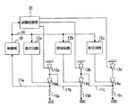
図1を参照して、本発明によるデータバス回路の構成を説明する。このデータバス回路は、制御部10、n個(この例では3個)の部位回路12a、12b、12c、電源VDDと接地間に直列接続される1対の出力バッファ13a〜13c、14a〜14c及び負荷抵抗15a〜15c、制御部10から各部位回路12a〜12cの入力側に接続される制御信号バス16及び各後段の出力バッファ14c、14b、14aから前段の出力バッファ14b、14aの入力側又は制御部10の入力端に順次接続されるデータバス17c、17b、17a及び制御部10の出力側に接続された試験回路部20より構成される。
【0020】
制御部10は、各部位回路12a〜12cに指令を送り、情報を収集し、その情報により対応する部位回路12a〜12cを制御する。各部位回路12a〜12cは、制御部10から出力される指令又は制御信号で制御され、対応する応答信号を出力バッファ14a〜14cに出力する。出力バッファ14a〜14cは、各部位回路12a〜12cからの応答信号をデータバス17a〜17cに載せる。試験回路部20は、出力バッファ14a〜14cに直列接続される試験用出力バッファ13a〜13cに試験信号を送る。また、試験用出力バッファ13a〜13cは、試験回路部20から送られてくる試験信号を受け、各出力バッファ14a〜14cの入力側である前段データバス17b、17cに接続される。
【0021】
各データバス17a〜17cは、負荷抵抗又はHレベル保証の為の電源VDDにプルアップ抵抗15a〜15cを介して接続されている。
【0022】
このデータバス回路にあっては、回路が正常で故障等がない場合、制御部10から出力された制御信号は、各部位回路12a〜12c及び試験回路部20に入力される。制御部10が回答を要求している部位回路のみから制御信号を取込む。その部位回路12は、その要求に対する処理を行い、応答信号を出力バッファ14a〜14cの出力制御入力に送る。そこで、出力バッファ14a〜14cは、部位回路12a〜12cから応答信号を受け、その制御により出力のオン/オフを行う。出力バッファ14の入力端子には、前段のデータバス17が入力されている。即ち、出力バッファ14aにはデータバス17bが、出力バッファ14bには、データバス17cが接続されている。応答を要求されている部位回路12以外の出力バッファが全てオン状態の為に、応答する出力バッファ14の入力端子はLレベルとなっている。
【0023】
また、試験用出力バッファ13は、試験回路部20からの試験信号により、最終段のバッファ13以外は全てオフとなっており、高インピーダンスになっている。最終段の試験用出力バッファ13cは、通常オンでありLレベルを出力している。よって、実際に応答が必要な部位回路12に接続されている出力バッファ14は、部位回路12の応答信号の制御によって、オンの場合はLレベルを、またオフの場合はHレベルを対応するデータバス17に出力する。この信号は、制御端子がオンとなっている次段の出力バッファ14を通り、最終的にデータバス17aに伝わり、制御部10に入力される。この信号が、制御部10で対象となった部位回路12の応答信号と認識され、正常に処理されたと判断されることとなる。
【0024】
次に、このデータバス回路内に故障が発生した場合につき説明する。この場合には制御部10に正常な応答が戻って来ない。制御部10からの制御信号によって、各部位回路12の個別試験が開始される。
【0025】
先ず、対象になる部位回路(例えば12b)が決められる。それ以前の各部位回路(例えば12a)には、対応する出力バッファ14の制御端子をオフとし出力を高インピーダンスする。またそれ以後の各部位回路(例えば12c)には、対応する出力バッファ14の制御端子をオンとし、出力をスルーにする。次に、対象となる部位回路12aの試験用出力バッファ13を試験回路部20からの試験信号で出力制御端子をオンとさせる。これにより、その出力をLレベルとする。これで対象となる部位回路12が完全に制御部10と1対1となり、外部の影響を受けず自由に回路の正常性と回線の状態を確認可能になる。ここで、制御部10への応答が正常であれば、対象となった部位回路(例えば12b)及びそれ以降のデータバス17と出力バッファ14は正常と判断される。よって故障は、この対象部位回路12以外となる。
【0026】
もし、この状態で、制御部10への応答が異常であれば、対象の部位回路(12b)又はそれ以降の出力バッファ14の異常か、1段前の出力バッファ14の異常となり、障害箇所のしぼり込みができる。更に対象部位回路12を前後にずらすことにより、障害箇所の一層のしぼり込みができる。
【0027】
次に、図1のデータバス回路の動作タイミングチャートを示す図2につき簡単に説明する。このデータバス回路の動作は上述のとおりであるので、(a)乃至(j)のタイミングチャートにつき説明する。
【0028】
(a)は、制御部10から各部位回路12a〜12cに送られる制御信号4−1である。
(b)は、部位回路12が取込む制御信号4−2である。
(c)は、部位回路12からの応答信号4−3である。
(d)は、出力バッファ14からデータバス17に出力されるデータバス信号4−4である。
(e)は、回路故障又はデータバス障害の場合のデータバス信号4−5である。
(f)は、部位回路12からの応答信号が正常な場合の正常信号4−6である。
(g)は、部位回路12からの応答信号が異常である異常信号4−7である。
(h)は、各部位回路12からの各応答信号が正常な場合の信号4−8である。
(i)は、各部位回路12からの各応答信号が異常な場合の信号4−9である。
(j)は、部位回路12からの応答信号が異常な場合のデータバス17の信号4−10である。
【0029】
以上説明した如く本発明によるデータバス回路は、制御部、複数の部位回路、出力バッファ、試験用出力バッファ及び試験回路部を設けることにより、監視機能付きデータバス回路が得られる。しかし、本発明は斯る特定例のみに限定されるべきではなく、本発明の要旨を逸脱することなく種々の変形変更が可能である。例えば、データバス回路に含まれる部位回路の個数は用途に応じて任意数に選定することが可能である。
【0030】
【発明の効果】
上述の説明から理解される如く、本発明のデータバス回路によると、各部位回路又は部位回路間の動作監視が可能な試験回路部を設けることにより装置全体の動作が保証でき、その保守及び運用が向上する。
【図面の簡単な説明】
【図1】本発明によるデータバス回路の好適実施形態例の構成図である。
【図2】図1のデータバス回路の動作タイミングチャートである。
【図3】従来のデータバス回路の構成図である。
【図4】図4のデータバス回路の動作タイミングチャートである。
【符号の説明】
10 制御部
12a〜12c 部位回路
13a〜13c 試験用出力バッファ
14a〜14c 出力バッファ
16 制御信号バス
17a〜17c データバス
20 試験回路部[0001]
BACKGROUND OF THE INVENTION
The present invention relates to a data bus circuit, and more particularly to a data bus circuit that is used in a control processing unit of a digital processing apparatus and collects information.
[0002]
[Prior art]
In digital processing apparatuses such as computers, a plurality of devices such as processors and various memories are used. Data transmission / reception is performed between these devices, but it is not always necessary to connect them. Therefore, it is common to provide a signal transmission path composed of one or more conductors called a data bus, and to connect to the data bus when necessary to transmit and receive data between devices. This simplifies the configuration. Alternatively, an output signal is selectively output to the common data bus.
[0003]
A conventional data bus circuit used in a control system processing unit of a digital processing apparatus generally has a data reception signal bus connected from the control unit directly to the output of each part circuit of a number of part circuits in the system. It is connected. Signals are transmitted and received by controlling the output of each part circuit so that the output signals do not overlap. With such a configuration, the number of signal lines between the control unit and the plurality of partial circuits is significantly reduced, and the circuit scale is also reduced, thereby making it possible to reduce the size.
[0004]
FIG. 3 shows an example of a conventional data bus circuit. FIG. 4 shows an operation timing chart of the data bus circuit of FIG.
[0005]
In the conventional system shown in FIG. 3, the system is composed of one
[0006]
Next, the operation of the conventional system of FIG. 3 will be described with reference to the timing chart of FIG. First, the
[0007]
The output buffer 3 places the response signals 2-2 and 2-4 on the
[0008]
[Problems to be solved by the invention]
As described above, in the prior art, a large number of
[0009]
This is because the configuration of the data bus circuit can only monitor abnormality of data being communicated. Although an abnormality or circuit failure and communication abnormality in each part circuit can be determined, it has occurred in a situation where it is impossible to determine which part circuit affects the failure or communication abnormality on the data bus circuit. The identification of such a failure location is considered to be one of very important functions in recent digital processing devices and data transmission devices, and has a great influence on the identification or recovery of the failure location of the device.
[0010]
An object of the present invention is to provide a data bus circuit that has a function of facilitating maintenance or maintenance (maintenance) of a device by enabling specification of a failure location in the event of a circuit failure or line abnormality.
[0011]
[Means for Solving the Problems]
In order to solve the above-described problems, the data bus circuit according to the present invention employs the following characteristic configuration.
[0012]
(1) A data bus that includes a control unit and a plurality of part circuits that receive a control signal from the control part and output a corresponding output signal, and inputs the output of the part circuit to the control unit via a data bus In the circuit
Providing a plurality of output buffers in which the output of the part circuit is input to an output control terminal;
The data bus is a data bus circuit configured by sequentially connecting the output of the output buffer to which the output of the subsequent partial circuit among the plurality of partial circuits is connected to the input terminal of the preceding output buffer.
[0013]
(2) The data bus circuit according to (1), wherein the control signal of the control unit is input to the plurality of part circuits via a common control line.
[0014]
(3) The data bus circuit according to (1), further including a test circuit unit that receives a control signal from the control unit and inputs a failure location determination test signal to the output buffer.
[0015]
(4) The data bus circuit according to (3), wherein the test signal of the test circuit unit is input to the output control terminal of the test output buffer connected in series with the output buffer and having an output control terminal.
[0016]
(5) The data bus circuit according to (1), (2), (3) or (4) used in the control system processing unit of the digital processing device.
[0017]
DETAILED DESCRIPTION OF THE INVENTION
Hereinafter, the configuration and operation of a preferred embodiment of the data bus circuit according to the present invention will be described in detail with reference to FIG. 1 and FIG.
[0018]
FIG. 1 is a block diagram of a preferred embodiment of a data bus circuit according to the present invention. FIG. 2 is a timing chart for explaining the operation of each part of the data bus circuit of FIG.
[0019]
The configuration of the data bus circuit according to the present invention will be described with reference to FIG. This data bus circuit includes a
[0020]
The
[0021]
Each of the
[0022]
In this data bus circuit, when the circuit is normal and there is no failure or the like, the control signal output from the
[0023]
In addition, the test output buffer 13 is turned off by the test signal from the
[0024]
Next, a case where a failure occurs in the data bus circuit will be described. In this case, a normal response does not return to the
[0025]
First, a target part circuit (for example, 12b) is determined. For each part circuit (for example, 12a) before that, the control terminal of the corresponding output buffer 14 is turned off to make the output high impedance. In each subsequent circuit (for example, 12c), the control terminal of the corresponding output buffer 14 is turned on, and the output is set to through. Next, the output control terminal of the test output buffer 13 of the
[0026]
If the response to the
[0027]
Next, FIG. 2 showing an operation timing chart of the data bus circuit of FIG. 1 will be briefly described. Since the operation of the data bus circuit is as described above, the timing charts (a) to (j) will be described.
[0028]
(A) is a control signal 4-1 sent from the
(B) is a control signal 4-2 taken by the part circuit 12.
(C) is a response signal 4-3 from the part circuit 12.
(D) is a data bus signal 4-4 output from the output buffer 14 to the data bus 17.
(E) is a data bus signal 4-5 in the case of a circuit failure or a data bus failure.
(F) is a normal signal 4-6 when the response signal from the part circuit 12 is normal.
(G) is an abnormal signal 4-7 in which the response signal from the part circuit 12 is abnormal.
(H) is a signal 4-8 when each response signal from each part circuit 12 is normal.
(I) is a signal 4-9 when each response signal from each part circuit 12 is abnormal.
(J) is a signal 4-10 of the data bus 17 when the response signal from the part circuit 12 is abnormal.
[0029]
As described above, the data bus circuit according to the present invention provides a data bus circuit with a monitoring function by providing a control unit, a plurality of part circuits, an output buffer, a test output buffer, and a test circuit unit. However, the present invention should not be limited to such specific examples, and various modifications and changes can be made without departing from the gist of the present invention. For example, the number of partial circuits included in the data bus circuit can be selected as an arbitrary number according to the application.
[0030]
【The invention's effect】
As can be understood from the above description, according to the data bus circuit of the present invention, the operation of the entire apparatus can be ensured by providing a test circuit unit capable of monitoring the operation of each part circuit or between part circuits. Will improve.
[Brief description of the drawings]
FIG. 1 is a block diagram of a preferred embodiment of a data bus circuit according to the present invention.
FIG. 2 is an operation timing chart of the data bus circuit of FIG.
FIG. 3 is a configuration diagram of a conventional data bus circuit.
4 is an operation timing chart of the data bus circuit of FIG. 4;
[Explanation of symbols]
DESCRIPTION OF
Claims (5)
前記部位回路の出力が出力制御端子に入力される複数の出力バッファを設け、
前記データバスは、前記複数の部位回路のうち後段の部位回路の出力が接続されている前記出力バッファの出力を順次前段の出力バッファの入力端子に接続して構成することを特徴とするデータバス回路。In a data bus circuit that includes a control unit and a plurality of part circuits that receive a control signal from the control unit and output a corresponding output signal, and that inputs the output of the part circuit to the control unit via a data bus,
Providing a plurality of output buffers in which the output of the part circuit is input to an output control terminal;
The data bus is configured by sequentially connecting the output of the output buffer to which the output of the subsequent stage circuit among the plurality of partial circuits is connected to the input terminal of the output buffer of the previous stage. circuit.
Priority Applications (1)
| Application Number | Priority Date | Filing Date | Title |
|---|---|---|---|
| JP07941599A JP3710114B2 (en) | 1999-03-24 | 1999-03-24 | Data bus circuit |
Applications Claiming Priority (1)
| Application Number | Priority Date | Filing Date | Title |
|---|---|---|---|
| JP07941599A JP3710114B2 (en) | 1999-03-24 | 1999-03-24 | Data bus circuit |
Publications (2)
| Publication Number | Publication Date |
|---|---|
| JP2000278291A JP2000278291A (en) | 2000-10-06 |
| JP3710114B2 true JP3710114B2 (en) | 2005-10-26 |
Family
ID=13689249
Family Applications (1)
| Application Number | Title | Priority Date | Filing Date |
|---|---|---|---|
| JP07941599A Expired - Fee Related JP3710114B2 (en) | 1999-03-24 | 1999-03-24 | Data bus circuit |
Country Status (1)
| Country | Link |
|---|---|
| JP (1) | JP3710114B2 (en) |
-
1999
- 1999-03-24 JP JP07941599A patent/JP3710114B2/en not_active Expired - Fee Related
Also Published As
| Publication number | Publication date |
|---|---|
| JP2000278291A (en) | 2000-10-06 |
Similar Documents
| Publication | Publication Date | Title |
|---|---|---|
| CN109101009B (en) | Fault diagnosis system and server | |
| US4429362A (en) | Data buffer operating in response to computer halt signal | |
| JP3710114B2 (en) | Data bus circuit | |
| JP2687776B2 (en) | Package identification number setting method | |
| KR930006862B1 (en) | Triple modular redundency method | |
| KR930006863B1 (en) | Supervising circuit for a receiving bus | |
| JP2583767B2 (en) | Gaming machine system | |
| JP2692739B2 (en) | Gaming machine system | |
| KR950007438B1 (en) | Repeater of packet bus device for electronic exchanger | |
| JP3678265B2 (en) | Crossbar switch device and diagnostic method thereof | |
| JPH10154971A (en) | Multiplex communication equipment | |
| JP2548063Y2 (en) | Multi-distributor | |
| JP2749417B2 (en) | Priority control circuit | |
| JPS58129859A (en) | Transmitting method of process signal | |
| JP2000347706A (en) | Plant controller | |
| JPH0644165B2 (en) | Electronic copier control device | |
| JPH0126215B2 (en) | ||
| JPH01296828A (en) | Condition signal transmitting system | |
| JPS63182761A (en) | Bus diagnozing system | |
| JP2001051912A (en) | Serial data transfer system and abnormality detecting method | |
| JPH05250224A (en) | Monitoring control system | |
| JPH03246735A (en) | Monitoring signal detecting system | |
| JPS62293453A (en) | Multiple bus system data processor | |
| JPS63240660A (en) | Composite computer system | |
| JPS60105014A (en) | Signal input device of monitor device |
Legal Events
| Date | Code | Title | Description |
|---|---|---|---|
| A977 | Report on retrieval |
Free format text: JAPANESE INTERMEDIATE CODE: A971007 Effective date: 20050708 |
|
| TRDD | Decision of grant or rejection written | ||
| A01 | Written decision to grant a patent or to grant a registration (utility model) |
Free format text: JAPANESE INTERMEDIATE CODE: A01 Effective date: 20050713 |
|
| A61 | First payment of annual fees (during grant procedure) |
Free format text: JAPANESE INTERMEDIATE CODE: A61 Effective date: 20050808 |
|
| R150 | Certificate of patent or registration of utility model |
Free format text: JAPANESE INTERMEDIATE CODE: R150 |
|
| FPAY | Renewal fee payment (event date is renewal date of database) |
Free format text: PAYMENT UNTIL: 20080819 Year of fee payment: 3 |
|
| S531 | Written request for registration of change of domicile |
Free format text: JAPANESE INTERMEDIATE CODE: R313531 |
|
| FPAY | Renewal fee payment (event date is renewal date of database) |
Free format text: PAYMENT UNTIL: 20080819 Year of fee payment: 3 |
|
| R350 | Written notification of registration of transfer |
Free format text: JAPANESE INTERMEDIATE CODE: R350 |
|
| LAPS | Cancellation because of no payment of annual fees |