JP3702152B2 - Semiconductor device - Google Patents
Semiconductor device Download PDFInfo
- Publication number
- JP3702152B2 JP3702152B2 JP2000196426A JP2000196426A JP3702152B2 JP 3702152 B2 JP3702152 B2 JP 3702152B2 JP 2000196426 A JP2000196426 A JP 2000196426A JP 2000196426 A JP2000196426 A JP 2000196426A JP 3702152 B2 JP3702152 B2 JP 3702152B2
- Authority
- JP
- Japan
- Prior art keywords
- lead
- bonding
- semiconductor chip
- chip
- bridge
- Prior art date
- Legal status (The legal status is an assumption and is not a legal conclusion. Google has not performed a legal analysis and makes no representation as to the accuracy of the status listed.)
- Expired - Fee Related
Links
Images


Classifications
-
- H—ELECTRICITY
- H01—ELECTRIC ELEMENTS
- H01L—SEMICONDUCTOR DEVICES NOT COVERED BY CLASS H10
- H01L24/00—Arrangements for connecting or disconnecting semiconductor or solid-state bodies; Methods or apparatus related thereto
- H01L24/01—Means for bonding being attached to, or being formed on, the surface to be connected, e.g. chip-to-package, die-attach, "first-level" interconnects; Manufacturing methods related thereto
- H01L24/42—Wire connectors; Manufacturing methods related thereto
- H01L24/47—Structure, shape, material or disposition of the wire connectors after the connecting process
- H01L24/49—Structure, shape, material or disposition of the wire connectors after the connecting process of a plurality of wire connectors
-
- H—ELECTRICITY
- H01—ELECTRIC ELEMENTS
- H01L—SEMICONDUCTOR DEVICES NOT COVERED BY CLASS H10
- H01L2224/00—Indexing scheme for arrangements for connecting or disconnecting semiconductor or solid-state bodies and methods related thereto as covered by H01L24/00
- H01L2224/01—Means for bonding being attached to, or being formed on, the surface to be connected, e.g. chip-to-package, die-attach, "first-level" interconnects; Manufacturing methods related thereto
- H01L2224/02—Bonding areas; Manufacturing methods related thereto
- H01L2224/04—Structure, shape, material or disposition of the bonding areas prior to the connecting process
- H01L2224/05—Structure, shape, material or disposition of the bonding areas prior to the connecting process of an individual bonding area
- H01L2224/0554—External layer
- H01L2224/0555—Shape
- H01L2224/05552—Shape in top view
- H01L2224/05554—Shape in top view being square
-
- H—ELECTRICITY
- H01—ELECTRIC ELEMENTS
- H01L—SEMICONDUCTOR DEVICES NOT COVERED BY CLASS H10
- H01L2224/00—Indexing scheme for arrangements for connecting or disconnecting semiconductor or solid-state bodies and methods related thereto as covered by H01L24/00
- H01L2224/01—Means for bonding being attached to, or being formed on, the surface to be connected, e.g. chip-to-package, die-attach, "first-level" interconnects; Manufacturing methods related thereto
- H01L2224/42—Wire connectors; Manufacturing methods related thereto
- H01L2224/44—Structure, shape, material or disposition of the wire connectors prior to the connecting process
- H01L2224/45—Structure, shape, material or disposition of the wire connectors prior to the connecting process of an individual wire connector
- H01L2224/45001—Core members of the connector
- H01L2224/45099—Material
- H01L2224/451—Material with a principal constituent of the material being a metal or a metalloid, e.g. boron (B), silicon (Si), germanium (Ge), arsenic (As), antimony (Sb), tellurium (Te) and polonium (Po), and alloys thereof
- H01L2224/45138—Material with a principal constituent of the material being a metal or a metalloid, e.g. boron (B), silicon (Si), germanium (Ge), arsenic (As), antimony (Sb), tellurium (Te) and polonium (Po), and alloys thereof the principal constituent melting at a temperature of greater than or equal to 950°C and less than 1550°C
- H01L2224/45144—Gold (Au) as principal constituent
-
- H—ELECTRICITY
- H01—ELECTRIC ELEMENTS
- H01L—SEMICONDUCTOR DEVICES NOT COVERED BY CLASS H10
- H01L2224/00—Indexing scheme for arrangements for connecting or disconnecting semiconductor or solid-state bodies and methods related thereto as covered by H01L24/00
- H01L2224/01—Means for bonding being attached to, or being formed on, the surface to be connected, e.g. chip-to-package, die-attach, "first-level" interconnects; Manufacturing methods related thereto
- H01L2224/42—Wire connectors; Manufacturing methods related thereto
- H01L2224/47—Structure, shape, material or disposition of the wire connectors after the connecting process
- H01L2224/48—Structure, shape, material or disposition of the wire connectors after the connecting process of an individual wire connector
- H01L2224/4805—Shape
- H01L2224/4809—Loop shape
- H01L2224/48091—Arched
-
- H—ELECTRICITY
- H01—ELECTRIC ELEMENTS
- H01L—SEMICONDUCTOR DEVICES NOT COVERED BY CLASS H10
- H01L2224/00—Indexing scheme for arrangements for connecting or disconnecting semiconductor or solid-state bodies and methods related thereto as covered by H01L24/00
- H01L2224/01—Means for bonding being attached to, or being formed on, the surface to be connected, e.g. chip-to-package, die-attach, "first-level" interconnects; Manufacturing methods related thereto
- H01L2224/42—Wire connectors; Manufacturing methods related thereto
- H01L2224/47—Structure, shape, material or disposition of the wire connectors after the connecting process
- H01L2224/48—Structure, shape, material or disposition of the wire connectors after the connecting process of an individual wire connector
- H01L2224/481—Disposition
- H01L2224/48135—Connecting between different semiconductor or solid-state bodies, i.e. chip-to-chip
- H01L2224/48137—Connecting between different semiconductor or solid-state bodies, i.e. chip-to-chip the bodies being arranged next to each other, e.g. on a common substrate
-
- H—ELECTRICITY
- H01—ELECTRIC ELEMENTS
- H01L—SEMICONDUCTOR DEVICES NOT COVERED BY CLASS H10
- H01L2224/00—Indexing scheme for arrangements for connecting or disconnecting semiconductor or solid-state bodies and methods related thereto as covered by H01L24/00
- H01L2224/01—Means for bonding being attached to, or being formed on, the surface to be connected, e.g. chip-to-package, die-attach, "first-level" interconnects; Manufacturing methods related thereto
- H01L2224/42—Wire connectors; Manufacturing methods related thereto
- H01L2224/47—Structure, shape, material or disposition of the wire connectors after the connecting process
- H01L2224/48—Structure, shape, material or disposition of the wire connectors after the connecting process of an individual wire connector
- H01L2224/481—Disposition
- H01L2224/48151—Connecting between a semiconductor or solid-state body and an item not being a semiconductor or solid-state body, e.g. chip-to-substrate, chip-to-passive
- H01L2224/48221—Connecting between a semiconductor or solid-state body and an item not being a semiconductor or solid-state body, e.g. chip-to-substrate, chip-to-passive the body and the item being stacked
- H01L2224/48245—Connecting between a semiconductor or solid-state body and an item not being a semiconductor or solid-state body, e.g. chip-to-substrate, chip-to-passive the body and the item being stacked the item being metallic
- H01L2224/48247—Connecting between a semiconductor or solid-state body and an item not being a semiconductor or solid-state body, e.g. chip-to-substrate, chip-to-passive the body and the item being stacked the item being metallic connecting the wire to a bond pad of the item
-
- H—ELECTRICITY
- H01—ELECTRIC ELEMENTS
- H01L—SEMICONDUCTOR DEVICES NOT COVERED BY CLASS H10
- H01L2224/00—Indexing scheme for arrangements for connecting or disconnecting semiconductor or solid-state bodies and methods related thereto as covered by H01L24/00
- H01L2224/01—Means for bonding being attached to, or being formed on, the surface to be connected, e.g. chip-to-package, die-attach, "first-level" interconnects; Manufacturing methods related thereto
- H01L2224/42—Wire connectors; Manufacturing methods related thereto
- H01L2224/47—Structure, shape, material or disposition of the wire connectors after the connecting process
- H01L2224/49—Structure, shape, material or disposition of the wire connectors after the connecting process of a plurality of wire connectors
- H01L2224/491—Disposition
- H01L2224/4912—Layout
- H01L2224/49171—Fan-out arrangements
-
- H—ELECTRICITY
- H01—ELECTRIC ELEMENTS
- H01L—SEMICONDUCTOR DEVICES NOT COVERED BY CLASS H10
- H01L2224/00—Indexing scheme for arrangements for connecting or disconnecting semiconductor or solid-state bodies and methods related thereto as covered by H01L24/00
- H01L2224/80—Methods for connecting semiconductor or other solid state bodies using means for bonding being attached to, or being formed on, the surface to be connected
- H01L2224/85—Methods for connecting semiconductor or other solid state bodies using means for bonding being attached to, or being formed on, the surface to be connected using a wire connector
- H01L2224/8512—Aligning
- H01L2224/85148—Aligning involving movement of a part of the bonding apparatus
-
- H—ELECTRICITY
- H01—ELECTRIC ELEMENTS
- H01L—SEMICONDUCTOR DEVICES NOT COVERED BY CLASS H10
- H01L2924/00—Indexing scheme for arrangements or methods for connecting or disconnecting semiconductor or solid-state bodies as covered by H01L24/00
- H01L2924/01—Chemical elements
- H01L2924/01004—Beryllium [Be]
-
- H—ELECTRICITY
- H01—ELECTRIC ELEMENTS
- H01L—SEMICONDUCTOR DEVICES NOT COVERED BY CLASS H10
- H01L2924/00—Indexing scheme for arrangements or methods for connecting or disconnecting semiconductor or solid-state bodies as covered by H01L24/00
- H01L2924/01—Chemical elements
- H01L2924/01006—Carbon [C]
-
- H—ELECTRICITY
- H01—ELECTRIC ELEMENTS
- H01L—SEMICONDUCTOR DEVICES NOT COVERED BY CLASS H10
- H01L2924/00—Indexing scheme for arrangements or methods for connecting or disconnecting semiconductor or solid-state bodies as covered by H01L24/00
- H01L2924/01—Chemical elements
- H01L2924/01014—Silicon [Si]
-
- H—ELECTRICITY
- H01—ELECTRIC ELEMENTS
- H01L—SEMICONDUCTOR DEVICES NOT COVERED BY CLASS H10
- H01L2924/00—Indexing scheme for arrangements or methods for connecting or disconnecting semiconductor or solid-state bodies as covered by H01L24/00
- H01L2924/01—Chemical elements
- H01L2924/01033—Arsenic [As]
-
- H—ELECTRICITY
- H01—ELECTRIC ELEMENTS
- H01L—SEMICONDUCTOR DEVICES NOT COVERED BY CLASS H10
- H01L2924/00—Indexing scheme for arrangements or methods for connecting or disconnecting semiconductor or solid-state bodies as covered by H01L24/00
- H01L2924/01—Chemical elements
- H01L2924/01047—Silver [Ag]
-
- H—ELECTRICITY
- H01—ELECTRIC ELEMENTS
- H01L—SEMICONDUCTOR DEVICES NOT COVERED BY CLASS H10
- H01L2924/00—Indexing scheme for arrangements or methods for connecting or disconnecting semiconductor or solid-state bodies as covered by H01L24/00
- H01L2924/01—Chemical elements
- H01L2924/01079—Gold [Au]
-
- H—ELECTRICITY
- H01—ELECTRIC ELEMENTS
- H01L—SEMICONDUCTOR DEVICES NOT COVERED BY CLASS H10
- H01L2924/00—Indexing scheme for arrangements or methods for connecting or disconnecting semiconductor or solid-state bodies as covered by H01L24/00
- H01L2924/01—Chemical elements
- H01L2924/01082—Lead [Pb]
-
- H—ELECTRICITY
- H01—ELECTRIC ELEMENTS
- H01L—SEMICONDUCTOR DEVICES NOT COVERED BY CLASS H10
- H01L2924/00—Indexing scheme for arrangements or methods for connecting or disconnecting semiconductor or solid-state bodies as covered by H01L24/00
- H01L2924/013—Alloys
- H01L2924/014—Solder alloys
-
- H—ELECTRICITY
- H01—ELECTRIC ELEMENTS
- H01L—SEMICONDUCTOR DEVICES NOT COVERED BY CLASS H10
- H01L2924/00—Indexing scheme for arrangements or methods for connecting or disconnecting semiconductor or solid-state bodies as covered by H01L24/00
- H01L2924/06—Polymers
- H01L2924/078—Adhesive characteristics other than chemical
- H01L2924/07802—Adhesive characteristics other than chemical not being an ohmic electrical conductor
-
- H—ELECTRICITY
- H01—ELECTRIC ELEMENTS
- H01L—SEMICONDUCTOR DEVICES NOT COVERED BY CLASS H10
- H01L2924/00—Indexing scheme for arrangements or methods for connecting or disconnecting semiconductor or solid-state bodies as covered by H01L24/00
- H01L2924/30—Technical effects
- H01L2924/301—Electrical effects
- H01L2924/3011—Impedance
Description
【0001】
【発明の属する技術分野】
本発明は、複数の半導体チップがアイランドに平面的におよび一部は立体的に配列された半導体装置に関する。
【0002】
【従来の技術】
近年、モールド型半導体チップが高機能に成っており、複数の半導体チップを1パッケージ化するものが開発されている。
【0003】
この技術として例えば、特開平5−121645号公報の従来例がある。これは、図5に示すように、第1の半導体チップ1および第2の半導体チップ2が1つのリードフレームの1つのアイランド3に固着されている。第1および第2の半導体チップ1、2のボンディングパット4、5とリード6の先端が金属細線7により実現され、全体が樹脂で封止されている。そして、第1の半導体チップ1と第2の半導体チップ2との間の接続は、ボンディングパット8、9の間を金属細線10により接続されている。
【0004】
【発明が解決しようとする課題】
金属細線による電気的接続は、一般にワイヤボンディングにより実現され、一端はボールボンディング、他端はステッチボンディングにより実現されている。また、ステッチボンディングは、金属細線をキャピラリーチップ(ボンディングツール)で強く押さえ力で引きちぎるため、ステッチボンディング下の部分には直接キャピラリーチップがぶつかりストレスが加わる。リード6とボンディングパット5との間は、リード側をステッチボンディング、ボンディングパット側をボールボンディングにすれば、半導体チップにはストレスは加わりにくいが、ボンディングパット8とボンディングパット9との間は、どちらか一方は、必ずステッチボンディングとなり、どちらか一方の半導体チップのボンディングパットにストレスが加わる。最近は、ボンディングパットの下に保護ダイオード等の半導体装置が組み込まれるため、このストレスにより半導体装置自身が不良になったり、ボンディングパット下の半導体素子が破壊してしまう問題があった。
【0005】
【課題を解決するための手段】
本発明は、前述の課題に鑑みてなされ、第1に、第1のアイランドと第2のアイランド間を橋渡しする2本の橋絡リードと、前記第1のアイランド、前記第2のアイランドおよび橋絡リードとで囲まれた領域に設けられ、電気的に分離されたボンディング可能なブリッヂを設けることで、半導体チップ側の接続はボールボンディングで、前記ブリッヂ側の接続はステッチボンディングで実現することができる。また、前記2本の橋絡リードはそれぞれプレス・カット等で第1のアイランドと第2のアイランドを電気的に分離し、第1の半導体チップのノイズが第2の半導体チップへ侵入しないような構造をとっている。
【0006】
また、前記ブリッヂを接着テープにより固定し、この接着テープが設けられた領域に対応する橋絡リードに前記切断分離を設けることで、この切断分離部とブリッヂの安定化を図っている。
【0007】
また、前記第1の半導体チップおよび前記第2の半導体チップを、絶縁性接着剤により固着することで解決するものである。この接着剤(例えば体積抵抗率10の5乗程度)の使用で、チップとアイランド間のインピーダンスが高くなり、ノイズの伝搬を抑制することができる。
【0008】
【発明の実施の形態】
以下に本発明の第1の実施の形態を図1を参照しながら詳細に説明する。
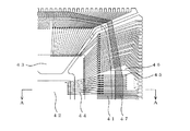
【0009】
図に示したように、第1のアイランド20上には第1の親子半導体チップ22が形成され、第2のアイランド21上には第2の半導体チップ24が形成されている。第1および第2の半導体チップ22、24のシリコン表面には、前工程において各種の能動、受動回路素子が形成され、更にチップの周辺部に外部接続用のボンディングパット25、26、27が形成されている。そのボンディングパット25、26、27を被覆するようにシリコン窒化膜、シリコン酸化膜、ポリイミド系絶縁膜などのパッシベーション被膜が形成され、ボンディングパット25、26、27の上部は、ボンディング接続のために開口されている。
【0010】
第1および第2の半導体チップ22、24はリードフレームの第1および第2のアイランド20、21に接着材(ここでは、半田や銀ベースト等)によりダイボンドされ、第1および第2の半導体チップ22、24表面のボンディングパット25、26、27には、金線等のボンディングワイヤ28の一端がボールボンディングでワイヤボンドされており、ボンディングワイヤ28の他端は外部導出用のリード29の先端部にステッチボンディングでワイヤボンドされている。
【0011】
一方、第1の半導体チップ22と第2の半導体チップ24との接続は、以下の構成になっている。まず、第1および第2の半導体チップ22、24との間に対応する第1および第2のアイランド20、21には、開口部30が設けられ、この中には、必要な本数だけアイランド状のブリッヂ31が設けられている。
【0012】
前文では、第1および第2のアイランド20、21に開口部30を設けたと述べたが、第1のアイランド20と第2のアイランド21とが2本の橋絡リード32、33で囲まれた領域が、前記開口部30を構成しているとも言える。また、後述するがそれぞれの橋絡リード32、33には離間部34が設けられている。
【0013】
本実施例では、リードフレーム形成時(プレスカットやエッチング)、第1および第2のアイランド20、21と一体のブリッヂ31、第1および第2のアイランド20、21と一体の橋絡リード32、33(ただし橋絡部に離間部34が形成される)を形成しておき、図1のように接着テープ35を貼った後に、ブリッヂ31を第1および第2のアイランド20、21から切り離せばよい。接着テープ35は、ブリッヂ31と離間部34を構成する橋絡リード32、33を貼りつけることになる。
【0014】
本発明は、このブリッヂ31とボンディングパット25、26、27との接続について、第1および第2の半導体チップ22、24側のボンディングパット25、26、27をボールボンディングで行い、ブリッヂ31側をステッチボンディングで行うことに特徴を有する。
【0015】
また必要により、第1の半導体チップ22と第2の半導体チップ24に組み込まれる回路により、相互干渉を生じる場合がある。例えば、第1の半導体チップ22から発生するノイズが第1のアイランド20、橋絡リード32、33、第2のアイランド21を介して第2の半導体チップ24に侵入する場合は、ここにプレスカット等で離間部34を設けることで、このノイズの侵入を防止できる。
【0016】
金属細線によるワイヤボンディングは、一端はボールボンディング、他端はステッチボンディンにより実現されている。特に、ステッチボンディングは、金属細線をキャピラリーチップで強く押さえ、力で引きちぎるため、ステッチボンディング下の部分にはストレスが加わるが、ブリッヂ31側をステッチボンディングとし第1および第2の半導体チップ22、24側をボールボンディングとしたため、この第1および第2の半導体チップ22、24のボンディングパット25、26、27下に加わるストレスを抑制することができる。従って、ボンディングパット25、26、27下の半導体素子の劣化を抑制することができる。
【0017】
第1および第2の半導体チップ22、24、第1および第2のアイランド20、21の近傍まで延在される複数のリード23、29の先端部、およびボンディングワイヤ28を含む主要部は、一点鎖線の如くエポキシ系の熱硬化樹脂36でモールドされ、パッケージ化される。
【0018】
このような半導体装置の構造はフラッシュメモリ等に用いられ、半導体チップを2段に搭載することで高集積化ができ、また、メモリー容量を倍にすることができる。
【0019】
次に、第2の実施の形態について図2から図4を参照して説明する。図2は図1に示した半導体装置と同様に親子チップを搭載する半導体チップの平面図である。また、図2の半導体装置のA−A線断面図である図3に示したように、この半導体装置は、アイランド上にマザーチップ43を、そして、マザーチップ43上にドウターチップ42をそれぞれ接着テープ48または半田や銀ペースト等を用いて接着されている。そして、マザーチップ43およびドウターチップ42にボールボンディングされたボンディングワイヤ44、49は、互いに接触しショートしないように、ボンディングワイヤ49は、M型に加工されて第2のリード45にステッチボンディングされている。尚、ボンディングワイヤ49は必ずしもM型の形状でステッチボンディングされなくても良く、ボンディングワイヤ44、49が互いに接触しない構造であれば良い。
【0020】
そして、この半導体装置の第2のリード45は、第1の実施の形態でのブリッジ31と同様の役割を果たす。第2のリード45は、隣接する第1のリード41や電気的に使用されないリード52に接続された状態で加工される。そして、第2のリード45が接着テープ47で固定された後に、プレスカットにて第1のリード41やリード52から切り離されることで、浮きピン状に形成される。
【0021】
そのため、この第2のリード45は、接着テープ47で接着されることでフレーム上に固定される。このとき、第1および第2のリード41、45はリード幅が狭く形成されている。そのため、接着テープ47の接着面積を確保するため第2のリード45に隣接する第1のリード41に幅の広い部分46を設けている。そのことにより、接着テープ47は第1および第2のリード41、45上に確実に接着し、第2のリード45は固定される。
【0022】
その結果、第2のリード45は、マザーチップ43とドウターチップ42とを電気的に接続するとき、第2のリード45は接着テープ47で固定されているため浮き上がりや移動等を防止することができ、良好なワイヤーボンディングが可能となる。ここで、接着テープ47は、半導体チップを囲むように第1および第2のリード41、45上を全周に渡り形成される場合や、また、第2のリード45および隣接して設けられる第1のリード41の幅の広い部分46を主に利用してその部分で形成される場合もある。
【0023】
本発明は、第1の実施の形態において、このブリッヂ31とボンディングパット25、26、27との接続について、第1および第2の半導体チップ22、24側のボンディングパット25,26、27をボールボンディングで行い、ブリッヂ31側をステッチボンディングで行うことに特徴を有する。
【0024】
また、接着テープ35は前実施の形態と同様に、ブリッヂ31や離間部34を有する橋絡リード32、33を支持している。従って、離間部34により、一方の半導体チップから発生するノイズが、橋絡リード32、33を介して他方のチップへ入るのを防止することができる。
【0025】
特に、ノイズの伝搬の原因が、半導体チップを固着する接着材にあることが判った。つまり、銀入りの接着剤(銀ペースト)を採用すると、ノイズがペースト、第1および第2のアイランド20、21を介して他方のチップに伝搬することが判った。
【0026】
例えば、一方の半導体チップがILLによるデジタルオートバランス回路内蔵で、1〜8(Hz)の動作クロックを持ち、他方の半導体チップは、C−MOSロジックによるデジタルディレイライン内蔵で、数100〜数MHzの動作クロックを有した場合、ディレイラインで発生する動作クロックノイズがオートバランス回路の動作クロックに混入し、動作速度が速くなる等の異常動作が発生した。
【0027】
しかし、前記離間部34の設置またはインピーダンスの高い絶縁性接着剤によるチップの固着で、これらの問題が解決された。この絶縁性接着剤は、片方の半導体チップに採用しても良いが、プロセス上両者に採用しても良い。
【0028】
そして、第2の実施の形態において、第2のリード45のようにリードが浮きピン状に形成される場合、第2のリード45に隣接する第1のリード41に幅の広い部分46を設ける。そのことにより、第2のリード45を接着テープ47で固定するとき、接着テープ47の接着面積が確保され、第2のリード45がより安定して固定され、半導体チップとの良好なワイヤーボンディングを可能にすることができる。
【0029】
【発明の効果】
以上に説明した通り、本発明によれば、第1に、2つの半導体チップの間に位置するアイランドに開口部を設け、この開口部にブリッヂを設け、半導体チップ側の接続はボールボンディングで、前記ブリッヂ側の接続はステッチボンディングで金属細線をワイヤーボンディングすることで、ボンディングパット下の半導体素子の劣化を防止することができる。
【0030】
しかもチップとチップの接続は、1本の金属細線から2本の金属細線に分割したため、ボンディングの際にこの金属細線の高さを低くすることができる。従って、封止樹脂の厚みを薄くすることができる。
【0031】
第2に、半導体チップを2段に搭載し半導体装置を形成したことで、高集積化が可能となり、また、メモリー容量が増大された半導体装置を得ることができる。
【0032】
第3に、橋絡リードの設置または絶縁性接着剤の使用で、一方のチップから他方へのノイズの侵入を制御することができる。
【0033】
また、ブリッヂをリードフレームの形成時に同時に形成するため、ブリッヂをプレスで簡単にに分離でき、また、接着テープによりブリッヂを固定できるため、良好なワイヤーボンディングが可能となる。
【0034】
第4に、浮きピンに形成されたリードおよびそのリードに隣接するリードに幅の広いリードを形成し一体に接着テープで固定することで、浮きピン状のリードが確実に固定され半導体チップとの良好なワイヤーボンディングが可能となる。
【図面の簡単な説明】
【図1】本発明の第1の実施の形態を説明する半導体装置の平面図である。
【図2】本発明の第1および第2の実施の形態を説明する半導体装置の平面図である。
【図3】図2に示した本発明の半導体装置のA−A線断面図である。
【図4】本発明の第2の実施の形態を説明する半導体装置の平面図である。
【図5】従来の半導体装置の平面図である。[0001]
BACKGROUND OF THE INVENTION
The present invention relates to a semiconductor device in which a plurality of semiconductor chips are arranged on an island in a planar manner and partly in a three-dimensional manner.
[0002]
[Prior art]
In recent years, a mold type semiconductor chip has a high function, and a semiconductor chip in which a plurality of semiconductor chips are packaged has been developed.
[0003]
As this technique, for example, there is a conventional example of JP-A-5-121645. As shown in FIG. 5, the
[0004]
[Problems to be solved by the invention]
The electrical connection by the fine metal wire is generally realized by wire bonding, one end is realized by ball bonding and the other end is realized by stitch bonding. In stitch bonding, a fine metal wire is strongly pressed by a capillary tip (bonding tool) and is torn off with a force, so that the capillary tip directly hits the portion under the stitch bonding and stress is applied. Between the
[0005]
[Means for Solving the Problems]
The present invention has been made in view of the above-mentioned problems. First, two bridge leads that bridge between the first island and the second island, the first island, the second island, and the bridge By providing a bondable bridge that is electrically isolated and provided in a region surrounded by the wire leads, the connection on the semiconductor chip side can be realized by ball bonding, and the connection on the bridge side can be realized by stitch bonding. it can. The two bridging leads electrically separate the first island and the second island by press cutting or the like so that the noise of the first semiconductor chip does not enter the second semiconductor chip. It has a structure.
[0006]
In addition, the bridge is fixed by an adhesive tape, and the cutting and separating is provided in the bridging lead corresponding to the region where the adhesive tape is provided, thereby stabilizing the cutting and separating portion and the bridge.
[0007]
Further, the problem is solved by fixing the first semiconductor chip and the second semiconductor chip with an insulating adhesive. Use of this adhesive (for example, about the fifth power of volume resistivity 10) increases the impedance between the chip and the island, and can suppress the propagation of noise.
[0008]
DETAILED DESCRIPTION OF THE INVENTION
Hereinafter, a first embodiment of the present invention will be described in detail with reference to FIG.
[0009]
As shown in the figure, a first parent-
[0010]
The first and
[0011]
On the other hand, the connection between the
[0012]
In the preceding sentence, it was described that the opening 30 was provided in the first and
[0013]
In this embodiment, when the lead frame is formed (press cut or etching), the bridge 31 integral with the first and
[0014]
In the present invention, for the connection between the bridge 31 and the
[0015]
If necessary, mutual interference may occur due to circuits incorporated in the
[0016]
Wire bonding using fine metal wires is realized by ball bonding at one end and stitch bonding at the other end. In particular, in stitch bonding, a metal thin wire is strongly pressed by a capillary chip and is torn off by force. Therefore, stress is applied to a portion under the stitch bonding, but the first and
[0017]
The main parts including the first and
[0018]
Such a structure of a semiconductor device is used for a flash memory or the like. By mounting semiconductor chips in two stages, high integration can be achieved and the memory capacity can be doubled.
[0019]
Next, a second embodiment will be described with reference to FIGS. FIG. 2 is a plan view of a semiconductor chip on which a parent-child chip is mounted in the same manner as the semiconductor device shown in FIG. Further, as shown in FIG. 3 which is a cross-sectional view taken along line AA of the semiconductor device of FIG. 2, this semiconductor device has a mother chip 43 bonded onto the island and a daughter chip 42 bonded onto the mother chip 43. Bonding is performed using
[0020]
The second lead 45 of this semiconductor device plays the same role as the bridge 31 in the first embodiment. The second lead 45 is processed in a state where it is connected to the adjacent
[0021]
Therefore, the second lead 45 is fixed on the frame by being bonded with the
[0022]
As a result, when the second lead 45 electrically connects the mother chip 43 and the daughter chip 42, the second lead 45 is fixed by the
[0023]
According to the present invention, in the first embodiment, the
[0024]
Further, the adhesive tape 35 supports the bridging leads 32 and 33 having the bridge 31 and the separating
[0025]
In particular, it has been found that the cause of noise propagation is the adhesive that fixes the semiconductor chip. That is, it has been found that when a silver-containing adhesive (silver paste) is employed, noise propagates to the other chip via the paste and the first and
[0026]
For example, one semiconductor chip has a built-in digital autobalance circuit by ILL and has an operation clock of 1 to 8 (Hz), and the other semiconductor chip has a built-in digital delay line by C-MOS logic and has several hundred to several MHz. When the operation clock is included, the operation clock noise generated in the delay line is mixed into the operation clock of the auto balance circuit, and an abnormal operation such as an increase in the operation speed occurs.
[0027]
However, these problems have been solved by installing the spacing
[0028]
In the second embodiment, when the lead is formed like a floating pin like the second lead 45, the wide portion 46 is provided in the
[0029]
【The invention's effect】
As described above, according to the present invention, first, an opening is provided in an island located between two semiconductor chips, a bridge is provided in the opening, and the connection on the semiconductor chip side is performed by ball bonding. For the connection on the bridge side, deterioration of the semiconductor element under the bonding pad can be prevented by wire bonding the fine metal wire by stitch bonding.
[0030]
In addition, since the chip-to-chip connection is divided into two fine metal wires from one fine metal wire, the height of the fine metal wire can be lowered during bonding. Therefore, the thickness of the sealing resin can be reduced.
[0031]
Second, since the semiconductor device is formed by mounting the semiconductor chips in two stages, a high integration can be achieved and a semiconductor device with an increased memory capacity can be obtained.
[0032]
Third, the installation of bridge leads or the use of an insulating adhesive can control the intrusion of noise from one chip to the other.
[0033]
Further, since the bridge is formed at the same time as the lead frame is formed, the bridge can be easily separated with a press, and the bridge can be fixed with an adhesive tape, so that excellent wire bonding can be achieved.
[0034]
Fourthly, by forming a wide lead on the lead formed on the floating pin and the lead adjacent to the lead and fixing the lead integrally with an adhesive tape, the floating pin-shaped lead is securely fixed to the semiconductor chip. Good wire bonding is possible.
[Brief description of the drawings]
FIG. 1 is a plan view of a semiconductor device for explaining a first embodiment of the present invention;
FIG. 2 is a plan view of a semiconductor device for explaining first and second embodiments of the present invention;
3 is a cross-sectional view taken along line AA of the semiconductor device of the present invention shown in FIG. 2. FIG.
FIG. 4 is a plan view of a semiconductor device for explaining a second embodiment of the present invention;
FIG. 5 is a plan view of a conventional semiconductor device.
Claims (2)
前記第1の半導体チップ上に設けられた第2の半導体チップと、
前記アイランドの周辺に設けられた複数の第1のリードと、
前記アイランドの周辺に設けられると共に、前記第1のリードと隣接して設けられ、ブリッヂとして機能する複数の第2のリードと、
前記第1の半導体チップと前記第2のリードを接続する第1の金属細線と、
前記第1の金属細線が接続された前記第2のリードと前記第2の半導体チップを接続する第2の金属細線とを有し、
前記第2のリードと隣接する前記第1のリードには、幅広部が設けられ、前記複数の第2のリードおよび前記幅広部には、同一の接着テープが貼着されることを特徴とする半導体装置。 A first semiconductor chip fixed to one island;
A second semiconductor chip provided on the first semiconductor chip;
A plurality of first leads provided around the island;
A plurality of second leads provided around the island and adjacent to the first lead and functioning as a bridge;
A first thin metal wire connecting the first semiconductor chip and the second lead;
The second lead to which the first thin metal wire is connected and the second thin metal wire to connect the second semiconductor chip;
The first lead adjacent to the second lead is provided with a wide portion, and the same adhesive tape is attached to the plurality of second leads and the wide portion. Semiconductor device.
Priority Applications (1)
| Application Number | Priority Date | Filing Date | Title |
|---|---|---|---|
| JP2000196426A JP3702152B2 (en) | 2000-06-29 | 2000-06-29 | Semiconductor device |
Applications Claiming Priority (1)
| Application Number | Priority Date | Filing Date | Title |
|---|---|---|---|
| JP2000196426A JP3702152B2 (en) | 2000-06-29 | 2000-06-29 | Semiconductor device |
Related Child Applications (1)
| Application Number | Title | Priority Date | Filing Date |
|---|---|---|---|
| JP2005172460A Division JP4275109B2 (en) | 2005-06-13 | 2005-06-13 | Semiconductor device |
Publications (2)
| Publication Number | Publication Date |
|---|---|
| JP2002016210A JP2002016210A (en) | 2002-01-18 |
| JP3702152B2 true JP3702152B2 (en) | 2005-10-05 |
Family
ID=18694924
Family Applications (1)
| Application Number | Title | Priority Date | Filing Date |
|---|---|---|---|
| JP2000196426A Expired - Fee Related JP3702152B2 (en) | 2000-06-29 | 2000-06-29 | Semiconductor device |
Country Status (1)
| Country | Link |
|---|---|
| JP (1) | JP3702152B2 (en) |
Families Citing this family (3)
| Publication number | Priority date | Publication date | Assignee | Title |
|---|---|---|---|---|
| JP4471600B2 (en) * | 2003-08-20 | 2010-06-02 | 三洋電機株式会社 | Circuit equipment |
| JP4703300B2 (en) * | 2005-07-20 | 2011-06-15 | 富士通セミコンダクター株式会社 | Relay board and semiconductor device including the relay board |
| JP4642047B2 (en) * | 2007-06-15 | 2011-03-02 | 三洋電機株式会社 | Semiconductor device |
-
2000
- 2000-06-29 JP JP2000196426A patent/JP3702152B2/en not_active Expired - Fee Related
Also Published As
| Publication number | Publication date |
|---|---|
| JP2002016210A (en) | 2002-01-18 |
Similar Documents
| Publication | Publication Date | Title |
|---|---|---|
| JP3631120B2 (en) | Semiconductor device | |
| KR100209993B1 (en) | Film carrier semiconductor device | |
| US6781240B2 (en) | Semiconductor package with semiconductor chips stacked therein and method of making the package | |
| JP5227501B2 (en) | Stack die package and method of manufacturing the same | |
| US6853059B1 (en) | Semiconductor package having improved adhesiveness and ground bonding | |
| JPH08116016A (en) | Lead frame and semiconductor device | |
| JPH0595015A (en) | Semiconductor device | |
| US5994783A (en) | Semiconductor chip package and fabrication method thereof | |
| JP2923236B2 (en) | Lead-on-chip semiconductor package and method of manufacturing the same | |
| US6975039B2 (en) | Method of forming a ball grid array package | |
| US20060284298A1 (en) | Chip stack package having same length bonding leads | |
| JP3540793B2 (en) | Resin-sealed semiconductor device and method of manufacturing the same | |
| US6791166B1 (en) | Stackable lead frame package using exposed internal lead traces | |
| WO2007018473A1 (en) | Leadframe and semiconductor package | |
| JP3702152B2 (en) | Semiconductor device | |
| JP3316450B2 (en) | Semiconductor device | |
| JP4275109B2 (en) | Semiconductor device | |
| JP2533011B2 (en) | Surface mount semiconductor device | |
| JP2539763B2 (en) | Semiconductor device mounting method | |
| KR100891649B1 (en) | Method of manufacturing semiconductor package | |
| JP2001267484A (en) | Semiconductor device and manufacturing method thereof | |
| JP3406147B2 (en) | Semiconductor device | |
| JPH0529528A (en) | Semiconductor integrated circuit device and lead frame used for same | |
| JP3349465B2 (en) | Semiconductor device | |
| JP3203209B2 (en) | Semiconductor device |
Legal Events
| Date | Code | Title | Description |
|---|---|---|---|
| A977 | Report on retrieval |
Free format text: JAPANESE INTERMEDIATE CODE: A971007 Effective date: 20040324 |
|
| A131 | Notification of reasons for refusal |
Free format text: JAPANESE INTERMEDIATE CODE: A131 Effective date: 20050111 |
|
| A521 | Request for written amendment filed |
Free format text: JAPANESE INTERMEDIATE CODE: A523 Effective date: 20050309 |
|
| A131 | Notification of reasons for refusal |
Free format text: JAPANESE INTERMEDIATE CODE: A131 Effective date: 20050412 |
|
| A521 | Request for written amendment filed |
Free format text: JAPANESE INTERMEDIATE CODE: A523 Effective date: 20050613 |
|
| TRDD | Decision of grant or rejection written | ||
| A01 | Written decision to grant a patent or to grant a registration (utility model) |
Free format text: JAPANESE INTERMEDIATE CODE: A01 Effective date: 20050712 |
|
| A61 | First payment of annual fees (during grant procedure) |
Free format text: JAPANESE INTERMEDIATE CODE: A61 Effective date: 20050715 |
|
| FPAY | Renewal fee payment (event date is renewal date of database) |
Free format text: PAYMENT UNTIL: 20080722 Year of fee payment: 3 |
|
| FPAY | Renewal fee payment (event date is renewal date of database) |
Free format text: PAYMENT UNTIL: 20090722 Year of fee payment: 4 |
|
| LAPS | Cancellation because of no payment of annual fees |