JP3690332B2 - Radar jamming device - Google Patents

Radar jamming device Download PDF

Info

Publication number
JP3690332B2
JP3690332B2 JP2001322153A JP2001322153A JP3690332B2 JP 3690332 B2 JP3690332 B2 JP 3690332B2 JP 2001322153 A JP2001322153 A JP 2001322153A JP 2001322153 A JP2001322153 A JP 2001322153A JP 3690332 B2 JP3690332 B2 JP 3690332B2
Authority
JP
Japan
Prior art keywords
signal
radio wave
storage unit
digital
frequency
Prior art date
Legal status (The legal status is an assumption and is not a legal conclusion. Google has not performed a legal analysis and makes no representation as to the accuracy of the status listed.)
Expired - Fee Related
Application number
JP2001322153A
Other languages
Japanese (ja)
Other versions
JP2003130943A (en
Inventor
雅彦 山越
Current Assignee (The listed assignees may be inaccurate. Google has not performed a legal analysis and makes no representation or warranty as to the accuracy of the list.)
Mitsubishi Electric Corp
Original Assignee
Mitsubishi Electric Corp
Priority date (The priority date is an assumption and is not a legal conclusion. Google has not performed a legal analysis and makes no representation as to the accuracy of the date listed.)
Filing date
Publication date
Application filed by Mitsubishi Electric Corp filed Critical Mitsubishi Electric Corp
Priority to JP2001322153A priority Critical patent/JP3690332B2/en
Publication of JP2003130943A publication Critical patent/JP2003130943A/en
Application granted granted Critical
Publication of JP3690332B2 publication Critical patent/JP3690332B2/en
Anticipated expiration legal-status Critical
Expired - Fee Related legal-status Critical Current

Links

Images

Description

【0001】
【発明の属する技術分野】
この発明は、電波源に対して妨害電波を送信するレーダ妨害装置に関する。
【0002】
【従来の技術】
一般に、この種のレーダ妨害装置では、空中線により到来電波を受信し、受信した到来電波に基づいて電波源に対する妨害電波を送信する。例えば、特開平9−264945号公報には、受信した到来電波のパルス信号をDRFM(Digital Radio Frequency Memory:以下、DRFMという。)と呼ばれる装置に記憶し、このDRFMに記憶されたパルス信号に基づいて妨害電波を送信するものが記載されている。
【0003】
また、受信機により検波されたビデオ信号から到来電波のパルス周波数、パルス幅、パルス繰り返し周波数及びスキャン間隔を測定し、これら電波諸元に基づいて妨害電波の電波諸元を設定していた。
【0004】
【発明が解決しようとする課題】
しかし、従来のレーダ妨害装置は以上のように構成されているので、測定された上記電波諸元に基づいて距離方向あるいは方位方向について模擬された妨害電波を送信することはできるものの、速度変化及びパルス圧縮等のパルス内変調について模擬された妨害電波を送信することはできず、電波源側の速度変化等の測定により妨害電波か否かが容易に識別されてしまうという問題点あった。
【0005】
この発明は上記のような課題を解消するためになされたもので、妨害電波か否かの識別がより困難となる妨害信号を送信することができ、電波源側において、妨害信号による擬似目標があたかも真の目標であるかのように誤認識させることができる新規なレーダ妨害装置を提供することを目的とする。
【0006】
また、いわゆるハード構成が大型化することを防止することができ、より小型のレーダ妨害装置を提供することを目的とする。
【0007】
【課題を解決するための手段】
請求項1の発明に係るレーダ妨害装置は、到来電波を受信処理する受信手段と、この受信手段の受信信号から前記到来電波の電波諸元を測定する信号処理手段と、前記受信手段の受信信号をデジタル受信信号に変換するA/D変換器と、そのデジタル受信信号を記憶する記憶部と、この記憶部に記憶されたデジタル受信信号をスペクトル信号に変換するFFT回路と、このFT回路から出力されたスペクトル信号の周波数に周波数変位を与える周波数変更手段と、その周波数変位の与えられたスペクトル信号をデジタル受信信号に逆変換して前記記憶部に記憶する逆FFT回路と、その逆変換され前記記憶部に記憶されたデジタル受信信号から前記到来電波の電波諸元に基づく再生信号を再生する制御手段と、その再生信号をアナログ変換するD/A変換器と、そのアナログ変換された再生信号により妨害信号を送信する送信手段とを備えたものである。
【0008】
請求項2の発明に係るレーダ妨害装置は、複数の到来電波を受信処理する受信手段と、この受信手段の各受信信号から前記複数の到来電波の電波諸元を測定する信号処理手段と、前記受信手段の各受信信号を到来電波毎にデジタル受信信号に変換するA/D変換器と、それら各デジタル受信信号を記憶する記憶部と、この記憶部に記憶された各デジタル受信信号をそれぞれスペクトル信号に変換するFFT回路と、このFT回路から出力された各スペクトル信号の周波数にそれぞれ周波数変位を与える周波数変更手段と、それら周波数変位の与えられた各スペクトル信号をそれぞれデジタル受信信号に逆変換して前記記憶部に記憶する逆FFT回路と、それら逆変換され前記記憶部に記憶された各デジタル受信信号から前記複数の到来電波の電波諸元に基づく再生信号をそれぞれ再生する制御手段と、それら各再生信号をアナログ変換するD/A変換器と、それらアナログ変換された各再生信号により複数の妨害信号を送信する送信手段とを備えたものである。
【0009】
請求項3の発明に係るレーダ妨害装置は、到来電波を受信処理する受信手段と、この受信手段の受信信号をデジタル信号に変換するA/D変換器と、そのデジタル受信信号を記憶する記憶部と、この記憶部に記憶されたデジタル受信信号から前記到来電波の電波諸元を測定する機能、前記記憶部に記憶されたデジタル受信信号をスペクトル信号に変換する機能、そのスペクトル信号の周波数に周波数変位を与える機能、及びその周波数変位の与えられたスペクトル信号をデジタル受信信号に逆変換して前記記憶部に記憶する機能を有する演算手段と、この演算手段の機能により逆変換され前記記憶部に記憶されたデジタル受信信号から前記到来電波の電波諸元に基づく再生信号を再生する制御手段と、その再生信号をアナログ変換するD/A変換器と、そのアナログ変換された再生信号により妨害信号を送信する送信手段とを備えたものである。
【0010】
請求項4の発明に係るレーダ妨害装置は、前記A/D変換器、前記記憶部及び前記D/A変換器を前記演算手段の内部に設け、前記記憶部に前記A/D変換器により変換された複数パルス分のデジタル受信信号を記憶するようにしたものである。
【0011】
請求項5の発明に係るレーダ妨害装置は、前記演算手段は、DSP回路であるものである。
【0015】
【発明の実施の形態】
発明の実施の形態1.
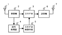
以下、この発明の一実施形態について図1乃至図3を用いて説明する。図1は本発明の一実施形態によるレーダ妨害装置を示すブロック構成図、図2は図1に示す記憶手段3の具体的構成を示すブロック構成図である。図1において、1は周囲環境から到来した到来電波を受信する受信空中線、2は受信空中線1により受信された到来電波について増幅及び検波等の受信処理を行う受信機、3は受信機2により受信処理された受信信号を高速サンプリングし、メモリ等にデジタル的に記憶するDRFM(Digital Radio Frequency Memory。以下、記憶手段という。)、4は受信機2により受信処理された受信信号から到来電波の電波諸元を測定する信号処理手段、5は受信機2からの記憶トリガに基づいて記憶手段3の記憶動作を制御すると共に、信号処理手段4により測定された到来電波の電波諸元に基づいて記憶手段3に記憶された受信信号の再生動作を制御するDRFM制御手段(以下、記憶/再生制御手段という。)、6は記憶/再生制御手段5の制御に基づいて再生された再生信号を増幅処理する送信機、7は送信機6によって増幅処理された再生信号を妨害電波として空間に送信する送信空中線である。
【0016】
また、図2において、8は受信機2から出力された受信信号をデジタル信号に変換するA/D変換器、9はA/D変換器8によりデジタル信号に変換された受信信号を記憶するメモリ等の記憶部、10は記憶部9から再生された再生信号、すなわちデジタル受信信号を、アナログ信号に変換するD/A変換器、11は基準クロック信号を発生するクロック発生手段、12はクロック発生手段11から供給された基準クロック信号及び記憶/再生制御手段からの制御信号に基づいて受信機2から出力された受信信号を記憶部9に記憶させる書込手段、13はクロック発生手段11から出力された基準クロック信号の周波数を可変とするクロック変更手段、14はクロック変更手段13から供給されたクロック信号及び記憶/再生制御手段からの制御信号に基づいて記憶部9に記憶された記憶信号、すなわちデジタル受信信号を再生する再生手段である。
【0017】
なお、この実施の形態によるレーダ妨害装置では、基準クロック信号の周波数を可変とするクロック変更手段13により送信空中線7から送信される妨害信号に周波数変位を与えるタイミング制御手段を構成しているが、このような構成に限られるものではなく、例えば、基準クロック信号と異なる周波数のクロック信号を発生する別のクロック発生手段を設け、このクロック発生手段から供給されるクロック信号に基づいて再生手段14による再生動作、すなわちデジタル受信信号の再生タイミングを書込手段12における記憶タイミングと異ならせるようにしてもよい。
【0018】
次に動作について図3を用いて詳細に説明する。図3は受信機2から出力された受信信号の記憶手段3における記憶動作ないし再生動作を説明する動作原理説明図であって、図3(a)は書込手段12による受信信号の記憶動作を説明する信号波形図、図3(b)は再生手段14によるデジタル受信信号の再生動作を説明する信号波形図である。図3(a)の上段は受信機2から出力された受信信号の例、図3(a)の下段は上段に示す受信信号をA/D変換8によりデジタル化したデジタル受信信号を示しており、また、図3(b)の上段は記憶部9から再生されたデジタル受信信号の例、図3(b)の下段は上段に示すデジタル受信信号をD/A変換器10によりアナログ化した再生信号をそれぞれ示している。
【0019】
まず、受信空中線1により受信された到来電波は受信機2により受信処理される。受信機2では増幅・検波処理がなされ、そのビデオ信号が信号処理手段4に出力される。信号処理手段4は受信機2から出力されたビデオ信号に基づいて到来電波の電波諸元を測定する。測定された到来電波の電波諸元は記憶/再生制御手段5に出力される。このビデオ信号から測定できる電波諸元としては、周波数、パルス幅、パルス繰り返し周波数、スキャン間隔等がある。一方、受信機2により増幅処理された受信信号は記憶手段3に出力され、A/D変換器8によりデジタル化されて記憶部9に記憶される。図2に示すように、記憶手段3の書込手段12にはクロック発生手段11から出力された基準クロック信号と記憶/再生制御手段5からの制御信号とが入力されており、クロック発生手段11から出力された基準クロック信号に基づいてA/D変換器8に対するA/D変換タイミング、及び記憶部9に対する記憶タイミング、すなわちサンプリングタイミングが与えられている。
【0020】
このように、受信機2から出力された受信信号、例えば、図3(a)上段に示すような受信信号15はクロック発生手段11の基準クロック信号のクロック周波数に基づきデジタル化され、図3(a)下段に示すようなデジタル受信信号16として記憶部8に記憶される。なお、この実施の形態によるレーダ妨害装置では、受信機2により増幅された受信信号(RF信号)がそのまま記憶手段3に入力されているが、IF信号に周波数変換してから記憶手段3に入力させるように構成してもよい。
【0021】
次に、記憶部9に記憶されたデジタル受信信号の再生動作について説明する。記憶部9に記憶されたデジタル受信信号16は再生手段14からのタイミング信号に基づいて読み出される。再生手段14にはタイミング制御手段13から出力されたクロック信号と記憶/再生制御手段5から出力された後述の制御信号とが入力されており、タイミング制御手段13から出力されたクロック信号のクロック周波数に基づいて記憶部9に対する再生タイミングが与えられている。なお、タイミング制御手段13はクロック発生手段11から出力された基準クロック信号のクロック周波数を可変とするものであり、これにより基準クロック信号と異なるクロック周波数のクロック信号を再生手段14に出力することができる。
【0022】
記憶部9に記憶されたデジタル受信信号16は書込手段12の記憶タイミングと異なる再生タイミングにより記憶部9から読み出され、図3(b)上段に示すようなデジタル受信信号17として再生される。そして、再生手段14により読み出されたデジタル受信信号17は、D/A変換器10によりアナログ変換され、図3(b)下段に示すような再生信号18となる。図3(b)下段に示すように、D/A変換器10によりアナログ変換された再生信号18は図3(a)上段に示す受信機2から出力された受信信号15に対して波長が短くなっている。このように、記憶部9に記憶されたデジタル受信信号16をタイミング制御手段13から出力されたクロック信号に基づいて再生することにより、再生信号18に対して周波数変位を与えることができる。
【0023】
D/A変換器10によりアナログ変換された再生信号18は送信機6に出力され、増幅処理される。送信機6により増幅処理された再生信号18は、妨害信号として送信空中線7から空間に送信される。なお、再生手段14は、記憶/再生制御手段5からの制御信号、すなわち信号処理手段4により測定された電波諸元に基づく制御信号が入力されており、この制御信号に基づいて記憶部9に記憶されたデジタル受信信号の変調をも行っている。具体的には、記憶部9に記憶されたデジタル受信信号を読み出すタイミング(ON/OFFのタイミング)を記憶/再生制御手段5からの電波諸元に基づく制御信号により制御してパルス幅、パルス間隔及びスキャン間隔の変調を行っている。これにより、送信空中線7から空間に送信される妨害信号の電波諸元を受信空中線1により受信した到来電波の電波諸元に設定することができる。
【0024】
以上のように、この実施形態1によるレーダ妨害装置によれば、再生手段14が記憶/再生制御手段5からの制御信号及びタイミング制御手段13から出力されたクロック信号に基づいて記憶部9に記憶された受信信号の再生ないしD/A変換器10の制御を行うので、送信空中線7から空間に送信される妨害信号の電波諸元を到来電波の電波諸元に設定することができると共に、この妨害信号にタイミング制御手段13から出力されたクロック信号に基づく周波数変位、すなわち速度変化を与えることができる。このように、所望の速度変化を模擬した妨害信号を送信することにより、距離及び方位方向だけでなく、速度変化をも模擬した妨害信号を送信することができ、電波源においてより真の目標と誤認識させることができる妨害信号を送信することができる。
【0025】
なお、この実施の形態によるレーダ妨害装置では、妨害信号の速度変化が速くなるように周波数変位を設定したが、速度変化が遅くなるように設定することもできる。また、妨害信号に与えられる速度変化の量もタイミング制御手段13から出力されるクロック信号のクロック周波数を可変とすることにより所望の速度変化に設定することができる。
【0026】
実施の形態2.
次にこの発明の実施の形態2について図4乃至図6を用いて説明する。実施の形態1によるレーダ妨害装置では、記憶手段3に記憶された受信信号をタイミング変更手段13からのクロック信号に基づいて再生することにより、送信空中線6から出力される妨害信号に所望の速度変化を設定するようにしていたが、受信空中線1により受信された到来電波の受信信号を周波数変換し、この周波数変換されたスペクトル信号に周波数変位を与えて妨害電波に所望の速度変化を設定するようにしてもよい。この実施の形態2によるレーダ妨害装置は、周波数変換した信号に所望の周波数変位を与え、この周波数変位の与えられた信号を再生して妨害信号とするものである。
【0027】
図4はこの実施形態2によるレーダ妨害装置を示すブロック構成図、図5は図1に示す記憶/再生制御手段5の具体的構成を示すブロック構成図である。図4及又は図5において、3b及び5bはこの実施の形態によるレーダ妨害装置の記憶手段及び記憶/再生制御手段、19は記憶手段3bの記憶部9に記憶されたデジタル受信信号を周波数変換し、この周波数変換された信号に所望の周波数変位を与えて妨害信号の速度変化を設定するデジタルシグナルプロセッサ(以下、DSPという。)、20はDSP19の内部に構成された高速フーリエ変換回路(以下、FT回という。)、21はFT回路20により周波数変換されたスペクトル信号に所望の速度変化に対応した周波数変位を与える周波数変更手段、22は周波数変更手段21により周波数変位の与えられたスペクトル信号を逆周波数変換する逆フーリエ変換回路(以下、逆FT回路という。)である。なお、図中、同一符号は同一又は相当部分を示し、これらについての詳細な説明は省略する。
【0028】
次に動作について説明する。受信空中線1により受信された到来電波は受信機2により受信処理された後、記憶手段3bに出力され、A/D変換器8によりデジタル化されて記憶部9に記憶される。記憶部9に記憶されたデジタル受信信号は記憶/再生制御手段5b内に設けられたDSP19に出力され、ここで、送信空中線7から送信される妨害信号に所望の速度変化を設定する処理が行われる。一方、信号処理手段4では受信機2から出力されたビデオ信号に基づいて到来電波の電波諸元が測定され、測定された到来電波の電波諸元は記憶/再生制御手段5bに出力される。
【0029】
次にDSP19の処理について図6を用いて詳細に説明する。図6はDSP19の処理内容を説明する動作原理説明図であって、図6(a)はFT回路20により周波数軸上の信号に変換された受信信号の例を示す周波数特性図、図6(b)は周波数変更手段21による周波数変位の設定について示す周波数特性図である。DSP19に出力されたデジタル受信信号は、まずFT回路20により周波数軸上の信号に変換される。図6(a)に示すように、DSP19に出力されたデジタル受信信号をFT回路20によって周波数変換することにより、例えば、周波数f1のスペクトル信号F1が得られる。FT回路20により得られた周波数信号F1は周波数変更手段21に出力され、ここで妨害信号に設定する所望の速度変化に対応した周波数変位が与えられる。
【0030】
図6(b)において、Δfは妨害信号に設定する所望の速度変化に対応した周波数変位であり、このような周波数変位ΔfがFT回路20により周波数変換されたスペクトル信号F1に与えられる。周波数変更手段21により周波数変位が与えられたスペクトル信号は逆FT回路22に出力され、ここで時間軸上の信号に逆変換される。そして、逆FT回路22により逆変換された信号は再生手段13により再生される信号として記憶部9に記憶された受信信号と書き替えられる。このように、DSP19における処理により送信空中線7から送信される妨害信号に対して周波数変位の変調を行うことができる。
【0031】
記憶部9に書き替えられたデジタル受信信号は再生手段14からのタイミング信号に基づき再生される。再生手段14にはクロック発生手段11からの基準クロック信号が入力されているが、記憶/再生制御手段5から出力された制御信号が入力されており、DSP19の周波数変更手段21により与えられた周波数変位、及び信号処理手段4により測定された電波諸元に基づく制御信号が入力されており、これらに基づく再生タイミングにより記憶部8に書き替えられたデジタル受信信号を再生する。これにより、送信空中線7から空間に送信される妨害信号の電波諸元を受信空中線1により受信した到来電波の電波諸元に設定することができると共に、妨害信号に所望の速度変化を設定することができる。
【0032】
再生されたデジタル受信信号はD/A変換器10によりアナログ変換され、送信機7に出力される。送信機6に出力された再生信号は増幅処理され、妨害信号として送信空中線7から空間に送信される。
【0033】
以上のように、この実施形態2によるレーダ妨害装置によれば、送信空中線7から空間に送信される妨害信号に設定する速度変化をDSP19の処理により行うので、記憶手段3bにおいてタイミング変更手段13を設けることなく、所望の速度変化を模擬した妨害信号を送信することができる。これにより、上記実施の形態1によるレーダ妨害装置と同様に、距離及び方位方向だけでなく、速度変化をも模擬した妨害信号を送信することができ、電波源においてより真の目標と誤認識させることができる妨害信号を送信することができる。
【0034】
また、DSP19の処理により妨害信号に対する速度変化の設定を行うことにより、実施の形態1によるレーダ妨害装置のように記憶手段3bにタイミング変更手段13を設ける必要がなく、いわゆるハード構成が大型化することを防止することができる。なお、この実施の形態2によるレーダ妨害装置では、DSP19は記憶/再生制御手段5の内部に設けるように構成したが、DSP19を記憶/再生制御手段5bに外付けするように構成してもよい。
【0035】
実施の形態3.
次にこの発明の実施の形態3について図7を用いて説明する。実施の形態2によるレーダ妨害装置では、DSP19の処理により妨害信号に対する速度変化の設定を行い、到来電波の電波諸元については信号処理手段4の処理により測定を行っていたが、これら到来電波の電波諸元の測定をDSP19の処理により行うように構成してもよい。この実施の形態3によるレーダ妨害装置は、DSPの処理により妨害信号に対する速度変化の設定、及び到来電波の電波諸元の測定を行うものである。
【0036】
図7はこの実施形態3によるレーダ妨害装置を示すブロック構成図である。図7において、3c及び5cはこの実施の形態によるレーダ妨害装置の記憶手段及び記憶/再生制御手段、19cは記憶手段3cの記憶部9に記憶されたデジタル受信信号から到来電波の周波数、パルス幅、パルス繰り返し周波数、スキャン間隔等の電波諸元を求めると共に、送信空中線7から送信される妨害信号に対して所望の速度変化の設定を行うデジタルシグナルプロセッサ(以下、DSPという。)である。このDSP19cは、図5に示すようなFT回路20、周波数変更手段21及び逆FT回路22を有すると共に、さらに記憶手段3cの記憶部9に記憶されたデジタル受信信号から到来電波の各種電波諸元の測定を行う電波諸元測定手段(図示省略する。)を有している。なお、図中、同一符号は同一又は相当部分を示し、これらについての詳細な説明は省略する。
【0037】
次に動作について説明する。受信空中線1により受信された到来電波は受信機2により受信処理された後、記憶手段3cに出力され、A/D変換器8によりデジタル化されて記憶部9に記憶される。この際、記憶部9に記憶されるデジタル受信信号は1パルス分の受信信号ではなく、数パルス分の受信信号についてA/D変換されたデジタル受信信号が記憶される。これにより、到来電波の周波数、パルス幅、さらにはパルス繰り返し周波数、スキャン間隔についてDSP19cにより測定を行うことが可能となる。記憶部9に記憶されたこのようなデジタル受信信号は、記憶/再生制御手段5b内に設けられたDSP19cに出力され、ここで、到来電波の電波諸元を測定する処理、及び送信空中線7から送信される妨害信号に所望の速度変化を設定する処理が行われる。
【0038】
次にDSP19cの処理について説明する。DSP19cに出力されたデジタル受信信号は、FT回路20、周波数変更手段21及び逆FT回路22により妨害信号に設定する所望の速度変化に対応した周波数変位が与えられ、再生手段13により再生される信号として記憶部9に記憶された受信信号と書き替えられる。また、電波諸元測定手段に出力され、到来電波の周波数、パルス幅、パルス繰り返し周波数、スキャン間隔が測定される。
【0039】
記憶部9に書き替えられたデジタル受信信号は再生手段14からのタイミング信号に基づき再生される。再生手段14にはクロック発生手段11からの基準クロック信号と記憶/再生制御手段5から出力された制御信号とが入力されており、DSP19cの周波数変更手段21により与えられた周波数変位、及び電波諸元測定手段により測定された電波諸元に基づく制御信号による再生タイミングにより記憶部8に書き替えられたデジタル受信信号を再生する。これにより、送信空中線7から空間に送信される妨害信号の電波諸元を受信空中線1により受信した到来電波の電波諸元に設定することができると共に、妨害信号に所望の速度変化を設定することができる。
【0040】
再生されたデジタル受信信号はD/A変換器10によりアナログ変換され、送信機7に出力される。送信機6に出力された再生信号は増幅処理され、妨害信号として送信空中線7から空間に送信される。
【0041】
以上のように、この実施形態3によるレーダ妨害装置によれば、上記実施の形態によるレーダ妨害装置と同様に、距離及び方位方向だけでなく、速度変化をも模擬した妨害信号を送信することができ、電波源においてより真の目標と誤認識させることができる妨害信号を送信することができる。また、DSP19cの処理により到来電波の電波諸元の測定を行うことにより、実施の形態2によるレーダ妨害装置のように到来電波の電波諸元を測定する信号処理手段を設ける必要がなく、さらにハード構成を小型化したレーダ妨害装置を得ることができる。なお、この実施の形態3によるレーダ妨害装置においてもDSP19cを記憶/再生制御手段5cに外付けするように構成してもよい。
【0042】
実施の形態4.
次にこの発明の実施の形態4について図8を用いて説明する。上記実施の形態2,3によるレーダ妨害装置のように、DRFM等の記憶手段の記憶部9には受信機2により受信処理された受信信号がデジタル化されて記憶されるので、到来電波の電波諸元の測定、妨害信号に設定する速度変化に対応した周波数変位の変調をDSPによるソフトウェア処理により行うことが可能であり、これによりハード構成を大幅に小型化することができる。この実施の形態4によるレーダ妨害装置はDRFM等の記憶手段の機能をもDSPに持たせることにより、レーダ妨害装置のハード構成をさらに小型化するものである。
【0043】
図8はこの実施形態4によるレーダ妨害装置を示すブロック構成図である。図8において、5dはこの実施の形態によるレーダ妨害装置の記憶/再生制御手段、19dは実施の形態3によるレーダ妨害装置のDSP19cに、さらにDRFM等の記憶手段の機能、すなわちA/D変換機能、D/A変換機能等を持たせたデジタルシグナルプロセッサ(以下、DSPという。)である。記憶部9についてはDSP19d内に設けられたメモリ(図示省略する。)を使用すればよい。このDSP19dは、図5に示すようなFT回路20、周波数変更手段21及び逆FT回路22を有すると共に、さらにDSP19d内に設けられたメモリに記憶されたデジタル受信信号から到来電波の各種電波諸元の測定を行う電波諸元測定手段(図示省略する。)を有している。なお、図中、同一符号は同一又は相当部分を示し、これらについての詳細な説明は省略する。
【0044】
以上のように、この実施形態4によるレーダ妨害装置によれば、上記実施の形態によるレーダ妨害装置と同様に、距離及び方位方向だけでなく、速度変化をも模擬した妨害信号を送信することができ、電波源においてより真の目標と誤認識させることができる妨害信号を送信することができる。また、DSP19dにDRFM等の記憶手段の機能を持たせることにより、実施の形態3によるレーダ妨害装置のように受信機2により受信処理された受信信号を記憶させるDRFM等の記憶手段を設ける必要がなく、さらにハード構成を小型化したレーダ妨害装置を得ることができる。なお、この実施の形態3によるレーダ妨害装置においてもDSP19dを記憶/再生制御手段5dに外付けするように構成してもよい。
【0045】
実施の形態5.
次にこの発明の実施の形態5について図9を用いて説明する。上記実施の形態によるレーダ妨害装置では、DRFM等の記憶手段3を一つだけ設けており、1波の妨害信号を送信するものついて説明したが、到来電波は1種類だけでなく、かつ、複数方向から到来する場合もある。この実施の形態5によるレーダ妨害装置は、複数の妨害信号を送信するものである。
【0046】
図9はこの実施形態5によるレーダ妨害装置を示すブロック構成図である。図9において、5eはこの実施の形態によるレーダ妨害装置の記憶/再生制御手段、23はDRFM等の記憶手段3eを複数設けた記憶装置である。記憶装置23に設けられた各記憶手段3eは各到来電波に対する受信信号の記憶/再生を行うものであり、設けられた記憶手段3eの数だけ妨害信号を送信することが可能である。また、記憶/再生制御手段5eは受信機2からの記憶トリガに基づいて各記憶手段3eの記憶動作を制御すると共に、信号処理手段4により測定された各到来電波の電波諸元に基づいて各記憶手段3eに記憶された受信信号の再生動作を制御する。なお、図中、同一符号は同一又は相当部分を示し、これらについての詳細な説明は省略する。
【0047】
次に動作について説明する。受信空中線1により受信された複数の到来電波は受信機2によって順次受信処理される。受信機2により受信処理された各ビデオ信号は信号処理手段4に出力され、ここで各到来電波の電波諸元がそれぞれ測定される。測定された各到来電波の電波諸元は記憶/再生制御手段5eに出力される。一方、受信機2により増幅処理された各受信信号は順次記憶装置23に出力され、対応する記憶手段3eにそれぞれ入力される。各記憶手段3eに入力された受信信号は実施の形態1による記憶手段3と同様に記憶部9に記憶され、各記憶手段3eに設けられたタイミング制御手段(図示省略する。)からのクロック信号、及び記憶/再生制御手段5eからの制御信号に基づいてそれぞれ再生される。
【0048】
再生された各デジタル受信信号はそれぞれアナログ変換され、送信機7に出力される。送信機6に出力された各再生信号はそれぞれ増幅処理され、妨害信号として送信空中線7から空間に送信される。このように、この実施形態4によるレーダ妨害装置によれば、受信空中線1により複数の到来電波が受信される場合であっても、各到来電波に対して実施の形態1によるレーダ妨害装置と同様に、距離及び方位方向だけでなく、速度変化をも模擬した妨害信号を送信することができ、複数の電波源においてより真の目標と誤認識させることができる妨害信号を送信することができる。
【0049】
なお、図9に示すレーダ妨害装置は、実施の形態1によるレーダ妨害装置を複数波用に構成したものであるが、DSPを設けた他の実施の形態によるレーダ妨害装置、例えば、図4、図7及び図8に示すようなレーダ妨害装置を複数波用に構成してもよい。例えば、図4に示すレーダ妨害装置に対応する構成としては、記憶装置23内に複数の記憶手段3bを設け、これら記憶手段3bに対応する複数のDSP19を記憶/再生制御手段5bに設けるようにすればよい。
【0050】
なお、以上のように、受信機2により受信処理された受信信号をデジタル化して記憶するように構成することにより、到来電波の電波諸元の測定等をソフトウェア処理により行うことができ、いわゆるハード構成を大幅に小型化することが可能となるが、反面、DSPを多機能化させることが必要となる。したがって、この発明に係るレーダ妨害装置を実施する際には実施数等に応じて適宜最適な実施の形態を選択すればよい。
【0051】
【発明の効果】
以上のように、この発明によれば、記憶部に記憶されたデジタル受信信号をスペクトラム信号に変換し、そのスペクトル信号の周波数に周波数変位を与え、その周波数変位の与えられたスペクトル信号をデジタル受信信号に逆変換して前記記憶部に記憶し、その逆変換され前記記憶部に記憶されたデジタル受信信号から前記到来電波の電波諸元に基づく再生信号を再生するので、クロック信号のタイミング制御手段等が不要となり、ハード構成を小型化できる一方、電波源においてより真の目標と誤認識させることができる妨害信号を送信することができる。
【図面の簡単な説明】
【図1】 この発明の実施の形態1によるレーダ妨害装置を示すブロック構成図である。
【図2】 図1に示す記憶手段3の具体的構成を示すブロック構成図である。
【図3】 記憶手段3における記憶動作ないし再生動作を説明する動作原理説明図である。
【図4】 この発明の実施の形態2によるレーダ妨害装置を示すブロック構成図である。
【図5】 図4に示すDSP19の具体的構成を示すブロック構成図である。
【図6】 DSP19の処理内容を説明する動作原理説明図である。
【図7】 この発明の実施の形態3によるレーダ妨害装置を示すブロック構成図である。
【図8】 この発明の実施の形態4よるレーダ妨害装置を示すブロック構成図である。
【図9】 この発明の実施の形態5によるレーダ妨害装置を示すブロック構成図である。
【符号の説明】
1 受信空中線、2 受信機、3,3b,3c,3e 記憶手段、
4 信号処理手段、5,5b,5c,5d,5e 記憶/再生制御手段、
6 送信機、7 送信空中線、
9 記憶部、12 書込手段、13 タイミング制御手段、14 再生手段、
19,19c,19d DSP(演算手段)。
[0001]
BACKGROUND OF THE INVENTION
The present invention relates to a radar jamming apparatus that transmits jamming radio waves to a radio wave source.
[0002]
[Prior art]
In general, this type of radar jamming apparatus receives an incoming radio wave from an antenna and transmits the jamming radio wave to a radio wave source based on the received incoming radio wave. For example, in Japanese Patent Laid-Open No. 9-264945, a received pulse signal of an incoming radio wave is stored in a device called DRFM (Digital Radio Frequency Memory: hereinafter referred to as DRFM), and based on the pulse signal stored in the DRFM. That transmit jamming radio waves.
[0003]
In addition, the pulse frequency, pulse width, pulse repetition frequency, and scan interval of the incoming radio waves are measured from the video signal detected by the receiver, and the radio wave specifications of the jamming radio wave are set based on these radio wave specifications.
[0004]
[Problems to be solved by the invention]
However, since the conventional radar jamming apparatus is configured as described above, it can transmit the jamming radio wave simulated in the distance direction or the azimuth direction based on the measured radio wave specifications, but the speed change and There is a problem in that it is not possible to transmit a jamming radio wave that is simulated for intra-pulse modulation such as pulse compression, and it is easy to identify whether it is a jamming radio wave or not by measuring the speed change on the radio wave source side.
[0005]
The present invention has been made to solve the above-described problems, and can transmit a jamming signal that makes it difficult to identify whether or not it is a jamming radio wave. It is an object of the present invention to provide a novel radar jamming device that can be misrecognized as if it were a true target.
[0006]
It is another object of the present invention to provide a more compact radar jamming device that can prevent a so-called hardware configuration from increasing in size.
[0007]
[Means for Solving the Problems]
A radar interfering device according to the invention of claim 1 is a receiving means for receiving incoming radio waves, a signal processing means for measuring radio wave specifications of the incoming radio waves from a received signal of the receiving means, and a received signal of the receiving means. A / D converter for converting the digital received signal into a digital received signal, a storage unit for storing the digital received signal, an FFT circuit for converting the digital received signal stored in the storage unit into a spectrum signal, and the F F A frequency changing means for giving a frequency displacement to the frequency of the spectrum signal output from the T circuit, an inverse FFT circuit for inversely converting the spectrum signal to which the frequency displacement has been given into a digital reception signal and storing it in the storage unit; Control means for reproducing a reproduction signal based on radio wave specifications of the incoming radio wave from a digital reception signal that has been inversely converted and stored in the storage unit, a D / A converter for analog conversion of the reproduction signal, and the analog conversion And transmission means for transmitting an interference signal by the reproduced signal.
[0008]
A radar interfering device according to the invention of claim 2 is a receiving means for receiving and processing a plurality of incoming radio waves, a signal processing means for measuring radio wave specifications of the plurality of incoming radio waves from each received signal of the receiving means, An A / D converter that converts each received signal of the receiving means into a digital received signal for each incoming radio wave, a storage unit that stores each digital received signal, and each digital received signal stored in this storage unit is a spectrum. FFT circuit for converting to a signal, and this F F Frequency changing means for giving a frequency displacement to the frequency of each spectrum signal output from the T circuit, and an inverse FFT for inversely converting each spectrum signal to which the frequency displacement has been given into a digital reception signal and storing it in the storage unit A circuit, control means for regenerating the reproduction signals based on the radio wave specifications of the plurality of incoming radio waves from the digital reception signals that are inversely converted and stored in the storage unit, and D / A converter is provided, and a transmission means for transmitting a plurality of disturbing signals by each of the analog-converted reproduction signals.
[0009]
A radar jamming device according to the invention of claim 3 is: Receiving means for receiving incoming radio waves, an A / D converter for converting the received signal of the receiving means into a digital signal, a storage unit for storing the digital received signal, and a digital received signal stored in the storage unit A function for measuring the radio wave specifications of the incoming radio wave, a function for converting a digital reception signal stored in the storage unit into a spectrum signal, a function for giving a frequency displacement to the frequency of the spectrum signal, and a function for giving the frequency displacement A computing means having a function of inversely converting the spectrum signal into a digital received signal and storing it in the storage section; and a radio wave of the incoming radio wave from the digital reception signal inversely converted by the function of the computing means and stored in the storage section Control means for reproducing a reproduction signal based on specifications, a D / A converter for analog conversion of the reproduction signal, and the analog-converted reproduction signal Transmitting means for transmitting the interfering signal by It is equipped with.
[0010]
A radar jamming device according to the invention of claim 4 The A / D converter, the storage unit, and the D / A converter Of the computing means Provided internally, and stored in the storage unit digital received signals for a plurality of pulses converted by the A / D converter. Is.
[0011]
A radar jamming device according to the invention of claim 5 is: The arithmetic means is a DSP circuit. Is.
[0015]
DETAILED DESCRIPTION OF THE INVENTION
Embodiment 1 of the Invention
An embodiment of the present invention will be described below with reference to FIGS. FIG. 1 is a block configuration diagram showing a radar jamming apparatus according to an embodiment of the present invention, and FIG. 2 is a block configuration diagram showing a specific configuration of the storage means 3 shown in FIG. In FIG. 1, reference numeral 1 is a reception antenna that receives an incoming radio wave that has arrived from the surrounding environment, 2 is a receiver that performs reception processing such as amplification and detection on the incoming radio wave that is received by the reception antenna 1, and 3 is received by a receiver 2. DRFM (Digital Radio Frequency Memory; hereinafter referred to as storage means) that samples the processed received signal at high speed and stores it digitally in a memory or the like, 4 is the radio wave of the incoming radio wave from the received signal received by the receiver 2 The signal processing means 5 for measuring the specifications controls the storage operation of the storage means 3 based on the storage trigger from the receiver 2 and stores it based on the radio wave specifications of the incoming radio waves measured by the signal processing means 4. DRFM control means for controlling the reproduction operation of the received signal stored in the means 3 (hereinafter referred to as storage / reproduction control means), 6 Transmitter a signal reproduced based on the control of the storage / reproduction control means 5 for amplification, 7 is a transmitting antenna for transmitting the space reproduction signal amplified processed by transmitter 6 as jammers.
[0016]
In FIG. 2, reference numeral 8 denotes an A / D converter that converts a received signal output from the receiver 2 into a digital signal, and reference numeral 9 denotes a memory that stores the received signal converted into a digital signal by the A / D converter 8. 10 is a D / A converter that converts a reproduction signal reproduced from the storage unit 9, that is, a digital reception signal, into an analog signal, 11 is a clock generation means that generates a reference clock signal, and 12 is a clock generator. Write means for storing the received signal output from the receiver 2 in the storage unit 9 based on the reference clock signal supplied from the means 11 and the control signal from the storage / reproduction control means, and 13 outputs from the clock generation means 11 A clock changing means for changing the frequency of the reference clock signal, 14 is a clock signal supplied from the clock changing means 13 and a storage / reproduction control means; It stored memory signal in the storage unit 9 based on the control signal, that is, reproducing means for reproducing a digital reception signal.
[0017]
In the radar jamming apparatus according to this embodiment, a timing control unit is provided that gives a frequency displacement to the jamming signal transmitted from the transmission antenna 7 by the clock changing unit 13 that makes the frequency of the reference clock signal variable. The present invention is not limited to such a configuration. For example, another clock generating means for generating a clock signal having a frequency different from that of the reference clock signal is provided, and the reproducing means 14 is based on the clock signal supplied from the clock generating means. The reproduction operation, that is, the reproduction timing of the digital reception signal may be different from the storage timing in the writing unit 12.
[0018]
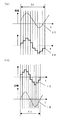
Next, the operation will be described in detail with reference to FIG. FIG. 3 is a diagram for explaining the operation principle for explaining the storing operation or the reproducing operation in the storage means 3 of the received signal output from the receiver 2. FIG. 3 (a) shows the storing operation of the received signal by the writing means 12. FIG. 3B is a signal waveform diagram for explaining the reproduction operation of the digital reception signal by the reproducing means 14. The upper part of FIG. 3A shows an example of a reception signal output from the receiver 2, and the lower part of FIG. 3A shows a digital reception signal obtained by digitizing the reception signal shown in the upper part by A / D conversion 8. 3B is an example of a digital reception signal reproduced from the storage unit 9, and the lower part of FIG. 3B is a reproduction obtained by converting the digital reception signal shown in the upper part into an analog form by the D / A converter 10. Each signal is shown.
[0019]
First, an incoming radio wave received by the receiving antenna 1 is received and processed by the receiver 2. The receiver 2 performs amplification and detection processing, and the video signal is output to the signal processing means 4. The signal processing means 4 measures the radio wave specifications of the incoming radio wave based on the video signal output from the receiver 2. The measured radio wave specifications are output to the storage / reproduction control means 5. Radio wave specifications that can be measured from this video signal include frequency, pulse width, pulse repetition frequency, scan interval, and the like. On the other hand, the received signal amplified by the receiver 2 is output to the storage means 3, digitized by the A / D converter 8, and stored in the storage unit 9. As shown in FIG. 2, the writing means 12 of the storage means 3 is supplied with the reference clock signal output from the clock generation means 11 and the control signal from the storage / reproduction control means 5. The A / D conversion timing for the A / D converter 8 and the storage timing for the storage unit 9, that is, the sampling timing, are given based on the reference clock signal output from.
[0020]
In this way, the reception signal output from the receiver 2, for example, the reception signal 15 as shown in the upper part of FIG. a) It is stored in the storage unit 8 as a digital reception signal 16 as shown in the lower part. In the radar jamming apparatus according to this embodiment, the received signal (RF signal) amplified by the receiver 2 is inputted as it is to the storage means 3, but after being converted into an IF signal, it is inputted to the storage means 3. You may comprise.
[0021]
Next, the reproduction operation of the digital reception signal stored in the storage unit 9 will be described. The digital reception signal 16 stored in the storage unit 9 is read based on the timing signal from the reproduction means 14. The reproduction means 14 receives a clock signal output from the timing control means 13 and a control signal described later output from the storage / reproduction control means 5, and the clock frequency of the clock signal output from the timing control means 13. The reproduction timing for the storage unit 9 is given based on the above. Note that the timing control means 13 makes the clock frequency of the reference clock signal output from the clock generation means 11 variable, so that a clock signal having a clock frequency different from the reference clock signal can be output to the reproduction means 14. it can.
[0022]
The digital reception signal 16 stored in the storage unit 9 is read from the storage unit 9 at a reproduction timing different from the storage timing of the writing means 12 and reproduced as a digital reception signal 17 as shown in the upper part of FIG. . The digital reception signal 17 read by the reproduction means 14 is converted into an analog signal by the D / A converter 10 to become a reproduction signal 18 as shown in the lower part of FIG. As shown in the lower part of FIG. 3B, the reproduction signal 18 analog-converted by the D / A converter 10 has a shorter wavelength than the reception signal 15 output from the receiver 2 shown in the upper part of FIG. It has become. Thus, by reproducing the digital reception signal 16 stored in the storage unit 9 based on the clock signal output from the timing control means 13, it is possible to give a frequency displacement to the reproduction signal 18.
[0023]
The reproduction signal 18 analog-converted by the D / A converter 10 is output to the transmitter 6 and amplified. The reproduced signal 18 amplified by the transmitter 6 is transmitted from the transmission antenna 7 to the space as an interference signal. The reproduction means 14 receives a control signal from the storage / reproduction control means 5, that is, a control signal based on the radio wave specifications measured by the signal processing means 4, and the storage section 9 receives the control signal based on this control signal. The stored digital received signal is also modulated. Specifically, the timing (ON / OFF timing) for reading the digital reception signal stored in the storage unit 9 is controlled by a control signal based on radio wave specifications from the storage / reproduction control means 5 to control the pulse width and pulse interval. In addition, the scan interval is modulated. Thereby, the radio wave specification of the interference signal transmitted from the transmission antenna 7 to the space can be set to the radio wave specification of the incoming radio wave received by the reception antenna 1.
[0024]
As described above, according to the radar jamming apparatus according to the first embodiment, the reproduction unit 14 stores in the storage unit 9 based on the control signal from the storage / reproduction control unit 5 and the clock signal output from the timing control unit 13. Since the received signal is reproduced or the D / A converter 10 is controlled, the radio wave specification of the interference signal transmitted from the transmission antenna 7 to the space can be set as the radio wave specification of the incoming radio wave. A frequency displacement based on the clock signal output from the timing control means 13, that is, a speed change can be given to the interference signal. In this way, by transmitting a disturbing signal that simulates a desired speed change, it is possible to transmit a disturbing signal that simulates not only the distance and azimuth direction but also the speed change. Interference signals that can be misrecognized can be transmitted.
[0025]
In the radar jamming apparatus according to this embodiment, the frequency displacement is set so that the speed change of the jamming signal becomes fast. However, it can be set so that the speed change becomes slow. The amount of speed change given to the interference signal can also be set to a desired speed change by making the clock frequency of the clock signal output from the timing control means 13 variable.
[0026]
Embodiment 2. FIG.
Next, a second embodiment of the present invention will be described with reference to FIGS. In the radar jamming apparatus according to the first embodiment, the received signal stored in the storage means 3 is reproduced based on the clock signal from the timing changing means 13, so that a desired speed change is made to the jamming signal output from the transmission antenna 6. However, frequency conversion is performed on the received signal of the incoming radio wave received by the receiving antenna 1, and a frequency change is applied to the frequency-converted spectrum signal to set a desired speed change in the jamming radio wave. It may be. The radar jamming apparatus according to the second embodiment gives a desired frequency displacement to the frequency-converted signal, and reproduces the signal given the frequency displacement to obtain a jamming signal.
[0027]
FIG. 4 is a block diagram showing a radar jamming apparatus according to the second embodiment, and FIG. 5 is a block diagram showing a specific structure of the storage / reproduction control means 5 shown in FIG. 4 and 5, reference numerals 3b and 5b denote storage means and storage / reproduction control means of the radar jamming apparatus according to this embodiment, and 19 denotes frequency conversion of the digital reception signal stored in the storage unit 9 of the storage means 3b. , A digital signal processor (hereinafter referred to as a DSP) that applies a desired frequency displacement to the frequency-converted signal to set a speed change of the interference signal, and 20 is a fast Fourier transform circuit (hereinafter referred to as a DSP) configured in the DSP 19. F F T times Road That's it. ), 21 is F F Frequency changing means for giving a frequency displacement corresponding to a desired speed change to the spectrum signal frequency-converted by the T circuit 20, and 22 an inverse Fourier transform circuit for inversely frequency-converting the spectrum signal given the frequency displacement by the frequency changing means 21 (Hereafter, reverse F F This is called a T circuit. ). In the drawings, the same reference numerals indicate the same or corresponding parts, and detailed description thereof will be omitted.
[0028]
Next, the operation will be described. The incoming radio wave received by the receiving antenna 1 is subjected to reception processing by the receiver 2, then output to the storage means 3 b, digitized by the A / D converter 8, and stored in the storage unit 9. The digital reception signal stored in the storage unit 9 is output to the DSP 19 provided in the storage / reproduction control means 5b, where a process for setting a desired speed change to the disturbing signal transmitted from the transmission antenna 7 is performed. Is called. On the other hand, the signal processing means 4 measures the radio wave specifications of the incoming radio wave based on the video signal output from the receiver 2, and outputs the measured radio wave specifications of the incoming radio wave to the storage / reproduction control means 5b.
[0029]
Next, the processing of the DSP 19 will be described in detail with reference to FIG. FIG. 6 is a diagram for explaining the operating principle for explaining the processing contents of the DSP 19, and FIG. F FIG. 6B is a frequency characteristic diagram showing an example of a received signal converted into a signal on the frequency axis by the T circuit 20, and FIG. The digital reception signal output to the DSP 19 is first F. F The signal is converted into a signal on the frequency axis by the T circuit 20. As shown in FIG. 6A, the digital reception signal output to the DSP 19 is changed to F. F By performing frequency conversion by the T circuit 20, for example, a spectrum signal F1 having a frequency f1 is obtained. F F The frequency signal F1 obtained by the T circuit 20 is output to the frequency changing means 21, where a frequency displacement corresponding to a desired speed change set as an interference signal is given.
[0030]
In FIG. 6B, Δf is a frequency displacement corresponding to a desired speed change set in the interference signal. Such a frequency displacement Δf is F F The spectrum signal F1 frequency-converted by the T circuit 20 is given. The spectrum signal given the frequency displacement by the frequency changing means 21 is the inverse F F The signal is output to the T circuit 22 where it is converted back into a signal on the time axis. And reverse F F The signal inversely converted by the T circuit 22 is rewritten with the received signal stored in the storage unit 9 as a signal reproduced by the reproducing means 13. As described above, the frequency displacement can be modulated on the interference signal transmitted from the transmission antenna 7 by the processing in the DSP 19.
[0031]
The digital received signal rewritten in the storage unit 9 is reproduced based on the timing signal from the reproducing means 14. Although the reference clock signal from the clock generation means 11 is input to the reproduction means 14, the control signal output from the storage / reproduction control means 5 is input, and the frequency given by the frequency changing means 21 of the DSP 19. A control signal based on the displacement and the radio wave specifications measured by the signal processing means 4 is input, and the digital reception signal rewritten in the storage unit 8 is reproduced at the reproduction timing based on these. Thereby, the radio wave specification of the interference signal transmitted from the transmission antenna 7 to the space can be set to the radio wave specification of the incoming radio wave received by the reception antenna 1, and a desired speed change is set to the interference signal. Can do.
[0032]
The reproduced digital reception signal is converted into an analog signal by the D / A converter 10 and output to the transmitter 7. The reproduced signal output to the transmitter 6 is amplified and transmitted from the transmission antenna 7 to the space as an interference signal.
[0033]
As described above, according to the radar jamming apparatus according to the second embodiment, the speed change set in the jamming signal transmitted from the transmitting antenna 7 to the space is performed by the processing of the DSP 19, so the timing changing means 13 is set in the storage means 3b. Without providing, an interference signal simulating a desired speed change can be transmitted. Thereby, similarly to the radar jamming apparatus according to the first embodiment, it is possible to transmit a jamming signal that simulates not only the distance and azimuth direction but also the speed change, and makes the radio wave source misrecognize as a true target. A jamming signal that can be transmitted.
[0034]
Further, by setting the speed change for the interference signal by the processing of the DSP 19, it is not necessary to provide the timing changing means 13 in the storage means 3b unlike the radar interference device according to the first embodiment, and the so-called hardware configuration is increased. This can be prevented. In the radar jamming apparatus according to the second embodiment, the DSP 19 is configured to be provided inside the storage / reproduction control unit 5, but the DSP 19 may be configured to be externally attached to the storage / reproduction control unit 5b. .
[0035]
Embodiment 3 FIG.
Next, Embodiment 3 of the present invention will be described with reference to FIG. In the radar jamming apparatus according to the second embodiment, the speed change for the jamming signal is set by the processing of the DSP 19, and the radio wave specifications of the incoming radio wave are measured by the processing of the signal processing means 4. You may comprise so that a measurement of a radio wave specification may be performed by the process of DSP19. The radar jamming apparatus according to the third embodiment performs setting of a speed change for a jamming signal and measurement of radio wave specifications of incoming radio waves by DSP processing.
[0036]
FIG. 7 is a block diagram showing a radar jamming apparatus according to the third embodiment. In FIG. 7, 3c and 5c are storage means and storage / reproduction control means of the radar jamming apparatus according to this embodiment, and 19c is the frequency and pulse width of the incoming radio wave from the digital received signal stored in the storage unit 9 of the storage means 3c. A digital signal processor (hereinafter referred to as a DSP) that obtains radio wave specifications such as a pulse repetition frequency and a scan interval and sets a desired speed change with respect to an interference signal transmitted from the transmission antenna 7. This DSP 19c has an F as shown in FIG. F T circuit 20, frequency changing means 21 and inverse F F In addition to the T circuit 22, it further includes radio wave specification measuring means (not shown) for measuring various radio wave specifications of the incoming radio wave from the digital reception signal stored in the storage unit 9 of the storage means 3 c. . In the drawings, the same reference numerals indicate the same or corresponding parts, and detailed description thereof will be omitted.
[0037]
Next, the operation will be described. The incoming radio wave received by the receiving antenna 1 is subjected to reception processing by the receiver 2, then output to the storage means 3 c, digitized by the A / D converter 8, and stored in the storage unit 9. At this time, the digital reception signal stored in the storage unit 9 is not a reception signal for one pulse, but a digital reception signal obtained by A / D conversion of reception signals for several pulses. As a result, the DSP 19c can measure the frequency, pulse width, pulse repetition frequency, and scan interval of the incoming radio wave. Such a digital reception signal stored in the storage unit 9 is output to the DSP 19c provided in the storage / reproduction control means 5b. Here, the process of measuring the radio wave specifications of the incoming radio wave, and the transmission antenna 7 A process for setting a desired speed change in the transmitted jamming signal is performed.
[0038]
Next, the processing of the DSP 19c will be described. The digital reception signal output to the DSP 19c is F F T circuit 20, frequency changing means 21 and inverse F F A frequency shift corresponding to a desired speed change set as an interference signal is given by the T circuit 22, and the received signal stored in the storage unit 9 is rewritten as a signal reproduced by the reproducing means 13. Further, it is output to the radio wave specification measuring means, and the frequency, pulse width, pulse repetition frequency and scan interval of the incoming radio wave are measured.
[0039]
The digital received signal rewritten in the storage unit 9 is reproduced based on the timing signal from the reproducing means 14. The reproduction means 14 is supplied with the reference clock signal from the clock generation means 11 and the control signal outputted from the storage / reproduction control means 5, and the frequency displacement given by the frequency changing means 21 of the DSP 19 c and the various radio waves. The digital reception signal rewritten in the storage unit 8 is reproduced at the reproduction timing by the control signal based on the radio wave specifications measured by the original measuring means. Thereby, the radio wave specification of the interference signal transmitted from the transmission antenna 7 to the space can be set to the radio wave specification of the incoming radio wave received by the reception antenna 1, and a desired speed change is set to the interference signal. Can do.
[0040]
The reproduced digital reception signal is converted into an analog signal by the D / A converter 10 and output to the transmitter 7. The reproduced signal output to the transmitter 6 is amplified and transmitted from the transmission antenna 7 to the space as an interference signal.
[0041]
As described above, according to the radar jamming apparatus according to the third embodiment, it is possible to transmit a jamming signal that simulates not only the distance and the azimuth direction but also the speed change, similarly to the radar jamming apparatus according to the above embodiment. It is possible to transmit a jamming signal that can be erroneously recognized as a true target in the radio wave source. Further, by measuring the radio wave specifications of the incoming radio waves by the processing of the DSP 19c, it is not necessary to provide signal processing means for measuring the radio wave specifications of the incoming radio waves unlike the radar jamming apparatus according to the second embodiment, and further, A radar jamming device having a reduced configuration can be obtained. In the radar jamming apparatus according to the third embodiment, the DSP 19c may be externally attached to the storage / reproduction control means 5c.
[0042]
Embodiment 4 FIG.
Next, a fourth embodiment of the present invention will be described with reference to FIG. Like the radar jamming apparatus according to the second and third embodiments, the received signal processed by the receiver 2 is digitized and stored in the storage unit 9 of the storage means such as DRFM. It is possible to perform measurement of specifications and modulation of frequency displacement corresponding to a speed change set for an interference signal by software processing by a DSP, and thereby the hardware configuration can be greatly reduced in size. The radar jamming device according to the fourth embodiment further reduces the hardware configuration of the radar jamming device by providing the DSP with the function of a storage means such as DRFM.
[0043]
FIG. 8 is a block diagram showing a radar jamming apparatus according to the fourth embodiment. In FIG. 8, 5d is the storage / reproduction control means of the radar jammer according to this embodiment, 19d is the DSP 19c of the radar jammer according to the third embodiment, and further the function of the memory means such as DRFM, that is, the A / D conversion function. A digital signal processor (hereinafter referred to as a DSP) having a D / A conversion function or the like. As the storage unit 9, a memory (not shown) provided in the DSP 19d may be used. The DSP 19d has an F as shown in FIG. F T circuit 20, frequency changing means 21 and inverse F F In addition to the T circuit 22, it further includes radio wave specification measuring means (not shown) for measuring various radio wave specifications of the incoming radio wave from the digital received signal stored in the memory provided in the DSP 19 d. . In the drawings, the same reference numerals indicate the same or corresponding parts, and detailed description thereof will be omitted.
[0044]
As described above, according to the radar jamming apparatus according to the fourth embodiment, it is possible to transmit a jamming signal that simulates not only the distance and the azimuth direction but also the speed change, similarly to the radar jamming apparatus according to the above embodiment. It is possible to transmit a jamming signal that can be erroneously recognized as a true target in the radio wave source. Further, by providing the DSP 19d with the function of a storage means such as DRFM, it is necessary to provide a storage means such as DRFM for storing the reception signal received by the receiver 2 as in the radar jamming apparatus according to the third embodiment. In addition, it is possible to obtain a radar jamming device with a further reduced hardware configuration. In the radar jamming apparatus according to the third embodiment, the DSP 19d may be externally attached to the storage / reproduction control means 5d.
[0045]
Embodiment 5 FIG.
Next, a fifth embodiment of the present invention will be described with reference to FIG. In the radar jamming apparatus according to the above embodiment, only one storage means 3 such as DRFM is provided and one jamming signal is transmitted. However, not only one type of incoming radio wave but also plural Sometimes coming from the direction. The radar jamming device according to the fifth embodiment transmits a plurality of jamming signals.
[0046]
FIG. 9 is a block diagram showing a radar jamming apparatus according to the fifth embodiment. In FIG. 9, 5e is a storage / reproduction control means of the radar jamming apparatus according to this embodiment, and 23 is a storage apparatus provided with a plurality of storage means 3e such as DRFM. Each storage means 3e provided in the storage device 23 stores / reproduces a received signal for each incoming radio wave, and can transmit interference signals as many as the number of storage means 3e provided. The storage / reproduction control means 5e controls the storage operation of each storage means 3e based on the storage trigger from the receiver 2, and each based on the radio wave specifications of each incoming radio wave measured by the signal processing means 4. Controls the reproduction operation of the received signal stored in the storage means 3e. In the drawings, the same reference numerals indicate the same or corresponding parts, and detailed description thereof will be omitted.
[0047]
Next, the operation will be described. A plurality of incoming radio waves received by the reception antenna 1 are sequentially received by the receiver 2. Each video signal received and processed by the receiver 2 is output to the signal processing means 4 where the radio wave specifications of each incoming radio wave are measured. The measured radio wave specifications of each incoming radio wave are output to the storage / reproduction control means 5e. On the other hand, each reception signal amplified by the receiver 2 is sequentially output to the storage device 23 and input to the corresponding storage means 3e. The reception signal input to each storage unit 3e is stored in the storage unit 9 similarly to the storage unit 3 according to the first embodiment, and a clock signal from a timing control unit (not shown) provided in each storage unit 3e. , And on the basis of a control signal from the storage / reproduction control means 5e.
[0048]
Each reproduced digital reception signal is converted into an analog signal and output to the transmitter 7. Each reproduction signal output to the transmitter 6 is amplified and transmitted from the transmission antenna 7 to the space as an interference signal. As described above, according to the radar jammer according to the fourth embodiment, even when a plurality of incoming radio waves are received by the receiving antenna 1, the radar jammer according to the first embodiment is applied to each incoming radio wave. In addition, it is possible to transmit an interference signal that simulates not only the distance and azimuth direction but also the speed change, and it is possible to transmit an interference signal that can be erroneously recognized as a true target by a plurality of radio wave sources.
[0049]
Although the radar jamming apparatus shown in FIG. 9 is configured by using the radar jamming apparatus according to the first embodiment for a plurality of waves, the radar jamming apparatus according to another embodiment provided with a DSP, for example, FIG. A radar jamming device as shown in FIGS. 7 and 8 may be configured for a plurality of waves. For example, as a configuration corresponding to the radar jamming apparatus shown in FIG. 4, a plurality of storage means 3b are provided in the storage device 23, and a plurality of DSPs 19 corresponding to these storage means 3b are provided in the storage / reproduction control means 5b. do it.
[0050]
As described above, by configuring the received signal received and processed by the receiver 2 to be digitized and stored, the measurement of the radio wave specifications of the incoming radio wave can be performed by software processing. Although the configuration can be greatly reduced in size, it is necessary to make the DSP multifunctional. Therefore, when implementing the radar jamming apparatus according to the present invention, an optimum embodiment may be selected as appropriate according to the number of implementations.
[0051]
【The invention's effect】
As described above, according to the present invention, The digital reception signal stored in the storage unit is converted into a spectrum signal, a frequency displacement is given to the frequency of the spectrum signal, the spectrum signal given the frequency displacement is converted back into a digital reception signal and stored in the storage unit Then, the reproduction signal based on the radio wave specifications of the incoming radio wave is reproduced from the digitally received signal that is inversely converted and stored in the storage unit So While there is no need for clock signal timing control means, the hardware configuration can be reduced in size, It is possible to transmit an interference signal that can be erroneously recognized as a true target in the radio wave source.
[Brief description of the drawings]
FIG. 1 is a block configuration diagram showing a radar jamming apparatus according to Embodiment 1 of the present invention.
FIG. 2 is a block configuration diagram showing a specific configuration of storage means 3 shown in FIG.
FIG. 3 is an operation principle explanatory diagram for explaining a storage operation or a reproduction operation in the storage means 3;
FIG. 4 is a block configuration diagram showing a radar jamming apparatus according to Embodiment 2 of the present invention.
FIG. 5 is a block configuration diagram showing a specific configuration of the DSP 19 shown in FIG. 4;
FIG. 6 is an operation principle explanatory diagram for explaining processing contents of the DSP 19;
FIG. 7 is a block diagram showing a radar jamming apparatus according to Embodiment 3 of the present invention.
FIG. 8 is a block diagram showing a radar jamming apparatus according to Embodiment 4 of the present invention.
FIG. 9 is a block diagram showing a radar jamming apparatus according to Embodiment 5 of the present invention.
[Explanation of symbols]
1 receiving antenna, 2 receiver, 3, 3b, 3c, 3e storage means,
4 signal processing means, 5, 5b, 5c, 5d, 5e storage / reproduction control means,
6 Transmitter, 7 Transmitting antenna,
9 storage unit, 12 writing means, 13 timing control means, 14 reproducing means,
19, 19c, 19d DSP (calculation means).

Claims (5)

到来電波を受信処理する受信手段と、この受信手段の受信信号から前記到来電波の電波諸元を測定する信号処理手段と、前記受信手段の受信信号をデジタル受信信号に変換するA/D変換器と、そのデジタル受信信号を記憶する記憶部と、この記憶部に記憶されたデジタル受信信号をスペクトル信号に変換するFFT回路と、このFT回路から出力されたスペクトル信号の周波数に周波数変位を与える周波数変更手段と、その周波数変位の与えられたスペクトル信号をデジタル受信信号に逆変換して前記記憶部に記憶する逆FFT回路と、その逆変換され前記記憶部に記憶されたデジタル受信信号から前記到来電波の電波諸元に基づく再生信号を再生する制御手段と、その再生信号をアナログ変換するD/A変換器と、そのアナログ変換された再生信号により妨害信号を送信する送信手段とを備えたレーダ妨害装置。Receiving means for receiving incoming radio waves, signal processing means for measuring radio wave specifications of the incoming radio waves from the received signals of the receiving means, and an A / D converter for converting the received signals of the receiving means into digital received signals When a storage unit for storing the digital received signal, and FFT circuits for converting the digital reception signal stored in the storage unit into a spectrum signal, the frequency shift in the frequency of the spectrum signal outputted from the F F T circuit A frequency changing means for giving, a reverse FFT circuit for inversely converting the spectrum signal given the frequency displacement into a digital reception signal and storing it in the storage unit, and a digital reception signal reversely converted and stored in the storage unit Control means for reproducing a reproduction signal based on radio wave specifications of the incoming radio wave, a D / A converter for analog conversion of the reproduction signal, and analog conversion thereof Radar jammers and a transmitting means for transmitting the interfering signal by the reproduced signal. 複数の到来電波を受信処理する受信手段と、この受信手段の各受信信号から前記複数の到来電波の電波諸元を測定する信号処理手段と、前記受信手段の各受信信号を到来電波毎にデジタル受信信号に変換するA/D変換器と、それら各デジタル受信信号を記憶する記憶部と、この記憶部に記憶された各デジタル受信信号をそれぞれスペクトル信号に変換するFFT回路と、このFT回路から出力された各スペクトル信号の周波数にそれぞれ周波数変位を与える周波数変更手段と、それら周波数変位の与えられた各スペクトル信号をそれぞれデジタル受信信号に逆変換して前記記憶部に記憶する逆FFT回路と、それら逆変換され前記記憶部に記憶された各デジタル受信信号から前記複数の到来電波の電波諸元に基づく再生信号をそれぞれ再生する制御手段と、それら各再生信号をアナログ変換するD/A変換器と、それらアナログ変換された各再生信号により複数の妨害信号を送信する送信手段とを備えたレーダ妨害装置。Receiving means for receiving and processing a plurality of incoming radio waves, signal processing means for measuring radio wave specifications of the plurality of incoming radio waves from each received signal of the receiving means, and digitally receiving each received signal of the receiving means for each incoming radio wave An A / D converter for converting the received signal, a storage unit for storing each digital received signal, an FFT circuit for converting each digital received signal stored in the storage unit to a spectrum signal, and the F F T Frequency changing means for giving a frequency displacement to the frequency of each spectrum signal output from the circuit, and an inverse FFT circuit for inversely converting each spectrum signal to which the frequency displacement is given to a digital reception signal and storing it in the storage unit And a reproduction signal based on radio wave specifications of the plurality of incoming radio waves from each digital reception signal that is inversely converted and stored in the storage unit, respectively. And control means for raw, a D / A converter for analog-converting them each reproduction signal, radar jammers and a transmitting means for transmitting a plurality of interference signals by their respective reproduction signal analog conversion. 到来電波を受信処理する受信手段と、この受信手段の受信信号をデジタル信号に変換するA/D変換器と、そのデジタル受信信号を記憶する記憶部と、この記憶部に記憶されたデジタル受信信号から前記到来電波の電波諸元を測定する機能、前記記憶部に記憶されたデジタル受信信号をスペクトル信号に変換する機能、そのスペクトル信号の周波数に周波数変位を与える機能、及びその周波数変位の与えられたスペクトル信号をデジタル受信信号に逆変換して前記記憶部に記憶する機能を有する演算手段と、この演算手段の機能により逆変換され前記記憶部に記憶されたデジタル受信信号から前記到来電波の電波諸元に基づく再生信号を再生する制御手段と、その再生信号をアナログ変換するD/A変換器と、そのアナログ変換された再生信号により妨害信号を送信する送信手段とを備えたレーダ妨害装置。  Receiving means for receiving incoming radio waves, an A / D converter for converting the received signal of the receiving means into a digital signal, a storage unit for storing the digital received signal, and a digital received signal stored in the storage unit The function of measuring the radio wave specifications of the incoming radio wave from the above, the function of converting the digital received signal stored in the storage unit into a spectrum signal, the function of giving a frequency displacement to the frequency of the spectrum signal, and the frequency displacement being given A calculation means having a function of inversely converting the spectrum signal into a digital reception signal and storing the received signal in the storage section; and a radio wave of the incoming radio wave from the digital reception signal reversely converted by the function of the calculation means and stored in the storage section Control means for reproducing a reproduction signal based on specifications, a D / A converter for analog conversion of the reproduction signal, and the analog-converted reproduction signal Radar jammers and a transmitting means for transmitting the interfering signal by. 前記A/D変換器、前記記憶部及び前記D/A変換器を前記演算手段の内部に設け、前記記憶部に前記A/D変換器により変換された複数パルス分のデジタル受信信号を記憶するようにした請求項3に記載のレーダ妨害装置。  The A / D converter, the storage unit, and the D / A converter are provided inside the calculation means, and digital received signals for a plurality of pulses converted by the A / D converter are stored in the storage unit. The radar jamming apparatus according to claim 3, which is configured as described above. 前記演算手段は、DSP回路である請求項3又は4に記載のレーダ妨害装置。  The radar interference apparatus according to claim 3, wherein the arithmetic means is a DSP circuit.
JP2001322153A 2001-10-19 2001-10-19 Radar jamming device Expired - Fee Related JP3690332B2 (en)

Priority Applications (1)

Application Number Priority Date Filing Date Title
JP2001322153A JP3690332B2 (en) 2001-10-19 2001-10-19 Radar jamming device

Applications Claiming Priority (1)

Application Number Priority Date Filing Date Title
JP2001322153A JP3690332B2 (en) 2001-10-19 2001-10-19 Radar jamming device

Publications (2)

Publication Number Publication Date
JP2003130943A JP2003130943A (en) 2003-05-08
JP3690332B2 true JP3690332B2 (en) 2005-08-31

Family

ID=19139247

Family Applications (1)

Application Number Title Priority Date Filing Date
JP2001322153A Expired - Fee Related JP3690332B2 (en) 2001-10-19 2001-10-19 Radar jamming device

Country Status (1)

Country Link
JP (1) JP3690332B2 (en)

Families Citing this family (4)

* Cited by examiner, † Cited by third party
Publication number Priority date Publication date Assignee Title
JP4526955B2 (en) * 2005-01-04 2010-08-18 三菱電機株式会社 Digital RF memory device
JP2010197091A (en) * 2009-02-23 2010-09-09 Mitsubishi Electric Corp Digital rf memory device
JP6637395B2 (en) * 2016-08-24 2020-01-29 三菱重工業株式会社 Simulated target generator and method
DE102018124816A1 (en) * 2018-10-09 2020-04-09 Rohde & Schwarz GmbH & Co. Kommanditgesellschaft Radar target simulator and method for radar target simulation

Also Published As

Publication number Publication date
JP2003130943A (en) 2003-05-08

Similar Documents

Publication Publication Date Title
JP4567292B2 (en) Pulse radar that does not interfere with communication signal and method for generating the pulse
JP2004177276A (en) Ultrasonic transmitter, ultrasonic transmitter receiver, and sonar system
JP2010538251A (en) Digital radar or sonar device
JP3690332B2 (en) Radar jamming device
JPH10221429A (en) Radar pseudo signal generator
JP4911932B2 (en) Radar equipment
JP2008003078A (en) Transmission signal generator and radar transmission device using the same
JP2007212245A (en) Pulse radar system
JP3182454B2 (en) Variable period correlation type detection device and variable period correlation type signal detection device
JP4666815B2 (en) Ultrasonic diagnostic equipment
JP3146562B2 (en) Communication jammer
GB2544753A (en) Transceiver Circuits
JPH0464350A (en) Ultrasonic imaging apparatus
JP3303862B2 (en) Pulse compression radar device
JPH08313624A (en) Radar
JP2005241264A (en) Radar apparatus
JP3182448B2 (en) Variable period correlation type detection device and variable period correlation type signal detection device
JP2817733B2 (en) Radar equipment
JP3430963B2 (en) Echo generator for chirp radar
JPH08173431A (en) Ultrasonic diagnostic device
JPH0693024B2 (en) Sonar receiver
JPS63247682A (en) Tracking radar
JPH0648285B2 (en) Transfer characteristic analysis method and apparatus
JPH0526921A (en) Spectrum analyzer
US6421637B1 (en) Pitch shifting apparatus and method

Legal Events

Date Code Title Description
RD01 Notification of change of attorney

Free format text: JAPANESE INTERMEDIATE CODE: A7421

Effective date: 20040708

A131 Notification of reasons for refusal

Free format text: JAPANESE INTERMEDIATE CODE: A131

Effective date: 20040831

A521 Written amendment

Free format text: JAPANESE INTERMEDIATE CODE: A523

Effective date: 20041026

A131 Notification of reasons for refusal

Free format text: JAPANESE INTERMEDIATE CODE: A131

Effective date: 20050125

A521 Written amendment

Free format text: JAPANESE INTERMEDIATE CODE: A523

Effective date: 20050325

TRDD Decision of grant or rejection written
A01 Written decision to grant a patent or to grant a registration (utility model)

Free format text: JAPANESE INTERMEDIATE CODE: A01

Effective date: 20050524

A61 First payment of annual fees (during grant procedure)

Free format text: JAPANESE INTERMEDIATE CODE: A61

Effective date: 20050606

FPAY Renewal fee payment (event date is renewal date of database)

Free format text: PAYMENT UNTIL: 20080624

Year of fee payment: 3

FPAY Renewal fee payment (event date is renewal date of database)

Free format text: PAYMENT UNTIL: 20090624

Year of fee payment: 4

FPAY Renewal fee payment (event date is renewal date of database)

Free format text: PAYMENT UNTIL: 20100624

Year of fee payment: 5

FPAY Renewal fee payment (event date is renewal date of database)

Free format text: PAYMENT UNTIL: 20100624

Year of fee payment: 5

FPAY Renewal fee payment (event date is renewal date of database)

Free format text: PAYMENT UNTIL: 20110624

Year of fee payment: 6

FPAY Renewal fee payment (event date is renewal date of database)

Free format text: PAYMENT UNTIL: 20120624

Year of fee payment: 7

FPAY Renewal fee payment (event date is renewal date of database)

Free format text: PAYMENT UNTIL: 20130624

Year of fee payment: 8

LAPS Cancellation because of no payment of annual fees