JP3688802B2 - Method for manufacturing SOI structure - Google Patents
Method for manufacturing SOI structure Download PDFInfo
- Publication number
- JP3688802B2 JP3688802B2 JP10976496A JP10976496A JP3688802B2 JP 3688802 B2 JP3688802 B2 JP 3688802B2 JP 10976496 A JP10976496 A JP 10976496A JP 10976496 A JP10976496 A JP 10976496A JP 3688802 B2 JP3688802 B2 JP 3688802B2
- Authority
- JP
- Japan
- Prior art keywords
- substrate
- silicon
- film
- crystal film
- soi structure
- Prior art date
- Legal status (The legal status is an assumption and is not a legal conclusion. Google has not performed a legal analysis and makes no representation as to the accuracy of the status listed.)
- Expired - Fee Related
Links
Images


Description
【0001】
【発明の属する技術的分野】
本発明は、エピタキシャル成長方法を用いたSOI(Silicon On Insulator)構造体の製造方法において、絶縁性基板上に成膜したシリコン結晶膜の結晶性および平坦性の改善に関するものである。
【0002】
【従来の技術】
絶縁性基板上にシリコン結晶膜をエピタキシャル成長させてSOI(Silicon On Insulator)構造体を得る製造方法の代表的なものとしては、絶縁性基板としてサファイア単結晶基板を用い、その上にシリコン結晶膜を成長させて、SOS(Silicon on Sapphire)構造体を得る方法がある。また、シリコン単結晶基板上にγ−Al2 O3 層やマグネシア・スピネル(MgO・Al2 O3 )層を成長させ、しかる後にシリコン結晶膜を成長させる方法も報告されている。これらの構造体は、いずれも、CVD法(Chemical Vapor Deposition)やMBE法(Molecular Beam Epitaxy)等によって製造されるのが一般的である。
【0003】
【発明が解決しようとする課題】
しかしながら、従来の製造方法においては、酸化物基板の上にシリコンを成膜しただけでは結晶性の良いシリコン膜を得ることができず、シリコンの成膜後にシリコン膜にシリコンイオン照射を行ってシリコン非晶質層を形成し、しかる後に、この非晶質層をシード層としてアニール処理により固相エピタキシャル層を成長させる方法などのように、後処理工程が必要であった(例えば、S.S.Lauetal.,Appl.Phys.Lett.34(1979)76に開示。)。また、平滑な表面を得るためには、さらに機械的な研磨を行うなどの後工程が必要であった。
【0004】
したがって、本発明の課題は、SOI構造体において絶縁性基板上に成膜したシリコン結晶膜の結晶性および平坦性を改善することのできるSOI構造体の製造方法を提供することにある。
【0005】
【課題を解決するための手段】
前記課題を解決するために、本発明者らは、鋭意研究を重ねたところ、次のような知見を得ることができた。すなわち、シリコンを成膜する前に極薄い金属層を酸化物基板の上に形成し、基板上の表面の原子結合の終端を金属原子ですべて終端させる。そして、この金属原子を終端として持つ表面上にシリコンを成膜すると、成長するシリコン原子と前記金属原子とが格子整合でき、結晶性の良いシリコンの成長膜を得ることができることを、見出した。本発明は、かかる知見に基づいてなされたものである。
【0006】
つまり、本願発明のSOI構造体の製造方法は、絶縁性を有する酸化物基板上にシリコン結晶膜が形成されてなるSOI構造体の製造方法であって、前記シリコン結晶膜の成長前に金属元素を前記酸化物基板上に30オングストロームより薄い厚さで付着させ、この金属元素膜の上にシリコン結晶膜を成長させることを特徴とする。
【0007】
ここで、前記金属元素は、前記酸化物基板を構成している金属元素から選ばれる少なくとも一種類の金属元素であることが好ましい。
【0008】
さらに、前記酸化物基板は単結晶Al2O3またはγ−Al2O3/Si基板のいずれかであり、前記金属はアルミニウムであることが好ましい。
【0010】
【発明の実施の形態】
本発明において、絶縁性を有する酸化物基板は、高結晶性で単結晶であることが好ましい。このような材料としては、例えば、サファイア、γ−Al2 O3 、マグネシア・スピネル、酸化亜鉛が、有用である。また、この絶縁性基板としては、シリコン基板の上に、γ−Al2 O3 、マグネシア・スピネル、酸化亜鉛、酸化セリウム等の酸化物膜を、エピタキシャル成長させてなる基板でもよい。これらのうち、特に、サファイア基板やγ−Al2 O3 /Si基板が、絶縁性が良好で好ましい。
【0011】
また、絶縁性を有する酸化物基板の上に付着させる金属としては、該酸化物基板を構成している金属が好ましい。例えば、サファイア基板やγ−Al2 O3 /Si基板の場合、アルミニウムが特に好ましい。アルミニウムは、半導体プロセスでは汎用の材料であることからも、SOI構造体を製造する上で有用である。
【0012】
本発明における特徴的な処理である金属元素の基板への付着は、従来の酸化物基板表面の原子レベルでの不規則な表面を金属元素で終端させて、シリコンを成膜する表面の状態を安定化、均一化するために行われる。
【0013】
シリコン膜の成長方法としては、基板表面に付着された金属元素が、シリコンの成長開始前に酸化しないように、高真空下で行えるものが好ましく、例えば、MBE法やUHV−CVD(Ultra High Vacuum CVD)法が挙げられる。
【0014】
また、付着された金属の一部は、シリコンの成長温度まで基板を昇温する過程において、その一部が消失する。その状況を図5に示す。図5は、MBE法においてγ−Al2 O3 /Si基板上にアルミニウムを付着させ、シリコンの成長温度である800℃まで昇温し、それぞれの段階でアルミニウムがどういう化学状態にあるかをXPS(X−ray Photo−electronic Spectroscopy)を用いて分析した結果を示すグラフである。図5の(a)はアルミニウムの付着前で、基板表面のγ−Al2 O3 に由来するAl−O結合のみが検知されている。(b)は室温においてアルミニウムの付着後で、Al−O結合とAl−Al結合が検知されている。(c)はアルミニウムの付着後800℃まで昇温した後のもので、Al−Al結合は検知されず、Al−O結合のみが検知されている。すなわち、熱処理によってAl−Al結合が検出されない程度にまでアルミニウムが消失したと言える。
【0015】
付着させる金属の膜厚は、熱処理の過程において減少するものであるから、熱処理条件が異なれば、それに応じて付着させる際の金属の膜厚を変えることになる。つまり、熱処理によって適当な膜厚が存在し、膜厚が厚いと逆にシリコン膜の膜質は悪化する。例えば、800℃で5分間熱処理する条件のもとでは、アルミニウムの膜厚は、30オングストローム以下であることが必要である。
【0016】
【実施例】
本発明の具体的な実施例を以下に詳細に説明する。
【0017】
(実施例1)
はじめに絶縁性の酸化物基板を得るために、シリコン基板上にγ−Al2 O3 成長を行った。これには基板としてSi(111)ウェハーを使用した。金属アルミニウムとN2 Oを原料として用いるMBE装置内において、基板温度;820℃、アルミニウムのクヌードセンセル温度(K−セル温度;Knudsen cell temperature);1100℃、N2 O圧力;3×10⁻²Paで、単結晶γ−Al2 O3 を、前記シリコン基板上に成長させた。60分の成長で、膜厚が約50オングストロームの単結晶γ−Al2 O3 膜が得られた。
【0018】
次に、表面にγ−Al2 O3 を成長させたシリコン基板(γ−Al2 O3 /Si基板)を室温にまで下げ、アルミニウムのクヌードセンセル温度1050℃において、アルミニウム薄膜を1オングストローム/秒の成長速度で20オングストローム成長させた。
【0019】
次に、基板温度を800℃まで昇温し、ジシラン(Si2 H6 )を原料として用いるガスソースMBE装置内で、約4000オングストロームのシリコン膜を5分間で成長させた。以上の処理を、同一のMBE装置の中で連続して実施した。
【0020】
図1は、成長後のシリコン結晶膜表面の反射高速電子線回折(RHEED)パターンを撮影した電子線回折写真である。この写真には、明瞭なストリーク状の7×7パターンが観察され、シリコン結晶膜の結晶性および平坦性が非常に良いことを示している。
【0021】
図2は、当該シリコン結晶膜の表面の走査型電子顕微鏡(SEM)写真である。図2の写真から観察されるように、得られたシリコン結晶膜の表面状態は、凹凸が少なく、また凹凸レベルも低く、当該膜が平坦な表面を有している。
【0022】
(比較例1)
実施例1と同様に、Si(111)基板上に単結晶γ−Al2 O3 膜を約50オングストローム成長させた。その後、アルミニウムの付着なしに、実施例1と同様に同一条件で、基板温度を800℃にて、シリコン結晶膜を約4000オングストローム成長させた。
【0023】
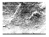
図3は、成長後のシリコン結晶膜表面のRHEEDパターンを撮影した電子線回折写真である。この写真から観察されるように、この比較例のシリコン結晶膜は、実施例1のシリコン結晶膜と異なり、回折パターンはスポット状であり、ファセットの存在を示す矢尻状のパターンも観察される。
【0024】
図4は、前記シリコン結晶膜表面のSEM写真である。このSEM写真から観察されるように、このシリコン結晶膜表面には、粒状の突起が多数存在している。
【0025】
これらの結果から、実施例1のSOI構造体において、シリコン結晶膜の結晶性および平坦性が、比較例1のSOI構造体と比べて飛躍的に向上していることが確認された。
【0026】
【発明の効果】
以上、説明したように、本発明のSOI構造体の製造方法によれば、サファイア等の絶縁性酸化物基板を用いてSOI構造体を製造する場合に、従来必要であったシリコンの固相エピタキシャル成長法などによる後処理工程を必要とせず、容易にかつ低コストで、良好なSOI構造体を製造できる。また、シリコン結晶膜の成長後の表面平坦性が非常によいことから、このSOI構造体を用いて、例えば、MOS−FET等の半導体素子を作製しようとする場合に、特性のばらつきの少ない素子を作製できる。また本発明では、基板への金属の付着とシリコン結晶膜の成長とを一貫プロセスで作製でき、界面での汚染の影響も低減することができる。
【図面の簡単な説明】
【図1】本発明によって形成されたSOI構造体表面の反射高速電子線回折パターンを撮影した電子線回折写真である。
【図2】本発明によって形成されたSOI構造体の表面の走査型電子顕微鏡写真である。
【図3】基板へのアルミニウムの付着を行わなかった比較例のSOI構造体表面の反射高速電子線回折パターンを撮影した電子線回折写真である。
【図4】基板へのアルミニウムの付着を行わなかった比較例のSOI構造体表面の走査型電子顕微鏡写真である。
【図5】γ−Al2 O3 /Si基板上にアルミニウムを付着させ、シリコンの成長温度である800℃まで昇温し、途中の段階でアルミニウムがどういう化学状態にあるかをXPSを用いて分析した結果を示すグラフである。[0001]
TECHNICAL FIELD OF THE INVENTION
The present invention relates to improvement of crystallinity and flatness of a silicon crystal film formed on an insulating substrate in an SOI (Silicon On Insulator) structure manufacturing method using an epitaxial growth method.
[0002]
[Prior art]
As a typical manufacturing method for obtaining an SOI (Silicon On Insulator) structure by epitaxially growing a silicon crystal film on an insulating substrate, a sapphire single crystal substrate is used as the insulating substrate, and a silicon crystal film is formed thereon. There is a method of growing to obtain an SOS (Silicon on Sapphire) structure. Also reported is a method of growing a γ-Al 2 O 3 layer or a magnesia spinel (MgO · Al 2 O 3 ) layer on a silicon single crystal substrate and then growing a silicon crystal film. These structures are generally manufactured by a CVD method (Chemical Vapor Deposition), an MBE method (Molecular Beam Epitaxy), or the like.
[0003]
[Problems to be solved by the invention]
However, in the conventional manufacturing method, it is not possible to obtain a silicon film with good crystallinity only by depositing silicon on an oxide substrate. After silicon deposition, the silicon film is irradiated with silicon ions to form silicon. An amorphous layer is formed, and then a post-processing step is required, such as a method of growing a solid phase epitaxial layer by annealing using the amorphous layer as a seed layer (for example, SS). Lauetal., Appl.Phys.Lett.34 (1979) 76). Further, in order to obtain a smooth surface, a post-process such as further mechanical polishing is necessary.
[0004]
Accordingly, an object of the present invention is to provide a method of manufacturing an SOI structure that can improve the crystallinity and flatness of a silicon crystal film formed on an insulating substrate in the SOI structure.
[0005]
[Means for Solving the Problems]
In order to solve the above-mentioned problems, the present inventors have made extensive studies and have obtained the following knowledge. That is, an ultrathin metal layer is formed on an oxide substrate before depositing silicon, and all the atomic bonds on the surface of the substrate are terminated with metal atoms. It was also found that when silicon is deposited on the surface having this metal atom as a terminal, the growing silicon atom and the metal atom can be lattice-matched, and a silicon growth film with good crystallinity can be obtained. The present invention has been made based on such knowledge.
[0006]
That is, the method for manufacturing an SOI structure according to the present invention is a method for manufacturing an SOI structure in which a silicon crystal film is formed on an insulating oxide substrate, wherein the metal element is grown before the silicon crystal film is grown. Is deposited on the oxide substrate with a thickness of less than 30 angstroms, and a silicon crystal film is grown on the metal element film.
[0007]
Here, the metal element is preferably at least one metal element selected from metal elements constituting the oxide substrate.
[0008]
Furthermore, it is preferable that the oxide substrate is either a single crystal Al 2 O 3 or a γ-Al 2 O 3 / Si substrate, and the metal is aluminum.
[0010]
DETAILED DESCRIPTION OF THE INVENTION
In the present invention, the insulating oxide substrate is preferably highly crystalline and single crystal. As such a material, for example, sapphire, γ-Al 2 O 3 , magnesia spinel, and zinc oxide are useful. The insulating substrate may be a substrate obtained by epitaxially growing an oxide film such as γ-Al 2 O 3 , magnesia spinel, zinc oxide, cerium oxide on a silicon substrate. Of these, sapphire substrates and γ-Al 2 O 3 / Si substrates are particularly preferable because of good insulation.
[0011]
Further, as the metal deposited on the insulating oxide substrate, the metal constituting the oxide substrate is preferable. For example, in the case of a sapphire substrate or a γ-Al 2 O 3 / Si substrate, aluminum is particularly preferable. Aluminum is useful for manufacturing SOI structures because it is a general-purpose material in semiconductor processes.
[0012]
The adhesion of the metal element to the substrate, which is a characteristic treatment in the present invention, is to terminate the irregular surface of the conventional oxide substrate surface at the atomic level with the metal element, and to change the state of the surface on which silicon is deposited. This is done to stabilize and equalize.
[0013]
As a method for growing the silicon film, a method in which a metal element attached to the surface of the substrate can be performed under a high vacuum so that the metal element is not oxidized before the start of silicon growth is preferable, for example, MBE method or UHV-CVD (Ultra High Vacuum). CVD) method.
[0014]
Further, a part of the deposited metal disappears in the process of raising the temperature of the substrate to the silicon growth temperature. The situation is shown in FIG. FIG. 5 shows the chemical state of aluminum in each stage by depositing aluminum on the γ-Al 2 O 3 / Si substrate in the MBE method and raising the temperature to 800 ° C. which is the growth temperature of silicon. It is a graph which shows the result analyzed using (X-ray Photo-electron Spectroscopy). FIG. 5 (a) shows only Al—O bonds derived from γ-Al 2 O 3 on the surface of the substrate before adhesion of aluminum. In (b), Al—O bond and Al—Al bond are detected after aluminum is deposited at room temperature. (C) is after heating up to 800 ° C. after adhesion of aluminum, Al—Al bond is not detected, and only Al—O bond is detected. That is, it can be said that aluminum has disappeared to such an extent that no Al—Al bond is detected by the heat treatment.
[0015]
Since the thickness of the metal to be deposited decreases in the course of the heat treatment, if the heat treatment conditions are different, the thickness of the metal to be deposited is changed accordingly. In other words, an appropriate film thickness exists by heat treatment, and the film quality of the silicon film is deteriorated when the film thickness is thick. For example, under the condition of heat treatment at 800 ° C. for 5 minutes, the film thickness of aluminum needs to be 30 angstroms or less.
[0016]
【Example】
Specific embodiments of the present invention are described in detail below.
[0017]
(Example 1)
First, in order to obtain an insulating oxide substrate, γ-Al 2 O 3 growth was performed on a silicon substrate. For this, a Si (111) wafer was used as a substrate. In MBE apparatus using metallic aluminum and N 2 O as raw materials, substrate temperature: 820 ° C., Knudsen cell temperature of aluminum (K-cell temperature): 1100 ° C., N 2 O pressure: 3 × 10 Single crystal γ-Al 2 O 3 was grown on the silicon substrate at −2 Pa. After growing for 60 minutes, a single crystal γ-Al 2 O 3 film having a thickness of about 50 Å was obtained.
[0018]
Next, the silicon substrate (γ-Al 2 O 3 / Si substrate) on which γ-Al 2 O 3 is grown on the surface is lowered to room temperature, and the aluminum thin film is 1 angstrom at a Knudsen cell temperature of 1050 ° C. The growth rate was 20 angstroms at a growth rate of / sec.
[0019]
Next, the substrate temperature was raised to 800 ° C., and a silicon film of about 4000 Å was grown in 5 minutes in a gas source MBE apparatus using disilane (Si 2 H 6 ) as a raw material. The above processing was continuously performed in the same MBE apparatus.
[0020]
FIG. 1 is an electron diffraction photograph taken of a reflection high-energy electron diffraction (RHEED) pattern on the surface of a grown silicon crystal film. In this photograph, a clear streak-like 7 × 7 pattern is observed, indicating that the crystallinity and flatness of the silicon crystal film are very good.
[0021]
FIG. 2 is a scanning electron microscope (SEM) photograph of the surface of the silicon crystal film. As can be observed from the photograph of FIG. 2, the surface state of the obtained silicon crystal film has few irregularities, the irregularity level is low, and the film has a flat surface.
[0022]
(Comparative Example 1)
In the same manner as in Example 1, a single crystal γ-Al 2 O 3 film was grown on a Si (111) substrate by about 50 Å. Thereafter, a silicon crystal film was grown at a substrate temperature of 800 ° C. and a silicon crystal film of about 4000 Å under the same conditions as in Example 1 without adhesion of aluminum.
[0023]
FIG. 3 is an electron diffraction photograph taken of the RHEED pattern on the surface of the grown silicon crystal film. As observed from this photograph, the silicon crystal film of this comparative example is different from the silicon crystal film of Example 1 in that the diffraction pattern is spot-like, and an arrowhead-like pattern indicating the presence of facets is also observed.
[0024]
FIG. 4 is a SEM photograph of the silicon crystal film surface. As observed from the SEM photograph, a large number of granular protrusions exist on the surface of the silicon crystal film.
[0025]
From these results, it was confirmed that in the SOI structure of Example 1, the crystallinity and flatness of the silicon crystal film were dramatically improved as compared with the SOI structure of Comparative Example 1.
[0026]
【The invention's effect】
As described above, according to the method for manufacturing an SOI structure of the present invention, when manufacturing an SOI structure using an insulating oxide substrate such as sapphire, solid phase epitaxial growth of silicon, which has been conventionally required, is performed. A good SOI structure can be manufactured easily and at low cost without the need for a post-processing step by a method or the like. In addition, since the surface flatness after the growth of the silicon crystal film is very good, an element with little variation in characteristics when a semiconductor element such as a MOS-FET is produced using this SOI structure. Can be produced. In the present invention, the adhesion of the metal to the substrate and the growth of the silicon crystal film can be produced by an integrated process, and the influence of contamination at the interface can be reduced.
[Brief description of the drawings]
FIG. 1 is an electron diffraction photograph taken of a reflection high-energy electron diffraction pattern on the surface of an SOI structure formed according to the present invention.
FIG. 2 is a scanning electron micrograph of the surface of an SOI structure formed according to the present invention.
FIG. 3 is an electron diffraction photograph obtained by photographing a reflection high-energy electron diffraction pattern on the surface of an SOI structure according to a comparative example in which aluminum was not attached to a substrate.
FIG. 4 is a scanning electron micrograph of the surface of an SOI structure of a comparative example in which aluminum was not attached to the substrate.
FIG. 5 shows that aluminum is deposited on a γ-Al 2 O 3 / Si substrate, the temperature is raised to 800 ° C., which is the growth temperature of silicon, and what chemical state the aluminum is in the middle using XPS. It is a graph which shows the result of analysis.
Claims (3)
Priority Applications (1)
| Application Number | Priority Date | Filing Date | Title |
|---|---|---|---|
| JP10976496A JP3688802B2 (en) | 1996-04-30 | 1996-04-30 | Method for manufacturing SOI structure |
Applications Claiming Priority (1)
| Application Number | Priority Date | Filing Date | Title |
|---|---|---|---|
| JP10976496A JP3688802B2 (en) | 1996-04-30 | 1996-04-30 | Method for manufacturing SOI structure |
Publications (2)
| Publication Number | Publication Date |
|---|---|
| JPH09295893A JPH09295893A (en) | 1997-11-18 |
| JP3688802B2 true JP3688802B2 (en) | 2005-08-31 |
Family
ID=14518646
Family Applications (1)
| Application Number | Title | Priority Date | Filing Date |
|---|---|---|---|
| JP10976496A Expired - Fee Related JP3688802B2 (en) | 1996-04-30 | 1996-04-30 | Method for manufacturing SOI structure |
Country Status (1)
| Country | Link |
|---|---|
| JP (1) | JP3688802B2 (en) |
Families Citing this family (1)
| Publication number | Priority date | Publication date | Assignee | Title |
|---|---|---|---|---|
| KR100707215B1 (en) * | 2006-04-25 | 2007-04-13 | 삼성전자주식회사 | Method for forming highly-orientated silicon film, method for fabricating 3d semiconductor device, and 3d semiconductor device |
-
1996
- 1996-04-30 JP JP10976496A patent/JP3688802B2/en not_active Expired - Fee Related
Also Published As
| Publication number | Publication date |
|---|---|
| JPH09295893A (en) | 1997-11-18 |
Similar Documents
| Publication | Publication Date | Title |
|---|---|---|
| JP5490271B2 (en) | Semiconductor wafer | |
| Chen et al. | Structure of CdTe (111) B grown by MBE on misoriented Si (001) | |
| US7459374B2 (en) | Method of manufacturing a semiconductor heterostructure | |
| US6313016B1 (en) | Method for producing epitaxial silicon germanium layers | |
| JP2002525255A (en) | Method for obtaining single crystal germanium layer on single crystal silicon substrate and product obtained thereby | |
| JP7290135B2 (en) | Semiconductor substrate manufacturing method and SOI wafer manufacturing method | |
| JP2007511892A (en) | Epitaxial growth of relaxed silicon germanium layers. | |
| KR100611108B1 (en) | Method of manufacturing a thin film layer | |
| JPH05217890A (en) | Crystal for producing semiconductor device and it's manufacture | |
| JPH06216131A (en) | Filling of via-hole with single crystal aluminum | |
| JP3688802B2 (en) | Method for manufacturing SOI structure | |
| JPH06232058A (en) | Preparation of epitaxial semiconductor structure | |
| JP2004051446A (en) | Oxide single crystal thin film formation method and semiconductor thin film forming method | |
| Tassis et al. | Optical and electrical characterization of high quality β-FeSi2 thin films grown by solid phase epitaxy | |
| WO2022212317A1 (en) | Method of manufacturing aluminum nitride films | |
| US5066355A (en) | Method of producing hetero structure | |
| TW201145581A (en) | Method for manufacturing epitaxial crystal substrate | |
| JP2003332242A (en) | Semiconductor substrate and its manufacturing method | |
| JP3985288B2 (en) | Semiconductor crystal growth method | |
| JP3645442B2 (en) | Silicon substrate manufacturing method | |
| Mizushima et al. | Mechanism of defect formation during low-temperature Si epitaxy on clean Si substrate | |
| JPH0256952A (en) | Method of growing caf2 film | |
| JPH05319984A (en) | Production of metallic epitaxial film | |
| JP2870061B2 (en) | Super lattice structure element | |
| JPH02220431A (en) | Formation of semiconductor substrate |
Legal Events
| Date | Code | Title | Description |
|---|---|---|---|
| A977 | Report on retrieval |
Free format text: JAPANESE INTERMEDIATE CODE: A971007 Effective date: 20041111 |
|
| A131 | Notification of reasons for refusal |
Free format text: JAPANESE INTERMEDIATE CODE: A131 Effective date: 20041126 |
|
| A521 | Written amendment |
Free format text: JAPANESE INTERMEDIATE CODE: A523 Effective date: 20050117 |
|
| A131 | Notification of reasons for refusal |
Free format text: JAPANESE INTERMEDIATE CODE: A131 Effective date: 20050318 |
|
| A521 | Written amendment |
Free format text: JAPANESE INTERMEDIATE CODE: A523 Effective date: 20050412 |
|
| TRDD | Decision of grant or rejection written | ||
| A01 | Written decision to grant a patent or to grant a registration (utility model) |
Free format text: JAPANESE INTERMEDIATE CODE: A01 Effective date: 20050520 |
|
| A61 | First payment of annual fees (during grant procedure) |
Free format text: JAPANESE INTERMEDIATE CODE: A61 Effective date: 20050609 |
|
| R150 | Certificate of patent or registration of utility model |
Free format text: JAPANESE INTERMEDIATE CODE: R150 |
|
| FPAY | Renewal fee payment (event date is renewal date of database) |
Free format text: PAYMENT UNTIL: 20080617 Year of fee payment: 3 |
|
| FPAY | Renewal fee payment (event date is renewal date of database) |
Free format text: PAYMENT UNTIL: 20090617 Year of fee payment: 4 |
|
| FPAY | Renewal fee payment (event date is renewal date of database) |
Free format text: PAYMENT UNTIL: 20090617 Year of fee payment: 4 |
|
| FPAY | Renewal fee payment (event date is renewal date of database) |
Free format text: PAYMENT UNTIL: 20100617 Year of fee payment: 5 |
|
| FPAY | Renewal fee payment (event date is renewal date of database) |
Free format text: PAYMENT UNTIL: 20100617 Year of fee payment: 5 |
|
| S531 | Written request for registration of change of domicile |
Free format text: JAPANESE INTERMEDIATE CODE: R313531 |
|
| FPAY | Renewal fee payment (event date is renewal date of database) |
Free format text: PAYMENT UNTIL: 20100617 Year of fee payment: 5 |
|
| R360 | Written notification for declining of transfer of rights |
Free format text: JAPANESE INTERMEDIATE CODE: R360 |
|
| FPAY | Renewal fee payment (event date is renewal date of database) |
Free format text: PAYMENT UNTIL: 20100617 Year of fee payment: 5 |
|
| R370 | Written measure of declining of transfer procedure |
Free format text: JAPANESE INTERMEDIATE CODE: R370 |
|
| FPAY | Renewal fee payment (event date is renewal date of database) |
Free format text: PAYMENT UNTIL: 20100617 Year of fee payment: 5 |
|
| S531 | Written request for registration of change of domicile |
Free format text: JAPANESE INTERMEDIATE CODE: R313531 |
|
| FPAY | Renewal fee payment (event date is renewal date of database) |
Free format text: PAYMENT UNTIL: 20100617 Year of fee payment: 5 |
|
| R350 | Written notification of registration of transfer |
Free format text: JAPANESE INTERMEDIATE CODE: R350 |
|
| FPAY | Renewal fee payment (event date is renewal date of database) |
Free format text: PAYMENT UNTIL: 20110617 Year of fee payment: 6 |
|
| FPAY | Renewal fee payment (event date is renewal date of database) |
Free format text: PAYMENT UNTIL: 20110617 Year of fee payment: 6 |
|
| FPAY | Renewal fee payment (event date is renewal date of database) |
Free format text: PAYMENT UNTIL: 20120617 Year of fee payment: 7 |
|
| FPAY | Renewal fee payment (event date is renewal date of database) |
Free format text: PAYMENT UNTIL: 20120617 Year of fee payment: 7 |
|
| FPAY | Renewal fee payment (event date is renewal date of database) |
Free format text: PAYMENT UNTIL: 20130617 Year of fee payment: 8 |
|
| FPAY | Renewal fee payment (event date is renewal date of database) |
Free format text: PAYMENT UNTIL: 20130617 Year of fee payment: 8 |
|
| FPAY | Renewal fee payment (event date is renewal date of database) |
Free format text: PAYMENT UNTIL: 20140617 Year of fee payment: 9 |
|
| LAPS | Cancellation because of no payment of annual fees |