JP3688697B2 - OFDM transmission method, OFDM transmitter and OFDM receiver - Google Patents
OFDM transmission method, OFDM transmitter and OFDM receiver Download PDFInfo
- Publication number
- JP3688697B2 JP3688697B2 JP2003409432A JP2003409432A JP3688697B2 JP 3688697 B2 JP3688697 B2 JP 3688697B2 JP 2003409432 A JP2003409432 A JP 2003409432A JP 2003409432 A JP2003409432 A JP 2003409432A JP 3688697 B2 JP3688697 B2 JP 3688697B2
- Authority
- JP
- Japan
- Prior art keywords
- symbol
- data
- ofdm
- circuit
- symbols
- Prior art date
- Legal status (The legal status is an assumption and is not a legal conclusion. Google has not performed a legal analysis and makes no representation as to the accuracy of the status listed.)
- Expired - Lifetime
Links
Images


Description
本発明は、等化性能を向上させるようにしたOFDM伝送方法、OFDM送信装置及びOFDM受信装置に関する。 The present invention relates to an OFDM transmission method, an OFDM transmitter, and an OFDM receiver that improve equalization performance.
近年、映像信号又は音声信号の伝送において、高品質で波数利用効率が高いディジタル変調が開発されている。特に、移動体通信においては、マルチパス干渉に強い直交周波数分割多重(以下、OFDM[orthogonal frequency division multiplex ]という)変調の採用が検討されている。更に、OFDMを用いたディジタルテレビジョン(TV)放送も研究されている。このOFDMについては、非特許文献1等に詳述されている。
In recent years, high-quality digital modulation with high wave number utilization efficiency has been developed for transmission of video signals or audio signals. In particular, in mobile communications, the adoption of orthogonal frequency division multiplex (hereinafter referred to as OFDM [orthogonal frequency division multiplex]) modulation that is resistant to multipath interference is being studied. In addition, digital television (TV) broadcasting using OFDM has been studied. This OFDM is described in detail in
OFDMは、伝送ディジタルデータを互いに直交する多数(約256乃至1024)の搬送波(以下、サブキャリアという)に分散し、夫々変調する方式である。OFDMはマルチパス干渉の影響を受けにくいという特徴の外に、周波数利用効率が高く、また、他に妨害を与えにくいという利点も有する。 OFDM is a system in which transmission digital data is distributed over a large number (approximately 256 to 1024) of carrier waves (hereinafter referred to as subcarriers) orthogonal to each other and modulated. In addition to the feature that OFDM is less susceptible to multipath interference, it has the advantage of high frequency utilization efficiency and is less likely to interfere with others.
OFDMの各サブキャリアはQPSK又は多値QAM等のシンボルデータによって変調される。この変調は逆高速フーリエ変換(以下、IFFT)回路により行われ、各サブキャリアに夫々対するN個のシンボルデータをIFFT演算することでOFDM被変調波の1シンボル(以下、OFDMシンボルともいう)が作成される。 Each subcarrier of OFDM is modulated by symbol data such as QPSK or multilevel QAM. This modulation is performed by an inverse fast Fourier transform (hereinafter referred to as IFFT) circuit, and one symbol (hereinafter also referred to as an OFDM symbol) of an OFDM modulated wave is obtained by performing an IFFT operation on N symbol data for each subcarrier. Created.
OFDMシンボルを伝送する場合には、受信側における誤り訂正を考慮して、複数のOFDMシンボルによって伝送フレームを構成し、フレーム単位で伝送路特性補正用の基準となるOFDMシンボル(以下、基準シンボルという)を挿入して伝送する。 When transmitting an OFDM symbol, a transmission frame is composed of a plurality of OFDM symbols in consideration of error correction on the receiving side, and an OFDM symbol (hereinafter referred to as a reference symbol) that serves as a reference for correcting transmission path characteristics in units of frames. ) Is inserted and transmitted.
図8はこのフレーム単位の伝送方式を説明するための説明図であり、非特許文献2に記載されたものである。
FIG. 8 is an explanatory diagram for explaining the transmission method in units of frames, and is described in Non-Patent
図8に示すように、OFDMの伝送フレームは周波数方向(キャリア単位)及び時間方向(OFDMシンボル単位)の組みのデータによって構成される。フレームの各時間スロットは各OFDMシンボルを示している。1OFDMシンボルのサブキャリア数は448であり、1フレームのOFDMシンボル数は300である。なお、サブキャリアの数は使用するIFFT回路のポイント数によって決定される。図8では、1フレームは周波数方向に448個で、時間方向に300個のデータによって構成される。 As shown in FIG. 8, an OFDM transmission frame is composed of a set of data in the frequency direction (carrier unit) and the time direction (OFDM symbol unit). Each time slot of the frame represents each OFDM symbol. The number of subcarriers in one OFDM symbol is 448, and the number of OFDM symbols in one frame is 300. Note that the number of subcarriers is determined by the number of points in the IFFT circuit to be used. In FIG. 8, one frame is composed of 448 data in the frequency direction and 300 data in the time direction.
フレームの1番目の時間スロットのOFDMシンボルは受信同期用のヌルシンボルであり、448個の全サブキャリアが振幅0のシンボルデータによって変調されて作成される。2番目の時間スロットは各サブキャリアの位相基準となる基準シンボルであり、3番目の時間スロットのOFDMシンボルは伝送制御用の固定データである。4番目以降の時間スロットのOFDMシンボル(情報シンボル)によって情報シンボルデータが伝送される。 The OFDM symbol in the first time slot of the frame is a null symbol for reception synchronization, and is created by modulating all 448 subcarriers with symbol data having an amplitude of 0. The second time slot is a reference symbol serving as a phase reference for each subcarrier, and the OFDM symbol in the third time slot is fixed data for transmission control. Information symbol data is transmitted by OFDM symbols (information symbols) in the fourth and subsequent time slots.
なお、情報シンボルデータについては周波数方向及び時間方向でインターリーブを行うことがある。インターリーブによって、特定の周波数スロット及び時間スロットが妨害を受けた場合でも連続的なデータの誤りを防止することができ、受信側における誤り訂正により、データを復元することができる可能性が高くなる。 Information symbol data may be interleaved in the frequency direction and the time direction. Interleaving can prevent continuous data errors even when specific frequency slots and time slots are disturbed, and increases the possibility that data can be restored by error correction on the receiving side.
次に、OFDMの等化技術について説明する。 Next, an OFDM equalization technique will be described.
OFDM伝送においては、マルチパスによる符号間干渉を防止するためにガード期間が設けられている。図9はOFDM信号のガード期間を説明するための説明図である。図9においては、説明を簡略化するために1つのサブキャリアによるOFDM信号を示してある。 In OFDM transmission, a guard period is provided to prevent intersymbol interference due to multipath. FIG. 9 is an explanatory diagram for explaining a guard period of an OFDM signal. In FIG. 9, an OFDM signal with one subcarrier is shown to simplify the description.
図9に示すように、OFDMの1シンボルの信号は、ガード期間と有効シンボル期間とによって構成される。ガード期間は有効シンボル期間の後半の信号が巡回的に複写されて形成される。マルチパス干渉の遅延時間がガード期間以内である場合には、復調時において有効シンボル期間の信号のみを復調することで、遅延した隣接シンボルによる符号間干渉を防止することができる。 As shown in FIG. 9, a signal of one symbol of OFDM is composed of a guard period and an effective symbol period. The guard period is formed by cyclically copying the signal in the latter half of the effective symbol period. When the delay time of multipath interference is within the guard period, it is possible to prevent intersymbol interference due to delayed adjacent symbols by demodulating only the signal in the effective symbol period at the time of demodulation.
図10はこのようなガード期間による等化を説明するための説明図である。 FIG. 10 is an explanatory diagram for explaining equalization by such a guard period.
いま、図10(a)に示すOFDMシンボルの直接波の信号波形に対して、マルチパス干渉波の信号波形の遅延時間が図10(b)に示すようにガード期間内であるものとする。受信側では図10(a)のOFDMシンボルと図10(b)の干渉波との和信号が得られる(図10(c))。この場合には、干渉波の遅延時間がガード期間以内であるので、有効シンボル期間における受信信号(和信号)は、OFDMシンボルと同一周波数で位相及び振幅が変化したものとなる。即ち、図10(a)のOFDMシンボルが例えば図11のシンボルデータS0 によって変調されたものである場合には、受信信号を復調すると、例えば図11のシンボルデータS1 が得られることを示している。 Now, it is assumed that the delay time of the signal waveform of the multipath interference wave is within the guard period as shown in FIG. 10B with respect to the signal waveform of the direct wave of the OFDM symbol shown in FIG. On the receiving side, a sum signal of the OFDM symbol of FIG. 10A and the interference wave of FIG. 10B is obtained (FIG. 10C). In this case, since the delay time of the interference wave is within the guard period, the received signal (sum signal) in the effective symbol period has a phase and amplitude changed at the same frequency as the OFDM symbol. That is, when the OFDM symbol of FIG. 10 (a) is, for example, modulated by the symbol data S0 of FIG. 11, demodulating the received signal, for example, can obtain the symbol data S1 of FIG. .
即ち、予め位相及び振幅が既知の基準シンボルを復調し、元のシンボルデータと復調シンボルデータとの位相及び振幅の変化分(オフセット)を相殺するように、復調シンボルデータを補正することにより、マルチパス干渉の影響を受けないデータ伝送が可能となる。なお、マルチパス干渉の影響は各サブキャリア毎に相違するので、基準シンボルは各サブキャリア毎に設定されている。なお、サブキャリア毎に補正のための係数を切換えることにより、オフセットの補正は1個の複素乗算器によって実現することができる。 That is, by demodulating a reference symbol whose phase and amplitude are known in advance and correcting the demodulated symbol data so as to cancel out the change (offset) of the phase and amplitude between the original symbol data and the demodulated symbol data, Data transmission that is not affected by path interference is possible. Since the influence of multipath interference differs for each subcarrier, the reference symbol is set for each subcarrier. Note that the offset correction can be realized by one complex multiplier by switching the correction coefficient for each subcarrier.
しかし、受信状態によっては遅延時間がガード期間を越えるようなマルチパスが存在することが考えられる。マルチパスの遅延時間がガード期間を越えると、基準シンボルを用いても復調シンボルを等化することができない。図12はこの問題点を説明するための説明図である。 However, depending on the reception state, there may be a multipath whose delay time exceeds the guard period. If the multipath delay time exceeds the guard period, the demodulated symbols cannot be equalized even if the reference symbols are used. FIG. 12 is an explanatory diagram for explaining this problem.
図12(a),(b)に示すように、マルチパス干渉波の遅延時間がガード期間を越えると、所定のOFDMシンボルの有効シンボル期間に隣接した前OFDMシンボルの後半の部分がマルチパスとして加えられ、復調出力に符号間干渉がが生じる。従って、基準シンボルを用いてもマルチパスを完全に除去することはできない。更に、マルチパスの遅延時間がガード期間を越えた場合には、等化用の基準シンボルも符号間干渉によって劣化することから、等化後の復調シンボルの劣化が大きくなってしまう。基準シンボルは1フレームに1回しか伝送されないので、基準シンボルが妨害を受けた場合には復調信号が極めて劣化してしまうという問題があった。 As shown in FIGS. 12A and 12B, when the delay time of the multipath interference wave exceeds the guard period, the latter half of the previous OFDM symbol adjacent to the effective symbol period of the predetermined OFDM symbol becomes a multipath. In addition, intersymbol interference occurs in the demodulated output. Therefore, even if the reference symbol is used, the multipath cannot be completely removed. Furthermore, when the multipath delay time exceeds the guard period, the reference symbol for equalization also deteriorates due to the intersymbol interference, so that the deterioration of the demodulated symbol after equalization becomes large. Since the reference symbol is transmitted only once per frame, there is a problem that the demodulated signal is extremely deteriorated when the reference symbol is disturbed.
なお、ガード期間を長く設定することにより等化範囲を拡大することができるが、伝送レートが低下してしまうという欠点がある。なお、図12の例では、1シンボル期間を80μ秒とすると、ガード期間は16μ秒に設定されている。
このように、従来、ガード期間を越える遅延時間のマルチパスが発生した場合には、復調信号の劣化が著しいという問題点があった。 Thus, conventionally, when a multipath having a delay time exceeding the guard period occurs, there is a problem that the demodulated signal is significantly deteriorated.
本発明はかかる問題点に鑑みてなされたものであって、OFDMの伝送フレーム中に2シンボル以上波形を連続させて基準シンボルを伝送することにより、等化後の復調シンボルの劣化及び基準シンボルが妨害を受けた場合の悪影響を抑制することができるOFDM伝送方法、OFDM送信装置及びOFDM受信装置を提供することを目的とする。 The present invention has been made in view of such a problem. By transmitting a reference symbol with a waveform of two or more symbols continuous in an OFDM transmission frame, degradation of demodulated symbols after equalization and reference symbols are reduced. An object of the present invention is to provide an OFDM transmission method, an OFDM transmission apparatus, and an OFDM reception apparatus that can suppress adverse effects caused by interference.
本発明の請求項1に係るOFDM送信装置は、受信同期用のシンボルデータ、基準データ及び情報シンボルデータに基づく伝送フレームを構成するように、前記受信同期用のシンボルデータ、基準データ及び情報シンボルデータのデータ配列を行う配列手段と、この配列手段からのデータによって複数のサブキャリアを直交周波数分割多重変調することにより、受信同期用の同期シンボル、基準シンボル及び情報シンボルによって構成される伝送フレームを作成する変調手段とを具備し、前記基準シンボルは、波形が連続した2つの基準シンボルによって等価的に1基準シンボルとして前記伝送フレーム中に配列されることを特徴とするものであり、
本発明の請求項2に係るOFDM伝送方法は、受信同期用のシンボルデータ、基準データ及び情報シンボルデータに基づく伝送フレームを構成するように、前記受信同期用のシンボルデータ、基準データ及び情報シンボルデータのデータ配列を行う配列手順と、この配列手順によって配列されたデータによって複数のサブキャリアを直交周波数分割多重変調することにより、受信同期用の同期シンボル、基準シンボル及び情報シンボルによって構成される伝送フレームを作成する変調手順とを具備し、前記基準シンボルは、波形が連続した2つの基準シンボルによって等価的に1基準シンボルとして前記伝送フレーム中に配列することを特徴とするものであり、
本発明の請求項3に係るOFDM受信装置は、受信同期用のシンボルデータ、基準データ及び情報シンボルデータに対する複数のサブキャリアを用いた直交周波数分割多重変調によって、受信同期用の同期シンボル、波形が連続した2つの基準シンボルによって等価的に1基準シンボルとして配列される基準シンボル及び情報シンボルによって構成される伝送フレームが作成されて伝送され、この伝送フレームを直交周波数分割多重復調して情報シンボルデータ及び基準データを得る復調手段と、前記復調手段の復調出力のうち、前記2以上連続した基準シンボルに対する復調出力を用いて前記各サブキャリアの振幅及び位相ずれを検出する検出手段と、この検出手段の検出結果に基づいて前記情報シンボルデータの振幅及び位相ずれを補正する補正手段とを具備したことを特徴とするものである。
The OFDM transmitter according to
In the OFDM transmission method according to
In the OFDM receiver according to
本発明においては、隣接する基準シンボル間で波形を連続させながら1伝送フレーム中で2以上の基準シンボルを連続させて伝送することにより、伝送フレーム中に、等価的に期間が長い1基順シンポルを配列することになる。これにより、遅延時間が長いマルチパスが発生した場合でも、受信側における等化性能を向上させることができ、復調シンボルの劣化が抑制される。 In the present invention, two or more reference symbols are continuously transmitted in one transmission frame while a waveform is continuous between adjacent reference symbols. Will be arranged. Thereby, even when a multipath having a long delay time occurs, the equalization performance on the reception side can be improved, and the deterioration of the demodulated symbol is suppressed.
以上説明したように本発明によれば、OFDMの伝送フレーム中に2シンボル以上波形を連続させて基準シンボルを伝送することにより、等化後の復調シンボルの劣化及び基準シンボルが妨害を受けた場合の悪影響を抑制することができるという効果を有する。 As described above, according to the present invention, when a reference symbol is transmitted by continuing a waveform of two or more symbols in an OFDM transmission frame, the demodulated symbol deteriorates after equalization and the reference symbol is disturbed. It has the effect that the adverse effect of can be suppressed.
以下、図面を参照して本発明の実施例について説明する。図1は本発明に係るOFDM伝送方法の一実施例を示す説明図である。なお、図1では、1乃至Mの各時間スロットは各OFDMシンボルを示している。 Embodiments of the present invention will be described below with reference to the drawings. FIG. 1 is an explanatory view showing an embodiment of the OFDM transmission method according to the present invention. In FIG. 1, each time slot from 1 to M indicates each OFDM symbol.
1OFDMシンボルのサブキャリア数はNである。OFDMの伝送フレームはM個のOFDMシンボルによって構成される。即ち、1伝送フレームは、周波数方向にN個で時間方向にM個のデータによって構成される。 The number of subcarriers in one OFDM symbol is N. An OFDM transmission frame is composed of M OFDM symbols. That is, one transmission frame is composed of N data in the frequency direction and M data in the time direction.
図1に示すように、伝送フレームの先頭の時間スロットは受信同期用のヌルシンボルであり、全サブキャリアに振幅0のシンボルデータが割当てられる。本実施例においては、第2及び第3番目の時間スロットは、各サブキャリアの等化基準信号として基準シンボルA、基準シンボルBが割当てられている。4番目の時間スロット以降は情報シンボルが割当てられている。 As shown in FIG. 1, the first time slot of a transmission frame is a null symbol for reception synchronization, and symbol data having an amplitude of 0 is assigned to all subcarriers. In the present embodiment, the reference symbol A and the reference symbol B are allocated to the second and third time slots as equalization reference signals for each subcarrier. Information symbols are assigned after the fourth time slot.
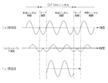
図2は図1中の基準シンボルA,Bの具体的な伝送方法を示す説明図である。なお、図2では、説明を簡略化するために、1つのサブキャリアのみの波形を示している。 FIG. 2 is an explanatory diagram showing a specific method for transmitting the reference symbols A and B in FIG. In FIG. 2, for simplicity of explanation, only one subcarrier waveform is shown.
基準シンボルAはガード期間G1 及び有効シンボル期間R1 を有している。ガード期間G1 は有効シンボル期間R1 の後半部分の波形が複写されたものである。また、基準シンボルBはガード期間G2 及び有効シンボル期間R2 を有している。ガード期間G2 は有効シンボル期間R2 の後半部分の波形が複写されたものである。本実施例においては、図2に示すように、基準シンボルAの終端の波形に基準シンボルBの波形が連続するように、有効シンボル期間R1 、R2 の波形の振幅及び位相を設定するようになっている。これにより、これらの2つの基準シンボルA,Bは、等価的にガード期間が長くなった1つの基準シンボルとみなすことができる。 The reference symbol A has a guard period G1 and an effective symbol period R1. The guard period G1 is a copy of the waveform of the latter half of the effective symbol period R1. The reference symbol B has a guard period G2 and an effective symbol period R2. The guard period G2 is a copy of the waveform of the latter half of the effective symbol period R2. In the present embodiment, as shown in FIG. 2, the amplitude and phase of the waveforms of the effective symbol periods R1 and R2 are set so that the waveform of the reference symbol B continues to the waveform of the end of the reference symbol A. ing. Thus, these two reference symbols A and B can be regarded as one reference symbol having an equivalently longer guard period.
ところで、各サブキャリアは直交条件を満足しているので、各サブキャリアの波数は有効シンボル期間において整数となる。例えば、図2に示すサブキャリアは、有効シンボル期間の波数が2であることが示されている。従って、基準シンボルBを基準シンボルAに連続させるためには、ガード期間の長さに対応する位相だけ基準シンボルA,Bの開始位相をずらせばよい。例えば、図2では、ガード期間G1 ,G2 の長さが有効シンボル期間R1 ,R2 の1/4であるので、基準シンボルA,Bの相互の開始位相を180度ずらせばよい。 By the way, since each subcarrier satisfies the orthogonality condition, the wave number of each subcarrier becomes an integer in the effective symbol period. For example, the subcarrier shown in FIG. 2 indicates that the wave number of the effective symbol period is 2. Therefore, in order to make the reference symbol B continue to the reference symbol A, it is only necessary to shift the start phases of the reference symbols A and B by the phase corresponding to the length of the guard period. For example, in FIG. 2, since the lengths of the guard periods G1 and G2 are 1/4 of the effective symbol periods R1 and R2, the start phases of the reference symbols A and B may be shifted by 180 degrees.
いま、図3に示すように、OFDMシンボルのN本のサブキャリアのキャリア番号kを周波数順に−N/2〜0〜(N/2)−1とする。また、有効シンボル期間の長さを1とした場合におけるガード期間の長さをxとする。そうすると、k番目のサブキャリアにおけるガード期間分の位相差Δθk は下記(1)式によって表わされる。 Now, as shown in FIG. 3, the carrier numbers k of the N subcarriers of the OFDM symbol are set to −N / 2 to 0 to (N / 2) −1 in order of frequency. Further, the length of the guard period when the length of the effective symbol period is 1 is assumed to be x. Then, the phase difference Δθk for the guard period in the kth subcarrier is expressed by the following equation (1).
Δθk =x・k・2π …(1)
k番目のキャリアにおける基準シンボルA,Bの位相を夫々θ1k,θ2kとすると、2つの基準シンボルA,Bを連続させるためには、下記(2)式を満足する必要がある。
Δθk = x · k · 2π (1)
When the phases of the reference symbols A and B in the k-th carrier are θ1k and θ2k, respectively, in order to make the two reference symbols A and B continuous, it is necessary to satisfy the following equation (2).
θ1k=θ2k−Δθk
=θ2k−x・k・2π …(2)
なお、基準シンボルA,Bの振幅は等しくする。
θ1k = θ2k−Δθk
= Θ2k−x · k · 2π (2)
The amplitudes of the reference symbols A and B are made equal.
例えば、図4では、有効シンボル期間の波数が1のサブキャリアについて示してある。即ち、k=1である。また、ガード期間の間隔は有効シンボル期間の1/4に設定されている。従って、これらの条件を上記(2)式に代入すると、下記(3)式が得られる。 For example, FIG. 4 shows a subcarrier having a wave number of 1 in the effective symbol period. That is, k = 1. In addition, the interval of the guard period is set to 1/4 of the effective symbol period. Therefore, when these conditions are substituted into the above equation (2), the following equation (3) is obtained.
θ1k=θ2k−1/4・1・2π
=θ2k−π/2 …(3)
この(3)式から明らかなように、この場合には、基準シンボルBの位相を基準シンボルAよりも90度だけ進めればよい(図4参照)。
θ1k = θ2k-1 / 4 ・ 1 ・ 2π
= Θ2k−π / 2 (3)
As is apparent from the equation (3), in this case, the phase of the reference symbol B may be advanced by 90 degrees with respect to the reference symbol A (see FIG. 4).
次に、本実施例のOFDM伝送方法の作用について説明する。 Next, the operation of the OFDM transmission method of this embodiment will be described.
1OFDMシンボルはN本のサブキャリアを有している。各サブキャリアは例えば0シンボルデータ、所定の基準データ又は情報シンボルデータによって変調される。M個のOFDMシンボルによって伝送フレームを構成する。0シンボルデータで変調されたOFDMシンボル(ヌルシンボル)は伝送フレームの先頭の時間スロットにおいて伝送される。各時間スロットはガード期間及び有効シンボル期間によって構成されており、ガード期間の波形は有効シンボル期間の後半の波形が複写されたものである。 One OFDM symbol has N subcarriers. Each subcarrier is modulated by, for example, 0 symbol data, predetermined reference data, or information symbol data. A transmission frame is composed of M OFDM symbols. An OFDM symbol (null symbol) modulated with 0 symbol data is transmitted in the first time slot of the transmission frame. Each time slot is composed of a guard period and an effective symbol period, and the waveform of the guard period is a copy of the latter half of the effective symbol period.
次の2番目の時間スロットでは、サブキャリアが所定の基準データによって変調された基準シンボルAが伝送される。次の3番目の時間スロットにおいては、基準シンボルBが伝送される。基準シンボルBの位相は基準シンボルAの位相に対して上記(3)式を満足する。これにより、各サブキャリア毎に、基準シンボルAのガード期間G1 及び有効シンボル期間R1 の波形に連続して基準シンボルBのガード期間G2 及び有効シンボル期間R2 の波形が伝送される。即ち、基準シンボルBのガード期間が等価的にガード期間G1 +有効シンボル期間R1 +ガード期間G2 だけ長くなったことに相当する。4乃至M番目の時間スロットでは、情報シンボルデータによって変調された情報シンボルが伝送される。 In the next second time slot, a reference symbol A in which a subcarrier is modulated by predetermined reference data is transmitted. In the next third time slot, the reference symbol B is transmitted. The phase of the reference symbol B satisfies the above expression (3) with respect to the phase of the reference symbol A. As a result, the waveforms of the guard period G2 and effective symbol period R2 of the reference symbol B are transmitted in succession to the waveforms of the guard period G1 and effective symbol period R1 of the reference symbol A for each subcarrier. That is, the guard period of the reference symbol B is equivalently increased by the guard period G1 + the effective symbol period R1 + the guard period G2. In the 4th to Mth time slots, information symbols modulated by the information symbol data are transmitted.
いま、マルチパス干渉波の遅延時間がガード期間よりも長いものとする。しかし、この場合でも、遅延時間がガード期間G1 +有効シンボル期間R1 +ガード期間G2 よりも短い場合には、基準シンボルBの有効シンボル期間R2 におけるマルチパス干渉波は、有効シンボル期間R2 と同一波形となる。従って、この場合の受信波は、基準シンボルBと同一周波数で位相及び振幅が変化したものとなる。基準シンボルBの位相及び振幅は既知であるので、復調信号を変化分だけ補正することによって、マルチパスの影響を受けない基準データを再生することができる。 Assume that the delay time of the multipath interference wave is longer than the guard period. However, even in this case, if the delay time is shorter than the guard period G1 + the effective symbol period R1 + the guard period G2, the multipath interference wave in the effective symbol period R2 of the reference symbol B has the same waveform as the effective symbol period R2. It becomes. Accordingly, the received wave in this case has a phase and amplitude that are changed at the same frequency as that of the reference symbol B. Since the phase and amplitude of the reference symbol B are known, it is possible to reproduce reference data that is not affected by multipath by correcting the demodulated signal by the amount of change.
次に、復調した基準データを用いて、情報シンボルの復調シンボルを各サブキャリア毎に等化する。基準信号がマルチパスの影響を受けていないので、復調シンボルの劣化を抑制することができる。 Next, the demodulated reference data is used to equalize demodulated symbols of information symbols for each subcarrier. Since the reference signal is not affected by multipath, it is possible to suppress the deterioration of the demodulated symbol.
このように、本実施例においては、連続した2つの時間スロットにおいて基準シンボルを伝送すると共に、これらの基準シンボルの位相及び振幅を調整することにより、2つの基準シンボルが連続するように設定しており、等価的にガード期間を十分に延長することができる。このため、基準シンボルについてはマルチパスの影響を受けない復調が可能であり、マルチパスによる復調シンボルの劣化を抑制することができる。 Thus, in this embodiment, the reference symbols are transmitted in two consecutive time slots, and the two reference symbols are set to be continuous by adjusting the phase and amplitude of these reference symbols. Equivalently, the guard period can be sufficiently extended. Therefore, the reference symbol can be demodulated without being affected by multipath, and deterioration of the demodulated symbol due to multipath can be suppressed.
なお、基準シンボルAのガード期間として基準シンボルBのガード期間G2 及び有効シンボル期間R2 を用いることができるので、前ゴーストにも対応することができるという利点もある。 Since the guard period G2 and the effective symbol period R2 of the reference symbol B can be used as the guard period of the reference symbol A, there is an advantage that it is possible to cope with the previous ghost.
図5は本発明に係るOFDM送信装置の一実施例を示すブロック図である。 FIG. 5 is a block diagram showing an embodiment of the OFDM transmitter according to the present invention.
入力端子1を介して入力された2ビットの情報データはS/P変換回路2に与えられる。S/P変換回路2はシリアルデータをパラレルデータに変換してシンボルマッピング回路3に与える。シンボルマッピング回路3は、例えばPSK変調又はQAM変調等によって、情報データを情報シンボルデータ(Iデータ,Qデータ)に変換する。シンボルマッピング回路3からの情報シンボルデータはマルチプレクス回路4に与えられる。
2-bit information data input via the
マルチプレクス回路4にはROM5,6,7の出力も与えられるようになっている。ROM5,6,7には夫々0シンボルデータ、基準データA及び基準データBが格納されている。なお、基準データA,Bはこれらの基準データA,Bに基づいて作成されたOFDMシンボル(基準シンボルA,B)の波形が連続するように、値が設定されている。マルチプレクス回路4はシンボルマッピング回路3の出力及びROM5乃至7の出力を伝送フレームの各時間スロットに対応して選択してインターリーブ回路8に出力する。インターリーブ回路8は、入力されたデータをインターリーブさせてIFFT回路9に出力する。
The
IFFT回路9は入力されたN個のデータを用いてIFFT処理することにより、OFDM被変調波(OFDMシンボル)を作成してガード期間付加回路10に出力する。
The IFFT circuit 9 performs an IFFT process using the input N pieces of data, thereby creating an OFDM modulated wave (OFDM symbol) and outputting it to the guard
ガード期間付加回路10はマルチパスの影響を低減するために、OFDM被変調波にガード期間を付加し、I軸,Q軸の信号を夫々D/A変換器11,12に出力する。D/A変換器11,12は入力されたディジタル信号をアナログ信号に変換してローパスフィルタ(以下、LPFという)13,14に出力する。LPF13,14は夫々入力信号出力の高調波成分を除去して直交変調回路15の乗算器18,19に出力する。
The guard
直交変調回路15は、局部発振器16、移相器17、乗算器18、19及び加算器20によって構成されている。局部発振器16は所定周波数のキャリアを発生して移相器17に出力すると共に、乗算器18に同相軸キャリアとして出力する。移相器17は局部発振器16の発振出力を90度移相させて直交軸キャリアを作成して乗算器19に出力する。乗算器18はLPF13の出力と同相軸キャリアとの乗算によって同相軸変調出力を得て加算器20に出力する。乗算器19はLPF14の出力と直交軸キャリアとの乗算によって直交軸変調出力を得て加算器20に出力する。加算器20は乗算器18,19の出力を加算して、直交変調出力を周波数変換回路21に出力する。 The quadrature modulation circuit 15 includes a local oscillator 16, a phase shifter 17, multipliers 18 and 19, and an adder 20. The local oscillator 16 generates a carrier having a predetermined frequency and outputs it to the phase shifter 17 and outputs it to the multiplier 18 as an in-phase axis carrier. The phase shifter 17 shifts the oscillation output of the local oscillator 16 by 90 degrees to create an orthogonal axis carrier and outputs it to the multiplier 19. The multiplier 18 obtains an in-phase axis modulation output by multiplication of the output of the LPF 13 and the in-phase axis carrier, and outputs it to the adder 20. The multiplier 19 obtains an orthogonal axis modulation output by multiplication of the output of the LPF 14 and the orthogonal axis carrier, and outputs it to the adder 20. The adder 20 adds the outputs of the multipliers 18 and 19 and outputs an orthogonal modulation output to the frequency conversion circuit 21.
周波数変換回路21はバンドパスフィルタ(以下、BPFという)22、増幅器23、乗算器24、局部発振器25及びBPF26によって構成されている。直交変調出力はBPF22に与えられ、BPF22は直交変調出力を帯域制限して増幅器23を介して乗算器24に与える。局部発振器22は中間周波数帯に周波数変換するための所定周波数の局部発振出力を乗算器24に与える。乗算器24は増幅器23の出力と局部発振出力との乗算によってOFDM被変調波の直交変調出力を高周波数帯に変換してBPF26に出力する。BPF26は乗算器24の出力を帯域制限してRF信号として出力する。
The frequency conversion circuit 21 includes a band-pass filter (hereinafter referred to as BPF) 22, an
なお、入力端子27を介してタイミング回路28にクロックが供給されるようになっている。タイミング回路28は、入力されたクロックに基づいて、所定周波数のクロックを発生すると共に、各種タイミング信号を発生して各回路に供給する。 Note that a clock is supplied to the timing circuit 28 via the input terminal 27. The timing circuit 28 generates a clock having a predetermined frequency based on the input clock, and generates various timing signals and supplies them to each circuit.
次に、このように構成された実施例の動作について説明する。 Next, the operation of the embodiment configured as described above will be described.
入力端子1を介して入力された情報データはS/P変換器2によってパラレルデータに変換された後、シンボルマッピング回路3によってIデータ及びQデータから成る情報シンボルデータに変換される。シンボルマッピング回路3からの情報シンボルデータはマルチプレクス回路4に供給される。マルチプレクス回路4にはROM5,6,7から夫々0シンボルデータ、基準データA及び基準データBも入力されており、マルチプレクス回路4は、図1の伝送フレームの各時間スロットに対応させて情報シンボルデータ、0シンボルデータ及び基準データA,Bを切換えてインターリーブ回路8に与える。インターリーブ回路8は入力されたデータをインターリーブした後IFFT回路9に出力する。
The information data input through the
なお、入力端子27にはクロックが入力されており、タイミング回路28はこのクロックに基づいて所定周波数のクロック及び各種タイミング信号を発生して各回路に供給している。 Note that a clock is input to the input terminal 27, and the timing circuit 28 generates a clock having a predetermined frequency and various timing signals based on this clock and supplies them to each circuit.
IFFT回路9は、入力されたN個のシンボルを用いてIFFT演算を行う。これにより、N個のシンボルに対するOFDM変調が行われて、OFDM被変調波の実部Re及び虚部Imがガード期間付加回路10に出力される。
The IFFT circuit 9 performs an IFFT operation using the input N symbols. As a result, OFDM modulation is performed on the N symbols, and the real part Re and the imaginary part Im of the OFDM modulated wave are output to the guard
マルチプレクス回路4がROM5を選択することにより、IFFT回路9からはヌルシンボルが出力される。また、マルチプレクス回路4がROM6,7を選択することにより、夫々基準シンボルA,BがIFFT回路9から出力される。同様に、マルチプレクス回路4がシンボルマッピング回路3の出力を選択することにより、情報シンボルが得られる。マルチプレクス回路4が図1の伝送フレームの時間スロットに対応して選択を行うことにより、IFFT回路9からは図1に示す伝送フレームが出力される。
When the
ガード期間付加回路10は入力されたOFDM被変調波の実部Re及び虚部Imに夫々マルチパスの影響を低減するためのガード期間を付加して、D/A変換器11,12に出力する。基準データA,Bは、サブキャリア周波数及びガード期間の長さに基づいて設定されており、基準シンボルAのガード期間及び有効シンボル期間の波形に連続して基準シンボルBのガード期間及び有功シンボル期間の波形が続く。
The guard
D/A変換器11,12は入力された信号をアナログ信号に変換して夫々LPF13,14に与え、LPF13,14はOFDMシンボルを帯域制限して夫々直交変調回路15の乗算器18、19に出力する。局部発振器16は所定周波数のキャリアを発生しており、移相器17はこのキャリアを90度移相させる。局部発振器16からの発振出力は同相軸キャリアとして乗算器18に供給され、乗算器18は同相軸キャリアとLPF13の出力との乗算によって同相軸変調出力を得て加算器20に出力する。乗算器19は移相器17からの直交軸キャリアとLPF14の出力との乗算によって直交軸変調出力を得て加算器20に出力する。乗算器18、19の出力は加算器20によって加算されて直交変調出力が得られる。 The D / A converters 11 and 12 convert the input signals into analog signals and apply them to the LPFs 13 and 14, respectively. The LPFs 13 and 14 band-limit the OFDM symbols to the multipliers 18 and 19 of the orthogonal modulation circuit 15, respectively. Output. The local oscillator 16 generates a carrier having a predetermined frequency, and the phase shifter 17 shifts the carrier by 90 degrees. The oscillation output from the local oscillator 16 is supplied to the multiplier 18 as an in-phase axis carrier, and the multiplier 18 obtains an in-phase axis modulation output by multiplication of the in-phase axis carrier and the output of the LPF 13 and outputs it to the adder 20. The multiplier 19 obtains an orthogonal axis modulation output by multiplication of the orthogonal axis carrier from the phase shifter 17 and the output of the LPF 14 and outputs it to the adder 20. The outputs of the multipliers 18 and 19 are added by an adder 20 to obtain an orthogonal modulation output.
直交変調回路15の直交変調出力は、周波数変換回路21のBPF22によって帯域制限された後、増幅器23によって増幅されて乗算器24に与えられる。乗算器24には局部発振器25から局部発振出力が与えられており、乗算器24は直交変調出力を高周波数(RF)帯の信号に周波数変換する。乗算器24の出力はBPF26によって帯域制限されてRF信号として出力される。
The quadrature modulation output of the quadrature modulation circuit 15 is band-limited by the BPF 22 of the frequency conversion circuit 21, amplified by the
このように、本実施例においては、伝送フレームを構成する場合に、2番目の時間スロットで基準シンボルAを伝送し、次いで3番目の時間スロットで基準シンボルBを伝送するようにしている。基準シンボルA,Bの各サブキャリアを変調する基準データA,Bは、各サブキャリア周波数及びガード期間付加回路10によるガード期間の長さに基づいて設定されており、基準シンボルA,Bは各サブキャリア毎に波形が連続する。
Thus, in this embodiment, when a transmission frame is configured, the reference symbol A is transmitted in the second time slot, and then the reference symbol B is transmitted in the third time slot. The reference data A and B for modulating the subcarriers of the reference symbols A and B are set based on the subcarrier frequency and the length of the guard period by the guard
図6は本発明に係るOFDM受信装置の一実施例を示すブロック図である。 FIG. 6 is a block diagram showing an embodiment of the OFDM receiving apparatus according to the present invention.
入力端子31にはN本のサブキャリアを有するOFDM被変調波(OFDMシンボル)が伝送フレーム単位で入力される。伝送フレームの先頭の時間スロットではヌルシンボルが伝送され、2番目の時間スロットでは基準シンボルAが伝送され、3番目の時間スロットでは基準シンボルBが伝送される。4乃至M番目の時間スロットにおいて情報シンボルが伝送されるようになっている。また、基準シンボルA,Bは連続した波形となっている。これらのOFDMシンボルは、所定のキャリア周波数で直交変調された後にRF帯に周波数変換されて入力されるようになっている。 An OFDM modulated wave (OFDM symbol) having N subcarriers is input to the input terminal 31 in units of transmission frames. A null symbol is transmitted in the first time slot of the transmission frame, a reference symbol A is transmitted in the second time slot, and a reference symbol B is transmitted in the third time slot. Information symbols are transmitted in the 4th to Mth time slots. The reference symbols A and B have a continuous waveform. These OFDM symbols are subjected to orthogonal modulation at a predetermined carrier frequency and then frequency-converted to an RF band and input.
このRF帯のOFDMシンボルはBPF32に供給される。BPF32は帯域外の雑音を除去して増幅器33に出力する。増幅器33はBPF32の出力を増幅して乗算器34に出力する。局部発振器35はRF帯の信号を周波数変換するための局部発振出力を乗算器34に出力する。乗算器34は増幅器33の出力と局部発振出力との乗算によってOFDM被変調波を所定の周波数に周波数変換してBPF36に出力する。BPF36はOFDMシンボルの高調波成分を除去して利得可変増幅器37に出力する。
This OFDM symbol in the RF band is supplied to the
利得可変増幅器37は後述するエンベロープ検出回路50に制御されて、BPF36の出力を一定振幅に変換して直交検波回路38に出力する。直交検波回路38は乗算器39,40、局部発振器41及び移相器42によって構成されている。局部発振器41は後述するキャリア再生回路43に制御されて、所定周波数の再生キャリアを発生して乗算器39及び移相器42に出力するようになっている。局部発振器41の出力は同相軸キャリアとして乗算器39に供給される。移相器42は局部発振出力を90度移相して直交軸キャリアを再生して乗算器40に与える。乗算器39は可変利得増幅器37の出力に同相軸キャリアを乗算して同相軸検波出力を得、乗算器40は可変利得増幅器37の出力に直交軸キャリアを乗算して直交軸検波出力を得る。乗算器39,40の出力は夫々LPF44,45に与えられる。
The
LPF44,45は夫々乗算器39,40の直交検波出力であるベースバンドのOFDM被変調波の実部Re及び虚部Imの帯域を制限してA/D変換器46,47に出力する。A/D変換器46,47は夫々LPF44,45の出力をディジタル信号に変換してガード期間除去回路48に出力する。ガード期間除去回路48はガード期間の信号を除去してFFT回路49に出力する。FFT回路49は、ガード期間除去回路48からのOFDM被変調波をFFT処理することによりOFDM復調を行って、N本のサブキャリアから0シンボルデータ、基準データA,B及び情報シンボルデータのI,Qデータを得る。FFT回路49からのIデータ及びQデータは等化回路55に出力されると共に、キャリア再生回路43にも出力される。
The
キャリア再生回路43は復調されたIデータ及びQデータが与えられ、キャリアを再生して直交検波回路38の局部発振器41に出力する。これにより、局部発振器41の発振出力に基づいてキャリア同期が得られるようになっている。また、A/D変換器46,47の出力は、同期再生回路51にも入力される。同期再生回路51はA/D変換器46,47の出力からヌルシンボルを検出することによりフレーム同期及びシンボル同期のための信号を再生してタイミング回路52に出力する。タイミング回路52は入力された信号に基づいて、所定周波数のクロック及び各回路へのタイミング信号を発生するようになっている。また、A/D変換器46,47の出力はエンベロープ検出回路50にも与えられる。エンベロープ検出回路50はA/D変換器46,47の出力のエンベロープを検出して可変利得増幅器37の利得を調整して一定振幅が得られるようにしている。
The
等化回路55は基準データ検出回路56、誤差検出回路57、ROM58、複素乗算器59、メモリ60及び平均回路61によって構成されている。FFT回路49の復調出力は基準データ検出回路56に入力される。基準データ検出回路56は復調シンボルから基準データBを検出して誤差検出回路57に出力する。誤差検出回路57にはROM58に格納されているデータも与えられる。ROM58には送信側の基準データBと同一データが格納されており、誤差検出回路57はマルチパス及び雑音によって発生した各サブキャリアの振幅及び位相のずれによる復調基準データBの振幅及び位相誤差を検出して平均回路61に出力する。平均回路61は数フレームに亘って誤差検出回路57の出力を平均化することにより、雑音による誤差分を除去してS/Nを改善し、マルチパスによる誤差を誤差信号としてメモリ60に出力する。メモリ60は誤差信号を各サブキャリア毎に記憶し、記憶した誤差信号を複素乗算器59に出力する。複素乗算器59はFFT回路49からの復調シンボルとメモリ60からの誤差信号とを複素乗算することにより、マルチパスによる誤差を補正してデインターリーブ回路62に出力する。
The equalization circuit 55 includes a reference data detection circuit 56, an
デインターリーブ回路62は等化された復調シンボルをデインターリーブしてデマルチプレクス回路63に出力する。デマルチプレクス回路63は入力された復調シンボルをデマルチプレクスして、情報シンボルデータをシンボルデマッピング回路64に出力する。シンボルデマッピング回路64は情報シンボルデータを復調して情報データをP/S変換器65に出力し、P/S変換器65は入力されたパラレルデータを2ビットのシリアルデータに変換して出力するようになっている。
The
次に、このように構成された実施例の動作について説明する。 Next, the operation of the embodiment configured as described above will be described.
入力端子31を介して入力されたRF信号はBPF32によって帯域外の雑音が除去され、増幅器33によって増幅された後乗算器34に供給される。乗算器34は局部発振器35からの局部発振出力との乗算によって、RF帯の信号を所定周波数に周波数変換してBPF36に出力する。乗算器34の出力はBPF36によって高調波成分が除去された後、可変利得増幅器37によって一定振幅に制御されて直交検波回路38の乗算器39,40に与えられる。
The RF signal input through the input terminal 31 is subjected to removal of out-of-band noise by the
乗算器39は局部発振器41からの同相軸再生キャリアとの乗算によって同相軸検波出力を得てLPF44に出力し、乗算器40は移相器42からの直交軸再生キャリアとの乗算によって直交軸検波出力を得てLPF45に出力する。こうして、直交検波回路38からベースバンドのOFDM被変調波が得られる。
The
直交検波回路38からの同相検波軸出力及び直交検波軸出力は、夫々LPF44、45によって帯域制限された後、A/D変換器46,47によってディジタル信号に変換される。ディジタル信号に変換されたOFDM被変調波は、ガード期間除去回路48によってガード期間の信号が除去されて、有効シンボル期間の信号のみがFFT回路49に与えられる。FFT回路49はOFDM被変調波をFFT処理することにより、N個の復調シンボルを得る。復調シンボルは等化回路55に与えられる。
The in-phase detection axis output and the quadrature detection axis output from the
なお、A/D変換器46,47の出力は、同期再生回路51にも入力されており、同期再生回路51によってフレーム同期及びシンボル同期のための信号が再生される。同期再生回路51の出力はタイミング回路52に供給され、タイミング回路52は所定周波数のクロック及び各回路へのタイミング信号を生成する。また、FFT回路49の出力はキャリア再生回路43にも与えられており、キャリア再生回路43の出力に基づいて局部発振器41が局部発振出力を出力することによりキャリア同期が得られる。
The outputs of the A /
FFT回路49からの復調シンボルは等化回路55の複素乗算器59及び基準データ検出回路56に与えられる。基準データ検出回路56によって復調シンボルのうちの基準データBが検出されて誤差検出回路57に供給される。一方、誤差検出回路57にはROM58に予め格納されている基準データBのデータも入力される。誤差検出回路57は復調シンボルのうちの基準データBについて、マルチパスの影響による振幅及び位相のずれを示す誤差信号(複素信号)を検出して平均回路61に出力する。平均回路61によって誤差信号は数フレームに亘って平均化され、これにより誤差信号のS/Nが改善されてメモリ60に供給される。
The demodulated symbol from the
メモリ60は各サブキャリア毎の誤差信号を格納すると共に、複素乗算器59に出力する。複素乗算器59はFFT回路49の出力と誤差信号とを複素乗算する。これにより、復調シンボルはマルチパスによる誤差分だけ位相が回転すると共に振幅が補正され、マルチパスの影響を受けていない復調シンボルがデインターリーブ回路62に出力される。
The memory 60 stores an error signal for each subcarrier and outputs it to the
送信側において、基準シンボルA,Bは連続した波形となっているので、基準シンボルBについては等価的にガード期間が長くなっており、基準データBについては略確実にマルチパスの影響を受けない復調データを得ることができる。 Since the reference symbols A and B have a continuous waveform on the transmission side, the guard period is equivalently longer for the reference symbol B, and the reference data B is almost certainly not affected by multipath. Demodulated data can be obtained.
等化回路55からの復調シンボルは、デインターリーブ回路62によってデインターリーブ処理され、デマルチプレクス回路63によってデマルチプレクスされて、情報シンボルデータがシンボルデマッピング回路64に入力される。情報シンボルデータは、シンボルデマッピング回路64によって復調され、P/S変換器65によって2ビットのシリアルデータに変換されて情報データとして出力される。
The demodulated symbols from the equalization circuit 55 are deinterleaved by the
このように、本実施例においては、ガード期間が等価的に長くなった基準データBを等化回路によって等化しており、基準データBについては略確実な等化を可能であることから、復調シンボルのマルチパスによる影響を抑制することができる。 In this way, in this embodiment, the reference data B whose guard period is equivalently longer is equalized by the equalization circuit, and the reference data B can be demodulated because it can be almost surely equalized. The effect of symbol multipath can be suppressed.
図7は本発明の他の実施例を示すブロック図である。本実施例は等化回路のみが図6の実施例と異なる。図7において図6と同一の構成要素には同一符号を付して説明を省略する。 FIG. 7 is a block diagram showing another embodiment of the present invention. This embodiment differs from the embodiment of FIG. 6 only in the equalization circuit. In FIG. 7, the same components as those in FIG.
FFT回路からの復調シンボルは複素乗算器59に与えられると共に、基準データ検出回路70にも与えられる。基準データ検出回路70は復調シンボルから基準データA,Bを検出して誤差検出回路73及びパワー検出回路71に出力する。本実施例においては、基準データBを格納するROM58の外に、基準データAと同一データを格納するROM74も設けられている。誤差検出回路73にはこれらのROM58,74からの基準データA,Bが与えられるようになっている。
The demodulated symbol from the FFT circuit is supplied to the
パワー検出回路71は基準データ検出回路70によって検出された基準データA,Bの全サブキャリアのパワーを検出して合計を求める。これにより、パワー検出回路71は、基準データA,Bが例えばインパルス雑音により劣化していないかを検出する。パワー検出回路71の出力は基準データ選択回路72に供給される。基準データ選択回路72は、パワーの検出結果を所定の基準値と比較することにより、基準データA,Bのうちいずれの基準データを用いて等化を行ったほうがよいかを判断し、一方の基準データを選択するための選択信号を誤差検出回路73に出力する。例えば、基準データ選択回路72は、2つの基準データのいずれも妨害を受けていない場合には基準データBを選択し、2つの基準データの一方が妨害を受けている場合には妨害を受けていない基準データを選択し、2つの基準データのいずれも妨害を受けている場合には、いずれの基準データも選択しない。
The
誤差検出回路73は選択信号によって指定された基準データをROM58,74から読出し、基準データ検出回路70からの基準データとの誤差を求めて平均回路71に出力するようになっている。なお、基準データ選択回路72によっていずれの基準データも選択されない場合には、誤差検出回路73は前回の誤差検出結果を出力する。
The
次に、このように構成された実施例の動作について説明する。 Next, the operation of the embodiment configured as described above will be described.
図6の実施例においては、遅延時間がガード期間を越えるマルチパスが存在する場合においても基準データを等化するために、基準データBを誤差検出に用いている。しかし、マルチパスの遅延時間がガード期間以内である場合には、基準データAを用いても同様の効果を得ることができる。また、マルチパスの遅延時間がガード期間を越えた場合に基準データAを用いても、ある程度の等化は可能である。この理由から、本実施例においては、基準データBが劣化を受けた場合、例えば、基準データBがインパルス雑音等によって妨害を受けた場合に、基準データBに代えて基準データAを用いて等化を行うことを可能にしたものである。 In the embodiment of FIG. 6, the reference data B is used for error detection in order to equalize the reference data even when there is a multipath whose delay time exceeds the guard period. However, if the multipath delay time is within the guard period, the same effect can be obtained even if the reference data A is used. Even if the reference data A is used when the multipath delay time exceeds the guard period, a certain degree of equalization is possible. For this reason, in this embodiment, when the reference data B is deteriorated, for example, when the reference data B is disturbed by impulse noise or the like, the reference data A is used instead of the reference data B, etc. It has become possible to perform.
基準データ検出回路70は、復調シンボルから基準データA及び基準データBを検出する。パワー検出回路71は、基準データA,Bについて、全サブキャリアのパワーの合計を求める。パワー検出回路71のパワー検出結果は、基準データ選択回路72に入力されて、所定の基準値と比較される。
The reference
いま、基準データBのパワー検出結果が基準値よりも大きいものとする。この場合には、基準データ選択回路72からは基準データBを選択するための選択信号が誤差検出回路73に出力され、誤差検出回路73は、ROM58から読出したデータと基準データ検出回路70が検出した基準データBとの誤差を求める。即ち、この場合には、図6の実施例と同様の動作となる。
Assume that the power detection result of the reference data B is larger than the reference value. In this case, a selection signal for selecting reference data B is output from the reference
一方、基準データBのパワー検出結果が基準値よりも小さく、基準データAのパワー検出結果が基準値よりも大きい場合には、基準データ選択回路72は基準データAを選択するための選択信号を出力する。これにより、誤差検出回路73はROM74のデータを読出して、基準データ検出回路70が検出した基準データAとの誤差を求める。
On the other hand, when the power detection result of the reference data B is smaller than the reference value and the power detection result of the reference data A is larger than the reference value, the reference
他の作用は図6の実施例と同様である。 Other operations are the same as those of the embodiment of FIG.
このように、本実施例においては、基準データBがインパルス雑音等によって妨害を受けた場合に、基準データAを用いて等化を行うようになっており、インパルス雑音等による誤差信号の誤検出によって等化性能が劣化することを防止している。 As described above, in this embodiment, when the reference data B is disturbed by impulse noise or the like, equalization is performed using the reference data A, and an error signal is erroneously detected due to the impulse noise or the like. Prevents the equalization performance from deteriorating.
なお、上記各実施例においては、基準シンボルを2シンボル連続して伝送する例を示したが、基準シンボルを3シンボル以上連続して伝送してもよいことは明らかである。 In each of the above-described embodiments, an example in which two reference symbols are continuously transmitted has been described. However, it is obvious that three or more reference symbols may be continuously transmitted.
A,B…基準シンボル
代理人 弁理士 伊 藤 進
A, B ... Reference symbol Agent Patent attorney Susumu Ito
Claims (3)
この配列手段からのデータによって複数のサブキャリアを直交周波数分割多重変調することにより、受信同期用の同期シンボル、基準シンボル及び情報シンボルによって構成される伝送フレームを作成する変調手段とを具備し、
前記基準シンボルは、波形が連続した2つの基準シンボルによって等価的に1基準シンボルとして前記伝送フレーム中に配列されることを特徴とするOFDM送信装置。 Arrangement means for arranging data arrangement of the reception synchronization symbol data, reference data and information symbol data so as to constitute a transmission frame based on reception synchronization symbol data, reference data and information symbol data;
Modulation means for creating a transmission frame composed of a synchronization symbol for reception synchronization, a reference symbol, and an information symbol by performing orthogonal frequency division multiplex modulation on a plurality of subcarriers with data from the arrangement means,
The OFDM transmitter according to claim 1, wherein the reference symbols are equivalently arranged in the transmission frame as one reference symbol by two reference symbols having continuous waveforms.
この配列手順によって配列されたデータによって複数のサブキャリアを直交周波数分割多重変調することにより、受信同期用の同期シンボル、基準シンボル及び情報シンボルによって構成される伝送フレームを作成する変調手順とを具備し、
前記基準シンボルは、波形が連続した2つの基準シンボルによって等価的に1基準シンボルとして前記伝送フレーム中に配列することを特徴とするOFDM伝送方法。 An arrangement procedure for performing data arrangement of the reception synchronization symbol data, reference data and information symbol data so as to constitute a transmission frame based on reception synchronization symbol data, reference data and information symbol data;
A modulation procedure for creating a transmission frame composed of a synchronization symbol for reception synchronization, a reference symbol, and an information symbol by performing orthogonal frequency division multiplexing modulation on a plurality of subcarriers using data arranged by this arrangement procedure. ,
The OFDM transmission method according to claim 1, wherein the reference symbols are equivalently arranged in the transmission frame as one reference symbol by two reference symbols having continuous waveforms.
前記復調手段の復調出力のうち、前記2以上連続した基準シンボルに対する復調出力を用いて前記各サブキャリアの振幅及び位相ずれを検出する検出手段と、
この検出手段の検出結果に基づいて前記情報シンボルデータの振幅及び位相ずれを補正する補正手段とを具備したことを特徴とするOFDM受信装置。 By the orthogonal frequency division multiplex modulation using a plurality of subcarriers for symbol data for reception synchronization, reference data and information symbol data, one reference symbol is equivalently equivalent to two synchronization symbols for reception synchronization and two reference symbols having continuous waveforms. A transmission frame composed of reference symbols and information symbols arranged as is generated and transmitted, and demodulation means for obtaining information symbol data and reference data by orthogonal frequency division multiplexing demodulation of the transmission frame;
Detecting means for detecting an amplitude and a phase shift of each subcarrier using a demodulated output with respect to the two or more consecutive reference symbols among the demodulated outputs of the demodulating means;
An OFDM receiving apparatus, comprising: correction means for correcting an amplitude and a phase shift of the information symbol data based on a detection result of the detection means.
Priority Applications (1)
| Application Number | Priority Date | Filing Date | Title |
|---|---|---|---|
| JP2003409432A JP3688697B2 (en) | 2003-12-08 | 2003-12-08 | OFDM transmission method, OFDM transmitter and OFDM receiver |
Applications Claiming Priority (1)
| Application Number | Priority Date | Filing Date | Title |
|---|---|---|---|
| JP2003409432A JP3688697B2 (en) | 2003-12-08 | 2003-12-08 | OFDM transmission method, OFDM transmitter and OFDM receiver |
Related Parent Applications (1)
| Application Number | Title | Priority Date | Filing Date |
|---|---|---|---|
| JP08788594A Division JP3514811B2 (en) | 1994-03-31 | 1994-03-31 | OFDM transmission method, OFDM transmission device, and OFDM reception device |
Publications (2)
| Publication Number | Publication Date |
|---|---|
| JP2004153841A JP2004153841A (en) | 2004-05-27 |
| JP3688697B2 true JP3688697B2 (en) | 2005-08-31 |
Family
ID=32463983
Family Applications (1)
| Application Number | Title | Priority Date | Filing Date |
|---|---|---|---|
| JP2003409432A Expired - Lifetime JP3688697B2 (en) | 2003-12-08 | 2003-12-08 | OFDM transmission method, OFDM transmitter and OFDM receiver |
Country Status (1)
| Country | Link |
|---|---|
| JP (1) | JP3688697B2 (en) |
Families Citing this family (1)
| Publication number | Priority date | Publication date | Assignee | Title |
|---|---|---|---|---|
| JP5008994B2 (en) | 2007-01-30 | 2012-08-22 | 京セラ株式会社 | Communication system, base station, terminal and communication method |
-
2003
- 2003-12-08 JP JP2003409432A patent/JP3688697B2/en not_active Expired - Lifetime
Also Published As
| Publication number | Publication date |
|---|---|
| JP2004153841A (en) | 2004-05-27 |
Similar Documents
| Publication | Publication Date | Title |
|---|---|---|
| JP3538187B2 (en) | OFDM receiver and data demodulation method in OFDM receiver | |
| EP1744513B1 (en) | Doppler frequency calculating apparatus and method | |
| JP4420505B2 (en) | Modulation / demodulation method for multilevel digital modulation signal and orthogonal frequency division multiplexing system | |
| US6720824B2 (en) | Demodulation method and apparatus | |
| JP3841819B1 (en) | Orthogonal frequency division multiplexed signal receiver and reception method | |
| JPH09130362A (en) | Receiver and reception method | |
| WO2000070802A1 (en) | Signal receiver and method of compensating frequency offset | |
| KR19990043408A (en) | Method and apparatus for simple frequency acquisition of orthogonal split-band systems | |
| JP3514811B2 (en) | OFDM transmission method, OFDM transmission device, and OFDM reception device | |
| JP2010062643A (en) | Apparatus and method for receiving orthogonal frequency division multiplexed signal | |
| JP2934225B1 (en) | OFDM demodulator | |
| JP3130716B2 (en) | OFDM transmitter and OFDM receiver | |
| JP2001292124A (en) | Reception device | |
| KR20020056986A (en) | Modulator and demodulator using dispersed pilot subchannel and ofdm frame structure in orthogonal frequency division multiplexing system | |
| JP2001313628A (en) | Ofdm receiver and ofm reception method | |
| JP3554465B2 (en) | Orthogonal frequency division multiplexing demodulator | |
| JP4567088B2 (en) | OFDM signal receiving apparatus and receiving method | |
| JP3688697B2 (en) | OFDM transmission method, OFDM transmitter and OFDM receiver | |
| JP2004282613A (en) | Equalization apparatus and receiving apparatus with the same | |
| JP4031350B2 (en) | Orthogonal frequency division multiplex transmission method and transmitter and receiver using the same | |
| KR20030095307A (en) | Interference reduction for simulcast signals | |
| JP2002026861A (en) | Demodulator and demodulation method | |
| JP4003386B2 (en) | Clock signal reproducing device and receiving device, clock signal reproducing method and receiving method | |
| JP3507657B2 (en) | Orthogonal frequency division multiplexing demodulator | |
| JP2001060935A (en) | Orthogonal frequency division/multiplex modulation/ demodulation device and method |
Legal Events
| Date | Code | Title | Description |
|---|---|---|---|
| A977 | Report on retrieval |
Free format text: JAPANESE INTERMEDIATE CODE: A971007 Effective date: 20050426 |
|
| TRDD | Decision of grant or rejection written | ||
| A01 | Written decision to grant a patent or to grant a registration (utility model) |
Free format text: JAPANESE INTERMEDIATE CODE: A01 Effective date: 20050531 |
|
| A61 | First payment of annual fees (during grant procedure) |
Free format text: JAPANESE INTERMEDIATE CODE: A61 Effective date: 20050608 |
|
| FPAY | Renewal fee payment (event date is renewal date of database) |
Free format text: PAYMENT UNTIL: 20090617 Year of fee payment: 4 |
|
| FPAY | Renewal fee payment (event date is renewal date of database) |
Free format text: PAYMENT UNTIL: 20090617 Year of fee payment: 4 |
|
| FPAY | Renewal fee payment (event date is renewal date of database) |
Free format text: PAYMENT UNTIL: 20100617 Year of fee payment: 5 |
|
| FPAY | Renewal fee payment (event date is renewal date of database) |
Free format text: PAYMENT UNTIL: 20100617 Year of fee payment: 5 |
|
| FPAY | Renewal fee payment (event date is renewal date of database) |
Free format text: PAYMENT UNTIL: 20110617 Year of fee payment: 6 |
|
| FPAY | Renewal fee payment (event date is renewal date of database) |
Free format text: PAYMENT UNTIL: 20120617 Year of fee payment: 7 |
|
| FPAY | Renewal fee payment (event date is renewal date of database) |
Free format text: PAYMENT UNTIL: 20120617 Year of fee payment: 7 |
|
| FPAY | Renewal fee payment (event date is renewal date of database) |
Free format text: PAYMENT UNTIL: 20130617 Year of fee payment: 8 |
|
| EXPY | Cancellation because of completion of term |