JP3688096B2 - Material evaluation method - Google Patents
Material evaluation method Download PDFInfo
- Publication number
- JP3688096B2 JP3688096B2 JP13619297A JP13619297A JP3688096B2 JP 3688096 B2 JP3688096 B2 JP 3688096B2 JP 13619297 A JP13619297 A JP 13619297A JP 13619297 A JP13619297 A JP 13619297A JP 3688096 B2 JP3688096 B2 JP 3688096B2
- Authority
- JP
- Japan
- Prior art keywords
- sensor surface
- gas
- solution
- semiconductor substrate
- sensor
- Prior art date
- Legal status (The legal status is an assumption and is not a legal conclusion. Google has not performed a legal analysis and makes no representation as to the accuracy of the status listed.)
- Expired - Fee Related
Links
Images


Classifications
-
- G—PHYSICS
- G01—MEASURING; TESTING
- G01N—INVESTIGATING OR ANALYSING MATERIALS BY DETERMINING THEIR CHEMICAL OR PHYSICAL PROPERTIES
- G01N27/00—Investigating or analysing materials by the use of electric, electrochemical, or magnetic means
- G01N27/26—Investigating or analysing materials by the use of electric, electrochemical, or magnetic means by investigating electrochemical variables; by using electrolysis or electrophoresis
- G01N27/28—Electrolytic cell components
- G01N27/30—Electrodes, e.g. test electrodes; Half-cells
- G01N27/305—Electrodes, e.g. test electrodes; Half-cells optically transparent or photoresponsive electrodes
Landscapes
- Chemical & Material Sciences (AREA)
- Life Sciences & Earth Sciences (AREA)
- Health & Medical Sciences (AREA)
- Physics & Mathematics (AREA)
- Chemical Kinetics & Catalysis (AREA)
- Electrochemistry (AREA)
- Molecular Biology (AREA)
- Analytical Chemistry (AREA)
- Biochemistry (AREA)
- General Health & Medical Sciences (AREA)
- General Physics & Mathematics (AREA)
- Immunology (AREA)
- Pathology (AREA)
- Investigating Or Analyzing Materials By The Use Of Electric Means (AREA)
- Investigating Or Analysing Materials By Optical Means (AREA)
Description
【0001】
【発明の属する技術分野】
この発明は、金属材料や、プラスチックなどの有機材料あるいはセメントなどの無機材料など各種の材料を評価する方法に関する。
【0002】
【従来の技術】
物質や材料の均一性、耐腐食性、被覆度、強度などといった特性を評価する方法として、従来より、材料全体の重量変化や、液体に浸したときの液体全体の溶存物質の濃度変化を測定することが行われている。
【0003】
【発明が解決しようとする課題】
上記測定は、いずれもバルク測定と呼ばれ、測定対象となる物質としてはある程度の大きさの塊が必要であるとともに、濃度などの測定を行う場合、高度な高感度分析技術が必要とする。また、既存の分析技術で検出できるだけの濃度変化や重量変化が生じるまでに長時間を要するといった不都合もあった。
【0004】
この発明は、上述の事柄に留意してなされたもので、その目的は、各種材料の特性を、簡便かつ迅速に、しかも、材料が少しであっても精度よく確実に評価することができる材料評価方法を提供することである。
【0005】
【課題を解決するための手段】
上記目的を達成するため、この発明の材料評価方法は、半導体基板の一方の面にセンサ面を有するとともに、前記半導体基板に対してプローブ光を照射するように構成した光走査型二次元濃度分布測定装置の前記センサ面に接触するように溶液またはガスを設け、この溶液またはガスに接触するように評価対象材料を設けたときに当該溶液またはガス中において引き起こされる微小な物質濃度または物性パラメータの分布の変化を検出するようにし、かつ、光走査型二次元濃度分布測定装置が、センサ面の上方にこれを覆うように蓋体を設け、この蓋体とセンサ面との間に評価対象材料を設け、前記センサ面および評価対象材料に接触する溶液またはガスをセンサ面の一方から導入し、センサ面の他方から導出するように構成されている。
【0006】
例えば、金属材料を適当な電解質溶液に浸漬すると、腐食や乏食の生じている部分では電池反応が起こり、その近傍の溶液のpH値が他のエリアに比べて大きく変化する。この局部的なpHの変化を捉えることによって金属材料の評価を行うことができる。しかし、現状の電気化学測定法は、対象とする部分の平均的情報を測定しているため、前記局部的な現象を詳細に捉えることができない。
【0007】
そして、pHの二次元分布を測定する方法として走査pH電極法があるが、電極の応答速度が非常に遅く、また、電極サイズ上の問題で、時間分解能や空間分解能の点で制約が大きいといった問題がある。
【0008】
これに対して、この発明の材料評価方法は、例えば樹脂材料で形成されたセルに適当な電解質溶液(例えば人工海水など)を満たし、この溶液中に評価したい金属材料を、センサ面から1mm程度離間させた状態で保持し、前記溶液中に対極および比較電極を挿入し、所定のバイアス電圧を印加することによって、溶液中において引き起こされるpH分布の変化を検出するのである。
【0009】
この発明の材料評価方法によれば、従来に比べて簡便にしかも迅速に各種材料の評価を行うことができる。そして、各種材料の評価をその実体に即して直接的に評価することができるので、精度よく確実に評価することができる。
【0010】
【0011】
【発明の実施の形態】
発明の実施の形態を図面を参照しながら説明する。図1〜図3は、発明の基本部分を示す。まず、この発明の材料評価方法に用いられる光走査型二次元濃度分布測定装置について、図1を参照しながら説明する。
【0012】
図1において、1は測定装置本体で、センサ部2とこれにプローブ光3を照射するための光照射部4とからなる。
【0013】
前記センサ部2は、例えばシリコンなどの半導体よりなる基板5の一方の面(図示例では上面)にSiO2 層6、Si3 N4 層7を熱酸化、CVDなどの手法によって順次形成してなるもので、水素イオンに応答するように形成されている。8はセンサ部2のセンサ面(この場合、Si3 N4 層7)を含み、これに臨むようにして設けられるセンサホルダを兼ねたセルで、樹脂材料あるいは他の適宜の材料よりなり、溶液やゲルをセンサ面7に接触させた状態で収容できるように構成されている。なお、センサ面7は数cm四方の大きさである。
【0014】
そして、9,10はセンサ面7に臨むようにして設けられる対極、比較電極で、後述するポテンショスタット15に接続されている。また、11は半導体基板5に設けられる電流信号取出し用のオーミック電極で、後述する電流−電圧変換器16および演算増幅回路17を介してポテンショスタット15に接続されている。
【0015】
また、12はセンサ部2を二次元方向、つまり、X方向(図示例では左右方向)とY方向(図示例では、紙面に垂直な方向)に走査するセンサ部走査装置で、走査制御装置13からの信号によって制御される。
【0016】
前記光照射部4は、例えばレーザ光源からなるとともに、半導体基板5の下面側(センサ面7とは反対側)に設けられており、後述するインタフェースボード18を介してコンピュータ19の制御信号によって断続光を発するとともに、センサ部走査装置12によって二次元方向に走査されるセンサ部2の半導体基板5に対して最適なビーム径になるように調整されたプローブ光3を照射するように構成されている。
【0017】
14は測定装置本体1を制御するための制御ボックスであって、半導体基板5に適宜のバイアス電圧を印加するためのポテンショスタット13、半導体基板5に形成されたオーミック電極11から取り出される電流信号を電圧信号に変換する電流−電圧変換器16、この電流−電圧変換器16からの信号が入力される演算増幅回路17、この演算増幅回路17と信号を授受したり、走査制御装置13に対する制御信号を出力するインタフェースボード18などよりなる。
【0018】
19は各種の制御や演算を行うとともに、画像処理機能を有する制御・演算部としてのコンピュータ、20は例えばキーボードなどの入力装置、21はカラーディスプレイなどの表示装置、22はメモリ装置である。
【0019】
上記構成の光走査型二次元濃度分布測定装置を用いた材料評価方法を、磁性ステンレス鋼とAg(銀)合金との接合部付近で生ずる腐食の測定を例に挙げて、図2および図3をも参照しながら説明する。
【0020】
図2において、23は磁性ステンレス鋼とAg(銀)合金とを接合してなる金属材料で、23aが磁性ステンレス鋼、23bがAg合金であり、両者はその接合部23c側において面一になるように接合されている。この金属材料23は、0.9%の生理食塩水に例えば3週間程度浸漬しておく。24はセンサ面7に接触するように設けられるゲル状の寒天フィルムで、この寒天フィルム24は、0.9%の生理食塩水に1.5%の寒天を加えて加熱し、固化させてなるもので、その厚みは0.5〜1mm程度である。つまり、この実施の形態においては、ゲル化した溶液24を用いている。
【0021】
図2に示すように、センサ面7上にゲル化溶液24を載置し、このゲル化溶液24上に金属材料23をその磁性ステンレス鋼23aとAg合金23bとの接合部23c(評価対象部分)がゲル化溶液24に接触するようにして載置する。25はゲル化溶液24と同程度の厚みを有するシリコン製のスペーサで、ゲル化溶液24の周囲に配置されている。
【0022】
上述のようにして、金属材料23をその評価対象部分23cを含む下面側がセンサ面7と平行になるようにゲル化溶液24上に載置させると、ゲル化溶液24にpHの変化が生ずる。このpH変化は、微小な領域でのみ計測できるものであり、前記光走査型二次元濃度分布測定装置によって検出可能な変化である。
【0023】
すなわち、対極9、比較電極10を、スペーサ25を貫きゲル化溶液24に到達するように装着させ、半導体基板5に空乏層が発生するように、ポテンショスタット15からの直流電圧を比較電極10とオーミック電極11との間に印加して、半導体基板5に所定のバイアス電圧を印加する。この状態で半導体基板5に対してプローブ光3を一定周期(例えば、10kHz)で断続的に照射することによって半導体基板5に交流光電流を発生させる。このプローブ光3の断続照射は、コンピュータ19の制御信号がインタフェースボード18を介して入力されることによって行われる。前記光電流は、半導体基板5の照射点に対向する点で、センサ面7に接しているゲル化溶液24におけるpHを反映した値であり、その値を測定することにより、この部分でのpH値を知ることができる。
【0024】
さらに、センサ部走査装置12によって、センサ部2をX,Y方向に移動させることにより、半導体基板5にはプローブ光3が二次元方向に走査されるようにして照射され、ゲル化溶液24における位置信号(X,Y)と、その場所で観測された交流光電流値により、表示装置21の画面上にpHを表す二次元画像が表示される。
【0025】
前記画像表示は、例えば次のようにして行われる。今、イメージサイズが1cm×2cmとし、ピクセルサイズが100μmであるとすると、各測定点(100×200)でのpH値は、測定点の位置座標に対応して並べられる。並べられた値は、グレースケールまたはカラースケールに対応させて、例えばSTM(走査型トンネル顕微鏡)像に類する化学画像として表示する。
【0026】
図3は、前記金属試料23の評価対象部分である接合部23bにおける腐食に起因するpHの経時的変化を測定して得られた化学画像の一例を示すもので、バックグラウンドのpHは6.3である。そして、同図(A)は、測定開始直後の接合部23c近傍のpH分布を示し、以下、同図(B)〜(H)までは4〜6分間隔で測定したときのpH分布を示すもので、同図(H)は測定開始後30分経過したときの状態を示している。
【0027】
上述の説明から理解されるように、この発明の材料評価方法で用いる光走査型二次元濃度分布測定装置は、微小な領域における微小なpH変化をも的確にしかも迅速に把握することができ、これを画像処理して表示装置21の画面上に二次元画像として表示することができる。したがって、この発明の材料評価方法によれば、従来に比べて簡便にしかも迅速に材料の評価を行うことができる。そして、材料の評価をその実体に即して直接的に評価することができるので、精度よく確実に評価することができる。
【0028】
なお、上述の実施の形態においては、センサ面7上に生理食塩水をゲル状にしたもの24を設けているが、これに代えて、生理食塩水をセル8内に収容してセンサ面7に接触させるとともに、この生理食塩水に金属材料23を、その評価したい部分を浸漬させるようにしてもよい。この場合、金属材料23の評価したい部分23cをセンサ面7から所定距離(例えば1mm程度)だけ離間させておくことはいうまでもない。
【0029】
そして、この発明では、図4に示すように構成してある。図4において、26はセンサ面7の上方にこれを覆うように着脱自在に設けられる蓋体で、その下方に評価対象材料である金属材料23を着脱自在に保持できるように構成されている。この場合、保持される金属材料23の下面とセンサ面7との間に1mm程度の隙間27ができるようにする。
【0030】
そして、センサ面7の周囲に立設されるセル8の対向する両側壁8a,8bには、それぞれ生理食塩水28の導入口29a、導出口29bが開設されている。そして、導入口29aに接続される管30には開閉弁31が設けられ、その上流側はポンプ(図示してない)などを介して生理食塩水供給源に接続されている。また、導出口29bに接続される管32は排出口に接続されている。
【0031】
上記図4に示す実施の形態においては、金属材料23を取り付けた蓋体26によってセンサ面7を覆い、その状態で金属材料23の下面とセンサ面7との間の隙間27に生理食塩水28を流通させ、適当な時間または日数経過後、生理食塩水28の流通を停止し、静止した生理食塩水28中に生ずる微小なpH変化を光走査型二次元濃度分布測定装置によって捉えることができる。そして、この実施の形態によれば、評価したい金属材料23の前処理と評価のためのpH測定とを光走査型二次元濃度分布測定装置上においてでき、それらの処理や操作のためのスペースが少なくて済み、取扱いも簡単である。
【0032】
図5は、別の実施の形態を示すもので、この図に示す光走査型二次元濃度分布測定装置においては、測定装置本体1をそのセンサ面7を除く全ての部分を撥水性および絶縁性に優れたポリイミドフィルムなどの絶縁材33で被覆している。そして、適宜の容器34内に生理食塩水28を収容し、この生理食塩水28内に評価対象材料である金属材料23を支持台35に保持させた状態で設け、この金属材料23の評価対象面23cに対してセンサ面7を適宜の間隔(数mm程度)をおいて前記測定装置本体1を生理食塩水28内に完全に浸漬させた状態で設けている。この場合、対極9および比較電極10は生理食塩水28内に浸漬されるように設けられる。
【0033】
なお、上述の各実施の形態で用いられる二次元イオン濃度測定装置において、比較電極REを省略し、対極CEを介してバイアス電圧を印加してもよい。但し、比較電極REを設けていた場合の方が半導体基板5にバイアス電圧をより安定に印加することができる。
【0034】
そして、上記各光走査型二次元濃度分布測定装置において、センサ部2をX,Y方向に移動させるのに代えて、光照射部4に光照射部走査装置を設け、光照射部4をX,Y方向に移動させるようにしてもよく、また、光照射部4とセンサ部2との間にプローブ光走査装置を設け、プローブ光3をX,Y方向に移動させるようにしてもよい。
【0035】
さらに、上記光走査型二次元濃度分布測定装置においては、光照射部4によるプローブ光3を半導体基板5のセンサ面7とは反対側から照射するようにしていたが、これに代えて、センサ面7側から照射するようにしてもよい。そして、光照射部4として、例えば特願平7−39114号に示すように、半導体基板5に組み込まれた光照射部を採用してもよい。
【0036】
さらにまた、上記各実施の形態においては、いずれも水素イオン(pH)の二次元分布状態を捉え、これに基づいて材料23の評価を行うようにしていが、これに代えて、セル8に他の溶液、例えばKCl溶液を満たし、これに含まれるカリウムイオンや塩化物イオンの二次元分布状態を捉え、これに基づいて材料23の評価を行うようにすることもできる。この場合、光走査型二次元濃度分布測定装置のセンサ面7を、それぞれカリウムイオンまたは塩化物イオンに応答する物質で修飾する必要がある。すなわち、カリウムイオンに応答する物質としては、バリノマイシンやクラウンエーテルが、また、塩化物イオンに応答する物質としては、4級アンモニウムがあり、これらの応答物質でセンサ面7を修飾するのである。
【0037】
ところで、上述した材料評価方法は、評価対象の材料23が接触するゲル24または溶液28におけるpHの分布変化を観察し、これに基づいて材料23の評価を行うものであったが、評価対象の材料23に対してガスを接触させるようにし、このガスにおけるpHの分布変化を観察するようにしてもよい。以下、これを説明する。
【0038】
図6は、この発明の別の実施の形態を示すもので、この図に示す光走査型二次元濃度分布測定装置は、その測定装置本体1のセンサ面7の上面にSnO2 (酸化錫)やPd(パラジウム)よりなるガスセンサ面としてのガス感応膜36が形成され、このガス感応膜36に対して対極9が接続される。この場合、比較電極10は設けられない。そして、測定装置本体1は、密閉構造のガス室37内に収容される。このガス室37には、開閉弁38,39をそれぞれ備えたガス導入管40,41が接続され、ガス導入管40は図示してないガス供給源に接続され、ガス導出管41は図示してない排出口に接続されている。
【0039】
前記構成の光走査型二次元濃度分布測定装置を用いて、例えば前記金属材料23の評価を行うには、ガス感応膜36の上面にシリコン製のスペーサ42を適宜の間隔で配置して金属材料23がガス感応膜36から1mm程度離間した状態で平行に保持する。ガス導入側の開閉弁38を開き、ガス導出側の開閉弁39を閉じて、例えばHCl(塩化水素)、H2 (水素ガス)、N2 (窒素ガス)のうちのいずれかのガス43をガス室37に供給して充満させ、開閉弁38を閉じる。このガス43は金属材料23の評価対象面23cおよびガス感応膜36に接触し、ガス濃度に変化が生ずる。
【0040】
前記ガス濃度の変化は、ガス感応膜36に検知され、プローブ光3を半導体基板5に照射することにより、ガス濃度に対応した信号を取り出すことにより、ガス濃度の二次元分布が得られる。
【0041】
なお、上記実施の形態において、ガス感応膜36の形成を行う場合、センサ面7を省略して、SiO2 膜6の上面にガス感応膜36を直接形成するようにしてもよい。
【0042】
また、上記実施の形態の光走査型二次元濃度分布測定装置においても、センサ部2をX,Y方向に移動させるのに代えて、光照射部4に光照射部走査装置を設け、光照射部4をX,Y方向に移動させるようにしてもよく、また、光照射部4とセンサ部2との間にプローブ光走査装置を設け、プローブ光3をX,Y方向に移動させるようにしてもよい。
【0043】
さらに、上記光走査型二次元濃度分布測定装置においては、光照射部4によるプローブ光3を半導体基板5のセンサ面7とは反対側から照射するようにしていたが、これに代えて、センサ面7側から照射するようにしてもよい。そして、光照射部4として、例えば特願平7−39114号に示すように、半導体基板5に組み込まれた光照射部を採用してもよい。
【0044】
そして、上述の実施の形態においては、イオン濃度やガス濃度の二次元分布の変化を検出するものであったが、この発明の材料評価方法は、これらに限られるものではなく、化合物濃度や、さらには、酸化還元電位といった特性パラメータの分布変化を検出するようにしてもよい。
【0045】
また、この発明の材料評価方法は、上記金属材料だけではなく、人工骨材料の生体液特性や、入れ歯用金具の耐腐食性や、コーティング材の被覆度や、人工膜の通過特性や、イオン交換体など、金属材料、有機材料、無機材料の広い範囲にわたってそれらの評価に適用することができる。
【0046】
【発明の効果】
この発明の材料評価方法によれば、従来に比べて簡便にしかも迅速に各種材料の評価を行うことができる。そして、各種材料の評価をその実体に即して直接的に評価することができるので、精度よく確実に評価することができる。また、評価に使用する試料も少なくて済むとともに、再現性に優れている。
【図面の簡単な説明】
【図1】 材料評価方法に用いる装置の全体構成を概略的に示す図である。
【図2】 前記装置の要部を示す拡大断面図である。
【図3】 前記材料評価方法によって得られたデータの一例を示す図である。
【図4】 この発明の実施の形態に係る材料評価方法に用いる装置の要部を概略的に示す断面図である。
【図5】 別の実施の形態に係る材料評価方法に用いる装置の全体構成を概略的に示す図である。
【図6】 この発明の別の実施の形態に係る材料評価方法に用いる装置の全体構成を概略的に示す図である。
【符号の説明】
3…プローブ光、5…半導体基板、7,36…センサ面、23…評価対象材料、24…ゲル化溶液、28…溶液、43…ガス。[0001]
BACKGROUND OF THE INVENTION
The present invention relates to a method for evaluating various materials such as metal materials, organic materials such as plastics, or inorganic materials such as cement.
[0002]
[Prior art]
Conventionally, as a method of evaluating properties such as uniformity of substances and materials, corrosion resistance, coverage, strength, etc., we measured the change in the weight of the whole material and the change in the concentration of dissolved substances in the whole liquid when immersed in the liquid. To be done.
[0003]
[Problems to be solved by the invention]
All of the above-mentioned measurements are called bulk measurements, and a mass of a certain size is required as a substance to be measured. In addition, when measuring a concentration or the like, a highly sensitive analysis technique is required. In addition, there is a disadvantage that it takes a long time to cause a concentration change and a weight change that can be detected by existing analysis techniques.
[0004]
The present invention has been made in consideration of the above-mentioned matters, and the object thereof is a material that can easily and quickly evaluate the characteristics of various materials with high accuracy even with a small amount of materials. It is to provide an evaluation method.
[0005]
[Means for Solving the Problems]
In order to achieve the above object, a material evaluation method according to the present invention includes a sensor surface on one surface of a semiconductor substrate and an optical scanning type two-dimensional concentration distribution configured to irradiate the semiconductor substrate with probe light. When a solution or gas is provided so as to be in contact with the sensor surface of the measuring device and a material to be evaluated is provided so as to be in contact with this solution or gas, a minute substance concentration or physical property parameter caused in the solution or gas A change in distribution is detected , and the optical scanning type two-dimensional concentration distribution measuring apparatus is provided with a lid over the sensor surface so as to cover it, and an evaluation object material between the lid and the sensor surface And a solution or gas that contacts the sensor surface and the evaluation target material is introduced from one of the sensor surfaces and derived from the other of the sensor surfaces.
[0006]
For example, when a metal material is immersed in an appropriate electrolyte solution, a battery reaction occurs in a portion where corrosion or poor corrosion occurs, and the pH value of the solution in the vicinity thereof changes greatly compared to other areas. The metal material can be evaluated by capturing this local pH change. However, since the current electrochemical measurement method measures average information of a target portion, the local phenomenon cannot be captured in detail.
[0007]
There is a scanning pH electrode method as a method for measuring the two-dimensional distribution of pH, but the response speed of the electrode is very slow, and due to electrode size problems, there are large restrictions in terms of time resolution and spatial resolution. There's a problem.
[0008]
On the other hand, the material evaluation method of the present invention, for example, fills a cell formed of a resin material with an appropriate electrolyte solution (for example, artificial seawater), and a metal material to be evaluated in this solution is about 1 mm from the sensor surface. By holding the electrodes apart from each other, inserting a counter electrode and a reference electrode in the solution, and applying a predetermined bias voltage, a change in pH distribution caused in the solution is detected.
[0009]
According to the material evaluation method of the present invention, various materials can be evaluated more easily and quickly than in the past. And since evaluation of various materials can be directly evaluated according to the substance, it can evaluate accurately and reliably.
[0010]
[0011]
DETAILED DESCRIPTION OF THE INVENTION
Embodiments of the present invention will be described with reference to the drawings. 1 to 3 show the basic part of the invention . First, an optical scanning type two-dimensional concentration distribution measuring apparatus used in the material evaluation method of the present invention will be described with reference to FIG.
[0012]
In FIG. 1,
[0013]
The
[0014]
[0015]
[0016]
The
[0017]
[0018]
[0019]
The material evaluation method using the optical scanning type two-dimensional concentration distribution measuring apparatus having the above-described configuration is shown in FIGS. 2 and 3 by taking, as an example, measurement of corrosion occurring in the vicinity of a joint between a magnetic stainless steel and an Ag (silver) alloy. Will be described with reference to FIG.
[0020]
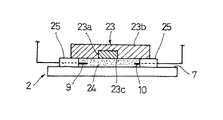
In FIG. 2, 23 is a metal material formed by joining magnetic stainless steel and an Ag (silver) alloy, 23a is magnetic stainless steel, 23b is an Ag alloy, and both are flush with each other at the joint 23c side. Are joined together. The
[0021]
As shown in FIG. 2, a gelling
[0022]
As described above, when the
[0023]
That is, the
[0024]
Furthermore, by moving the
[0025]
The image display is performed as follows, for example. Now, assuming that the image size is 1 cm × 2 cm and the pixel size is 100 μm, the pH values at the respective measurement points (100 × 200) are arranged corresponding to the position coordinates of the measurement points. The arranged values are displayed as a chemical image similar to an STM (scanning tunneling microscope) image, for example, corresponding to a gray scale or a color scale.
[0026]
FIG. 3 shows an example of a chemical image obtained by measuring a change in pH over time caused by corrosion at the joint 23b, which is an evaluation target portion of the
[0027]
As understood from the above description, the optical scanning type two-dimensional concentration distribution measuring apparatus used in the material evaluation method of the present invention can accurately and quickly grasp a minute pH change in a minute region, This can be processed and displayed as a two-dimensional image on the screen of the
[0028]
In the above-described embodiment, the
[0029]
And in this invention, it has comprised as shown in FIG. In FIG. 4 ,
[0030]
An
[0031]
In the embodiment shown in FIG. 4, the
[0032]
FIG. 5 shows another embodiment. In the optical scanning type two-dimensional concentration distribution measuring apparatus shown in FIG. 5, all portions of the measuring apparatus
[0033]
In the two-dimensional ion concentration measurement apparatus used in each of the above-described embodiments, the reference electrode RE may be omitted and a bias voltage may be applied via the counter electrode CE. However, the bias voltage can be applied to the semiconductor substrate 5 more stably when the comparison electrode RE is provided.
[0034]
In each of the optical scanning type two-dimensional concentration distribution measuring devices, instead of moving the
[0035]
Further, in the optical scanning type two-dimensional concentration distribution measuring apparatus, the
[0036]
Furthermore, in each of the above embodiments, the two-dimensional distribution state of hydrogen ions (pH) is captured, and the
[0037]
By the way, although the material evaluation method mentioned above observed the distribution change of pH in the
[0038]
FIG. 6 shows another embodiment of the present invention. The optical scanning type two-dimensional concentration distribution measuring apparatus shown in FIG. 6 is SnO 2 (tin oxide) on the upper surface of the
[0039]
For example, in order to evaluate the
[0040]
The change in the gas concentration is detected by the gas
[0041]
In the above embodiment, when the gas
[0042]
Also in the optical scanning type two-dimensional concentration distribution measuring apparatus of the above embodiment, instead of moving the
[0043]
Further, in the optical scanning type two-dimensional concentration distribution measuring apparatus, the
[0044]
And in the above-mentioned embodiment, the change in the two-dimensional distribution of the ion concentration and gas concentration was detected, but the material evaluation method of the present invention is not limited to these, the compound concentration, Furthermore, a change in the distribution of characteristic parameters such as a redox potential may be detected.
[0045]
In addition, the material evaluation method of the present invention is not limited to the above-mentioned metal materials, but also the biological fluid properties of artificial bone materials, the corrosion resistance of denture fittings, the covering degree of coating materials, the passage properties of artificial membranes, It can be applied to their evaluation over a wide range of metallic materials, organic materials, inorganic materials such as exchangers.
[0046]
【The invention's effect】
According to the material evaluation method of the present invention, various materials can be evaluated more easily and quickly than in the past. And since evaluation of various materials can be directly evaluated according to the substance, it can evaluate accurately and reliably. In addition, the number of samples used for evaluation is small, and the reproducibility is excellent.
[Brief description of the drawings]
FIG. 1 is a diagram schematically showing an overall configuration of an apparatus used for a material evaluation method.
FIG. 2 is an enlarged cross-sectional view showing a main part of the device.
FIG. 3 is a diagram showing an example of data obtained by the material evaluation method.
FIG. 4 is a cross sectional view schematically showing a main part of an apparatus used for a material evaluation method according to an embodiment of the present invention .
FIG. 5 is a diagram schematically showing an overall configuration of an apparatus used in a material evaluation method according to another embodiment.
FIG. 6 is a diagram schematically showing an overall configuration of an apparatus used in a material evaluation method according to another embodiment of the present invention .
[Explanation of symbols]
DESCRIPTION OF
Claims (1)
Priority Applications (3)
| Application Number | Priority Date | Filing Date | Title |
|---|---|---|---|
| JP13619297A JP3688096B2 (en) | 1997-05-10 | 1997-05-10 | Material evaluation method |
| US09/071,332 US6053035A (en) | 1997-05-10 | 1998-05-01 | Material evaluation method |
| EP98108468A EP0877243A1 (en) | 1997-05-10 | 1998-05-08 | Material evaluation method |
Applications Claiming Priority (1)
| Application Number | Priority Date | Filing Date | Title |
|---|---|---|---|
| JP13619297A JP3688096B2 (en) | 1997-05-10 | 1997-05-10 | Material evaluation method |
Publications (2)
| Publication Number | Publication Date |
|---|---|
| JPH10311818A JPH10311818A (en) | 1998-11-24 |
| JP3688096B2 true JP3688096B2 (en) | 2005-08-24 |
Family
ID=15169503
Family Applications (1)
| Application Number | Title | Priority Date | Filing Date |
|---|---|---|---|
| JP13619297A Expired - Fee Related JP3688096B2 (en) | 1997-05-10 | 1997-05-10 | Material evaluation method |
Country Status (3)
| Country | Link |
|---|---|
| US (1) | US6053035A (en) |
| EP (1) | EP0877243A1 (en) |
| JP (1) | JP3688096B2 (en) |
Families Citing this family (8)
| Publication number | Priority date | Publication date | Assignee | Title |
|---|---|---|---|---|
| JP2930181B2 (en) * | 1995-06-20 | 1999-08-03 | 松下電器産業株式会社 | Two-dimensional sensor for measuring nerve cell activity and measuring device using the same |
| JPH11101774A (en) * | 1997-09-26 | 1999-04-13 | Tsutomu Hoshimiya | Apparatus for inspecting and evaluating surface flaw of conductor |
| US7090757B2 (en) * | 2002-02-15 | 2006-08-15 | Ut-Battelle Llc | Photoelectrochemical molecular comb |
| DE10242529A1 (en) * | 2002-09-12 | 2004-03-25 | Forschungszentrum Jülich GmbH | Portable optical system using photosensitive electrode to analyze one or more substances, includes light sources inside analysis container |
| US7141150B1 (en) | 2004-07-19 | 2006-11-28 | The United States Of America As Represented By The Secretary Of The Navy | Method and test chamber for accelerated aging of materials and bonds subject to corrosion related degradation |
| US7209240B1 (en) | 2004-08-05 | 2007-04-24 | The United States Of America As Represented By The Secretary Of The Navy | System and apparatus for measuring displacements in electro-active materials |
| US7236252B1 (en) | 2004-08-05 | 2007-06-26 | The United States Of America As Repersented By The Secretary Of The Navy | System and apparatus for measuring displacements in electro-active materials |
| JP6097832B2 (en) * | 2013-07-22 | 2017-03-15 | 株式会社日立製作所 | Metal Corrosion Resistance Evaluation Method, Metal Material Corrosion Resistance Evaluation Device, Metal Material Composition Prediction Method, Metal Material Composition Prediction Device |
Family Cites Families (10)
| Publication number | Priority date | Publication date | Assignee | Title |
|---|---|---|---|---|
| US4591550A (en) * | 1984-03-01 | 1986-05-27 | Molecular Devices Corporation | Device having photoresponsive electrode for determining analytes including ligands and antibodies |
| US5500188A (en) * | 1984-03-01 | 1996-03-19 | Molecular Devices Corporation | Device for photoresponsive detection and discrimination |
| US4963815A (en) * | 1987-07-10 | 1990-10-16 | Molecular Devices Corporation | Photoresponsive electrode for determination of redox potential |
| US5200051A (en) * | 1988-11-14 | 1993-04-06 | I-Stat Corporation | Wholly microfabricated biosensors and process for the manufacture and use thereof |
| US5348627A (en) * | 1993-05-12 | 1994-09-20 | Georgia Tech Reserach Corporation | Process and system for the photoelectrochemical etching of silicon in an anhydrous environment |
| US5489515A (en) * | 1993-12-09 | 1996-02-06 | Avl Medical Instruments Ag | Device for analyzing the metabolism of cells |
| USH1563H (en) * | 1994-09-23 | 1996-07-02 | The United States Of America As Represented By The Secretary Of The Army | Chemical agent monitor for immunoassay detection |
| JPH08193937A (en) * | 1995-01-17 | 1996-07-30 | Hitachi Ltd | Electronic apparatus and corrosion monitor |
| US5567302A (en) * | 1995-06-07 | 1996-10-22 | Molecular Devices Corporation | Electrochemical system for rapid detection of biochemical agents that catalyze a redox potential change |
| JP2930181B2 (en) * | 1995-06-20 | 1999-08-03 | 松下電器産業株式会社 | Two-dimensional sensor for measuring nerve cell activity and measuring device using the same |
-
1997
- 1997-05-10 JP JP13619297A patent/JP3688096B2/en not_active Expired - Fee Related
-
1998
- 1998-05-01 US US09/071,332 patent/US6053035A/en not_active Expired - Fee Related
- 1998-05-08 EP EP98108468A patent/EP0877243A1/en not_active Withdrawn
Also Published As
| Publication number | Publication date |
|---|---|
| US6053035A (en) | 2000-04-25 |
| JPH10311818A (en) | 1998-11-24 |
| EP0877243A1 (en) | 1998-11-11 |
Similar Documents
| Publication | Publication Date | Title |
|---|---|---|
| Simões et al. | Use of SVET and SECM to study the galvanic corrosion of an iron–zinc cell | |
| Kounaves | Voltammetric techniques | |
| Bard et al. | Chemical imaging of surfaces with the scanning electrochemical microscope | |
| Wildgoose et al. | High‐temperature electrochemistry: a review | |
| Nakao et al. | High-resolution pH imaging sensor for microscopic observation of microorganisms | |
| Banks et al. | The transport limited currents at insonated electrodes | |
| US5489515A (en) | Device for analyzing the metabolism of cells | |
| JP3688096B2 (en) | Material evaluation method | |
| Ordeig et al. | Regular arrays of microdisc electrodes: simulation quantifies the fraction of ‘dead’electrodes | |
| Sagüés et al. | Kelvin Probe electrode for contactless potential measurement on concrete–Properties and corrosion profiling application | |
| Denuault et al. | Potentiometric probes | |
| Schmachtel et al. | New oxygen evolution anodes for metal electrowinning: investigation of local physicochemical processes on composite electrodes with conductive atomic force microscopy and scanning electrochemical microscopy | |
| Keddam et al. | Progress in scanning electrochemical microscopy by coupling with electrochemical impedance and quartz crystal microbalance | |
| JPH09292358A (en) | Zeta-potential measuring method using optical-scanning type two-dimensional concentration-distribution measuring device | |
| Pižeta et al. | Pseudopolarography of lead (II) in sediment and in interstitial water measured with a solid microelectrode | |
| JP3434124B2 (en) | Evaluation method of microcapsules | |
| JP3667566B2 (en) | Ion exchange membrane evaluation method | |
| Pähler et al. | Simultaneous visualization of surface topography and concentration field by means of scanning electrochemical microscopy using a single electrochemical probe and impedance spectroscopy | |
| JP3229812B2 (en) | Calibration method of optical scanning type two-dimensional pH distribution measuring device | |
| JP2000162080A (en) | Evaluation method for leak of liquid or gas in material | |
| JP2001183321A (en) | Method for evaluating photocatalytic film | |
| Rees et al. | Voltammetry as a probe of displacement | |
| JPH09166531A (en) | Two-dimensional distribution measuring method for microscopic substance | |
| JP2001337068A (en) | Cell and method for evaluating state of electrode reaction | |
| JP2835530B2 (en) | Scanning tunnel microscope |
Legal Events
| Date | Code | Title | Description |
|---|---|---|---|
| A621 | Written request for application examination |
Free format text: JAPANESE INTERMEDIATE CODE: A621 Effective date: 20040407 |
|
| A977 | Report on retrieval |
Free format text: JAPANESE INTERMEDIATE CODE: A971007 Effective date: 20041227 |
|
| A131 | Notification of reasons for refusal |
Free format text: JAPANESE INTERMEDIATE CODE: A131 Effective date: 20050308 |
|
| A521 | Written amendment |
Free format text: JAPANESE INTERMEDIATE CODE: A523 Effective date: 20050420 |
|
| TRDD | Decision of grant or rejection written | ||
| A01 | Written decision to grant a patent or to grant a registration (utility model) |
Free format text: JAPANESE INTERMEDIATE CODE: A01 Effective date: 20050531 |
|
| A61 | First payment of annual fees (during grant procedure) |
Free format text: JAPANESE INTERMEDIATE CODE: A61 Effective date: 20050607 |
|
| R150 | Certificate of patent or registration of utility model |
Free format text: JAPANESE INTERMEDIATE CODE: R150 |
|
| S531 | Written request for registration of change of domicile |
Free format text: JAPANESE INTERMEDIATE CODE: R313532 |
|
| R350 | Written notification of registration of transfer |
Free format text: JAPANESE INTERMEDIATE CODE: R350 |
|
| FPAY | Renewal fee payment (event date is renewal date of database) |
Free format text: PAYMENT UNTIL: 20110617 Year of fee payment: 6 |
|
| FPAY | Renewal fee payment (event date is renewal date of database) |
Free format text: PAYMENT UNTIL: 20130617 Year of fee payment: 8 |
|
| FPAY | Renewal fee payment (event date is renewal date of database) |
Free format text: PAYMENT UNTIL: 20130617 Year of fee payment: 8 |
|
| S533 | Written request for registration of change of name |
Free format text: JAPANESE INTERMEDIATE CODE: R313533 |
|
| FPAY | Renewal fee payment (event date is renewal date of database) |
Free format text: PAYMENT UNTIL: 20130617 Year of fee payment: 8 |
|
| R350 | Written notification of registration of transfer |
Free format text: JAPANESE INTERMEDIATE CODE: R350 |
|
| LAPS | Cancellation because of no payment of annual fees |