JP3682797B2 - Non-reciprocal circuit element - Google Patents
Non-reciprocal circuit element Download PDFInfo
- Publication number
- JP3682797B2 JP3682797B2 JP00288596A JP288596A JP3682797B2 JP 3682797 B2 JP3682797 B2 JP 3682797B2 JP 00288596 A JP00288596 A JP 00288596A JP 288596 A JP288596 A JP 288596A JP 3682797 B2 JP3682797 B2 JP 3682797B2
- Authority
- JP
- Japan
- Prior art keywords
- terminal
- metal case
- plate
- resin
- central conductor
- Prior art date
- Legal status (The legal status is an assumption and is not a legal conclusion. Google has not performed a legal analysis and makes no representation as to the accuracy of the status listed.)
- Expired - Lifetime
Links
Images


Description
【0001】
【発明の属する技術分野】
本発明は、アイソレータ・サーキュレータとして利用される非可逆回路素子に関するものである。
【0002】
【従来の技術】
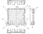
従来の非可逆回路素子の一例として、集中定数型アイソレータの一例の分解斜視図を図9に示す。この従来例は、下ケース65上にパターン電極の形成された誘電体基板63を配置し、フェライト64と互いに絶縁状態で重ね合わされた中心導体66とからなる中心導体部を誘電体基板に形成された穴に配置し、各中心導体と誘電体基板上の所定のパターン電極とを接続し、磁石67の装着された上ケース68を被せて構成されている。この誘電体基板63の69はダミー抵抗であり、70はアース電極である。このアース電極に接続されたダミー抵抗69により、中心導体の一つの端子が終端されている。
【0003】
【発明が解決しようとする課題】
従来の集中定数型アイソレータでは、例えば携帯電話等に使用されるため、小型化・薄型化の要求が強い。もちろん、使用に耐える電気特性を有することと低価格であることが同時に要求される。
この小型化を考えたとき、所望の電気特性を得るためには、フェライト64の外径がある程度必要であり、フェライト64の小型化には限界がある。そのため、全体を小型化してゆくと図10に示すように、フェライトが挿入される穴72が相対的に大きくなる。その結果、誘電体基板に強度的に弱い部分71ができ、生産工程での取り扱い時に基板が割れる危険性が高まり、量産性が低くなる。このため、従来の構造では、小型化が困難であった。
また、ダミー抵抗は、誘電体基板上に印刷された抵抗により形成されている。この誘電体基板では、放熱性が良くなく、しかも他の静電容量用及びアース用のパターン電極も形成されているので、スペース的にも余裕がない。このため、そのダミー抵抗部における耐電力が小さく、せいぜい1W程度の耐電力しか実現出来なかった。
従って、スペースを広げると小型化の流れに逆行し、比較的大きな耐電力を必要とする用途では、小型の集中定数型アイソレータを構成することが困難であった。
本発明は、上記のことを鑑みて、小型でしかも耐電力の大きい非可逆回路素子を提供する事を目的とする。
【0004】
【課題を解決するための手段】
第1の発明は、金属ケース下と、金属ケース上と、フェライトコアに中心導体を配置した中心導体部と、前記中心導体部と接続される板状コンデンサと、チップ抵抗と、永久磁石と、樹脂ケースを備えた非可逆回路素子であって、前記樹脂ケースは、対向する側面のそれぞれにアース端子と入出力端子を有し、前記樹脂ケースの内側には、前記アース端子とつながる導電体板で形成されたアース電極板と、前記アース電極板が配置されている面に形成された突起部と、前記突起部上に前記入出力端子とつながる他の導電体板で形成された回路接続端子を有し、前記導電体板のそれぞれは、その一部が樹脂部分に埋設してなり、該樹脂ケースの前記アース電極板上に前記突起部に対応した切り欠き部を備えた金属ケース下が設置され、該金属ケース下の内側底面に、フェライトコアを包むように折り畳まれた中心導体を有する中心導体部を配置し、フェライトコアの外周を係止する突起を有するとともに、外形が前記樹脂ケース及び前記金属ケース下の内側に収納される大きさの樹脂モールドを、前記中心導体部の上側に配置し、該樹脂モールドの上側に永久磁石を配置し、更に金属ケース上で覆う非可逆回路素子である。
第1の発明においては、前記チップ抵抗として、基板の一面に、抵抗膜とその抵抗膜の両端に端子電極が形成され、前記端子電極の一方には前記中心導体が接続され、前記基板の一面の裏面側には、前記端子電極の他方と導通した裏面側端子電極が形成されたチップ抵抗を用い、該チップ抵抗を前記裏面側端子電極でアース接続するのが好ましい。
第2の発明は、金属ケース下と、金属ケース上と、フェライトコアに中心導体を配置した中心導体部と、前記中心導体部と接続される板状コンデンサと、チップ抵抗と、永久磁石と、樹脂ケースを備えた非可逆回路素子であって、前記樹脂ケースは、対向する側面のそれぞれにアース端子と入出力端子を有し、前記樹脂ケースの内側には、前記アース端子とつながる導電体板で形成されたアース電極板と、前記アース電極板が配置されている面に形成された突起部と、前記突起部上に前記入出力端子とつながる他の導電体板で形成された回路接続端子を有し、前記導電体板のそれぞれは、その一部が樹脂部分に埋設してなり、前記板状コンデンサは、誘電体板の上下面に電極が形成されており、前記チップ抵抗は、基板の一面に、抵抗膜とその抵抗膜の両端に端子電極が形成され、前記端子電極の一方には前記中心導体が接続され、前記基板の一面の裏面側には、前記端子電極の他方と導通した裏面側端子電極が形成されており、前記中心導体部は、フェライトコアを包むように折り畳まれた3つの中心導体を有し、前記樹脂ケースのアース電極板上に前記金属ケース下が設置され、前記金属ケース下の上に前記中心導体部、前記板状コンデンサ、前記チップ抵抗を配置して、それぞれを前記金属ケース下と直接アース接続し、前記板状コンデンサのうちの一つと前記チップ抵抗とが、一つの中心導体の端部で互いに接続され、前記板状コンデンサのうちの他の二つは、その上面電極が、前記樹脂突起部に形成された回路接続端子と略同じ高さであって、他の二つの中心導体の端部で、それぞれ前記回路接続端子に接続される非可逆回路素子である。
第2の発明の非可逆回路素子においては、前記板状コンデンサは、前記電極の一方に中心導体の先端部が接続され、他方の電極が金属ケース下に接続され、前記チップ抵抗は、前記裏面側端子電極が金属ケース下に接続するのが好ましい。
【0005】
【発明の実施の態様】
本発明に係る一実施例の分解斜視図を図1に示す。この実施例について説明する。まず、最下部に樹脂ケース1がある。この樹脂ケース1の平面図とその3方向の側面図を図2に、底面図を図3に示す。この図2、3において、導体部分を斜線で示す。又、図2のA−A’断面図を図4に、B−B’断面図を図5に示す。この樹脂ケース1は、3つの導電体板が樹脂部分と一体に形成されている。この1つの導電体板は、アース電極板2であり、樹脂ケース1の底部に広く配置され、それとつながるアース端子3が樹脂ケース1の装着面となる裏面に導出されている。また、他の2つの導電体板は、入出力端子用であり、内側の回路接続端子4と外側の入出力端子5とがつながったコ字状の導電体板である。この内側回路接続端子4は、アース板電極2の配置されている面に突起部6が形成され、その突起部6の上に配置されている。
【0006】
この樹脂ケース1の上に、金属ケース下7が載せられる。この金属ケース下7は、樹脂ケース1の突起部6に対応する切り欠き部8を有し、この樹脂ケース1のアース電極板2と半田付けされる。
この金属ケース下7の上に、誘電体板の上下面に電極が形成された板状コンデンサ9とチップ抵抗10と、フェライトコア11上に中心導体12を互いに絶縁状態で、120度の間隔で回転対称に配置された中心導体部とを配置する。この中心導体部は、図6に示すように、円板部14から120度間隔で放射状に伸びるそれぞれ2本の導体からなり、先端で接続されている3つの中心導体12からなり、その円板部14上にフェライトコア11を配置し、各中心導体14を折り曲げ、各中心導体間に絶縁シートを挟んで構成されている。そして、3つの中心導体12のうち、2つの中心導体12の先端部13a、13bは、それぞれ板状コンデンサ9と樹脂ケース1上の内側回路接続端子4に接続され、他の一つの中心導体の先端部13cは、板状コンデンサ9とチップ抵抗10に接続される。この中心導体部の円板部14は金属ケース下7に接続され、アース接続される。又、板状コンデンサ9も中心導体の先端部が接続される面の対向面側で金属ケース下7に接続され、アース接続される。
【0007】
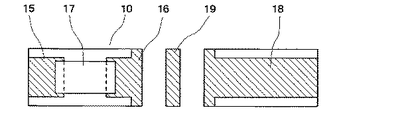
このチップ抵抗10の平面図、側面図、底面図を図7に示す。このチップ抵抗10は、一面に2つの端子電極15、16を有し、その端子電極間に酸化ルテニウムによる抵抗膜17が形成されている。この抵抗膜上には絶縁コートが施されている。また一方の端子電極16は、側面に形成された電極19を介して、底面の端子電極18と導通している。そして、一つの中心導体の先端部13cは、チップ抵抗10の端子電極15と接続され、そして、そのチップ抵抗10の端子電極18が金属ケース下7と接続され、アース接続される。
【0008】
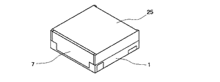
次に、この中心導体部に樹脂モールド20を被せる。この樹脂モールド20は、中央にフェライトコアの外径とほぼ同じ大きさの貫通孔21を有し、下部にフェライトコア11の外周部に当接するようなつめ部22が3ヶ所形成されている。このつめ部22は、フェライトコアの側面の中心導体の部分に位置し、フェライトコアの位置決めを行うとともに、フェライトコア側面の中心導体の保護・絶縁も兼ねている。この樹脂モールド20は、外形が樹脂ケース1及び金属ケース下7の内側に収納される大きさであり、上面に磁石24を位置決めする突出部23が形成されている。そして、この突出部23で位置決めされる位置に磁石24が配置される。そして、金属ケース上25を被せ、金属ケース上25と金属ケース下7とを半田付けして非可逆回路素子を構成した。
この金属ケース上25の側面の一つの対向面26は、金属ケース下7の側面28の内側に挿入され、半田付けされる。他の対向面27は、樹脂ケース1の側面29の上端上に位置する。
この実施例は、集中定数型アイソレータであり、その斜視図を図8に示す。
【0009】
上記実施例は、中心導体の12の一つをチップ抵抗10に接続し、終端しているので、アイソレータとなっているが、その中心導体を終端しないで入出力端子とすれば、サーキュレータとして使用出来る。
【0010】
本発明の実施例では、樹脂ケース1の内側回路接続端子4が形成されている突起部6の高さを、板状コンデンサ9とほぼ同一としておき、中心導体12の先端部13a、13bの接続を容易としている。また、この突起部6により、この接続端子4とアース電極板2の絶縁を確実にしている。また、この樹脂ケース1により、表面実装が可能となる。
また本発明のチップ抵抗10は、一方の端子電極16が側面を介して底面に導出され、底面に端子電極18が形成され、その端子電極18により、金属ケース下7の上にその底面を直接接続したので、広い面積で金属ケース下と接続され、放熱性が高く、接続も容易である。放熱性の改善により、耐電力を改善出来る。また本発明の実施例では、フェライトコアと磁石とを一つの樹脂モールドで位置決めするので、位置決めが容易であるとともに、取り付けも容易である。又、この樹脂モールドのつめ部がフェライトコア側面の中心導体をカバーしているので、このフェライトコア側面の中心導体と板状コンデンサとのショートを防止している。
この実施例の構造によれば、フェライトコアの大きさを相対的に大きくしても、従来のような誘電体基板を用いないので、小型化を達成出来る。
【0011】
【発明の効果】
本発明により、小型で耐電力も大きい集中定数型アイソレータを得ることができ、例えば携帯電話等においてミスマッチングによる耐反射電力の増加によるアンプの保護に、極めて有効なものである。
【図面の簡単な説明】
【図1】本発明に係る一実施例の分解斜視図である。
【図2】本発明に係る一実施例の樹脂ケースの平面図及び側面図である。
【図3】本発明に係る一実施例の樹脂ケースの底面図である。
【図4】図1のA−A’断面図である。
【図5】図1のB−B’断面図である。
【図6】本発明に係る一実施例の中心導体の平面図である。
【図7】本発明に係る一実施例のチップ抵抗の平面図、側面図及び底面図である。
【図8】本発明に係る一実施例の斜視図である。
【図9】従来例の分解斜視図である。
【図10】従来例の誘電体基板の平面図である。
【符号の説明】
1 樹脂ケース
2 アース電極板
3 アース端子
4 内側回路接続端子
5 入出力端子
6 突起部
7 金属ケース下
8 切り欠き部
9 板状コンデンサ
10 チップ抵抗
11 フェライトコア
12 中心導体
13a、13b、13c 先端部
14 円板部
15、16、18 端子電極
17 抵抗膜
19 電極
20 樹脂モールド
21 貫通孔
22 つめ部
23 突出部
24 磁石
25 金属ケース上
26、27 対向面
28、29 側面[0001]
BACKGROUND OF THE INVENTION
The present invention relates to a nonreciprocal circuit device used as an isolator / circulator.
[0002]
[Prior art]
FIG. 9 shows an exploded perspective view of an example of a lumped constant type isolator as an example of a conventional non-reciprocal circuit device. In this conventional example, a
[0003]
[Problems to be solved by the invention]
Since conventional lumped constant isolators are used for mobile phones, for example, there is a strong demand for miniaturization and thinning. Of course, it is required to have electrical characteristics that can withstand use and to be inexpensive.
Considering this miniaturization, the outer diameter of the
The dummy resistor is formed by a resistor printed on a dielectric substrate. In this dielectric substrate, heat dissipation is not good, and other electrostatic capacity and ground pattern electrodes are also formed, so there is no room in terms of space. For this reason, the power resistance in the dummy resistance portion is small, and only a power resistance of about 1 W can be realized.
Therefore, if the space is expanded, the size of the device is reversed against the trend of miniaturization, and it is difficult to construct a small lumped constant isolator for applications that require a relatively large power resistance.
In view of the above, it is an object of the present invention to provide a nonreciprocal circuit device that is small in size and has high power durability.
[0004]
[Means for Solving the Problems]
According to a first aspect of the present invention, a metal case, a metal case, a central conductor portion having a central conductor disposed in a ferrite core, a plate capacitor connected to the central conductor portion, a chip resistor, a permanent magnet , the irreversible circuit element including a resin case, the resin case has a respective output terminal and ground terminal of the opposing sides on the inside of the resin case, conductive plate connected to the ground terminal A circuit connection terminal formed by a ground electrode plate formed by the above, a projection formed on a surface on which the ground electrode plate is disposed, and another conductor plate connected to the input / output terminal on the projection Each of the conductor plates is partially embedded in a resin portion, and a metal case provided with a notch portion corresponding to the protrusion on the ground electrode plate of the resin case. Installed, the metal casing The inner bottom surface of the bottom scan, place the central conductor portion having a central conductor folded to wrap the ferrite core, as well as have a projection for locking the outer periphery of the ferrite core, under external shape of the resin case and the metal case the size of the resin mold that is the housed inside, is arranged on the upper side of the central conductor portion, a permanent magnet is disposed on the upper side of the resin mold, is a non-reciprocal circuit element to cover over the metal case.
In the first invention, as the chip resistor, a resistance film and a terminal electrode are formed on both ends of the resistance film on one surface of the substrate, the central conductor is connected to one of the terminal electrodes, and the one surface of the substrate It is preferable that a chip resistor having a back-side terminal electrode that is electrically connected to the other of the terminal electrodes is used on the back side of the chip, and the chip resistor is grounded by the back-side terminal electrode.
According to a second aspect of the present invention, a metal case, a metal case, a central conductor portion having a central conductor disposed in a ferrite core, a plate capacitor connected to the central conductor portion, a chip resistor, a permanent magnet , the irreversible circuit element including a resin case, the resin case has a respective output terminal and ground terminal of the opposing sides on the inside of the resin case, conductive plate connected to the ground terminal A circuit connection terminal formed by a ground electrode plate formed by the above, a projection formed on a surface on which the ground electrode plate is disposed, and another conductor plate connected to the input / output terminal on the projection Each of the conductor plates is partially embedded in a resin portion, the plate capacitor has electrodes formed on the upper and lower surfaces of the dielectric plate, and the chip resistor On one side Terminal electrodes are formed at both ends of the resistance film, the central conductor is connected to one of the terminal electrodes, and a back-side terminal electrode that is electrically connected to the other of the terminal electrodes is formed on the back side of the one surface of the substrate. The center conductor portion has three center conductors folded so as to wrap the ferrite core, the metal case bottom is installed on the ground electrode plate of the resin case, and the metal case bottom is above the metal case A central conductor portion, the plate capacitor, and the chip resistor are arranged, and each of them is directly grounded to the bottom of the metal case, and one of the plate capacitors and the chip resistor are connected to an end of one central conductor. The other two of the plate capacitors are connected to each other at the same portion, and the other two central conductors have upper surface electrodes that are substantially the same height as the circuit connection terminals formed on the resin protrusions. End of A non-reciprocal circuit element connected to each of the circuit connecting terminals.
In the nonreciprocal circuit device according to a second aspect of the present invention, the plate capacitor has one end of the center conductor connected to one of the electrodes, the other electrode connected under the metal case, and the chip resistor connected to the back surface. The side terminal electrode is preferably connected under the metal case.
[0005]
BEST MODE FOR CARRYING OUT THE INVENTION
An exploded perspective view of an embodiment according to the present invention is shown in FIG. This embodiment will be described. First, there is a
[0006]
A metal case lower 7 is placed on the
On the
[0007]
A plan view, a side view, and a bottom view of the
[0008]
Next, the
One opposing
This embodiment is a lumped constant type isolator, and a perspective view thereof is shown in FIG.
[0009]
In the above embodiment, one of the
[0010]
In the embodiment of the present invention, the height of the
In the
According to the structure of this embodiment, even if the size of the ferrite core is relatively increased, the conventional dielectric substrate is not used, so that a reduction in size can be achieved.
[0011]
【The invention's effect】
According to the present invention, it is possible to obtain a lumped constant isolator that is small in size and has high power resistance, and is extremely effective for protecting an amplifier due to an increase in reflection power resistance due to mismatching in, for example, a mobile phone.
[Brief description of the drawings]
FIG. 1 is an exploded perspective view of an embodiment according to the present invention.
FIG. 2 is a plan view and a side view of a resin case according to an embodiment of the present invention.
FIG. 3 is a bottom view of a resin case according to an embodiment of the present invention.
4 is a cross-sectional view taken along line AA ′ of FIG.
FIG. 5 is a cross-sectional view taken along the line BB ′ of FIG.
FIG. 6 is a plan view of a central conductor according to an embodiment of the present invention.
7 is a plan view, a side view, and a bottom view of a chip resistor according to an embodiment of the present invention. FIG.
FIG. 8 is a perspective view of an embodiment according to the present invention.
FIG. 9 is an exploded perspective view of a conventional example.
FIG. 10 is a plan view of a conventional dielectric substrate.
[Explanation of symbols]
DESCRIPTION OF
Claims (4)
前記樹脂ケースは、対向する側面のそれぞれにアース端子と入出力端子を有し、
前記樹脂ケースの内側には、前記アース端子とつながる導電体板で形成されたアース電極板と、前記アース電極板が配置されている面に形成された突起部と、前記突起部上に前記入出力端子とつながる他の導電体板で形成された回路接続端子を有し、前記導電体板のそれぞれは、その一部が樹脂部分に埋設してなり、
該樹脂ケースの前記アース電極板上に前記突起部に対応した切り欠き部を備えた金属ケース下が設置され、該金属ケース下の内側底面に、フェライトコアを包むように折り畳まれた中心導体を有する中心導体部を配置し、
フェライトコアの外周を係止する突起を有するとともに、外形が前記樹脂ケース及び前記金属ケース下の内側に収納される大きさの樹脂モールドを、前記中心導体部の上側に配置し、
該樹脂モールドの上側に永久磁石を配置し、更に金属ケース上で覆うことを特徴とする非可逆回路素子。A non-metal case comprising a metal case, a metal case, a central conductor portion having a central conductor disposed on a ferrite core, a plate capacitor connected to the central conductor portion, a chip resistor, a permanent magnet, and a resin case. A reversible circuit element,
The resin case has a ground terminal and an input / output terminal on each of opposite side surfaces,
The inside of the resin case, and the earth electrode plate formed of conductive plate connected to the ground terminal, and a protruding portion to which the ground electrode plate is formed on a surface that is located, entering-on the protrusion It has a circuit connection terminal formed of another conductor plate connected to the output terminal, each of the conductor plates is embedded in a resin part,
The bottom of the metal case having a notch corresponding to the protruding portion is installed on the ground electrode plate of the resin case, and the inner bottom surface under the metal case has a center conductor folded so as to wrap the ferrite core. Place the central conductor,
As well as have a projection for locking the outer periphery of the ferrite core, the size of the resin mold contour is housed inside under the resin case and the metal case, it is arranged on the upper side of the center conductor portion,
Nonreciprocal circuit device in which the permanent magnets on the upper side of the resin mold is placed, further characterized in that the covering on the metal case.
前記樹脂ケースは、対向する側面のそれぞれにアース端子と入出力端子を有し、
前記樹脂ケースの内側には、前記アース端子とつながる導電体板で形成されたアース電極板と、前記アース電極板が配置されている面に形成された突起部と、前記突起部上に前記入出力端子とつながる他の導電体板で形成された回路接続端子を有し、前記導電体板のそれぞれは、その一部が樹脂部分に埋設してなり、
前記板状コンデンサは、誘電体板の上下面に電極が形成されており、
前記チップ抵抗は、基板の一面に、抵抗膜とその抵抗膜の両端に端子電極が形成され、前記端子電極の一方には前記中心導体が接続され、前記基板の一面の裏面側には、前記端子電極の他方と導通した裏面側端子電極が形成されており、
前記中心導体部は、フェライトコアを包むように折り畳まれた3つの中心導体を有し、
前記樹脂ケースのアース電極板上に前記金属ケース下が設置され、前記金属ケース下の上に前記中心導体部、前記板状コンデンサ、前記チップ抵抗を配置して、それぞれを前記金属ケース下と直接アース接続し、
前記板状コンデンサのうちの一つと前記チップ抵抗とが、一つの中心導体の端部で互いに接続され、
前記板状コンデンサのうちの他の二つは、その上面電極が、前記樹脂突起部に形成された回路接続端子と略同じ高さであって、他の二つの中心導体の端部で、それぞれ前記回路接続端子に接続されることを特徴とする非可逆回路素子。A non-metal case comprising a metal case, a metal case, a central conductor portion having a central conductor disposed on a ferrite core, a plate capacitor connected to the central conductor portion, a chip resistor, a permanent magnet, and a resin case. A reversible circuit element,
The resin case has a ground terminal and an input / output terminal on each of opposite side surfaces,
The inside of the resin case, and the earth electrode plate formed of conductive plate connected to the ground terminal, and a protruding portion to which the ground electrode plate is formed on a surface that is located, entering-on the protrusion It has a circuit connection terminal formed of another conductor plate connected to the output terminal, each of the conductor plates is embedded in a resin part,
The plate capacitor has electrodes formed on the upper and lower surfaces of a dielectric plate,
The chip resistor has a resistance film and a terminal electrode formed on both ends of the resistance film on one surface of the substrate, the central conductor is connected to one of the terminal electrodes, A back side terminal electrode that is electrically connected to the other of the terminal electrodes is formed,
The central conductor portion has three central conductors folded so as to wrap the ferrite core,
The bottom of the metal case is installed on the ground electrode plate of the resin case, and the central conductor portion, the plate capacitor, and the chip resistor are arranged on the bottom of the metal case, and each is directly below the metal case. Connect to ground,
One of the plate capacitors and the chip resistor are connected to each other at the end of one central conductor,
The other two of the plate capacitors have upper surface electrodes that are substantially the same height as the circuit connection terminals formed on the resin protrusions, respectively, at the ends of the other two central conductors. A nonreciprocal circuit element connected to the circuit connection terminal.
Priority Applications (1)
| Application Number | Priority Date | Filing Date | Title |
|---|---|---|---|
| JP00288596A JP3682797B2 (en) | 1996-01-11 | 1996-01-11 | Non-reciprocal circuit element |
Applications Claiming Priority (1)
| Application Number | Priority Date | Filing Date | Title |
|---|---|---|---|
| JP00288596A JP3682797B2 (en) | 1996-01-11 | 1996-01-11 | Non-reciprocal circuit element |
Related Child Applications (1)
| Application Number | Title | Priority Date | Filing Date |
|---|---|---|---|
| JP2003117108A Division JP3788790B2 (en) | 2003-04-22 | 2003-04-22 | Non-reciprocal circuit element |
Publications (2)
| Publication Number | Publication Date |
|---|---|
| JPH09199909A JPH09199909A (en) | 1997-07-31 |
| JP3682797B2 true JP3682797B2 (en) | 2005-08-10 |
Family
ID=11541821
Family Applications (1)
| Application Number | Title | Priority Date | Filing Date |
|---|---|---|---|
| JP00288596A Expired - Lifetime JP3682797B2 (en) | 1996-01-11 | 1996-01-11 | Non-reciprocal circuit element |
Country Status (1)
| Country | Link |
|---|---|
| JP (1) | JP3682797B2 (en) |
Families Citing this family (4)
| Publication number | Priority date | Publication date | Assignee | Title |
|---|---|---|---|---|
| DE19734097A1 (en) * | 1997-08-07 | 1999-02-11 | Philips Patentverwaltung | Microwave device |
| KR100320934B1 (en) * | 1997-12-09 | 2002-05-13 | 이형도 | Internal terminal of isolator |
| CN111403884A (en) * | 2020-03-27 | 2020-07-10 | 深圳市信维通信股份有限公司 | Manufacturing method of patch type circulator |
| CN116525299B (en) * | 2023-07-04 | 2023-11-07 | 西南应用磁学研究所(中国电子科技集团公司第九研究所) | Plastic package shell applying multilayer chip capacitor and isolator composed of plastic package shell |
-
1996
- 1996-01-11 JP JP00288596A patent/JP3682797B2/en not_active Expired - Lifetime
Also Published As
| Publication number | Publication date |
|---|---|
| JPH09199909A (en) | 1997-07-31 |
Similar Documents
| Publication | Publication Date | Title |
|---|---|---|
| JPH0628195B2 (en) | Electric filter connector | |
| US5017894A (en) | Lumped constant non-reciprocal circuit element | |
| JP3682797B2 (en) | Non-reciprocal circuit element | |
| JP2721306B2 (en) | Lumped constant type non-reciprocal circuit device | |
| JP3788790B2 (en) | Non-reciprocal circuit element | |
| JPH04345201A (en) | Irreversible circuit component and center conductor for irreversible circuit component | |
| JP3209418B2 (en) | Dummy resistor for lumped constant type isolator | |
| JP4151789B2 (en) | Non-reciprocal circuit element | |
| US20010035798A1 (en) | Nonreciprocal circuit device and communication device | |
| JP3702595B2 (en) | Non-reciprocal circuit element | |
| JPH11205011A (en) | Irreversible circuit element of concentrated constant type | |
| US6796840B2 (en) | Surface mounting type non-reversible circuit element having superior productivity | |
| JP3944833B2 (en) | Non-reciprocal circuit element | |
| JP2000174508A (en) | Concentrated constant type irreversible circuit element | |
| US6930566B2 (en) | Small nonreciprocal circuit element that can be easily wired | |
| JP3762697B2 (en) | Non-reciprocal circuit element | |
| JPS6016086Y2 (en) | Wideband lumped constant circulator | |
| JP3655591B2 (en) | Non-reciprocal circuit element | |
| JP3092228U (en) | Non-reciprocal circuit device | |
| JP3579328B2 (en) | Non-reciprocal circuit device for VHF band and private wireless communication device | |
| JPS6016085Y2 (en) | Broadband lumped constant type circulator | |
| JP3093563U (en) | Isolator | |
| JPH0626281B2 (en) | Lumped isolator | |
| JPH11168304A (en) | Concentrated constant irreversible circuit element | |
| US7138883B2 (en) | Non-reciprocal circuit element |
Legal Events
| Date | Code | Title | Description |
|---|---|---|---|
| A521 | Written amendment |
Free format text: JAPANESE INTERMEDIATE CODE: A523 Effective date: 20040709 |
|
| A977 | Report on retrieval |
Free format text: JAPANESE INTERMEDIATE CODE: A971007 Effective date: 20041025 |
|
| A131 | Notification of reasons for refusal |
Free format text: JAPANESE INTERMEDIATE CODE: A131 Effective date: 20041029 |
|
| A521 | Written amendment |
Free format text: JAPANESE INTERMEDIATE CODE: A523 Effective date: 20041227 |
|
| A131 | Notification of reasons for refusal |
Free format text: JAPANESE INTERMEDIATE CODE: A131 Effective date: 20050304 |
|
| A521 | Written amendment |
Free format text: JAPANESE INTERMEDIATE CODE: A523 Effective date: 20050412 |
|
| TRDD | Decision of grant or rejection written | ||
| A01 | Written decision to grant a patent or to grant a registration (utility model) |
Free format text: JAPANESE INTERMEDIATE CODE: A01 Effective date: 20050506 |
|
| A61 | First payment of annual fees (during grant procedure) |
Free format text: JAPANESE INTERMEDIATE CODE: A61 Effective date: 20050519 |
|
| R150 | Certificate of patent or registration of utility model |
Free format text: JAPANESE INTERMEDIATE CODE: R150 |
|
| FPAY | Renewal fee payment (event date is renewal date of database) |
Free format text: PAYMENT UNTIL: 20090603 Year of fee payment: 4 |
|
| FPAY | Renewal fee payment (event date is renewal date of database) |
Free format text: PAYMENT UNTIL: 20100603 Year of fee payment: 5 |
|
| FPAY | Renewal fee payment (event date is renewal date of database) |
Free format text: PAYMENT UNTIL: 20100603 Year of fee payment: 5 |
|
| FPAY | Renewal fee payment (event date is renewal date of database) |
Free format text: PAYMENT UNTIL: 20110603 Year of fee payment: 6 |
|
| FPAY | Renewal fee payment (event date is renewal date of database) |
Free format text: PAYMENT UNTIL: 20110603 Year of fee payment: 6 |
|
| FPAY | Renewal fee payment (event date is renewal date of database) |
Free format text: PAYMENT UNTIL: 20120603 Year of fee payment: 7 |
|
| FPAY | Renewal fee payment (event date is renewal date of database) |
Free format text: PAYMENT UNTIL: 20120603 Year of fee payment: 7 |
|
| FPAY | Renewal fee payment (event date is renewal date of database) |
Free format text: PAYMENT UNTIL: 20130603 Year of fee payment: 8 |
|
| EXPY | Cancellation because of completion of term |