JP3673479B2 - Voltage regulator - Google Patents
Voltage regulator Download PDFInfo
- Publication number
- JP3673479B2 JP3673479B2 JP2001060175A JP2001060175A JP3673479B2 JP 3673479 B2 JP3673479 B2 JP 3673479B2 JP 2001060175 A JP2001060175 A JP 2001060175A JP 2001060175 A JP2001060175 A JP 2001060175A JP 3673479 B2 JP3673479 B2 JP 3673479B2
- Authority
- JP
- Japan
- Prior art keywords
- voltage
- current
- mirror circuit
- mos transistor
- current mirror
- Prior art date
- Legal status (The legal status is an assumption and is not a legal conclusion. Google has not performed a legal analysis and makes no representation as to the accuracy of the status listed.)
- Expired - Lifetime
Links
Images

Landscapes
- Continuous-Control Power Sources That Use Transistors (AREA)
- Amplifiers (AREA)
- Control Of Electrical Variables (AREA)
Description
【0001】
【発明の属する技術分野】
本発明は、ボルテージレギュレータに関し、特に低電圧動作及び低消費電流が要求される携帯機器等に使用されるボルテージレギュレータに関する。
【0002】
【従来の技術】
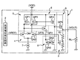
図3は、従来のボルテージレギュレータの回路例を示した図である。図3のボルテージレギュレータ100では、基準電圧発生回路101からの基準電圧VREFと、出力電圧VOUTの検出を行う検出回路104の抵抗102及び103で出力電圧VOUTが分圧された分圧電圧VFBは、差動増幅段105で電圧比較され、該比較結果に応じて出力段106をなすPチャネル型MOSトランジスタ(以下、PMOSトランジスタと呼ぶ)107の制御を行って一定の出力電圧VOUTが出力される。差動増幅段105は、カレントミラー回路を形成するPチャネル型MOSトランジスタ111,112と、差動対をなすNチャネル型MOSトランジスタ(以下、NMOSトランジスタと呼ぶ)113,114と、定電流源115とで構成されている。
【0003】
一方、図4は、従来のボルテージレギュレータの他の回路例を示した図であり、図4のボルテージレギュレータ100aは、図3の差動増幅段105と出力段106との間に、PMOSトランジスタ116及び定電流源117で構成された増幅段120を追加した3段の増幅段を備えるレギュレータであり、出力電圧VOUTの高速な制御を行うことができる。
【0004】
【発明が解決しようとする課題】
しかし、図3のボルテージレギュレータ100では、出力電圧VOUTが印加される負荷RLの抵抗値が小さい場合、PMOSトランジスタ107のゲート電圧が、差動増幅段105によって、ゲート−ソース間電圧Vgsを確保するために低い値に制御される。
【0005】
この場合、NMOSトランジスタ113における、しきい値をVthとすると共にドレイン−ソース間電圧をVdsとすると、定電流源115の両端に必要な電圧とNMOSトランジスタ113における(VREF−Vth+Vds)を加えた電圧よりも、PMOSトランジスタ107のゲート電圧を低くすることができなかった。このため、電源電圧VDDが低下したとき等、PMOSトランジスタ107に十分なゲート−ソース間電圧Vgsが確保することができなくなると、出力電圧VOUTは低下していく。すなわち、低電源電圧での正常な動作ができないという問題があった。
【0006】
これに対して、図4のボルテージレギュレータの場合、出力段106におけるPMOSトランジスタ107のゲート電圧は、ほぼ電源電圧VDDから接地電圧GNDまで制御できる。しかし、差動増幅段105、増幅段120及び出力段106の3段の増幅段を備えているため、特に低消費電流で動作させる場合、位相設計が難しくなることから、定電流源115及び117の各電流を合わせると、数十μA以上の電流が必要になり、低消費電流のボルテージレギュレータが必要な場合には消費電流が大きいという問題があった。
【0007】
本発明は、上記のような問題を解決するためになされたものであり、低消費電流で、かつ低電源電圧動作が可能であるボルテージレギュレータを得ることを目的とする。
【0008】
【課題を解決するための手段】
この発明に係るボルテージレギュレータは、あらかじめ設定された基準電圧を基に所定の電圧を生成して出力端子から出力するボルテージレギュレータにおいて、出力端子からの出力電圧の検出を行い、該検出した出力電圧に応じた電圧を生成して出力する検出回路部と、該検出回路部の出力電圧と上記基準電圧との差動増幅を行う1対のMOSトランジスタからなる差動対と、該差動対に対して所定のバイアス電流の供給を行う定電流源と、一方の出力端に接続された差動対における基準電圧が入力されるMOSトランジスタに対して負荷をなすと共に該MOSトランジスタに流れる電流に応じた電流を他方の出力端から出力する第1カレントミラー回路部と、一方の出力端に接続された差動対における検出回路部からの出力電圧が入力されるMOSトランジスタに対して負荷をなすと共に該MOSトランジスタに流れる電流に応じた電流を他方の出力端から出力する第2カレントミラー回路部と、第1カレントミラー回路部及び第2カレントミラー回路部の各他方の出力端に接続された第3カレントミラー回路部と、第2カレントミラー回路部と該第3カレントミラー回路部との接続部の電圧を接地電圧から電源電圧近傍まで制御可能であり、該接続部の電圧に応じた電流を上記出力端子から出力するMOSトランジスタを有する出力回路部とを備え、上記第1カレントミラー回路部は、差動対の負荷をなす第1MOSトランジスタと、該第1MOSトランジスタに流れる電流に応じた電流を他方の出力端から出力する第2MOSトランジスタとで構成され、上記第2カレントミラー回路部は、差動対の負荷をなす第3MOSトランジスタと、該第3MOSトランジスタに流れる電流に応じた電流を他方の出力端から出力する第4MOSトランジスタとで構成され、更に、第3カレントミラー回路部は、第1カレントミラー回路部の上記他方の出力端に接続された第5MOSトランジスタと、第2カレントミラー回路部の上記他方の出力端に接続された第6MOSトランジスタとで構成され、上記第1MOSトランジスタに対する上記第2MOSトランジスタのサイズの割合と、上記第3MOSトランジスタに対する上記第4MOSトランジスタのサイズの割合との比が、上記第5MOSトランジスタと上記第6MOSトランジスタのサイズ比に等しいものである。
【0009】
具体的には、上記第3カレントミラー回路部は、第1カレントミラー回路部の他方の出力端から流れる電流に応じた電流を第2カレントミラー回路部の他方の出力端に流すように動作する。
【0011】
【発明の実施の形態】
次に、図面に示す実施の形態に基づいて、本発明を詳細に説明する。
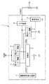
図1は、本発明の実施の形態におけるボルテージレギュレータの構成例を示したブロック図である。
図1において、ボルテージレギュレータ1は、所定の基準電圧VREFを生成して出力する基準電圧発生回路2と、出力電圧VOUTの検出を行い該検出した出力電圧VOUTに応じた電圧VFBを生成して出力する検出回路3と、基準電圧VREFと該検出回路3からの出力電圧VFBとの差動増幅を行う1対のトランジスタで構成された差動対4とを備えている。
【0012】
また、ボルテージレギュレータ1は、電源電圧VDDと差動対4の一方のトランジスタとの間に一方の出力端が接続された第1カレントミラー回路5と、電源電圧VDDと差動対4の他方のトランジスタとの間に一方の出力端が接続された第2カレントミラー回路6と、差動対4と接地との間に接続された定電流源7とを備えている。更に、ボルテージレギュレータ1は、第1カレントミラー回路5の他方の出力端及び第2カレントミラー回路6の他方の出力端が接続された第3カレントミラー回路8と、第2カレントミラー回路6と第3カレントミラー回路8との接続部の電圧に応じた電流を負荷RLに出力する出力回路9とを備えている。
【0013】
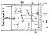
図2は、図1で示したボルテージレギュレータ1をCMOSで形成した場合を例にして示した回路図である。
図2において、検出回路3は、出力電圧VOUTと接地との間に接続された抵抗R1とR2との直列回路で構成されており、差動対4は、一対のNチャネル型MOSトランジスタ(以下、NMOSトランジスタと呼ぶ)QN1及びQN2で構成されている。検出回路3は、出力電圧VOUTを抵抗R1とR2で分圧して分圧電圧VFBを生成し出力する。NMOSトランジスタQN1のゲートには基準電圧VREFが、NMOSトランジスタQN2のゲートには分圧電圧VFBがそれぞれ入力されている。NMOSトランジスタQN1及びQN2の各ソースは接続され、該接続部は定電流源7を介して接地されている。
【0014】
また、第1カレントミラー回路5は、Pチャネル型MOSトランジスタ(以下、PMOSトランジスタと呼ぶ)QP1及びQP2で形成されている。PMOSトランジスタQP1のゲート及びドレイン並びにPMOSトランジスタQP2のゲートは接続され、PMOSトランジスタQP1及びQP2の各ソースはそれぞれ電源電圧VDDに接続されている。更に、PMOSトランジスタQP1のドレインは、差動対4をなすNMOSトランジスタQN1のドレインに接続され、PMOSトランジスタQP2のドレインは、第3カレントミラー回路8に接続されている。
【0015】
同様に、第2カレントミラー回路6は、PMOSトランジスタQP3及びQP4で形成されている。PMOSトランジスタQP3のゲート及びドレイン並びにPMOSトランジスタQP4のゲートは接続され、PMOSトランジスタQP3及びQP4の各ソースはそれぞれ電源電圧VDDに接続されている。更に、PMOSトランジスタQP3のドレインは、差動対4をなすNMOSトランジスタQN2のドレインに接続され、PMOSトランジスタQP4のドレインは、第3カレントミラー回路8に接続されている。
【0016】
第3カレントミラー回路8は、カレントミラー回路を形成する同一特性のNMOSトランジスタQN3及びQN4で構成されている。NMOSトランジスタQN3のゲート及びドレイン並びにNMOSトランジスタQN4のゲートは接続され、NMOSトランジスタQN3及びQN4の各ソースはそれぞれ接地されている。更に、NMOSトランジスタQN3のドレインは、第1カレントミラー回路5を形成するPMOSトランジスタQP2のドレインに接続され、NMOSトランジスタQN4のドレインは、第2カレントミラー回路6を形成するPMOSトランジスタQP4のドレインに接続されている。
【0017】
NMOSトランジスタQN4とPMOSトランジスタQP4との接続部は、出力回路9をなすPMOSトランジスタQP5のゲートに接続されている。出力回路9のPMOSトランジスタQP5において、ソースは電源電圧VDDに接続され、ドレインは検出回路3の抵抗R1に接続され、該接続部から出力電圧VOUTが出力される。該出力電圧VOUTは、負荷抵抗RLに印加される。
【0018】
ここで、差動対4において、基準電圧VREFと分圧電圧VFBが釣り合っている状態から、何らかの原因で出力電圧VOUTが低下した場合の各部の動作について説明する。出力電圧VOUTが低下すると分圧電圧VFBは低下し、NMOSトランジスタQN2のドレイン電流は、NMOSトランジスタQN1のドレイン電流よりも低下する。このため、PMOSトランジスタQP2のゲート電圧は低下すると共に、PMOSトランジスタQP4のゲート電圧は上昇し、NMOSトランジスタQN4において、ゲート−ソース電圧Vgsは上昇するがドレイン電流は低下することからドレイン−ソース電圧Vdsは低下する。従って、出力回路9のPMOSトランジスタQP5のゲート電圧は低下してPMOSトランジスタQP5の電流駆動能力が大きくなることにより、出力電圧VOUTを上昇させることができる。
【0019】
次に、差動対4において、基準電圧VREFと分圧電圧VFBが釣り合っている状態から、何らかの原因で出力電圧VOUTが上昇した場合の各部の動作について説明する。出力電圧VOUTが上昇すると分圧電圧VFBは上昇し、NMOSトランジスタQN2のドレイン電流は、NMOSトランジスタQN1のドレイン電流よりも増加する。このため、PMOSトランジスタQP2のゲート電圧は上昇すると共に、PMOSトランジスタQP4のゲート電圧は低下し、NMOSトランジスタQN4において、ゲート−ソース電圧Vgsは低下するがドレイン電流は増加することからドレイン−ソース電圧Vdsは上昇する。従って、出力回路9のPMOSトランジスタQP5のゲート電圧は上昇してPMOSトランジスタQP5の電流駆動能力が小さくなることにより、出力電圧VOUTを低下させることができる。
【0020】
一方、差動対4において、基準電圧VREFと分圧電圧VFBが釣り合っている状態の各部の動作について説明する。基準電圧VREFと分圧電圧VFBが釣り合っている場合、NMOSトランジスタQN1,QN2の各ドレイン電流及びPMOSトランジスタQP1,QP3の各ドレイン電流はそれぞれ等しくなる。従って、PMOSトランジスタQP1とカレントミラー回路を形成するPMOSトランジスタQP2のドレイン電流は、PMOSトランジスタQP1とQP2とのサイズ比に応じた値となる。同様に、PMOSトランジスタQP3とカレントミラー回路を形成するPMOSトランジスタQP4のドレイン電流は、PMOSトランジスタQP3とQP4とのサイズ比に応じた値となる。
【0021】
PMOSトランジスタQP1〜QP4は、同じサイズのトランジスタを使用するが、例えば消費電流を低下させたい場合は、PMOSトランジスタQP1とQP2のサイズ比及びPMOSトランジスタQP3とQP4とのサイズ比を共に小さくして調整する。また、例えば出力電圧VOUTの変動に対する動作速度を速くしたい場合は、PMOSトランジスタQP1とQP2のサイズ比及びPMOSトランジスタQP3とQP4とのサイズ比を共に大きくして調整する。なお、サイズ比とは、MOSトランジスタのゲート幅の比又はゲート長の比を示している。
【0022】
また、PMOSトランジスタQP1のサイズP1に対するPMOSトランジスタQP2のサイズP2の割合と、PMOSトランジスタQP3のサイズP3に対するPMOSトランジスタQP4のサイズP4の割合との比は、NMOSトランジスタQN3のサイズN3とNMOSトランジスタQN4のサイズN4との比に等しくなるように各MOSトランジスタを形成するとよい。すなわち、下記(1)式が成り立つように各MOSトランジスタを形成するとよい。
(P2/P1):(P4/P3)=N3:N4………………(1)
【0023】
このような構成にすることによって、出力回路9のPMOSトランジスタQP5のゲート電圧をほぼ電源電圧VDDから接地電圧まで制御することができ、より低い電源電圧VDDまでレギュレーション動作を行うことができる。例えば、定電流源7の両端に0.2V、差動対4をなすNMOSトランジスタQN1,QN2の各しきい値を0.3V、基準電圧VREFを0.6Vとすると、図3で示した従来のボルテージレギュレータよりも0.5V以上の低電圧化を行うことができる。また、PMOSトランジスタQP1とQP2、及びPMOSトランジスタQP3とQP4は、それぞれカレントミラー回路を構成し増幅段ではないことから、図3で示した従来のボルテージレギュレータと同様、2段の増幅段を備えたレギュレータであるため、消費電流を例えば数十μAから数uAに抑えて、位相設計をすることが可能となる。
【0024】
【発明の効果】
上記の説明から明らかなように、本発明のボルテージレギュレータによれば、出力端子からの出力電圧に応じた電圧を生成して出力する検出回路部と、該検出回路部の出力電圧と所定の基準電圧との差動増幅を行う差動対と、該差動対に対して所定のバイアス電流の供給を行う定電流源と、一方の出力端に接続された差動対の基準電圧が入力されるMOSトランジスタの負荷をなすと共に該MOSトランジスタに流れる電流に応じた電流を他方の出力端から出力する第1カレントミラー回路部と、一方の出力端に接続された差動対の検出回路部の出力電圧が入力されるMOSトランジスタの負荷をなすと共に該MOSトランジスタに流れる電流に応じた電流を他方の出力端から出力する第2カレントミラー回路部と、第1カレントミラー回路部及び第2カレントミラー回路部の各他方の出力端に接続された第3カレントミラー回路部と、第2カレントミラー回路部と該第3カレントミラー回路部との接続部の電圧を接地電圧から電源電圧近傍まで制御可能であり、該接続部の電圧に応じた電流を上記出力端子から出力するMOSトランジスタを有する出力回路部とを備えるようにした。このことから、低消費電流動作時における位相設計を容易にすることができるため消費電流の低減を図ることができると共に、低電源電圧での正常な動作を行うことができる。 また、第1MOSトランジスタに対する第2MOSトランジスタのサイズの割合と、第3MOSトランジスタに対する第4MOSトランジスタのサイズの割合との比は、第5MOSトランジスタと第6MOSトランジスタとのサイズ比に等しくなるようにした。このことから、低電源電圧時においても、出力電圧を所定の電圧で一定にすることができる。
【0025】
具体的には、第3カレントミラー回路部が、第1カレントミラー回路部の他方の出力端から流れる電流に応じた電流を第2カレントミラー回路部の他方の出力端に流すようにした。このことから、2段の増幅段を備えた構成にすることができ、消費電流を抑えて位相設計を容易に行うことができる。
【図面の簡単な説明】
【図1】 本発明の実施の形態におけるボルテージレギュレータの構成例を示したブロック図である。
【図2】 図1のボルテージレギュレータをCMOSで形成した場合を例にして示した回路図である。
【図3】 従来のボルテージレギュレータの回路例を示した図である。
【図4】 従来のボルテージレギュレータの他の回路例を示した図である。
【符号の説明】
1 ボルテージレギュレータ
2 基準電圧発生回路
3 検出回路
4 差動対
5 第1カレントミラー回路
6 第2カレントミラー回路
7 定電流源
8 第3カレントミラー回路
9 出力回路
RL 負荷[0001]
BACKGROUND OF THE INVENTION
The present invention relates to a voltage regulator, and more particularly to a voltage regulator used in a portable device that requires low voltage operation and low current consumption.
[0002]
[Prior art]
FIG. 3 is a diagram illustrating a circuit example of a conventional voltage regulator. In the
[0003]
On the other hand, FIG. 4 is a diagram illustrating another circuit example of the conventional voltage regulator. The
[0004]
[Problems to be solved by the invention]
However, in the
[0005]
In this case, assuming that the threshold value in the
[0006]
On the other hand, in the voltage regulator of FIG. 4, the gate voltage of the
[0007]
The present invention has been made to solve the above-described problems, and an object of the present invention is to obtain a voltage regulator that can operate with a low current consumption and a low power supply voltage.
[0008]
[Means for Solving the Problems]
The voltage regulator according to the present invention is a voltage regulator that generates a predetermined voltage based on a preset reference voltage and outputs the voltage from the output terminal. The voltage regulator detects the output voltage from the output terminal, and outputs the detected output voltage. A detection circuit unit that generates and outputs a corresponding voltage; a differential pair that includes a pair of MOS transistors that perform differential amplification between the output voltage of the detection circuit unit and the reference voltage; and A constant current source for supplying a predetermined bias current and a MOS transistor to which a reference voltage in a differential pair connected to one output terminal is input and a load is applied to the MOS transistor. The output voltage from the first current mirror circuit unit that outputs current from the other output terminal and the detection circuit unit in the differential pair connected to one output terminal is input. A second current mirror circuit unit that applies a load to the MOS transistor and outputs a current corresponding to the current flowing through the MOS transistor from the other output terminal, and a first current mirror circuit unit and a second current mirror circuit unit. It is possible to control the voltage at the connection between the third current mirror circuit unit connected to each other output terminal, the second current mirror circuit unit and the third current mirror circuit unit from the ground voltage to the vicinity of the power supply voltage, An output circuit unit having a MOS transistor for outputting a current corresponding to the voltage of the connection unit from the output terminal , wherein the first current mirror circuit unit includes a first MOS transistor forming a load of a differential pair, A second MOS transistor that outputs a current corresponding to the current flowing through the first MOS transistor from the other output terminal. The error circuit unit includes a third MOS transistor that forms a load of the differential pair, and a fourth MOS transistor that outputs a current corresponding to a current flowing through the third MOS transistor from the other output terminal, and further includes a third current mirror. The circuit unit includes a fifth MOS transistor connected to the other output terminal of the first current mirror circuit unit and a sixth MOS transistor connected to the other output terminal of the second current mirror circuit unit. The ratio of the size ratio of the second MOS transistor to the first MOS transistor and the size ratio of the fourth MOS transistor to the third MOS transistor is equal to the size ratio of the fifth MOS transistor and the sixth MOS transistor .
[0009]
Specifically, the third current mirror circuit unit operates to flow a current corresponding to a current flowing from the other output terminal of the first current mirror circuit unit to the other output terminal of the second current mirror circuit unit. .
[0011]
DETAILED DESCRIPTION OF THE INVENTION
Next, the present invention will be described in detail based on the embodiments shown in the drawings.
FIG. 1 is a block diagram showing a configuration example of a voltage regulator in the embodiment of the present invention.
In FIG. 1, a voltage regulator 1 generates a reference
[0012]
The voltage regulator 1 includes a first
[0013]
FIG. 2 is a circuit diagram showing an example in which the voltage regulator 1 shown in FIG. 1 is formed of CMOS.
In FIG. 2, the
[0014]
The first
[0015]
Similarly, the second
[0016]
The third
[0017]
A connection portion between the NMOS transistor QN4 and the PMOS transistor QP4 is connected to the gate of the PMOS transistor QP5 constituting the
[0018]
Here, the operation of each part in the
[0019]
Next, the operation of each part in the
[0020]
On the other hand, the operation of each part in the
[0021]
The PMOS transistors QP1 to QP4 use transistors of the same size. For example, when the current consumption is to be reduced, the size ratio of the PMOS transistors QP1 and QP2 and the size ratio of the PMOS transistors QP3 and QP4 are both adjusted to be small. To do. For example, when it is desired to increase the operation speed with respect to fluctuations in the output voltage VOUT, the size ratio between the PMOS transistors QP1 and QP2 and the size ratio between the PMOS transistors QP3 and QP4 are both increased and adjusted. Note that the size ratio indicates the ratio of the gate width or the gate length of the MOS transistors.
[0022]
The ratio of the size P2 of the PMOS transistor QP2 to the size P1 of the PMOS transistor QP1 and the ratio of the size P4 of the PMOS transistor QP4 to the size P3 of the PMOS transistor QP3 is determined by the size N3 of the NMOS transistor QN3 and the size of the NMOS transistor QN4. Each MOS transistor may be formed so as to be equal to the ratio with the size N4. That is, each MOS transistor is preferably formed so that the following expression (1) is satisfied.
(P2 / P1) :( P4 / P3) = N3: N4 (1)
[0023]
With this configuration, the gate voltage of the PMOS transistor QP5 of the
[0024]
【The invention's effect】
As apparent from the above description, according to the voltage regulator of the present invention, a detection circuit unit that generates and outputs a voltage according to the output voltage from the output terminal, the output voltage of the detection circuit unit, and a predetermined reference A differential pair that performs differential amplification with a voltage, a constant current source that supplies a predetermined bias current to the differential pair, and a reference voltage of the differential pair connected to one output terminal are input. A first current mirror circuit section that outputs a current corresponding to a current flowing through the MOS transistor from the other output terminal, and a detection circuit section of a differential pair connected to the one output terminal. A second current mirror circuit unit which forms a load on the MOS transistor to which the output voltage is input and outputs a current corresponding to the current flowing through the MOS transistor from the other output terminal; and a first current mirror circuit And the third current mirror circuit unit connected to the other output terminal of the second current mirror circuit unit, and the voltage at the connection between the second current mirror circuit unit and the third current mirror circuit unit from the ground voltage. An output circuit unit having a MOS transistor that can be controlled to near the voltage and outputs a current corresponding to the voltage of the connection unit from the output terminal is provided. As a result, the phase design during the operation with a low current consumption can be facilitated, so that the current consumption can be reduced and a normal operation with a low power supply voltage can be performed. The ratio of the size ratio of the second MOS transistor to the first MOS transistor and the size ratio of the fourth MOS transistor to the third MOS transistor is made equal to the size ratio of the fifth MOS transistor to the sixth MOS transistor. Thus, the output voltage can be kept constant at a predetermined voltage even at a low power supply voltage.
[0025]
Specifically, the third current mirror circuit unit causes a current corresponding to the current flowing from the other output terminal of the first current mirror circuit unit to flow to the other output terminal of the second current mirror circuit unit. Thus, a configuration including two amplification stages can be obtained, and the phase design can be easily performed while suppressing current consumption.
[Brief description of the drawings]
FIG. 1 is a block diagram showing a configuration example of a voltage regulator in an embodiment of the present invention.
FIG. 2 is a circuit diagram illustrating an example in which the voltage regulator of FIG. 1 is formed of CMOS.
FIG. 3 is a diagram illustrating a circuit example of a conventional voltage regulator.
FIG. 4 is a diagram showing another circuit example of a conventional voltage regulator.
[Explanation of symbols]
DESCRIPTION OF SYMBOLS 1
Claims (2)
上記出力端子からの出力電圧の検出を行い、該検出した出力電圧に応じた電圧を生成して出力する検出回路部と、
該検出回路部の出力電圧と上記基準電圧との差動増幅を行う1対のMOSトランジスタからなる差動対と、
該差動対に対して所定のバイアス電流の供給を行う定電流源と、
一方の出力端に接続された上記差動対における基準電圧が入力されるMOSトランジスタに対して負荷をなすと共に、該MOSトランジスタに流れる電流に応じた電流を他方の出力端から出力する第1カレントミラー回路部と、
一方の出力端に接続された上記差動対における上記検出回路部からの出力電圧が入力されるMOSトランジスタに対して負荷をなすと共に、該MOSトランジスタに流れる電流に応じた電流を他方の出力端から出力する第2カレントミラー回路部と、
上記第1カレントミラー回路部及び第2カレントミラー回路部の各他方の出力端に接続された第3カレントミラー回路部と、
上記第2カレントミラー回路部と該第3カレントミラー回路部との接続部の電圧を接地電圧から電源電圧未満まで制御可能であり、該接続部の電圧に応じた電流を上記出力端子から出力するMOSトランジスタを有する出力回路部と、
を備え、
上記第1カレントミラー回路部は、差動対の負荷をなす第1MOSトランジスタと、該第1MOSトランジスタに流れる電流に応じた電流を他方の出力端から出力する第2MOSトランジスタとで構成され、上記第2カレントミラー回路部は、差動対の負荷をなす第3MOSトランジスタと、該第3MOSトランジスタに流れる電流に応じた電流を他方の出力端から出力する第4MOSトランジスタとで構成され、更に、第3カレントミラー回路部は、第1カレントミラー回路部の上記他方の出力端に接続された第5MOSトランジスタと、第2カレントミラー回路部の上記他方の出力端に接続された第6MOSトランジスタとで構成され、上記第1MOSトランジスタに対する上記第2MOSトランジスタのサイズの割合と、上記第3MOSトランジスタに対する上記第4MOSトランジスタのサイズの割合との比が、上記第5MOSトランジスタと上記第6MOSトランジスタのサイズ比に等しいことを特徴とするボルテージレギュレータ。In a voltage regulator that generates a predetermined voltage based on a preset reference voltage and outputs it from an output terminal,
A detection circuit unit that detects an output voltage from the output terminal and generates and outputs a voltage corresponding to the detected output voltage;
A differential pair consisting of a pair of MOS transistors for performing differential amplification between the output voltage of the detection circuit section and the reference voltage;
A constant current source for supplying a predetermined bias current to the differential pair;
A first current that loads a MOS transistor to which a reference voltage in the differential pair connected to one output terminal is input and outputs a current corresponding to the current flowing through the MOS transistor from the other output terminal. A mirror circuit section;
A load is applied to a MOS transistor to which an output voltage from the detection circuit unit in the differential pair connected to one output terminal is input, and a current corresponding to a current flowing through the MOS transistor is supplied to the other output terminal. A second current mirror circuit section that outputs from
A third current mirror circuit unit connected to the other output terminals of the first current mirror circuit unit and the second current mirror circuit unit;
The voltage at the connection between the second current mirror circuit section and the third current mirror circuit section can be controlled from the ground voltage to less than the power supply voltage, and a current corresponding to the voltage at the connection section is output from the output terminal. An output circuit unit having a MOS transistor;
Equipped with a,
The first current mirror circuit unit includes a first MOS transistor that forms a load of a differential pair, and a second MOS transistor that outputs a current corresponding to the current flowing through the first MOS transistor from the other output terminal. The two current mirror circuit section is composed of a third MOS transistor that forms a load of the differential pair, and a fourth MOS transistor that outputs a current corresponding to the current flowing through the third MOS transistor from the other output terminal. The current mirror circuit section includes a fifth MOS transistor connected to the other output terminal of the first current mirror circuit section and a sixth MOS transistor connected to the other output terminal of the second current mirror circuit section. , The ratio of the size of the second MOS transistor to the first MOS transistor, and the third MO Voltage regulator ratio between the ratio of the size of the first 4MOS transistor for the transistor, characterized in that equal to the size ratio of the first 5MOS transistor and said first 6MOS transistor.
Priority Applications (1)
| Application Number | Priority Date | Filing Date | Title |
|---|---|---|---|
| JP2001060175A JP3673479B2 (en) | 2001-03-05 | 2001-03-05 | Voltage regulator |
Applications Claiming Priority (1)
| Application Number | Priority Date | Filing Date | Title |
|---|---|---|---|
| JP2001060175A JP3673479B2 (en) | 2001-03-05 | 2001-03-05 | Voltage regulator |
Publications (2)
| Publication Number | Publication Date |
|---|---|
| JP2002258954A JP2002258954A (en) | 2002-09-13 |
| JP3673479B2 true JP3673479B2 (en) | 2005-07-20 |
Family
ID=18919631
Family Applications (1)
| Application Number | Title | Priority Date | Filing Date |
|---|---|---|---|
| JP2001060175A Expired - Lifetime JP3673479B2 (en) | 2001-03-05 | 2001-03-05 | Voltage regulator |
Country Status (1)
| Country | Link |
|---|---|
| JP (1) | JP3673479B2 (en) |
Families Citing this family (7)
| Publication number | Priority date | Publication date | Assignee | Title |
|---|---|---|---|---|
| JP3610556B1 (en) | 2003-10-21 | 2005-01-12 | ローム株式会社 | Constant voltage power supply |
| JP4552569B2 (en) * | 2004-09-13 | 2010-09-29 | ソニー株式会社 | Constant voltage power circuit |
| JP4616067B2 (en) * | 2005-04-28 | 2011-01-19 | 株式会社リコー | Constant voltage power circuit |
| JP2006318327A (en) | 2005-05-16 | 2006-11-24 | Fuji Electric Device Technology Co Ltd | Differential amplifier circuit and series regulator |
| KR100834592B1 (en) * | 2006-12-27 | 2008-06-05 | 재단법인서울대학교산학협력재단 | Reduced voltage regulator circuit with overvoltage and reverse voltage protection and its method |
| JP5008472B2 (en) * | 2007-06-21 | 2012-08-22 | セイコーインスツル株式会社 | Voltage regulator |
| JP4965375B2 (en) * | 2007-07-31 | 2012-07-04 | 株式会社リコー | Operational amplifier circuit, constant voltage circuit using the operational amplifier circuit, and equipment using the constant voltage circuit |
-
2001
- 2001-03-05 JP JP2001060175A patent/JP3673479B2/en not_active Expired - Lifetime
Also Published As
| Publication number | Publication date |
|---|---|
| JP2002258954A (en) | 2002-09-13 |
Similar Documents
| Publication | Publication Date | Title |
|---|---|---|
| JP5008472B2 (en) | Voltage regulator | |
| US7764123B2 (en) | Rail to rail buffer amplifier | |
| US7609106B2 (en) | Constant current circuit | |
| JP4722502B2 (en) | Band gap circuit | |
| KR101739290B1 (en) | Differential amplifier circuit and series regulator | |
| US7714645B2 (en) | Offset cancellation of a single-ended operational amplifier | |
| JP2000293248A (en) | Feedback controlled low voltage current sink / source | |
| JPH04229315A (en) | Reference generator | |
| JP4834347B2 (en) | Constant current circuit | |
| JP2008015925A (en) | Reference voltage generation circuit | |
| JP3673479B2 (en) | Voltage regulator | |
| US7589578B2 (en) | Level shift circuit and semiconductor device | |
| US10503197B2 (en) | Current generation circuit | |
| JP4259941B2 (en) | Reference voltage generator | |
| US7330056B1 (en) | Low power CMOS LVDS driver | |
| JP4263056B2 (en) | Reference voltage generator | |
| JP2002074967A (en) | Step-down power supply circuit | |
| JP2002268758A (en) | Voltage regulator | |
| JP2011118865A (en) | Overcurrent protection circuit and constant-voltage power supply circuit | |
| JP3024645B1 (en) | Constant voltage generator | |
| JP2005130020A (en) | Analog level shifter | |
| JP6837894B2 (en) | Step-down circuit and semiconductor integrated circuit | |
| JP2011049945A (en) | Push-pull amplification circuit and operational amplification circuit employing the same | |
| US7961037B2 (en) | Intermediate potential generation circuit | |
| JP2007004581A (en) | Regulator circuit |
Legal Events
| Date | Code | Title | Description |
|---|---|---|---|
| A621 | Written request for application examination |
Free format text: JAPANESE INTERMEDIATE CODE: A621 Effective date: 20040517 |
|
| A871 | Explanation of circumstances concerning accelerated examination |
Free format text: JAPANESE INTERMEDIATE CODE: A871 Effective date: 20040930 |
|
| A975 | Report on accelerated examination |
Free format text: JAPANESE INTERMEDIATE CODE: A971005 Effective date: 20041018 |
|
| A131 | Notification of reasons for refusal |
Free format text: JAPANESE INTERMEDIATE CODE: A131 Effective date: 20041102 |
|
| A521 | Written amendment |
Free format text: JAPANESE INTERMEDIATE CODE: A523 Effective date: 20041228 |
|
| A131 | Notification of reasons for refusal |
Free format text: JAPANESE INTERMEDIATE CODE: A131 Effective date: 20050201 |
|
| A521 | Written amendment |
Free format text: JAPANESE INTERMEDIATE CODE: A523 Effective date: 20050401 |
|
| TRDD | Decision of grant or rejection written | ||
| A01 | Written decision to grant a patent or to grant a registration (utility model) |
Free format text: JAPANESE INTERMEDIATE CODE: A01 Effective date: 20050419 |
|
| A61 | First payment of annual fees (during grant procedure) |
Free format text: JAPANESE INTERMEDIATE CODE: A61 Effective date: 20050422 |
|
| R150 | Certificate of patent or registration of utility model |
Ref document number: 3673479 Country of ref document: JP Free format text: JAPANESE INTERMEDIATE CODE: R150 Free format text: JAPANESE INTERMEDIATE CODE: R150 |
|
| FPAY | Renewal fee payment (event date is renewal date of database) |
Free format text: PAYMENT UNTIL: 20080428 Year of fee payment: 3 |
|
| FPAY | Renewal fee payment (event date is renewal date of database) |
Free format text: PAYMENT UNTIL: 20090428 Year of fee payment: 4 |
|
| FPAY | Renewal fee payment (event date is renewal date of database) |
Free format text: PAYMENT UNTIL: 20100428 Year of fee payment: 5 |
|
| FPAY | Renewal fee payment (event date is renewal date of database) |
Free format text: PAYMENT UNTIL: 20100428 Year of fee payment: 5 |
|
| FPAY | Renewal fee payment (event date is renewal date of database) |
Free format text: PAYMENT UNTIL: 20110428 Year of fee payment: 6 |
|
| FPAY | Renewal fee payment (event date is renewal date of database) |
Free format text: PAYMENT UNTIL: 20120428 Year of fee payment: 7 |
|
| FPAY | Renewal fee payment (event date is renewal date of database) |
Free format text: PAYMENT UNTIL: 20130428 Year of fee payment: 8 |
|
| FPAY | Renewal fee payment (event date is renewal date of database) |
Free format text: PAYMENT UNTIL: 20140428 Year of fee payment: 9 |
|
| S111 | Request for change of ownership or part of ownership |
Free format text: JAPANESE INTERMEDIATE CODE: R313111 |
|
| R350 | Written notification of registration of transfer |
Free format text: JAPANESE INTERMEDIATE CODE: R350 |
|
| R250 | Receipt of annual fees |
Free format text: JAPANESE INTERMEDIATE CODE: R250 |
|
| R250 | Receipt of annual fees |
Free format text: JAPANESE INTERMEDIATE CODE: R250 |
|
| R250 | Receipt of annual fees |
Free format text: JAPANESE INTERMEDIATE CODE: R250 |
|
| R250 | Receipt of annual fees |
Free format text: JAPANESE INTERMEDIATE CODE: R250 |
|
| R250 | Receipt of annual fees |
Free format text: JAPANESE INTERMEDIATE CODE: R250 |
|
| R250 | Receipt of annual fees |
Free format text: JAPANESE INTERMEDIATE CODE: R250 |
|
| EXPY | Cancellation because of completion of term |