JP3673422B2 - Branch connection box - Google Patents
Branch connection box Download PDFInfo
- Publication number
- JP3673422B2 JP3673422B2 JP06700899A JP6700899A JP3673422B2 JP 3673422 B2 JP3673422 B2 JP 3673422B2 JP 06700899 A JP06700899 A JP 06700899A JP 6700899 A JP6700899 A JP 6700899A JP 3673422 B2 JP3673422 B2 JP 3673422B2
- Authority
- JP
- Japan
- Prior art keywords
- circuit board
- case
- case member
- protrusion
- connector terminal
- Prior art date
- Legal status (The legal status is an assumption and is not a legal conclusion. Google has not performed a legal analysis and makes no representation as to the accuracy of the status listed.)
- Expired - Fee Related
Links
Images


Classifications
-
- H—ELECTRICITY
- H01—ELECTRIC ELEMENTS
- H01R—ELECTRICALLY-CONDUCTIVE CONNECTIONS; STRUCTURAL ASSOCIATIONS OF A PLURALITY OF MUTUALLY-INSULATED ELECTRICAL CONNECTING ELEMENTS; COUPLING DEVICES; CURRENT COLLECTORS
- H01R9/00—Structural associations of a plurality of mutually-insulated electrical connecting elements, e.g. terminal strips or terminal blocks; Terminals or binding posts mounted upon a base or in a case; Bases therefor
- H01R9/22—Bases, e.g. strip, block, panel
- H01R9/24—Terminal blocks
- H01R9/2425—Structural association with built-in components
-
- H—ELECTRICITY
- H05—ELECTRIC TECHNIQUES NOT OTHERWISE PROVIDED FOR
- H05K—PRINTED CIRCUITS; CASINGS OR CONSTRUCTIONAL DETAILS OF ELECTRIC APPARATUS; MANUFACTURE OF ASSEMBLAGES OF ELECTRICAL COMPONENTS
- H05K3/00—Apparatus or processes for manufacturing printed circuits
- H05K3/30—Assembling printed circuits with electric components, e.g. with resistors
- H05K3/32—Assembling printed circuits with electric components, e.g. with resistors electrically connecting electric components or wires to printed circuits
- H05K3/34—Assembling printed circuits with electric components, e.g. with resistors electrically connecting electric components or wires to printed circuits by soldering
- H05K3/3447—Lead-in-hole components
Landscapes
- Connection Or Junction Boxes (AREA)
- Casings For Electric Apparatus (AREA)
- Mounting Of Printed Circuit Boards And The Like (AREA)
- Coupling Device And Connection With Printed Circuit (AREA)
Description
【0001】
【発明の属する技術分野】
本発明は、回路基板が収納されたケースにコネクタが一体に構成されてなる分岐接続箱に関する。
【0002】
【従来の技術】
従来、この種の分岐接続箱は、図7に示すように、コネクタハウジング51が一体に形成されてなるアッパーケース52とロアーケース53とから構成された合成樹脂等の可撓性材料からなるケース54と、このケース54内に周縁部がロアーケース53に支持された状態で収納された合成樹脂等の可撓性材料からなるプリント配線基板等の回路基板55と、一端側をコネクタハウジング51内におけるケース54外部に位置させ、他端側をケース54内部に位置させた状態で固設され、他端が回路基板55のランドに半田等で固着された複数の雄型のコネクタ端子56とを備えている。なお、回路基板55には複数の電子部品57が搭載され、所定の電子回路が構成されている。
【0003】
このように構成された分岐接続箱は、例えば自動車のワイヤーハーネスを分岐接続するために使用されるもので、雌型のコネクタ端子58を有する外部コネクタ59がコネクタハウジング51内に挿入されて雄型のコネクタ端子56に雌型のコネクタ端子58が圧入されることにより両者が電気的に接続されるようになっている。
【0004】
【発明が解決しようとする課題】
ところで、上記従来の分岐接続箱において、外部コネクタ59の雌型のコネクタ端子58を雄型のコネクタ端子56に圧入するときにアッパーケース52が回路基板55側に押圧されて撓んだ状態となるため、コネクタ端子56により回路基板55に押圧力が加えられることになる。このため、回路基板55が撓むことになってコネクタ端子56の回路基板55における固着部にストレスが生じ、固着部に亀裂が生じたり、ランドが剥離して断線状態になったりする等の虞が生じる。また、回路基板55が撓むと、回路基板55に搭載されている電子部品57の回路基板55に対する電気接続が絶たれたり、電子部品57が脆いものである場合は電子部品57自体が破壊されたりする等の虞が生じる。
【0005】
このような問題を解決するため、特開平9−186475号公報に記載されているように、コネクタ端子56の先端を延長してロアーケース53に当接させるようにすることも考えられるが、コネクタ端子56の軸方向における取付位置のばらつきでコネクタ端子56の先端がロアーケース53に当接されない場合が生じ、かかる場合には問題が解決できないことになる。
【0006】
本発明は、かかる事情に鑑みてなされたもので、コネクタ端子に外部コネクタ端子を圧入するときに生じるケース撓みを確実に阻止することができる分岐接続箱を提供することを目的とする。
【0007】
【課題を解決するための手段】
上記目的を達成するため、請求項1に係る発明は、開口を互いに対向させた第1ケース部材と第2ケース部材とから構成されたケースに、回路基板が一面を第1ケース部材に対向させ、他面を第2ケース部材に対向させて固定された状態で収納されると共に、複数のコネクタ端子が各一端側をケース外部に位置させ、各他端側をケース内部に位置させた状態で固設され、該コネクタ端子の各他端が前記回路基板に固着されてなる分岐接続箱において、前記コネクタ端子に外部コネクタ端子を圧入するときに生じるケース撓みを阻止するものであり、前記第1ケース部材に前記回路基板側に伸びるように形成された複数の突起と、前記第2ケース部材に前記回路基板側に伸びるように形成された複数の突起とからなり、これら第1ケース部材の突起と第2ケース部材の突起とが前記回路基板に穿設された貫通孔を介して互いに当接するようにされてなる撓み阻止手段を設けたことを特徴としている。
【0008】
この構成によれば、第1ケース部材の突起と第2ケース部材の突起とが回路基板に穿設された貫通孔を介して互いに当接されることになる結果、ケースに固設された複数のコネクタ端子に外部コネクタのコネクタ端子を圧入するときにケースが回路基板側に押圧された状態になってもケース撓みが効果的に阻止され、回路基板に不要な押圧力が作用しないことになる。このため、回路基板が撓まないようになる結果、コネクタ端子の回路基板における固着部にストレスが生じないようになり、その固着部に亀裂が生じたり、ランドが剥離して断線状態になったりすることが効果的に防止される。また、回路基板が撓まないので、電子部品の回路基板に対する電気接続が絶たれたり、電子部品自体が破壊されたりするようなことも効果的に防止される。
【0009】
また、請求項2に係る発明は、請求項1に係るものにおいて、前記第1ケース部材の突起及び前記第2ケース部材の突起は、前記コネクタ端子の回路基板における固着部近傍位置で互いに当接するように形成されていることを特徴としている。
【0010】
この構成によれば、第1ケース部材の突起と第2ケース部材の突起とが第1ケース部材と第2ケース部材の開口面方向における狭い範囲内で互いに当接されることになる結果、ケース撓みが確実に阻止され、回路基板が撓まないようになる。
【0011】
また、請求項3に係る発明は、請求項2に係るものにおいて、前記第1ケース部材にコネクタハウジングが形成され、前記コネクタ端子は該コネクタハウジングの底壁に固設されたものであり、前記第1ケース部材の突起は前記コネクタハウジングの底壁に形成されていることを特徴としている。
【0012】
この構成によれば、第1ケース部材に形成されたコネクタハウジングの底壁の突起と第2ケース部材の突起とが第1ケース部材と第2ケース部材の開口面方向における狭い範囲内で互いに当接されることになる結果、ケース撓みが確実に阻止され、回路基板が撓まないようになる。
【0013】
また、請求項4に係る発明は、請求項1乃至3のいずれかに係るものにおいて、前記回路基板に穿設された貫通孔は、前記第1ケース部材の突起及び前記第2ケース部材の突起の横断面よりも大きな径を有していることを特徴としている。
【0014】
この構成によれば、回路基板が位置ずれした状態でケースに固定された場合であっても、第1ケース部材の突起と第2ケース部材の突起とが回路基板に穿設された貫通孔を介して確実に当接することになる結果、ケース撓みが確実に阻止され、回路基板が撓まないようになる。
【0015】
【発明の実施の形態】
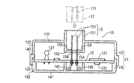
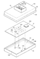
図1は、本発明の第1参考例に係る分岐接続箱の断面図であり、図2は、その分解斜視図である。これらの図において、分岐接続箱10は、合成樹脂等の可撓性材料からなるケース11と、このケース11の内部に収納された合成樹脂等の可撓性材料からなる回路基板12とを備えている。
【0016】
ケース11は、アッパーケース13とロアーケース14とを備え、後述する各開口133,143を対向させた状態で互いに嵌合させて組み合わせることにより構成したものである。アッパーケース13は、主壁131と、主壁131の周縁に一体形成された周壁132とからなる下面に開口133を有するもので、主壁131にコネクタハウジング151が一体に形成されたものである。このコネクタハウジング151は、本参考例ではその底壁152が開口133側に陥没した状態で形成されているが、その底壁152は主壁131と同じ平面内に形成されていてもよい。いずれの場合でも、底壁152は主壁131の一部を構成することになる。
【0017】
また、コネクタハウジング151の底壁152(すなわち、主壁131)に、金属板を打ち抜く等して形成された長尺状の複数の雄型のコネクタ端子153が一端側をコネクタハウジング151内におけるケース11外部に位置させ、他端側をケース11内部に位置させた状態で固設されている。このコネクタ端子153の底壁152における固設は、本参考例では底壁152に形成されたコネクタ端子153の横断面よりも僅かに小さい断面を有する貫通孔154に圧入する等して行われる。また、コネクタ端子153には幅広の鍔部155が形成されており、この鍔部155が貫通孔154に圧入されることにより軸方向における位置決めが行われるようになっている。これらのコネクタハウジング151とコネクタ端子153とでコネクタ15がケース11に一体に構成される。
【0018】
ロアーケース14は、主壁141と、主壁141の周縁に一体形成された周壁142とからなる上面に開口143を有するもので、この開口143の内周縁に回路基板12を載置するための段部144が形成され、ロアーケース14内における主壁141には段部144の位置にまで伸びる複数(本参考例では4つ)の撓み阻止手段であるロッド状の突起145が一体成型により形成されている。
【0019】
回路基板12は、所定の図略の配線導体が配設され、チップタイプやリード線タイプの複数の電子部品121が配線導体に半田等で接続されて搭載される一方、アッパーケース13に固設されたコネクタ端子153の他端が挿入される複数の貫通孔122が形成されると共に、貫通孔122の各周囲には配線導体に接続された図略のランドが形成されており、各貫通孔122に挿入されたコネクタ端子153の他端が半田等で接続されて各ランドに固着されている。上記複数の突起145は、各コネクタ端子153の回路基板12における複数の固着部を取り囲む位置であってその固着部の近傍位置に当接するような位置に形成されている。
【0020】
このような構成になる分岐接続箱10は、アッパーケース13に支持されたコネクタ端子153の他端を回路基板12の貫通孔122に挿通して半田等で固着し、その後にアッパーケース13の開口133とロアーケース14の開口143とを嵌合させ、ねじ止めや係合等の適宜の固定手段により一体化することにより組み立てられることになる。このとき、回路基板12は、ロアーケース14の段部144と突起145とに当接され、これによりケース11内に固定された状態となる。
【0021】
このように構成された分岐接続箱10では、コネクタハウジング151内に外部コネクタ17を装着して雌型のコネクタ端子171を雄型のコネクタ端子153に圧入するときにアッパーケース13が回路基板12側に押圧された状態になっても、回路基板12はロアーケース14に形成された突起145に当接されて撓まないようになるので、コネクタ端子153の回路基板12における固着部にストレスが生じないようになる。このため、固着部に亀裂が生じたり、ランドが剥離して断線状態になったりすることがなく、また、回路基板12に搭載されている電子部品121の回路基板12に対する電気接続が絶たれたり、電子部品121自体が破壊されたりすることもなくなる。
【0022】
なお、突起145は、本参考例ではコネクタ端子153の回路基板12における固着部近傍に当接する位置に形成されているが、その固着部から所定距離だけ離間した位置に形成することも可能である。但し、固着部から離間しすぎると回路基板12が撓み易くなるため、回路基板12の材料種別や厚さ等によって定まる撓みの程度により離間可能な距離が決まることになる。
【0023】
また、突起145は、本参考例ではロアーケース14との一体成型により形成されたものであるが、合成樹脂やセラミック等の絶縁材料で別個に形成したものを接着剤により固着したり、螺合手段で固着したりするようにしてもよい。いずれの場合でも、ロアーケース14に一体に形成することにより突起145を所定の長さのものとすることができる結果、回路基板12を突起145に確実に当接させることができるようになり、回路基板12の撓みを効果的に阻止することができる。
【0024】
また、突起145は、アッパーケース13に回路基板12側への押圧力が加えられていない状態において回路基板12から僅かに離間するような長さに形成されていてもよい。この場合でも、アッパーケース13に押圧力が加えられた状態では回路基板12が突起145に直ちに当接することになり、回路基板12の撓みを効果的に阻止することができる。
【0025】
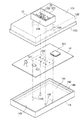
図3は、本発明の第2参考例に係る分岐接続箱の縦断面図であり、図4は、その分解斜視図である。これらの図において、第1参考例と同一の構成部材には同一の参照符号を付すことによりその詳細な説明を省略し、以下には第1参考例との相違点を中心に説明する。すなわち、この第2参考例に係る分岐接続箱10´は、アッパーケース13とロアーケース14とからなるケース11と、このケース11の内部に固定された状態で収納された回路基板12とを備えており、アッパーケース13内におけるコネクタハウジング151の底壁152(すなわち、主壁131)であってロアーケース14に形成された各突起145(以下、第1突起145という。)に対応する位置に、回路基板12に当接する位置にまで伸びる複数(本参考例では4つ)の撓み阻止手段であるロッド状の第2突起134が一体成型により形成されたものである。
【0026】
このように構成された分岐接続箱10´では、コネクタ端子153に外部コネクタ端子171を圧入するときにアッパーケース13が回路基板12側に押圧された状態になっても、第1突起145と第2突起134とが回路基板12を介して互いに当接することからケース撓みが阻止されて回路基板12が撓まないようになる。このため、コネクタ端子153の回路基板12における固着部にストレスが生じないようになり、固着部に亀裂が生じたり、ランドが剥離して断線状態になったりすることがなく、また、回路基板12に搭載されている電子部品121の回路基板12に対する電気接続が絶たれたり、電子部品121自体が破壊されたりすることもなくなる。
【0027】
また、このように構成された分岐接続箱10´では、コネクタ端子153から外部コネクタ端子171を引き抜くときにアッパーケース13が回路基板12から離反する方向に引っ張られた状態になったとしても、回路基板12が第2突起134に当接することによって回路基板12の撓みが阻止されるので、回路基板12が撓むことにより生じる不都合が生じないことになる。
【0028】
なお、第2突起134は、本参考例では第1突起145に対応する位置に形成されているが、第1突起145から回路基板12の面方向にずれた位置に形成されていてもよい。この場合でも、第2突起134は第1突起145に支持された回路基板12に当接することからケース撓みが阻止されて回路基板12が撓まないようになる。また、第1突起145及び第2突起134は、コネクタ端子153の回路基板12における固着部近傍に当接する位置に形成されているが、その固着部から所定距離だけ離間した位置に形成することも可能である。但し、固着部から離間しすぎると回路基板12が撓み易くなるため、回路基板12の材料種別や厚さ等によって定まる撓みの程度により離間可能な距離が決まることになる。
【0029】
また、第2突起134は、本参考例ではアッパーケース13との一体成型により形成されたものであるが、合成樹脂やセラミック等の絶縁材料で別個に形成したものを接着剤や螺合手段等で固着するようにしてもよい。いずれの場合でも、アッパーケース13に一体に形成することにより第2突起134を所定の長さのものとすることができるため、第2突起134を回路基板12に確実に当接させることができ、ケース撓みを効果的に阻止することができる。
【0030】
また、第2突起134は、アッパーケース13に回路基板12側への押圧力が加えられていない状態において回路基板12から僅かに離間するような長さに形成されていてもよい。この場合でも、アッパーケース13に押圧力が加えられた状態では第2突起134に回路基板12に直ちに当接することになり、アッパーケース13の撓みを効果的に阻止することができる。
【0031】
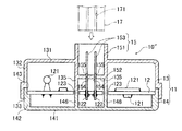
図5は、本発明の一実施形態に係る分岐接続箱の縦断面図であり、図6は、その分解斜視図である。これらの図において、第1参考例と同一の構成部材には同一の参照符号を付すことによりその詳細な説明を省略し、以下には第1参考例との相違点を中心に説明する。すなわち、この実施形態に係る分岐接続箱10″は、アッパーケース13とロアーケース14とからなるケース11と、このケース11の内部に固定された状態で収納された回路基板12とを備えている。アッパーケース13内には、コネクタハウジング151の底壁152(すなわち、主壁131)に回路基板12側に伸びる複数(本実施形態では4つ)の撓み阻止手段であるロッド状の突起135が一体成型により形成され、ロアーケース14内には、突起135に対応する位置に回路基板12側に伸びる複数(本実施形態では4つ)の撓み阻止手段であるロッド状の突起146が一体成型により形成されている。
【0032】
これらの突起135,146は、コネクタ端子136の回路基板12における複数の固着部を取り囲む位置であって、その固着部の近傍位置に当接するような位置に形成されており、回路基板12に穿設された貫通孔123を介して互いに当接されるようになっている。なお、貫通孔123は、突起135,146の横断面よりも大きな径で形成されており、回路基板12に位置ずれ等が生じた場合でも突起135,146が当接可能にされている。
【0033】
このように構成された分岐接続箱10″では、コネクタ端子153に外部コネクタ端子171を圧入するときにアッパーケース13が回路基板12側に押圧された状態になっても、両突起135,146が回路基板12の貫通孔123を介して互いに当接することからケース撓みが阻止されて回路基板12が撓まないようになる。このため、コネクタ端子153の回路基板12における固着部にストレスが生じないようになり、固着部に亀裂が生じたり、ランドが剥離して断線状態になったりすることがなくなる一方、回路基板12に搭載されている電子部品の回路基板に対する電気接続が絶たれたり、電子部品自体が破壊されたりすることもなくなる。
【0034】
なお、両突起135,146は、本実施形態ではコネクタ端子153の回路基板12における固着部近傍に当接する位置に形成されているが、その固着部から所定距離だけ離間した位置に形成することも可能である。但し、固着部から離間しすぎると回路基板12が撓み易くなるため、回路基板12の材料種別や厚さ等によって定まる撓みの程度により離間可能な距離が決まることになる。
【0035】
また、本実施形態では突起135はアッパーケース13との一体成型により形成されたものであり、突起146はロアーケース14との一体成型により形成されたものであるが、合成樹脂やセラミック等の絶縁材料で別個に形成したものを接着剤や螺合手段等で固着するようにしてもよい。いずれの場合でも、アッパーケース13及びロアーケース14に一体に形成することにより突起135,146を所定の長さのものとすることができる結果、両者を確実に当接させることができるようになり、ケース撓みを効果的に阻止することができる。
【0036】
また、両突起135,146は、アッパーケース13に回路基板12側への押圧力が加えられていない状態において僅かに離間するような長さに形成されていてもよい。この場合でも、アッパーケース13に押圧力が加えられた状態では両突起135,146は直ちに互いに当接することになり、アッパーケース13の撓みを効果的に阻止することができる。
【0037】
また、上記のいずれの参考例及び実施形態においても、アッパーケース13に固設されたコネクタ端子153は雄型のものであるが、雌型のものとすることも可能である。この場合は、外部コネクタ17のコネクタ端子171は雄型のものとなる。また、上記のいずれの参考例及び実施形態においても、アッパーケース13及びロアーケース14は開口を有する凹状に形成されたものであるが、いずれか一方を板状のものとしてもよい。要は、アッパーケース13とロアーケース14とを組み合わせて1つのケースが構成されるようになっておればよい。また、上記参考例及び実施形態における突起134、135,145,146は、いずれもロッド状のものを4つ形成するようにしているが、その形状や本数等は任意に設定することができる。さらに、本発明に係る分岐接続箱は、ケース11内にバスバー基板等を収納する等して自動車用ジャンクションボックスとすることも可能である。
【0038】
【発明の効果】
以上説明したように、請求項1の発明では、第1ケース部材に回路基板側に伸びるように形成された複数の突起と、第2ケース部材に回路基板側に伸びるように形成された複数 の突起とからなり、これら第1ケース部材の突起と第2ケース部材の突起とが回路基板に穿設された貫通孔を介して互いに当接するようにされてなる撓み阻止手段を設けているので、コネクタ端子に外部コネクタ端子を圧入するときに生じるケース撓みが確実に阻止され、回路基板が撓まないようになる分岐接続箱を実現することができる。
【0039】
また、請求項2に係る発明では、第1ケース部材の突起及び第2ケース部材の突起はコネクタ端子の回路基板における固着部近傍位置で互いに当接するように形成されているので、第1ケース部材の突起と第2ケース部材の突起とが第1,第2ケース部材の開口面方向における狭い範囲内で互いに当接されることからケース撓みが確実に阻止され、回路基板が撓まないようになる分岐接続箱を実現することができる。
【0040】
また、請求項3に係る発明では、コネクタ端子はコネクタハウジングの底壁に固設されたものであり、第1ケース部材の突起はコネクタハウジングの底壁に形成されているので、第1ケース部材に形成されたコネクタハウジングの底壁の突起と第2ケース部材の突起とが第1,第2ケース部材の開口面方向における狭い範囲内で互いに当接されることからケース撓みが確実に阻止され、回路基板が撓まないようになる分岐接続箱を実現することができる。
【0041】
また、請求項4に係る発明では、回路基板に穿設された貫通孔が、第1ケース部材の突起及び第2ケース部材の突起の横断面よりも大きな径を有しているので、回路基板が位置ずれした状態でケースに固定された場合であっても、第1,第2ケース部材の突起が回路基板に穿設された貫通孔を介して確実に当接することになり、ケース撓みが確実に阻止され、回路基板が撓まないようになる分岐接続箱を実現することができる。
【図面の簡単な説明】
【図1】 本発明の第1参考例に係る分岐接続箱の縦断面図である。
【図2】 図1に示す分岐接続箱の分解斜視図である。
【図3】 本発明の第2参考例に係る分岐接続箱の縦断面図である。
【図4】 図3に示す分岐接続箱の分解斜視図である。
【図5】 本発明の一実施形態に係る分岐接続箱の縦断面図である。
【図6】 図5に示す分岐接続箱の分解斜視図である。
【図7】 従来例の分岐接続箱の縦断面図である。
【符号の説明】
10,10´,10″ 分岐接続箱
11 ケース
12 回路基板
13 アッパーケース(第1ケース部材)
14 ロアーケース(第2ケース部材)
15 コネクタ
17 外部コネクタ
123 貫通孔
134 第2突起
135,146 突起
145 突起(第1突起)
151 コネクタハウジング
153 コネクタ端子
171 外部コネクタ端子[0001]
BACKGROUND OF THE INVENTION
The present invention relates to a branch connection box in which a connector is integrally formed in a case in which a circuit board is accommodated.
[0002]
[Prior art]
Conventionally, this type of junction box is a case made of a flexible material such as a synthetic resin composed of an
[0003]
The branch junction box configured as described above is used, for example, for branch connection of a wire harness of an automobile. An
[0004]
[Problems to be solved by the invention]
By the way, in the above conventional junction box, when the
[0005]
In order to solve such a problem, as described in Japanese Patent Laid-Open No. 9-186475, it is conceivable to extend the tip of the
[0006]
The present invention has been made in view of such circumstances, and an object of the present invention is to provide a branch connection box that can surely prevent case bending that occurs when an external connector terminal is press-fitted into a connector terminal.
[0007]
[Means for Solving the Problems]
In order to achieve the above object, the invention according to claim 1 is directed to a case constituted by a first case member and a second case member whose openings are opposed to each other, with a circuit board facing the first case member. In a state in which the other surface is fixed to be opposed to the second case member, and a plurality of connector terminals are located at one end side outside the case and at the other end side inside the case. In the branch connection box, which is fixedly provided and each other end of the connector terminal is fixed to the circuit board, case bending that occurs when an external connector terminal is press-fitted into the connector terminal is prevented . A plurality of protrusions formed on the case member so as to extend toward the circuit board; and a plurality of protrusions formed on the second case member so as to extend toward the circuit board. Is characterized in that the projection of the force and the second case member is provided with blocking means deflection formed by such contact with each other via a drilled through-hole in the circuit board.
[0008]
According to this configuration, the protrusions of the first case member and the protrusions of the second case member are brought into contact with each other through the through holes formed in the circuit board. When the connector terminal of the external connector is pressed into the connector terminal, even if the case is pressed to the circuit board side, the case bending is effectively prevented, and unnecessary pressing force does not act on the circuit board. The For this reason, as a result of the circuit board not being bent, stress is not generated in the fixing portion of the connector terminal on the circuit board, the fixing portion is cracked, or the land is peeled off to be disconnected. Is effectively prevented. In addition, since the circuit board does not bend, it is possible to effectively prevent the electrical connection of the electronic component to the circuit board and the destruction of the electronic component itself.
[0009]
According to a second aspect of the present invention, in the first aspect, the protrusion of the first case member and the protrusion of the second case member abut each other at a position near the fixing portion of the circuit board of the connector terminal. It is characterized by being formed as follows.
[0010]
According to this configuration, the protrusion of the first case member and the protrusion of the second case member are brought into contact with each other within a narrow range in the opening surface direction of the first case member and the second case member. deflection is reliably prevented, ing so does not flex circuit board.
[0011]
The invention according to claim 3 is the one according to claim 2, wherein a connector housing is formed on the first case member, and the connector terminal is fixed to a bottom wall of the connector housing, projections of the first case member is characterized that you have formed in the bottom wall of the connector housing.
[0012]
According to this configuration, the protrusion on the bottom wall of the connector housing formed on the first case member and the protrusion on the second case member are in contact with each other within a narrow range in the opening surface direction of the first case member and the second case member. the results will be contact, case deflection is reliably prevented, ing so does not flex circuit board.
[0013]
According to a fourth aspect of the invention, there is provided the method according to any one of the first to third aspects, wherein the through-hole formed in the circuit board includes a protrusion of the first case member and a protrusion of the second case member. It is characterized that you have has a larger diameter than the cross-section.
[0014]
According to this configuration, even when the circuit board is fixed to the case in a misaligned state, the protrusions of the first case member and the protrusions of the second case member have the through holes formed in the circuit board. result that will reliably abut through the case deflection is reliably prevented, ing so does not flex circuit board.
[0015]
DETAILED DESCRIPTION OF THE INVENTION
FIG. 1 is a sectional view of a branch junction box according to a first reference example of the present invention, and FIG. 2 is an exploded perspective view thereof. In these drawings, the
[0016]
The
[0017]
In addition, a plurality of long
[0018]
The
[0019]
The
[0020]
The
[0021]
In the
[0022]
In this reference example , the
[0023]
In addition, the
[0024]
Further, the
[0025]
FIG. 3 is a longitudinal sectional view of a branch junction box according to a second reference example of the present invention, and FIG. 4 is an exploded perspective view thereof. In these drawings, the same components as those in the first reference example are denoted by the same reference numerals, and a detailed description thereof will be omitted. Hereinafter, differences from the first reference example will be mainly described. That is, the
[0026]
In the
[0027]
Further, in the branched
[0028]
The
[0029]
The
[0030]
Further, the
[0031]
FIG. 5 is a longitudinal cross-sectional view of a branch junction box according to an embodiment of the present invention, and FIG. 6 is an exploded perspective view thereof. In these drawings, the same components as those in the first reference example are denoted by the same reference numerals, and a detailed description thereof will be omitted. Hereinafter, differences from the first reference example will be mainly described. That is, the branch
[0032]
These
[0033]
In the thus configured branch
[0034]
Incidentally, both the
[0035]
Further, in this embodiment, the
[0036]
Further, both the
[0037]
Further, in any of the above reference examples and embodiments, the
[0038]
【The invention's effect】
As described above, in the first aspect of the invention, the plurality of protrusions formed on the first case member so as to extend toward the circuit board side, and the plurality of protrusions formed on the second case member so as to extend toward the circuit board side . Since the protrusions of the first case member and the protrusions of the second case member are provided with the protrusions, the bending prevention means is provided so as to come into contact with each other through a through hole formed in the circuit board. deflection case occurs when press-fitting the external connector terminal to the connector terminal is reliably prevented, it is possible to realize a branch joint box ing so does not flex circuit board.
[0039]
In the invention according to claim 2, since the protrusion of the first case member and the protrusion of the second case member are formed so as to contact each other at a position near the fixing portion of the circuit board of the connector terminal , the first case member The protrusions of the second case member and the protrusions of the second case member are in contact with each other within a narrow range in the opening surface direction of the first and second case members, so that the case bending is reliably prevented and the circuit board does not bend. A branch junction box can be realized.
[0040]
In the invention according to claim 3, the connector terminal is fixed to the bottom wall of the connector housing, and the projection of the first case member is formed on the bottom wall of the connector housing. Since the protrusion on the bottom wall of the connector housing and the protrusion on the second case member formed on each other are in contact with each other within a narrow range in the opening surface direction of the first and second case members, the case bending is reliably prevented. , it is possible to realize a branch joint box ing so does not flex circuit board.
[0041]
In the invention according to claim 4, since the through hole formed in the circuit board has a larger diameter than the cross section of the protrusion of the first case member and the protrusion of the second case member, Even when the case is fixed to the case in a misaligned state, the projections of the first and second case members are surely brought into contact with each other through the through holes formed in the circuit board, and the case is bent. is reliably prevented, it is possible to realize a branch joint box ing so does not flex circuit board.
[Brief description of the drawings]
FIG. 1 is a longitudinal sectional view of a junction box according to a first reference example of the present invention.
FIG. 2 is an exploded perspective view of the branch connection box shown in FIG.
FIG. 3 is a longitudinal sectional view of a branch junction box according to a second reference example of the present invention.
4 is an exploded perspective view of the branch connection box shown in FIG. 3. FIG.
FIG. 5 is a longitudinal sectional view of a junction box according to an embodiment of the present invention.
6 is an exploded perspective view of the branch connection box shown in FIG. 5. FIG.
FIG. 7 is a longitudinal sectional view of a branch junction box of a conventional example.
[Explanation of symbols]
10, 10 ′, 10 ″
14 Lower case (second case member)
15
Claims (4)
Priority Applications (3)
| Application Number | Priority Date | Filing Date | Title |
|---|---|---|---|
| JP06700899A JP3673422B2 (en) | 1999-03-12 | 1999-03-12 | Branch connection box |
| EP20000105085 EP1034983B1 (en) | 1999-03-12 | 2000-03-10 | Branch connection box |
| DE2000604418 DE60004418T2 (en) | 1999-03-12 | 2000-03-10 | A branch junction box |
Applications Claiming Priority (1)
| Application Number | Priority Date | Filing Date | Title |
|---|---|---|---|
| JP06700899A JP3673422B2 (en) | 1999-03-12 | 1999-03-12 | Branch connection box |
Publications (2)
| Publication Number | Publication Date |
|---|---|
| JP2000261160A JP2000261160A (en) | 2000-09-22 |
| JP3673422B2 true JP3673422B2 (en) | 2005-07-20 |
Family
ID=13332477
Family Applications (1)
| Application Number | Title | Priority Date | Filing Date |
|---|---|---|---|
| JP06700899A Expired - Fee Related JP3673422B2 (en) | 1999-03-12 | 1999-03-12 | Branch connection box |
Country Status (3)
| Country | Link |
|---|---|
| EP (1) | EP1034983B1 (en) |
| JP (1) | JP3673422B2 (en) |
| DE (1) | DE60004418T2 (en) |
Cited By (1)
| Publication number | Priority date | Publication date | Assignee | Title |
|---|---|---|---|---|
| US9585253B2 (en) | 2015-03-05 | 2017-02-28 | Denso Corporation | Electronic device |
Families Citing this family (36)
| Publication number | Priority date | Publication date | Assignee | Title |
|---|---|---|---|---|
| JP2000294961A (en) * | 1999-04-01 | 2000-10-20 | Harness Syst Tech Res Ltd | Joint box case and joint box assembling method |
| US20060077640A1 (en) * | 2002-05-14 | 2006-04-13 | Sumitomo Electric Industries, Ltd. | Optical module |
| JP2004247700A (en) * | 2002-05-14 | 2004-09-02 | Sumitomo Electric Ind Ltd | Optical module |
| US6752632B1 (en) * | 2003-03-21 | 2004-06-22 | The Boeing Company | Connector interface pad for structurally integrated wiring |
| US6683789B1 (en) * | 2003-04-28 | 2004-01-27 | Motorola, Inc. | Electronic control module for a removable connector and methods of assembling same |
| JP2005130633A (en) * | 2003-10-24 | 2005-05-19 | Yazaki Corp | Electrical junction box |
| KR101108050B1 (en) * | 2004-11-10 | 2012-01-25 | 엘지전자 주식회사 | Remote monitor device of home appliance |
| JP2006331803A (en) * | 2005-05-25 | 2006-12-07 | Denso Corp | Electronic control device |
| DE102008040157A1 (en) * | 2008-07-03 | 2010-01-07 | Robert Bosch Gmbh | Personal protective device for a vehicle or method for assembling such a control device |
| JP2010251644A (en) * | 2009-04-20 | 2010-11-04 | Denso Wave Inc | Security device |
| JP5587152B2 (en) * | 2010-11-30 | 2014-09-10 | 住友電装株式会社 | Electrical junction box |
| WO2013008632A1 (en) * | 2011-07-11 | 2013-01-17 | 日本電気株式会社 | Piezoelectric vibration sensor |
| KR101772490B1 (en) | 2011-09-28 | 2017-08-30 | 삼성전자주식회사 | Printed circuit board assembly |
| JP6021623B2 (en) * | 2012-12-11 | 2016-11-09 | 三菱重工業株式会社 | Inverter-integrated electric compressor |
| JP2014154474A (en) * | 2013-02-13 | 2014-08-25 | Panasonic Corp | Usb receptacle |
| JP6029484B2 (en) * | 2013-02-20 | 2016-11-24 | 三菱重工オートモーティブサーマルシステムズ株式会社 | Inverter-integrated electric compressor |
| JP6096003B2 (en) * | 2013-02-21 | 2017-03-15 | 三菱重工オートモーティブサーマルシステムズ株式会社 | Inverter-integrated electric compressor |
| DE102013003800A1 (en) * | 2013-03-05 | 2014-09-11 | Wabco Gmbh | Housing for receiving a printed circuit board with at least one connector interface, electronic module with such housing, motor vehicle and method for producing such a housing or electronic module |
| JP6153745B2 (en) * | 2013-03-07 | 2017-06-28 | 三菱重工オートモーティブサーマルシステムズ株式会社 | Inverter board and inverter-integrated electric compressor using the same |
| JP6173763B2 (en) * | 2013-04-26 | 2017-08-02 | 三菱重工オートモーティブサーマルシステムズ株式会社 | Inverter-integrated electric compressor |
| DE102014205744B4 (en) | 2014-01-24 | 2019-05-29 | Eberspächer Climate Control Systems GmbH & Co. KG | Control unit for a vehicle heater |
| KR101636288B1 (en) * | 2014-12-23 | 2016-07-06 | 주식회사 유라코퍼레이션 | Junction box |
| JP6544181B2 (en) * | 2015-09-29 | 2019-07-17 | 株式会社デンソー | Electronic control unit |
| JP6542642B2 (en) * | 2015-11-11 | 2019-07-10 | 日立オートモティブシステムズ株式会社 | Electronic control unit |
| JP6827212B2 (en) * | 2016-12-20 | 2021-02-10 | パナソニックIpマネジメント株式会社 | Sensor device and lighting equipment |
| JP6890275B2 (en) * | 2017-07-20 | 2021-06-18 | パナソニックIpマネジメント株式会社 | USB outlet |
| JP7081250B2 (en) * | 2018-03-22 | 2022-06-07 | 株式会社デンソー | Power converter |
| JP7076265B2 (en) * | 2018-04-03 | 2022-05-27 | スリーエム イノベイティブ プロパティズ カンパニー | connector |
| JP6871230B2 (en) * | 2018-12-28 | 2021-05-12 | 矢崎総業株式会社 | Electrical junction box |
| KR102151781B1 (en) * | 2019-03-07 | 2020-09-03 | 엘에스일렉트릭(주) | Structure for supporting PCB |
| JP7289107B2 (en) * | 2019-03-11 | 2023-06-09 | パナソニックIpマネジメント株式会社 | USB outlet |
| JP7317689B2 (en) * | 2019-12-20 | 2023-07-31 | 矢崎総業株式会社 | Electrical junction box, wire harness, and electrical junction box manufacturing method |
| JP7378897B2 (en) * | 2019-12-20 | 2023-11-14 | 矢崎総業株式会社 | Electrical junction box and wire harness |
| JP2020113790A (en) * | 2020-04-03 | 2020-07-27 | パナソニックIpマネジメント株式会社 | USB outlet |
| KR102518754B1 (en) * | 2021-04-07 | 2023-04-06 | 주식회사 경신 | Junction-box of vehicle |
| JP7732867B2 (en) * | 2021-11-18 | 2025-09-02 | 矢崎総業株式会社 | Electrical connectors and electrical junction boxes |
Family Cites Families (4)
| Publication number | Priority date | Publication date | Assignee | Title |
|---|---|---|---|---|
| JPS6261856A (en) * | 1985-09-12 | 1987-03-18 | Yazaki Corp | Wiring device assembled with functions for automobile |
| JPH0614475B2 (en) * | 1989-06-09 | 1994-02-23 | 矢崎総業株式会社 | Connection structure of bus bar and insulation displacement terminal for branch in electric junction box |
| DE3936906C2 (en) * | 1989-11-06 | 1995-02-02 | Telefunken Microelectron | Housing for automotive electronics |
| JP3405249B2 (en) * | 1999-02-01 | 2003-05-12 | 住友電装株式会社 | Electrical junction box |
-
1999
- 1999-03-12 JP JP06700899A patent/JP3673422B2/en not_active Expired - Fee Related
-
2000
- 2000-03-10 DE DE2000604418 patent/DE60004418T2/en not_active Expired - Lifetime
- 2000-03-10 EP EP20000105085 patent/EP1034983B1/en not_active Expired - Lifetime
Cited By (1)
| Publication number | Priority date | Publication date | Assignee | Title |
|---|---|---|---|---|
| US9585253B2 (en) | 2015-03-05 | 2017-02-28 | Denso Corporation | Electronic device |
Also Published As
| Publication number | Publication date |
|---|---|
| EP1034983B1 (en) | 2003-08-13 |
| DE60004418D1 (en) | 2003-09-18 |
| DE60004418T2 (en) | 2004-03-11 |
| EP1034983A3 (en) | 2001-05-16 |
| EP1034983A2 (en) | 2000-09-13 |
| JP2000261160A (en) | 2000-09-22 |
Similar Documents
| Publication | Publication Date | Title |
|---|---|---|
| JP3673422B2 (en) | Branch connection box | |
| JPH08339861A (en) | Connector socket | |
| US20090011623A1 (en) | Low profile board-mounted connector | |
| JPH0676894A (en) | Connector | |
| JPH10189181A (en) | Plug connector | |
| KR960706701A (en) | CONNECTOR FOR HIGH DENSITY ELECTRONIC ASSEMBLIES | |
| JP2005129275A (en) | Connector fixing structure | |
| EP1122825B1 (en) | Substrate mount type terminal | |
| JP3607241B2 (en) | Electrical connector | |
| US6899565B2 (en) | Electrical connector having a holddown for ground connection | |
| JPH10302862A (en) | Electrical connector | |
| KR20010080773A (en) | Device for electrically and mechanically connecting two printed circuit boards | |
| US6340321B2 (en) | Electrical connector | |
| JP2921248B2 (en) | connector | |
| US7303408B2 (en) | Connector | |
| JP4414845B2 (en) | connector | |
| KR102686427B1 (en) | Interposer Unit For Floating Board to Board Connector | |
| JP5922325B2 (en) | Circuit board electrical connector | |
| JP4861055B2 (en) | connector | |
| JPH0126064Y2 (en) | ||
| JP2005019053A (en) | Electrical connector | |
| JPH06231840A (en) | Connector and connector mounting fixture | |
| JPH0461773A (en) | Structure of connector mounting part | |
| JPH034469A (en) | Structure of connectors in electronic equipment | |
| JP3289207B2 (en) | Electrical connectors mounted on printed circuit boards |
Legal Events
| Date | Code | Title | Description |
|---|---|---|---|
| A131 | Notification of reasons for refusal |
Free format text: JAPANESE INTERMEDIATE CODE: A131 Effective date: 20041102 |
|
| A521 | Written amendment |
Free format text: JAPANESE INTERMEDIATE CODE: A523 Effective date: 20041228 |
|
| TRDD | Decision of grant or rejection written | ||
| A01 | Written decision to grant a patent or to grant a registration (utility model) |
Free format text: JAPANESE INTERMEDIATE CODE: A01 Effective date: 20050419 |
|
| A61 | First payment of annual fees (during grant procedure) |
Free format text: JAPANESE INTERMEDIATE CODE: A61 Effective date: 20050422 |
|
| R150 | Certificate of patent or registration of utility model |
Free format text: JAPANESE INTERMEDIATE CODE: R150 |
|
| FPAY | Renewal fee payment (event date is renewal date of database) |
Free format text: PAYMENT UNTIL: 20080428 Year of fee payment: 3 |
|
| FPAY | Renewal fee payment (event date is renewal date of database) |
Free format text: PAYMENT UNTIL: 20090428 Year of fee payment: 4 |
|
| FPAY | Renewal fee payment (event date is renewal date of database) |
Free format text: PAYMENT UNTIL: 20100428 Year of fee payment: 5 |
|
| FPAY | Renewal fee payment (event date is renewal date of database) |
Free format text: PAYMENT UNTIL: 20110428 Year of fee payment: 6 |
|
| FPAY | Renewal fee payment (event date is renewal date of database) |
Free format text: PAYMENT UNTIL: 20110428 Year of fee payment: 6 |
|
| FPAY | Renewal fee payment (event date is renewal date of database) |
Free format text: PAYMENT UNTIL: 20120428 Year of fee payment: 7 |
|
| FPAY | Renewal fee payment (event date is renewal date of database) |
Free format text: PAYMENT UNTIL: 20130428 Year of fee payment: 8 |
|
| FPAY | Renewal fee payment (event date is renewal date of database) |
Free format text: PAYMENT UNTIL: 20140428 Year of fee payment: 9 |
|
| LAPS | Cancellation because of no payment of annual fees |