JP3672452B2 - Power supply circuit and power supply device using the same - Google Patents
Power supply circuit and power supply device using the same Download PDFInfo
- Publication number
- JP3672452B2 JP3672452B2 JP08036099A JP8036099A JP3672452B2 JP 3672452 B2 JP3672452 B2 JP 3672452B2 JP 08036099 A JP08036099 A JP 08036099A JP 8036099 A JP8036099 A JP 8036099A JP 3672452 B2 JP3672452 B2 JP 3672452B2
- Authority
- JP
- Japan
- Prior art keywords
- capacitor
- power supply
- circuit
- voltage
- full
- Prior art date
- Legal status (The legal status is an assumption and is not a legal conclusion. Google has not performed a legal analysis and makes no representation as to the accuracy of the status listed.)
- Expired - Fee Related
Links
Images

Landscapes
- Rectifiers (AREA)
- Dc-Dc Converters (AREA)
Description
【0001】
【発明の属する技術分野】
本発明は交流電力を受電し、各種負荷に直流電力を供給する電源回路およびそれを用いた電源装置に関する。
【0002】
【従来の技術】
近年、電子機器に対する省エネルギー化の社会的要望が高くなっている。特に、ビデオテープレコーダ(VTR)、複写機、ファクシミリ等のように終日通電状態にあり、運転モードに比べて待機モードが長く継続する電子機器に対して、省エネルギー化を図るため待機モードでの低消費電力化が進められている。このような電子機器における低消費電力化はもちろんであるが、電子機器に電力を供給する電源装置の待機モードでのエネルギーの低損失化も進められている。
また、近年、電子機器が複雑になるにしたがって、精度の高い直流電力を供給する必要が増大している。精度の高い直流電力を供給できる電源装置は、パソコン、ファクシミリ、携帯電話機、コピー機などの情報通信機器などに用いられている。
【0003】
以下、従来の電源装置について図2を参照して具体的に説明する。図2は従来のスイッチング電源装置の回路構成を示す回路図である。
図2において、交流電源100は、交流電力を全波整流回路20へ供給する。全波整流回路20と入力コンデンサ30は、交流電源100からの交流電圧を直流電圧に整流し平滑化する。
スイッチング回路40は、スイッチングトランジスタやパワーMOSFETのような素子により構成され、入力された直流電圧をオンオフ動作により高周波交流電圧に変換する。トランス50は1次巻線50aと2次巻線50bと制御巻線50cとを有している。スイッチング回路40において、スイッチング動作により得られた高周波交流電圧はトランス50の1次巻線50aに入力される。
【0004】
トランス50の2次巻線50bに接続されたダイオード60と出力コンデンサ70は、2次巻線50bに発生した交流電圧を整流平滑し、負荷80へ直流電力を供給する。制御駆動回路90は、負荷80へ出力される直流電力を調整するスイッチング回路40を制御している。トランス50の制御巻線50cに接続されているダイオード250及びコンデンサ110は、制御巻線50cに発生する交流電圧を整流平滑して、制御駆動回路90の電源として供給する。抵抗31は起動抵抗であり、トランス50の各巻線に電圧が生じていない起動時において制御駆動回路90に電力を供給する。
【0005】
以下、従来の電源装置における動作について説明する。
交流電源100は、交流電力を全波整流回路20へ供給する。全波整流回路20と入力コンデンサ30は、交流電源100の交流電圧を直流電圧に全波整流し平滑化する。
スイッチング回路40は、そのオンオフ動作により直流電圧を高周波交流電圧に変換する。この高周波交流電圧はトランス50の1次巻線50aに入力され2次巻線50bから変圧されて出力される。2次巻線50bに発生する高周波交流電圧は、ダイオード60及び出力コンデンサ70により整流平滑されて直流電圧が形成される。この直流電圧は負荷80に供給される。負荷80に供給される直流電圧はスイッチング回路40のオンオフ比により調整される。
【0006】
制御駆動回路90は、出力された直流電圧を検知して基準電圧と比較し、誤差を検出する。制御駆動回路90はその誤差を補正するよう調整したオンオフ比のパルス信号をスイッチング回路40へ出力する。
制御巻線50cに発生する交流電圧は、ダイオード250及びコンデンサ110によって整流平滑され、制御駆動回路90の電源として供給される。起動抵抗31の回路により、トランス50の各巻線に電圧の発生しない起動時において制御駆動回路90に電力が供給される。
待機モードに代表される軽負荷時において、従来の電源装置のエネルギー損失の要因の一つにこの起動抵抗31における電力損失がある。このため、起動抵抗31の抵抗値は大きくしたいところだが、従来の電源装置の起動をスムーズにするためにも、起動抵抗31の抵抗値はあまり大きくできなかった。
【0007】
上記のような構成の従来の電源装置に対して、起動抵抗を用いない電源装置用の電源回路が用いられていた。
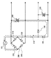
以下、起動抵抗を用いない従来の電源装置用の電源回路について図3を参照して具体的に説明する。図3は従来の電源回路の回路構成を示す回路図である。
交流電源101は、交流電力を全波整流回路200へ供給する。全波整流回路200は、4つのダイオード210,220,230,240によりブリッジに構成されている。全波整流回路200と入力コンデンサ300は、交流電源101の交流電圧を直流電圧に全波整流し平滑化している。
コンデンサ310の一端は全波整流回路200の交流側の一方の端子に接続されており、コンデンサ310の他端はダイオード140を介してコンデンサ320の正極端子に接続されている。また、コンデンサ320の負極端子はダイオード150を介してコンデンサ310の他端に接続されている。
【0008】
以下、図3に示した従来の電源装置用の電源回路の動作について説明する。
図3において、交流電源101の交流電圧は、全波整流回路200と入力コンデンサ300により直流電圧に全波整流され平滑化される。全波整流回路200に接続された交流ラインが高電位のとき、電流は交流電源101から全波整流回路200の交流ラインの一端に接続されたコンデンサ310に流れ、ダイオード140と全波整流回路200のダイオード240を介して交流電源101へ流れる。このとき、コンデンサ310とともにコンデンサ320は充電される。
逆に、全波整流回路200に接続された交流ラインが負電位に振れるとき、電流は交流電源101から全波整流回路200のダイオード220、入力コンデンサ300、ダイオード150、及びコンデンサ310に流れる。このとき、コンデンサ310に充電された電荷は放電される。この放電ループを図3において破線で示す。
以上のようにコンデンサ310が充放電動作を繰り返すことにより、コンデンサ320には交流電源101からの電力がコンデンサ310を介して供給され、充電される。
【0009】
【発明が解決しようとする課題】
図3に示した従来の電源装置用の電源回路において、コンデンサ310の接続された交流ラインが負電位に振れる時に、コンデンサ310の放電電流は入力コンデンサ300を充電する方向に流れる。
最近の電子機器における省エネルギー化に伴い、待機モードにおける軽負荷化が進んでいる。このような電子機器に図3に示した電源回路を採用した場合には、入力コンデンサ300にとっての負荷はさらに軽くなる。このため、入力コンデンサ300からの放電電力が入力コンデンサ300への充電電力より小さくなると、入力コンデンサ300の電位が異常に上昇するという問題があった。
本発明は、負荷が軽い場合であっても入力コンデンサの電位が異常に上昇することがなく、電力損失の少ない電源回路およびそれを用いた電源装置を提供することを目的とする。
【0011】
【課題を解決するための手段】
上記目的を達成するために、本発明に係る電源装置は、交流電圧を出力する交流電源、前記交流電源からの交流電圧を直流電圧に変換する全波整流平滑回路、前記全波整流平滑回路から出力された直流電圧を所定の電力形態に変換して負荷に供給するコンバータ、前記交流電源の各交流ラインにそれぞれの一端を接続された電気的特性が実質的に等しい第1のコンデンサと第2のコンデンサ、前記第1のコンデンサと第2のコンデンサのそれぞれの他端が入力側の各ラインに接続され、出力側の負極ラインが前記全波整流平滑回路の出力側の負極ラインに接続されたダイオードブリッジ構成の全波整流回路、前記ダイオードブリッジ構成の全波整流回路の出力側の各ラインに接続された第3のコンデンサ、前記第1のコンデンサと前記第2のコンデンサと前記第3のコンデンサと前記全波整流回路とを有する電源回路を起動時の電源とし、前記負荷に供給される電力形態を制御すべく前記コンバータを駆動する制御駆動回路、及び、前記コンバータの通常動作中に前記第3のコンデンサを充電し、前記制御駆動回路の電源となる電力供給回路、を具備する。
この発明によれば、極軽負荷時においても全波整流平滑回路の入力コンデンサの電位が異常に上昇することがなく、電力損失の少ない電源装置を提供することができる。また、本発明に係る電源装置は、前記第1のコンデンサと第2のコンデンサの容量が実質的に同一であり、互いの充放電電流が均衡するよう構成するとよい。
【0012】
【発明の実施の形態】
以下、本発明に係る電源回路およびそれを用いた電源装置の好適な実施例を添付の図面を参照しつつ説明する。
【0013】
《実施例1》
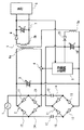
図1は本発明に係る実施例1の電源回路を用いた電源装置の回路構成を示す回路図である。
図1において、交流電源1は、ダイオード21、22、23、24のブリッジ構成からなる全波整流回路2とダイオード14、15、16、17のブリッジ構成からなる全波整流回路11へ交流電力を供給している。全波整流平滑回路は、全波整流回路2と入力コンデンサ3により構成されており、交流電源1からの交流電圧を直流電圧に変換している。
スイッチング回路4は、スイッチングトランジスタやパワーMOSFETのような素子により構成され、入力された直流電圧をオンオフ動作により高周波交流電圧に変換する。トランス5は1次巻線5aと2次巻線5bと制御巻線5cとを有している。スイッチング回路4において、スイッチング動作により得られた高周波交流電圧はトランス5の1次巻線5aに入力される。また、トランス5の2次巻線5bと制御巻線5cには絶縁して変圧された交流電圧が出力される。
【0014】
トランス5の2次巻線5bに接続されたダイオード6と出力コンデンサ7は、2次巻線5bに発生した交流電圧を整流平滑し、負荷8へ直流電力を供給する。以上のように、スイッチング回路4、トランス5、ダイオード6、及び出力コンデンサ7により、全波整流平滑回路の出力を直流電力に変換して負荷8へ供給するコンバータが構成されている。制御駆動回路9は、負荷8へ出力される直流電力を調整するスイッチング回路4を制御している。トランス5の制御巻線5cに接続されているダイオード25及び第3のコンデンサ11は、制御巻線5cに発生する交流電圧を整流平滑して、制御駆動回路9の電源として供給する。
第1のコンデンサ12と第2のコンデンサ13はそれぞれの一端が交流電源1に接続されており、同じ電気的特性を有している。ダイオード14、15、16、17でブリッジ構成された全波整流回路11の各入力端子には第1コンデンサ12と第2のコンデンサ13が接続されており、ダイオードブリッジ構成の全波整流回路11の出力端子には第3のコンデンサ10が接続され、第3のコンデンサ10を充電するよう構成されている。
【0015】
次に、実施例1の電源装置の動作について説明する。
交流電源1は、交流電力を全波整流回路2へ供給する。全波整流回路2とこの出力端子に接続された入力コンデンサ3により、交流電源1の交流電圧は全波整流されて平滑化され、直流電圧に変換される。
スイッチング回路4は、入力された直流電圧をオンオフ動作により高周波交流電圧に変換する。この高周波交流電圧はトランス5の1次巻線5aに入力され、2次巻線5bから変圧された高周波交流電圧が出力される。2次巻線5bに発生した高周波交流電圧は、ダイオード6及び出力コンデンサ7により整流平滑され、直流電圧として出力され負荷8に供給される。電源装置から出力される直流電圧は、スイッチング回路4のオンオフ比により調整される。
【0016】
制御駆動回路9は、負荷8へ供給される直流電圧を検知して、基準電圧と比較する。制御駆動回路9は検知された直流電圧と基準電圧との誤差を補正するよう調整したオンオフ比のパルス信号を出力する。
制御巻線5cに発生する交流電圧は、ダイオード25及び第3のコンデンサ10によって整流平滑され制御駆動回路9の電源となる。
【0017】
次に、実施例1の電源装置における制御駆動回路9に電源を供給する電源回路について説明する。この電源回路において、制御駆動回路9に対しては交流電源1から交流電力が以下のように供給される。
まず、第1のコンデンサ12が接続された交流ラインが高電位で上昇中のとき、電流は交流電源1→第1のコンデンサ12→ダイオード14→第3のコンデンサ10→ダイオード17→第2のコンデンサ13→交流電源1の経路で流れる。これにより、第1のコンデンサ12と第3のコンデンサ10が充電され、第2のコンデンサ13は放電する。
【0018】
次に、第1のコンデンサ12が接続された全波整流回路2の交流ラインの電位が入力コンデンサ3の電位に等しくなると、全波整流回路2が導通状態となり、入力コンデンサ3が充電される。入力コンデンサ3が充電されると同時に、電流は交流電源1→第1のコンデンサ12→ダイオード14→第3のコンデンサ10→全波整流回路2のダイオード24→交流電源1の経路で流れる。これにより、第1のコンデンサ12と第3のコンデンサ10が充電される。
次に、第1のコンデンサ12の接続された交流ラインの電位が低下し入力コンデンサ3の電位より低くなると、全波整流回路2が不導通状態となり、電流は交流電源1→第2のコンデンサ13→ダイオード16→第3のコンデンサ10→ダイオード15→第1のコンデンサ12→交流電源1の経路で流れる。これにより、第1のコンデンサ12は放電し、第2のコンデンサ13と第3のコンデンサ10は充電される。
【0019】
全波整流回路2の交流ラインの電位が反転して、交流ラインの電位が入力コンデンサ3の電位と等しくなると、全波整流回路2が導通状態となり入力コンデンサ3が充電される。入力コンデンサ3が充電されると同時に、電流は交流電源1→第2のコンデンサ13→ダイオード16→第3のコンデンサ10→全波整流回路2のダイオード23→交流電源1の経路で流れる。これにより、第2のコンデンサ13と第3のコンデンサ10は充電される。
以上の動作を繰り返すことにより、第3のコンデンサ10は交流電源1から第1コンデンサ12及び第2のコンデンサ13を介して電力供給を受ける。第1のコンデンサ12及び第2のコンデンサ13におけるそれぞれの充放電電流は互いに均衡しており、入力コンデンサ3を充電することはない。
実施例1の電源回路は上記のように動作するため、極軽負荷時において入力コンデンサ3が異常に電圧上昇することは確実に防止される。
【0020】
なお、実施例1の電源装置においては、第1のコンデンサ12、第2のコンデンサ13、第3のコンデンサ10、及びブリッジ回路11により構成された電源回路を制御駆動回路9の起動用電源として用い、通常動作時の電源にはトランス5の制御巻線5cから電力を供給する構成で説明した。しかし、本発明の電源回路は、第1のコンデンサ12、第2のコンデンサ13、第3のコンデンサ10、及びブリッジ回路11により構成された電源回路の単独でも電源回路としての機能を果たすことが可能である。この場合、第3のコンデンサ10の電圧をEc、入力電源1から供給される交流電圧のピーク値をEi、第3のコンデンサ10の負荷電流をIo、第1のコンデンサ12及び第2のコンデンサ13の静電容量を等しくC、周波数をfとすると、第3のコンデンサ10の電圧をEcは下記式(1)に示す関係を有する。
【0021】
Ec=Ei−Io/(2Cf) −−− (1)
【0022】
上記のように構成された電源回路を単独で使用する場合、第3のコンデンサ10は交流電源1から全波で充電されている。従って、半波での充電である従来の電源回路(図3)に比べて、同じ電力を供給するよう場合、第1のコンデンサ12及び第2のコンデンサ13の静電容量は半分で済み、第3のコンデンサ10の電圧Ecに重畳されるリップル電圧が小さくなる。
【0023】
【発明の効果】
以上、実施例について詳細に説明したところから明らかなように、本発明は次に効果を有する。
本発明に係る電源回路を用いた電源装置によれば、起動抵抗が不要であり、交流電源に接続された第1のコンデンサ及び第2のコンデンサにおける互いの充放電電流が均衡するよう構成されているため、入力コンデンサを充電する経路が無く、極軽負荷時において入力コンデンサが異常に電圧が上昇することがない。
また、本発明に係る電源回路によれば、従来の半波整流の電源回路に比べて、全波で電力を供給するよう構成されているため、第1のコンデンサと第2のコンデンサの静電容量を低く抑えることができ、出力電圧であるコンデンサの電圧に重畳されるリップル電圧も小さくなるという有利な効果が得られる。
【図面の簡単な説明】
【図1】本発明に係る実施例1における電源回路を用いたスイッチング電源装置の回路構成を示す回路図である。
【図2】従来のスイッチング電源装置の回路構成を示す回路図である。
【図3】従来の電源回路の回路構成を示す回路図である。
【符号の説明】
1 交流電源
2 全波整流回路
3 入力コンデンサ
4 スイッチング回路
5 トランス
6 ダイオード
7 出力コンデンサ
8 負荷
9 制御駆動回路
10 第3のコンデンサ
11 全波整流回路
12 第1のコンデンサ
13 第2のコンデンサ[0001]
BACKGROUND OF THE INVENTION
The present invention relates to a power supply circuit that receives AC power and supplies DC power to various loads, and a power supply device using the power supply circuit.
[0002]
[Prior art]
In recent years, there has been an increasing social demand for energy saving for electronic devices. Especially for electronic devices that are energized all day long, such as video tape recorders (VTRs), copiers, facsimiles, etc., and in which the standby mode lasts longer than in the operation mode, low power consumption in the standby mode is achieved to save energy. Power consumption is being promoted. In addition to the reduction in power consumption in such an electronic device, energy loss in a standby mode of a power supply device that supplies power to the electronic device is also being promoted.
In recent years, as electronic devices become more complex, the need to supply highly accurate DC power has increased. Power supply devices that can supply highly accurate DC power are used in information communication equipment such as personal computers, facsimiles, mobile phones, and copiers.
[0003]
Hereinafter, a conventional power supply device will be specifically described with reference to FIG. FIG. 2 is a circuit diagram showing a circuit configuration of a conventional switching power supply device.
In FIG. 2, the
The
[0004]
The
[0005]
The operation of the conventional power supply device will be described below.
The
The
[0006]
The
The AC voltage generated in the control winding 50 c is rectified and smoothed by the
At the time of a light load typified by the standby mode, one of the causes of energy loss of the conventional power supply device is power loss in the
[0007]
In contrast to the conventional power supply device having the above configuration, a power supply circuit for a power supply device that does not use a starting resistor has been used.
Hereinafter, a power supply circuit for a conventional power supply apparatus that does not use a starting resistor will be described in detail with reference to FIG. FIG. 3 is a circuit diagram showing a circuit configuration of a conventional power supply circuit.
The
One end of the
[0008]
The operation of the power supply circuit for the conventional power supply device shown in FIG. 3 will be described below.
In FIG. 3, the AC voltage of the
Conversely, when the AC line connected to the full-
As described above, the
[0009]
[Problems to be solved by the invention]
In the power supply circuit for the conventional power supply device shown in FIG. 3, when the AC line to which the
With recent energy savings in electronic devices, light loads in the standby mode are progressing. When the power supply circuit shown in FIG. 3 is employed in such an electronic device, the load on the
It is an object of the present invention to provide a power supply circuit with little power loss and a power supply device using the same without causing the potential of the input capacitor to rise abnormally even when the load is light.
[0011]
[Means for Solving the Problems]
In order to achieve the above object, a power supply device according to the present invention includes an AC power source that outputs an AC voltage, a full-wave rectifying and smoothing circuit that converts an AC voltage from the AC power source into a DC voltage, and the full-wave rectifying and smoothing circuit. output DC voltage converter for supplying a load by converting a predetermined power mode, the electrical characteristic which is connected to one end of each of the respective AC lines of the AC power supply and the first capacitor is substantially equal to the second The other end of each of the first capacitor and the second capacitor is connected to each line on the input side, and the negative line on the output side is connected to the negative line on the output side of the full-wave rectifying and smoothing circuit full-wave rectifier circuit of the diode bridge configuration, the third connected to the output side each line of the full-wave rectifier circuit of a diode bridge configuration capacitor, said first capacitor and the second The power supply circuit having a capacitor and said third capacitor and said full-wave rectifier circuit as a power supply at startup, control drive circuit for driving the converter to control the power mode to be supplied to the load, and, said converter A power supply circuit that charges the third capacitor during normal operation and serves as a power source for the control drive circuit .
According to the present invention, it is possible to provide a power supply device that does not abnormally increase the potential of the input capacitor of the full-wave rectifying / smoothing circuit even during an extremely light load, and that has less power loss. The power supply device according to the present invention may be configured such that the capacities of the first capacitor and the second capacitor are substantially the same, and the charge / discharge currents of each other are balanced.
[0012]
DETAILED DESCRIPTION OF THE INVENTION
Hereinafter, preferred embodiments of a power supply circuit and a power supply apparatus using the same according to the present invention will be described with reference to the accompanying drawings.
[0013]
Example 1
FIG. 1 is a circuit diagram showing a circuit configuration of a power supply device using the power supply circuit according to the first embodiment of the present invention.
In FIG. 1, an AC power source 1 supplies AC power to a full-wave rectifier circuit 2 having a bridge configuration of
The switching circuit 4 is configured by elements such as a switching transistor and a power MOSFET, and converts an input DC voltage into a high-frequency AC voltage by an on / off operation. The transformer 5 has a primary winding 5a, a secondary winding 5b, and a control winding 5c. In the switching circuit 4, the high-frequency AC voltage obtained by the switching operation is input to the primary winding 5 a of the transformer 5. Further, an AC voltage that is insulated and transformed is output to the secondary winding 5b and the control winding 5c of the transformer 5.
[0014]
The diode 6 and the
One end of each of the
[0015]
Next, the operation of the power supply device according to the first embodiment will be described.
The AC power source 1 supplies AC power to the full-wave rectifier circuit 2. The AC voltage of the AC power source 1 is full-wave rectified and smoothed by the full-wave rectifier circuit 2 and the
The switching circuit 4 converts the input DC voltage into a high-frequency AC voltage by an on / off operation. This high-frequency AC voltage is input to the primary winding 5a of the transformer 5, and the transformed high-frequency AC voltage is output from the secondary winding 5b. The high-frequency AC voltage generated in the secondary winding 5 b is rectified and smoothed by the diode 6 and the
[0016]
The
The AC voltage generated in the control winding 5 c is rectified and smoothed by the
[0017]
Next, a power supply circuit that supplies power to the
First, when the AC line to which the
[0018]
Next, when the potential of the AC line of the full-wave rectifier circuit 2 to which the
Next, when the potential of the AC line to which the
[0019]
When the potential of the AC line of the full-wave rectifier circuit 2 is inverted and the potential of the AC line becomes equal to the potential of the
By repeating the above operation, the
Since the power supply circuit according to the first embodiment operates as described above, it is possible to reliably prevent the voltage of the
[0020]
In the power supply device according to the first embodiment, the power supply circuit including the
[0021]
Ec = Ei-Io / (2Cf) --- (1)
[0022]
When the power supply circuit configured as described above is used alone, the
[0023]
【The invention's effect】
As is apparent from the detailed description of the embodiments, the present invention has the following effects.
According to the power supply device using the power supply circuit according to the present invention, the starting resistor is unnecessary, and the first and second capacitors connected to the AC power supply are configured to balance the charge / discharge currents. Therefore, there is no path for charging the input capacitor, and the voltage does not rise abnormally at the very light load.
In addition, the power supply circuit according to the present invention is configured to supply power at full wave as compared with the conventional half-wave rectification power supply circuit, and therefore, the electrostatic capacitance of the first capacitor and the second capacitor. The advantageous effect that the capacitance can be kept low and the ripple voltage superimposed on the voltage of the capacitor as the output voltage is also reduced is obtained.
[Brief description of the drawings]
FIG. 1 is a circuit diagram showing a circuit configuration of a switching power supply device using a power supply circuit according to a first embodiment of the present invention.
FIG. 2 is a circuit diagram showing a circuit configuration of a conventional switching power supply device.
FIG. 3 is a circuit diagram showing a circuit configuration of a conventional power supply circuit.
[Explanation of symbols]
DESCRIPTION OF SYMBOLS 1 AC power supply 2 Full
Claims (1)
前記交流電源からの交流電圧を直流電圧に変換する全波整流平滑回路、
前記全波整流平滑回路から出力された直流電圧を所定の電力形態に変換して負荷に供給するコンバータ、
前記交流電源の各交流ラインにそれぞれの一端を接続された電気的特性が実質的に等しい第1のコンデンサと第2のコンデンサ、
前記第1のコンデンサと第2のコンデンサのそれぞれの他端が入力側の各ラインに接続され、出力側の負極ラインが前記全波整流平滑回路の出力側の負極ラインに接続されたダイオードブリッジ構成の全波整流回路、
前記ダイオードブリッジ構成の全波整流回路の出力側の各ラインに接続された第3のコンデンサ、
前記第1のコンデンサと前記第2のコンデンサと前記第3のコンデンサと前記全波整流回路とを有する電源回路を起動時の電源とし、前記負荷に供給される電力形態を制御すべく前記コンバータを駆動する制御駆動回路、及び、
前記コンバータの通常動作中に前記第3のコンデンサを充電し、前記制御駆動回路の電源となる電力供給回路、
を具備することを特徴とする電源装置。AC power supply that outputs AC voltage,
A full-wave rectifying / smoothing circuit for converting an AC voltage from the AC power source into a DC voltage;
A converter for converting a DC voltage output from the full-wave rectifying and smoothing circuit into a predetermined power form and supplying the converted voltage to a load;
First and second capacitors electrical properties connected to one ends to each AC line of the AC power supply are substantially equal,
Diode bridge configuration in which the other end of each of the first capacitor and the second capacitor is connected to each line on the input side, and the negative line on the output side is connected to the negative line on the output side of the full-wave rectifying and smoothing circuit Full-wave rectifier circuit,
A third capacitor connected to each line on the output side of the full-wave rectifier circuit having the diode bridge configuration;
A power supply circuit having the first capacitor, the second capacitor, the third capacitor, and the full-wave rectifier circuit is used as a power source at the time of start-up, and the converter is controlled to control the form of power supplied to the load. A control drive circuit for driving, and
A power supply circuit that charges the third capacitor during normal operation of the converter and serves as a power source for the control drive circuit;
A power supply device comprising:
Priority Applications (1)
| Application Number | Priority Date | Filing Date | Title |
|---|---|---|---|
| JP08036099A JP3672452B2 (en) | 1999-03-24 | 1999-03-24 | Power supply circuit and power supply device using the same |
Applications Claiming Priority (1)
| Application Number | Priority Date | Filing Date | Title |
|---|---|---|---|
| JP08036099A JP3672452B2 (en) | 1999-03-24 | 1999-03-24 | Power supply circuit and power supply device using the same |
Publications (2)
| Publication Number | Publication Date |
|---|---|
| JP2000278952A JP2000278952A (en) | 2000-10-06 |
| JP3672452B2 true JP3672452B2 (en) | 2005-07-20 |
Family
ID=13716100
Family Applications (1)
| Application Number | Title | Priority Date | Filing Date |
|---|---|---|---|
| JP08036099A Expired - Fee Related JP3672452B2 (en) | 1999-03-24 | 1999-03-24 | Power supply circuit and power supply device using the same |
Country Status (1)
| Country | Link |
|---|---|
| JP (1) | JP3672452B2 (en) |
-
1999
- 1999-03-24 JP JP08036099A patent/JP3672452B2/en not_active Expired - Fee Related
Also Published As
| Publication number | Publication date |
|---|---|
| JP2000278952A (en) | 2000-10-06 |
Similar Documents
| Publication | Publication Date | Title |
|---|---|---|
| US7254048B2 (en) | Power supply capable of AC and DC input utilizing winding of transformer as boost inductor | |
| US11482944B2 (en) | AC to DC converter with parallel converter | |
| US7453248B2 (en) | Switching power supply device | |
| US7489528B2 (en) | Power supply control method, current-to-voltage conversion circuit and electronic apparatus | |
| KR20000076964A (en) | A low power dissipation power supply and controller | |
| US20080285316A1 (en) | Ac/dc converter and ac/dc conversion method using the same | |
| JP3672452B2 (en) | Power supply circuit and power supply device using the same | |
| JP3590160B2 (en) | DC power supply | |
| JP3376123B2 (en) | Semiconductor integrated circuit device for insulated switching power supply device | |
| JPH09168281A (en) | Dc power source apparatus | |
| CN109286321B (en) | Switching power supply circuit | |
| JPH0974748A (en) | Switching power supply device | |
| JPH08308236A (en) | Switching power source circuit | |
| JPH07170730A (en) | Dc-dc converter | |
| JP2002199613A (en) | Charging circuit for secondary battery | |
| JP4509659B2 (en) | Inverter control device | |
| JP2724258B2 (en) | Switching power supply | |
| KR20220152300A (en) | converters and power adapters | |
| JP3339558B2 (en) | Power converter | |
| JP2001119941A (en) | Switching power circuit | |
| JPH08294278A (en) | Switching power supply device | |
| CN115411958A (en) | Power module, control circuit and electronic equipment | |
| JPH07194127A (en) | Rectifier | |
| JPH09308242A (en) | Switching power supply | |
| JPH09103076A (en) | Dc power supply device |
Legal Events
| Date | Code | Title | Description |
|---|---|---|---|
| RD02 | Notification of acceptance of power of attorney |
Free format text: JAPANESE INTERMEDIATE CODE: A7422 Effective date: 20040419 |
|
| A977 | Report on retrieval |
Free format text: JAPANESE INTERMEDIATE CODE: A971007 Effective date: 20050112 |
|
| A131 | Notification of reasons for refusal |
Free format text: JAPANESE INTERMEDIATE CODE: A131 Effective date: 20050118 |
|
| A521 | Written amendment |
Free format text: JAPANESE INTERMEDIATE CODE: A523 Effective date: 20050318 |
|
| TRDD | Decision of grant or rejection written | ||
| A01 | Written decision to grant a patent or to grant a registration (utility model) |
Free format text: JAPANESE INTERMEDIATE CODE: A01 Effective date: 20050412 |
|
| A61 | First payment of annual fees (during grant procedure) |
Free format text: JAPANESE INTERMEDIATE CODE: A61 Effective date: 20050419 |
|
| FPAY | Renewal fee payment (event date is renewal date of database) |
Free format text: PAYMENT UNTIL: 20080428 Year of fee payment: 3 |
|
| FPAY | Renewal fee payment (event date is renewal date of database) |
Free format text: PAYMENT UNTIL: 20090428 Year of fee payment: 4 |
|
| FPAY | Renewal fee payment (event date is renewal date of database) |
Free format text: PAYMENT UNTIL: 20100428 Year of fee payment: 5 |
|
| FPAY | Renewal fee payment (event date is renewal date of database) |
Free format text: PAYMENT UNTIL: 20110428 Year of fee payment: 6 |
|
| FPAY | Renewal fee payment (event date is renewal date of database) |
Free format text: PAYMENT UNTIL: 20120428 Year of fee payment: 7 |
|
| FPAY | Renewal fee payment (event date is renewal date of database) |
Free format text: PAYMENT UNTIL: 20130428 Year of fee payment: 8 |
|
| FPAY | Renewal fee payment (event date is renewal date of database) |
Free format text: PAYMENT UNTIL: 20130428 Year of fee payment: 8 |
|
| FPAY | Renewal fee payment (event date is renewal date of database) |
Free format text: PAYMENT UNTIL: 20140428 Year of fee payment: 9 |
|
| LAPS | Cancellation because of no payment of annual fees |